
Easy PCB (Printed Circuit Board) Fabrication, Using Laser Printer Toner Trans...B, Wire Wrap, resist, photoresist, boards, fabrication , fabricator, LaserJet
PLEASE, help support my efforts by checking out some of my own extra-special links:
Gootee Curve Tracer Homepage (also: DIY Kits) [Update: New Model Now
Available! (01Jun06)]
Get my FREE "Easiest Decade Resistor Box" DIY Plans!
*** NOTE: *** PLEASE READ CAREFULLY:
I *HIGHLY* recommend that you go to my Decade Resistor Box link, above, even if it's
JUST to get to the VERY valuable link to the homepage of a company that makes truly-
excellent decade resistance, capacitance, and inductance boxes (AND I QUOTE:), "in the
Genrad tradition"! (And YES, that *IS* "GENRAD" AS IN (gasp!) a descendant of THE
absolutely-legendary GENERAL RADIO Company, which, in case you somehow don't
already know, was one of *THE* MOST-respected electronic test and measurement
equipment companies to ever exist on this planet! Their website is DEFINITELY worth
visiting. Don't miss it.)
Look at
My Dwindling Inventory of Surplus Test Equipment for Sale... (Going fast!)
Link to
Gootee Homepages: The Complete Index. i.e. Links to ALL of my webpages.
Easy Printed Circuit Board Fabrication
Using Laser Printer Toner Transfer
(C) Copyright 2006, by Thomas P. Gootee
This page is going to be mentioned on a TV show!
Click here to skip the story about being mentioned on a TV show and go directly to the PCB-making
http://www.fullnet.com/u/tomg/gooteepc.htm (1 of 26)8/21/2006 11:09:55 PM

Easy PCB (Printed Circuit Board) Fabrication, Using Laser Printer Toner Trans...B, Wire Wrap, resist, photoresist, boards, fabrication , fabricator, LaserJet
My printed circuit board webpage (this page) is going to be mentioned on a TV show! I got a call, a few months ago, from a
writer for the Saturday morning television program called "Strange Days at Blake Holsey High".
The episode that he was then writing would require the characters to be able to fabricate a printed circuit board (PCB), using
a more-or-less believable method. He found this page with an internet search and then telephoned me (Apparently I was the
only one dumb-enough to include their phone number, on their webpage about making PCBs, heheh.). We had a very nice
and rather-long chat, probably almost an hour (Interesting guy!). And I came up with a procedure, for him, that the
characters might use to make a PCB, with ONLY what they already had on hand, i.e. no blank PCBs. [It involved using a
plastic notbook cover with a piece of metal foil spray-glued onto it, which they then ironed a photocopied pcb pattern onto,
after which they dropped it into some kind of acid. But hey: He said it only had to "seem SOMEWHAT plausible".]
The episode, entitled "Brainwaves", should air sometime in October, 2003. And, get this(!): According to the script page that
was sent to me for my approval, a character will say that they "need to make a Gootee Board", and will mention that it is
"named after Tom Gootee, who posted the instructions on the internet"! WOW!! Finally!! My very own "fifteen seconds of
fame"!! Cool, huh?!! Maybe I should install a hit-counter on this page, again, just to see what happens, after that. (Ha! Ok.
They WON'T actually mention this page's URL. But it might be enough that a web search could find it.)
So, check your local TV listings! "Strange Days at Blake Holsey High" is a non-animated Saturday morning show about a
science class at a high school, which airs on NBC (at 11 AM CST, here). It is a half-hour drama/comedy series "where
science fiction meets science fact". The sharp-witted teen characters are "complex, yet believable", and are challenged with
"high stakes, mystery-laden adventures". Besides entertaining, and resonating with, the target audience, the show also
educates, "by encouraging kids to look at their world and ask the questions... "Why?" and "How?"". So check it out!
UPDATE:
It was ON! I AM NOW ***IMMORTALIZED***!!! (Hehe.) Here's what happened, on the show: The science class was
trying out a brainwave analyzer, of some sort, when two of them somehow "switched bodies" (a nerd and the football team's
quarterback, no less! Hehehe.). But, before they could attempt to switch back, the machine malfunctioned. They later
determined that the circuit board was fried and that a replacement board from the manufacturer would take several
MONTHS to arrive. Then one of the really-smart science students said, matter-of-factly, "We'll have to make a Gootee
Board.". The teacher then said, "A WHO-tee board?". And the student said, "... It was named after TOM GOOTEE, who
posted the instructions on the internet.". It was as plain as day! It seemed like they actually *emphasized* my name. It still
actually startles me, every time I hear it.
I have, since then, heard from several people, via email, who have seen the show, too, but, interestingly, on different days
than when my videotape copy of it was made. One was a month or more after the original airing, which was, IIRC [i.e. "if I
remember/recall correctly", for those of you who didn't experience desperately trying to save bandwidth, back when all we
had were 300 Baud modems! [Yep. That's right! Three *HUNDRED* Baud! You could very-easily see each individual
character appear on your screen (or, also common, back then, and even worse: a thermal-paper "TTY"!)], the second
weekend in October, 2003. The other person who said they saw it, my friend Ben Verkamp, saw it just a week or so ago,
around the second weekend in February, 2004. HOWEVER: *HE* SAID that it was mentioned on the "Discovery Kids"
show (or maybe he meant "channel"?), and that they said something about making "a Gootee Board" (which literally woke
him up from a nap), and that it was "discovered" (Geez! Not "discovered"; just sort of "perfected", and written down in
detail, so lots of other people wouldn't have to "re-invent the wheel"!) by Tom Gootee, and that they'd gotten it off the
internet. So I don't know if Ben saw the actual "...Blake Holsey High" episode or some OTHER show called "Discovery
Kids". Or maybe that was the name of the network, or something like that, and he just CALLED it the Discovery Kids show
in his email. [If anyone knows, please drop me a line.]
http://www.fullnet.com/u/tomg/gooteepc.htm (2 of 26)8/21/2006 11:09:55 PM

Easy PCB (Printed Circuit Board) Fabrication, Using Laser Printer Toner Trans...B, Wire Wrap, resist, photoresist, boards, fabrication , fabricator, LaserJet
HA! "I can almost see it now...": It's the year 2032 and I'm 75 years old and the "...Blake Holsey High" series has become a
"cult classic" among the slightly-twisted 10-to-13-year-olds of the day. And one of my own grandchildren, who previously
respected me about as much as he might respect Rodney Dangerfield (i.e. "NOT!"), is ONE of those kids. He suddenly
comes in, wide-eyed, from the TV room, to where I'm dusting off a glass display case that holds an antique "Gootee Curve
Tracer" with serial number 0000001, and starts stuttering about hearing the name "Tom Gootee" on the TV show that's THE
MAIN FOCUS OF LIFE for him and all of his closest friends. ("It was as plain as day!", he says. Hehe.) Even better, HIS
name ALSO happens to be... Tom Gootee. And life is suddenly "good" again, for a while.
UPDATE #2 (The show is now being distributed internationally...!):
07/19/04
Everyone,
See the email, below! The TV show that mentioned my name is now being subtitled in Hebrew, for distribution in Israel!
That is the only other country I've heard from about it, so far. But it makes me wonder how many OTHER countries there
are, where that series will be distributed.
My son just saw another re-run of "my" episode, this past Saturday, locally, too.
To refresh your memory, or to see details of that particular episode's dialog and of the series (and some other interesting
stuff), check my website's page about it, at:
http://www.fullnet.com/u/tomg/gooteepc.htm
Regards,
- Tom
----------
From: Alper[SMTP:alperd@zahav.net.il]
Sent: Monday, July 19, 2004 2:50 PM
To: tomg@fullnet.com
Subject: blake holsey high
hello,
I just visited your webpage because i was subtitling (hebrew) the episode where you
are mentioned,
and the dialog i was using was wrong. I just thought you will be glad to hear
that you will also have "your moment of fame" here in, Israel (it's a daily show
here, although couple of
years late..). I Enjoyed reading your webpage,best of luck,
Hadar Alper:-)
BY THE WAY: I did manage to get one recording, on a VHS videotape, of the "Brainwaves"
episode of the "Strange Days at Blake Holsey High" show, from a local friend who
happened to record it for me, when I was unexpectedly unable to watch the show, or
http://www.fullnet.com/u/tomg/gooteepc.htm (3 of 26)8/21/2006 11:09:55 PM

Easy PCB (Printed Circuit Board) Fabrication, Using Laser Printer Toner Trans...B, Wire Wrap, resist, photoresist, boards, fabrication , fabricator, LaserJet
record it. But that recording isn't quite complete. So, if anyone out there has a COMPLETE
recording of that episode, including the final credits, etc, please contact me! Thanks! - Tom
Gootee, tomg@fullnet.com
Making PCBs:
Introduction:
You can easily make your own high-quality PCBs (printed circuit boards), from a laser-printer or copier (but not inkjet)
printout of the desired copper pattern, using an ordinary clothes iron, and, most-importantly, the correct paper type. You can
have finished boards in less than an hour, including printing, preparing the copper board, transferring the pattern, removing
the paper, etching, and drilling. You can also use this method to print the component markings onto the non-copper side of a
single-sided PCB. AND the COST is VERY LOW.
[FAQ about using INKJET printers: I've been getting a lot of email, asking me if an INKJET printer can be used to print the
patterns, for this PCB-making process. The answer is: NO! The toner in laser printers and most copiers is made mostly of
PLASTIC, which resists the acid that eats away the copper that doesn't have any toner on it. Inkjet printers use INK, not
toner. And their ink is typically NOT a good etch-resistor, at all.]
There are many methods that can be used to make a PCB. Most of the traditional methods involve applying a "mask" over
the desired portions of the copper, and using an acid or etchant that can't easily penetrate the mask material to remove the
unwanted copper from the remainder of the surface, although direct mechanical milling-away of the unwanted copper is also
sometimes used.
Most commercial printed circuit boards seem to be made with a screen-printing process, for the mask. There are now
available screen-printing materials that use a laser printout (or any black and white art), and a photo-sensitive screen
material, that allow anyone to make a screen-printing screen, at home, with NO special chemicals and NO special lights (See
http://www.cbridge.com, Circuit Bridge, San Jose, CA. Their "HiRes" product supposedly can clearly reproduce 4-point
type.).
Another popular method, which also works with laser printouts, is photographic in nature: A transparent positive or negative
image of the mask is created, usually photographically, and is used to expose, with a special light, a PCB coated with a
photo-sensitive etchant-resistant material. That seems to be the preferred method, for getting the best quality, finest traces,
most repeatability, etc, at home, or in a low-volume, prototype-oriented situation. However, for many applications, and for
the lowest budgets, the method described below can give results that are at least ALMOST as good, for many applications,
for less money and maybe more quickly.
The reason that this toner transfer method works is that the toner in most laser printers and copiers is composed mainly of
PLASTIC. And the etching chemicals (acids) that are used will eat copper but will not eat plastic.
Very small trace-widths are said to be achievable with the photographic method mentioned above. I have not tried any traces
that were less than 0.01-inches wide, with the toner-transfer method, described below. However, I have had absolutely NO
problems, at all, with the 0.01-inch (10 mil) traces. So, I assume that the achievable lower-limit is MUCH less than 0.01-
inches.
http://www.fullnet.com/u/tomg/gooteepc.htm (4 of 26)8/21/2006 11:09:55 PM

Easy PCB (Printed Circuit Board) Fabrication, Using Laser Printer Toner Trans...B, Wire Wrap, resist, photoresist, boards, fabrication , fabricator, LaserJet
The Toner-Transfer Method:
The type of paper used is the KEY. Almost all types of paper will work, to some degree. But there are usually two problems:
1) Print quality: Some papers print with tiny (or large!) pinholes in the toner, which greatly degrades the quality of the
finished copper traces. 2) Removability: The paper has to be able to be removed, relatively easily, without causing any
damage to the pattern on the copper. Glossy, coated inkjet-printer-type paper has been found to work very well, since the
coating on the paper will usually separate from the paper, especially when soaked in water.
I've recently tried MANY different paper types, and have finally found one or two that give excellent results for making
PCBs (printed circuit boards) via a laser printer or copier printout and the household-clothes-iron toner-transfer method.
I tried almost every glossy paper type that our local Staples office-supply store carries, plus the "house glossy" from our
local printer. Most either had "pinholes" in the large black areas, or in the vertical (parallel to the print path) areas, or had
removal problems after ironing. For example, the HP Premium Photo Paper had perfect printing, with no pinholes at ALL,
ever. But, it was almost impossible to remove, even with long soaks in soapy hot water, or in alcohol, and often pulled the
traces off with it. Anyway, I finally found a good paper that's always free of pinholes and still removes fairly easily. It also
leaves extremely strong toner/traces on the copper, which can be scrubbed fairly hard with a toothbrush, or rubbed very hard
by fingers, without being damaged.
(UPDATE: See farther below, for the correct paper type that is currently available.) I had originally found that this paper
worked well: the JetPrint "Graphic Image Paper, Gloss Finish", Heavy Photo Paper (their product # 02735-0), for INKJET
printers, made by International Paper Co, which I bought at a Staples store (They also have a website, at http://www.staples.
com). They also make a product called JetPrint "Multi-Project Paper, Gloss Finish", Medium Weight (their product # 07033-
0), which almost falls off the board by itself, after soaking for 10 minutes. Alas, it sometimes has pinholes. (I use an older
HP LaserJet 4. Your mileage may vary...)
However, the JetPrint "Multi-Project" paper *IS* PERFECT for doing the component side markings of circuit boards ("silk-
screening"), and anything else where etching isn't required, such as metal (or hard plastic?) instrument panels. And the Multi-
Project Paper is still available, as of 06/15/04. WalMart usually has it in stock.
THE BEST TONER-TRANSFER PAPER IS...
The very BEST paper I've found (basically PERFECT!) is sold as Staples "Picture Paper". It's available at Staples "office
supply" stores, in the USA. (And also from their website, at http://www.staples.com .) [I almost can't believe that I didn't try
that paper, before. It's one of the very FEW that I didn't try...!]
Below are the details, for buying the correct paper (at www.staples.com or at a Staples retail store). At the Staples website,
search for the "SKU" (item number). At a Staples store, ask an employee to help you find the Staples Picture paper with the
correct SKU. [Many thanks to Woody Eadie, for providing all of these details via email!]
Staples "Picture Paper" Details:
30-sheet package:
http://www.fullnet.com/u/tomg/gooteepc.htm (5 of 26)8/21/2006 11:09:55 PM

Easy PCB (Printed Circuit Board) Fabrication, Using Laser Printer Toner Trans...B, Wire Wrap, resist, photoresist, boards, fabrication , fabricator, LaserJet
Staples' SKU (Item Number) for the "Picture Paper" (30-sheet package): 471861
UPC barcode is: 7 18103 02238 5
Cost: $9.99 (30 sheets) at www.staples.com, as of 06/23/04.
100-sheet package:
Staples' SKU (Item Number) for the 100-sheet package is: 471865
UPC barcode is: 7 18103 02241 5
Cost: $29.99 (100 sheets) at www.staples.com, as of 06/23/04. (But I think I paid only
$19.99, at my local Staples store.)
With the Staples "Picture Paper", printing was absolutely perfect, even with long areas of very wide and very narrow traces.
I didn't even run them through the fuser twice, and still had excellent (perfect) results. This paper doesn't stick to the iron,
either. Press hard with the iron, for as long as you want (the more the better, it seems, with this paper; My boards actually
sometimes made a "sizzling" sound as they were dropped into the hot water.).
After the boards soak for 5 or 10 minutes, you can peel off at least one layer of paper and let them soak for another 10
minutes or more. The last layer of paper doesn't ever peel off in one piece. But that's OK! You can rub it almost as hard as
you want, with either your thumbs or a toothbrush, and you won't hurt the traces! [After I had made the first couple of boards
using the Staple paper, I started going to the toothbrush sooner. Mine was a soft (or maybe medium) stiffness brush. But I
could use circular or straight motions, pressing almost as hard as possible, with absolutely no noticeable damage to the
traces.]
Also, I have found that, in my old HP LaserJet 4 printer, it's much better if I use a genuine HP (Hewlett Packard) toner
cartridge, to get good results. The last time I bought a new toner cartridge, I bought the $75 "Staples"-brand "generic"
substitute cartridge, instead of the $88 genuine HP cartridge. The results were quite bad. The only difference that I can see is
that on the HP cartridge's box it says something about "microfine" toner particles. Maybe that's not just marketing hype, after
all. [NOTE that this was with the older type of paper (JetPrint). I have not yet tried a generic toner cartridge with the Staples
Picture Paper. - tpg, 06/16/04]
"For Inkjets" FAQ (10/2005): I've gotten quite a bit of email about the fact that the Staples paper I've recommended says
"For Inket Printers", on its packaging. Yes, it does. And no, I can't GUARANTEE that it won't turn your laser printer into a
piece of useless scrap. All I can say is that it hasn't seemed to hurt the old HP Laserjet 4 that I've been using it in, which I
also still use heavily for all of my other printing needs. "Your mileage may vary."
ETCHANT chemicals: I've only used Ferric Chloride, for etching. It may still be available aqt Radio Shack stores, in liquid
form, in pint (16 fl oz) bottles. It is also available from http://www.jameco.com, in powdered form. A single order of
Jameco's item # 70201CD will make 1 pint of Ferric Chloride liquid etchant, when mixed with water. For information about
other etchants, and about how to make your own etchants, do some searches at http://groups.google.com .
http://www.fullnet.com/u/tomg/gooteepc.htm (6 of 26)8/21/2006 11:09:55 PM

Easy PCB (Printed Circuit Board) Fabrication, Using Laser Printer Toner Trans...B, Wire Wrap, resist, photoresist, boards, fabrication , fabricator, LaserJet
NEW ETCHANT UPDATE:
05OCT2005: I've found a new home-made etchant that I really, really like. And it's very cheap, and widely available. It's
made by adding 1 part Muriatic Acid (the common kind that's sold in hardware stores, which is actually 28% Hydrochloric
Acid) to 2 parts Hydrogen Peroxide (the common 3% kind that's sold in drugstores and pharmacies). This etchant can etch a
1-oz board in about five minutes, at room temperature, with gentle mechanical agitation. And it's almost transparent. I mix it
in a plastic tub and wear rubber gloves so I can use a balled-up paper towel to gently wipe the surfaces of the board, as it
etches, which seems to speed up the etching time, considerably. (Caution: The concentrated acid's fumes would be very bad
to breathe, or to have around metallic items. And the acid would be very bad to get onto anything that's not plastic.)
STAPLES PAPER UPDATE:
05OCT2005: I have been told, via email, that Staples might be selling a different type of paper, using the same SKU that I
mentioned above. I haven't tried their new paper, yet, but thought I'd warn everyone that the paper might not be the same,
any more.
The Complete Procedure:
Here's my complete procedure, in detail, for those of you who have never used the toner tranfer method to make PCBs,
before:
- I used to create the copper-side pattern with a generic drawing/graphics program. If you're just starting out, note that it
would be a good idea to use a real PCB or CAD (computer-aided design) program, since it could make things MUCH easier
for you, later (Update (10/2005):I now use Easy-PC, from Number One Systems. Here's a
and some other nice links.)
Note that you need to pay attention to whether or not the pattern is drawn "reversed" or not. In my case, I draw the pattern
for the bottom copper of a one-sided board as if I'm looking down THROUGH the PCboard, from the component side. It's
just easier for me, that way. When it's done that way, flipping the paper over for the ironing step, below, "reverses" the
pattern onto the upside-down board's copper side. And then when the board is turned component-side up, the pattern on the
board is oriented how it was intended to be. But when I put text on the copper-side pattern, I have to use reversed text
(flipped left-to-right), for it to be readable on the finished board. [Most graphics software has simple "image-reversing"
features, which usually work on just a selected portion of an image, as well as on the entire image.]
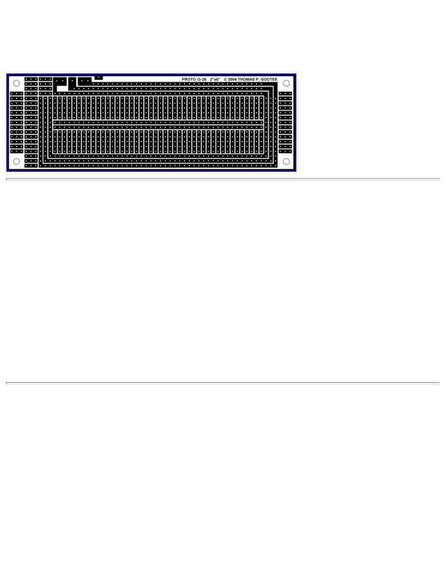
FREE PROTOTYPE BOARD PATTERN DOWNLOAD:
http://www.fullnet.com/u/tomg/gooteepc.htm (7 of 26)8/21/2006 11:09:55 PM
Easy PCB (Printed Circuit Board) Fabrication, Using Laser Printer Toner Trans...B, Wire Wrap, resist, photoresist, boards, fabrication , fabricator, LaserJet
(10/2005): Here's a bitmap pattern for a 2"x6" prototype board that I designed. You can download it for free (for your
personal use, only). Note that it's about a 540kB download.
RIGHT-click on the JPG image, below, and select "SAVE TARGET AS":
- Print the pattern, using the darkest laser printer settings (On my LaserJet 4, I use: Dithering: NONE, Intensity:
DARKEST, "Raster Graphics", "Print Truetype as Graphics", and RET (Resolution Enhancement Technology): OFF). If you
have a "Manual Feed" tray, such that the paper doesn't have to bend as many times, or as much, USE IT. [But I still
sometimes have to "help" the paper to keep moving, as it exits the printer. (Maybe my rollers are dusty?)]
- Never touch the board-part of the pattern paper with fingers, or with anything else, before OR after it's been printed.
- UPDATE (02/20/04): It has been reported that running the pattern through the laser printer (or copier) a SECOND TIME
(but without printing anything over the pattern portion), so the fuser can reheat it, makes the later process of removing the
paper MUCH easier. But you would need to print SOMETHING, or else the printer might not heat the fuser. I use an almost
blank image, with a tiny dot in one of the corners, that won't print where the pattern is. [NOTE: I don't do this step, any
more, since I started using the Staples paper.]
- Cut the pattern out (I use scissors), leaving at least 1/8-inch to 1/4-inch of extra paper, all the way around the pattern, and
an inch or more on ONE of the shorter sides (to grab it by). Lay the pattern flat, face-up, until it's ready to be used. [Update
(10/2005): I now often cut as close as possible to the pattern, on three sides.]
UPDATE: LINING UP THE PATTERNS FOR 2-SIDED BOARDS:
(10/2005): I've been making lots of 2-sided boards, lately, and have found a very easy way to routinely get very good
alignment: First, I always include the board outline, on the drawings of the patterns. After printing the patterns for the two
sides (Note that the pattern for the TOP copper needs to be REVERSED.), I use scissors and cut right on the board-edge line,
on TWO (adjoining) sides of each pattern, making sure that the two sides and corner that I end up with are for the SAME
corner, on both the top and bottom patterns. I then get a "coarse" alignment by laying the two patterns together, with the
printed sides facing each other, and standing them up together, on a flat surface, on the two cut sides. Then I hold them up to
a bright light and try to get the best-possible alignment. (Note that if your top and bottom patterns don't have enough
common items that can be used to align them, you can print special alignment marks, probably in at least two diagonally-
opposite corners.) Then I somehow manage to tape the patterns together. But I DON'T tape them on the two cut sides. When
I'm ready to do the transfer, I slip the prepared blank board in between the pattern sheets. I use the two cut sides and the
corner to align the pattern with those two board edges, giving excellent alignment between the two sides. (Note that the two
UNCUT sides, which are taped in one or more places, should probably be as large as possible, so that their edges are
http://www.fullnet.com/u/tomg/gooteepc.htm (8 of 26)8/21/2006 11:09:55 PM
Easy PCB (Printed Circuit Board) Fabrication, Using Laser Printer Toner Trans...B, Wire Wrap, resist, photoresist, boards, fabrication , fabricator, LaserJet
relatively far away from the edges of the board, to prevent any possible small errors due to unequal bending of the paper
around the PCB's edges.)
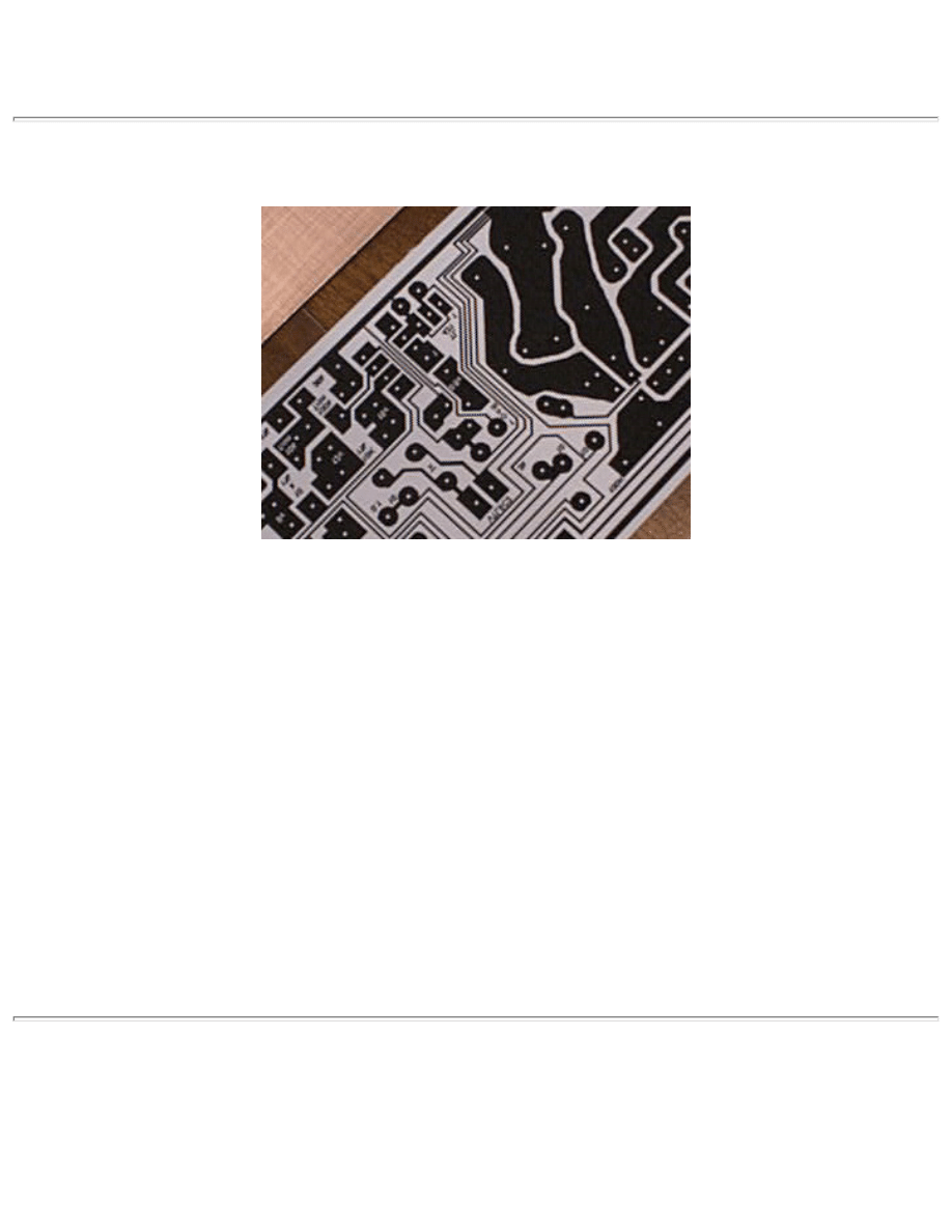
A portion of one of my laser-printed PCB patterns:
Size references, for the photo:
The smallest trace-thickness that is shown is 4/300ths of an inch (about 0.0133 inch, or 0.000523 cm). And, at the top of the
photo, some of the traces are separated by only 2/300ths of an inch. (It doesn't show up very well in this photo. But it works
well in actuality.)
Also: the printed portion of the board pattern is about 2.25 inches across, the shortest way.
And: the drill-holes' location-markers, on the solder pads, were made by drawing squares, with sides with lengths of 6/300 of
an inch (i.e. 1/50th of an inch).
There is also an 8-Pin DIP IC location, slightly above and to the left of the center of the photo, where the distance between
adjacent holes' centers is exactly 0.10 inch.
Note that I do not yet know what the smallest practical acheivable trace-width is, for this PCB method. (But, although it's not
pictured here, I have recently made boards with some traces that were about 2/300ths of an inch wide, which ran between the
solder pads of two adjacent IC pins, with absolutely no problems. Those boards turned out perfectly fine, using the toner-
transfer method described here.)
- Scrub the board with a Scotchbrite or "artificial steel wool" pad (nylon abrasive pad), equivalent to '0' steel wool, usually
in two orthogonal directions (with a lighter pass or '000' equivalent at the end, so it's not TOO rough). (I do *NOT* use
REAL *steel* wool, since it WOULD cause RUST/oxidation, after it's embedded in the copper.)
[Note that if you have to cut the blank pcb out of a larger piece, you will probably have to use a metal file, to make sure that
http://www.fullnet.com/u/tomg/gooteepc.htm (9 of 26)8/21/2006 11:09:55 PM
Easy PCB (Printed Circuit Board) Fabrication, Using Laser Printer Toner Trans...B, Wire Wrap, resist, photoresist, boards, fabrication , fabricator, LaserJet
the edges are smooth and that they don't protrude above the rest of the copper surface, at all. A small, fine-grooved "mill
bastard" file works well. [I have been told that commercially, a SHEAR is usually used to cut pcb material. I currently use a
small bandsaw, with a fine-toothed blade, with a very small opening so the blade can't twist very much (a wider blade helps
with that, too). I used to use a small hand-held reciprocating-type jigsaw, with a metal-cutting blade installed. And, before
that, I used a hand-held metal-cutting hacksaw.]
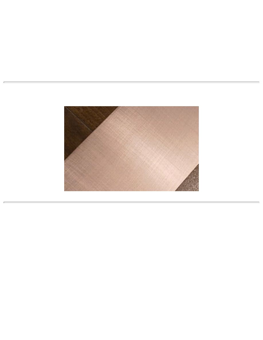
The "scotchbrite" step does TWO things: 1) It removes oxidation, stains, scratches, etc, so the copper surface of the PCB is
all uniformly nice and shiny. (You might have to press very hard, for this part.) And, 2) It makes the copper surface
somewhat LESS than perfectly smooth. The nylon abrasive pad makes many tiny scratches in the copper. This apparently
helps the toner to stick to the copper. (Press very lightly, near the end of this part.)
PCB Surface after rubbing with abrasive pad:
- Scrub the board with a paper towel soaked with ACETONE solvent. Keep doing it until (almost) no more discoloration
is seen on the paper towel. Press hard! And keep switching to clean parts of the towel.
- Lay the board (with the copper side facing up) on a rigid, flat, heat-resistant surface, such as a smooth piece of wood or
plywood. Blow any dust, etc, off of it, if necessary, very carefully, and off of the pattern paper. Lay the paper pattern face
down on the copper, lining it up exactly right.
- I use a regular handheld household electric CLOTHES IRON, set as HOT as it will go, i.e. the MAXIMUM temperature
setting (called "Linen", on mine, just above the "Cotton" setting), with no steam. (I have not measured the actual temperature
of the iron. I will try to do so, at a later date, and update this page.)
- Place the iron on the back of the pattern. Pre-heat the whole board. i.e. Hold the iron on the whole pattern, if possible
(unless the pattern is too large), for at least 1/2 minute or more, pressing firmly (see addendum, below, for pounds of force
used). I usually am standing next to a 30-inch-high table that the pcboard is on, and just "lean on" the iron, somewhat, during
this step.
I usually MOVE the iron a little bit, after about half of the time has passed, just in case the holes on the bottom of the iron, or
some other factor, might cause a non-uniformity problem.
http://www.fullnet.com/u/tomg/gooteepc.htm (10 of 26)8/21/2006 11:09:55 PM

Easy PCB (Printed Circuit Board) Fabrication, Using Laser Printer Toner Trans...B, Wire Wrap, resist, photoresist, boards, fabrication , fabricator, LaserJet
Note that almost as soon as the iron first touches the pattern and presses it against the board, the pattern will no longer slip
on the copper. So, sometimes I put the iron on a small portion of the pattern (a corner, or the smaller end of a board, usually),
at first, for five or ten seconds, while I hold the pattern in position with my other hand. This prevents the pattern from
slipping, just as the iron is applied, especially if the pattern paper is slightly curled, or the iron is applied too slowly, or with
some lateral motion, etc etc.
UPDATE for 2-Sided Boards:
(10/2005): I usually preheat BOTH sides of the board, first, before starting the ironing.
- After the board is well-heated (after the 1/2 minute or more, in the previous step), I place the rear of the iron along an edge
of the board (with the rest of the iron on the board), and press hard near the rear of the iron's handle. I move the iron 1/4 to
1/2 inch away from the edge and press hard again, for about a half-second to a second, and continue that way until I'm near
the other side of the board (with the rear of the iron), and it gets hard to keep the iron flat against the board. Than I go back
the other way (starting from the opposite edge), doing the same thing, over the same part of the board. If there are board-
edges that are wider than the iron's rear edge, I make overlapping passes, with the iron's side being along the outer edge of
the board, on both sides of the wide edge. I usually do this whole procedure starting from each of the four edges of the board.
- Sometimes, at this point (and periodically, whenever it seems like it might be necessary), I reheat the whole board for ten
seconds or so, or more, with moderate to heavy pressure on the iron, just like at the beginning.
Update (10/2005): The FOLLOWING step is important. As of 10/2005, it's usually about all I do, as far as the actual ironing
part. And (I usually now DO raise the rear of the iron, very slightly, in order to get more pressure at the tip.)
- I then always go over the whole board with the TIP of the iron, keeping it FLAT but torquing the iron "forward", as I go,
moving either side to side on the board or pulling the iron backwards, in lines about a quarter-inch or less apart, across the
whole board. But I'm careful to never let the tip "gouge" or "dig in", and never let any EDGE of the iron press against the
board by itself. i.e. I always try to keep the bottom of the iron FLAT against the board, no matter what else I'm doing.
- If you see the pattern starting to show, through the paper, then you have probably done it well-enough. (Or is that just some
kind of black stuff from the bottom of my iron rubbing off onto the areas over the slightly-raised pattern?)
- At the end, I usually reheat the board (with pressure on the iron at the same time, again). I also usually just press the iron
flat against the board, hanging almost halfway off one side, then in the middle, then off the other side (still always keeping it
flat against the board), for good measure...
- The entire heating/ironing process usually only takes between two and three minutes.
- Then, usually within five or ten seconds or so, I pick up the board (i.e grab it by the edge of the pattern paper) and drop it
into hot water. [A minute or two of delay doesn't seem to matter, at this point.]
I usually use a small rectangular glass baking dish (or a sink), full of hot water (about 130 deg F or more; mine is usually
about 140 degF), letting the board soak for 10 or more minutes. [Update (10/2005): I usually try to carefully peel off as
many layers of paper as I can, within about two minutes, and then re-wet or re-soak the board when I get down to dry layers,
or the last layer.]
http://www.fullnet.com/u/tomg/gooteepc.htm (11 of 26)8/21/2006 11:09:55 PM
Easy PCB (Printed Circuit Board) Fabrication, Using Laser Printer Toner Trans...B, Wire Wrap, resist, photoresist, boards, fabrication , fabricator, LaserJet
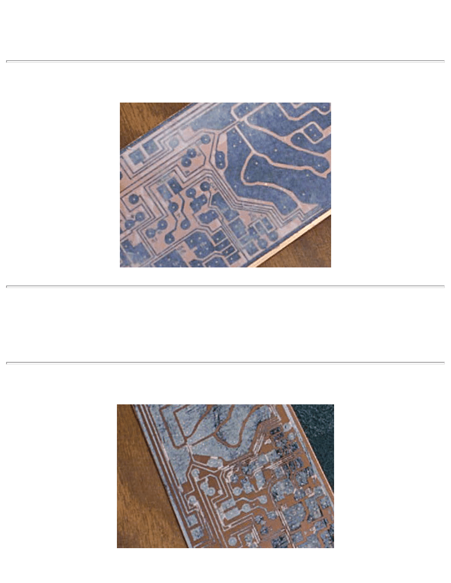
- Peel off the paper, or at least the TOP layer or two. If the paper underneath is still a little dry-ish, put the board back into
the water, for another ten minutes or more.
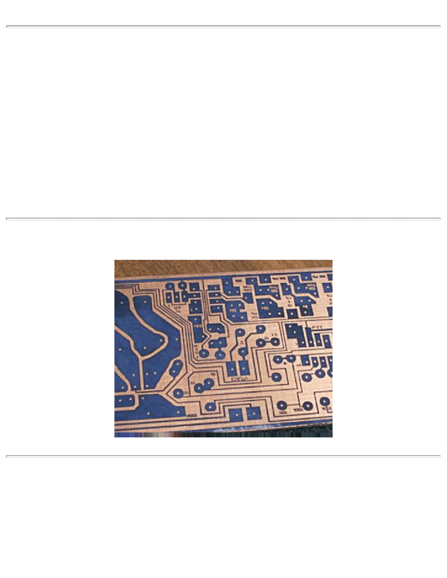
PCB after soaking, with all but one layer of paper peeled off:
- Rub the remaining paper off, with thumb pressure (or a toothbrush or other soft brush). It's OK to rub fairly hard. But
your thumbs' skin may get sore. Usually, almost all of the paper residue comes off, even off of the toner itself. So, you could
SEE if there were any pinholes, etc, in the toner. (I have yet to see any defects, though, using the Staples Picture Paper.)
Note that it doesn't matter if there is paper residue that remains on top of the TONER.
PCB after final soak, with most of the paper rubbed off:
http://www.fullnet.com/u/tomg/gooteepc.htm (12 of 26)8/21/2006 11:09:55 PM
Easy PCB (Printed Circuit Board) Fabrication, Using Laser Printer Toner Trans...B, Wire Wrap, resist, photoresist, boards, fabrication , fabricator, LaserJet
At this point, if something has gone wrong, you can start over and not waste the board, by washing the board with laquer
thinner (see below), to remove the toner. Then, begin again with the second (Scotchbrite) step, above.
- Use small circular motions with a toothbrush, or some other small, relatively soft brush (but not with metal bristles!), to
remove paper residue from small or tight areas, and, especially, from the drill-hole "marks", and any small text. This used to
be the hardest, or most tedious, part. But with the Staples "Picture Paper", this step isn't too bad, at all. And you can usually
rub pretty hard, with the brush, without damaging the toner at all (unless you didn't iron it correctly). Small circles with the
brush, keeping the bristles mostly un-bent, and using their tips to dig into areas that need it, seems to work well.
Update (10/2005): I have found something that's quite a bit better than a toothbrush, for removing the last bits of paper,
from, for example, drill hole marks and gaps between very close traces: I now use a wad of wet "Crinolin" material. It's a
type of fabric, which, I believe, was used to make women's petticoats, in the past. It's a coarse material, i.e. with threads far
apart, and is somewhat "springy". Mine was acquired in the form of handmade kitchen scouring pads. But anyone at a fabric
store (probably even Walmart's fabric/sewing/hobby department) ought to know what Crinolin is, and be able to provide
some, or something very similar.
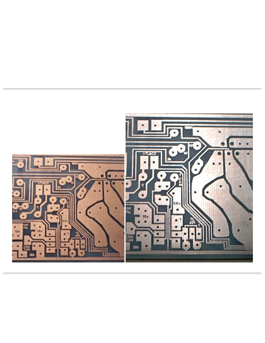
PCB after removing enough paper; ready for etching:
- Rinse the board and wipe the board dry with a clean paper towel. [Update: Now I usually wash it with soap and warm
water, and then rise and dry it, just to make sure that all of the paper's residues have been removed, pretty well.]
- Make any necessary corrections, using a Sharpie or other etch-resistant marker pen. I sometimes have a couple of very
small flakes of toner fall off, on about one out of three or four boards, at the most, especially if I scrub way too hard with the
toothbrush. [But almost NEVER, any more, now that I use the Staples paper! I did manage to slightly-damage the toner on
*one* board, because I wanted to see if I could use a very stiff, large, kitchen-type scrub-brush. I rubbed extremely hard.
http://www.fullnet.com/u/tomg/gooteepc.htm (13 of 26)8/21/2006 11:09:55 PM
Easy PCB (Printed Circuit Board) Fabrication, Using Laser Printer Toner Trans...B, Wire Wrap, resist, photoresist, boards, fabrication , fabricator, LaserJet
The board was clean in seconds. But I pressed a little too hard and took small parts of just the edges off of a few traces and
pads.]
- Etch. [UPDATE (10/2005): ALSO SEE NEW ETCHANT UPDATE, FARTHER ABOVE!] I use Ferric Chloride, in a
tupperware-style plastic food container, in a sink of hot water. I used to agitate it by rocking the container. Now, I use latex
gloves and hold a pcb in my hand and either sweep it back and forth in the etchant, or, hold it flat and push it up and down
vertically. I also usually keep an eye on the progress of the copper removal and sometimes rub on the areas where the
removal seems slower, with my thumb or fingers. I have also been told by one person that they just used a balled-up paper
towel with some etchant on it, and rubbed the board until all of the copper was gone, with very good results, although I've
never tried that method, myself. I did recently get a great deal on a very nice "automatic" etching tank, at an auction. But it
says that only the persulphate etchants should be used in it. So I haven't gotten around to trying it, yet.
PCB after etching and drilling:
- Don't get the etchant on ANYTHING else, especially a good stainless-steel sink(!) (or your clothing). I keep the lid loosely
on the container, to catch any splashes. Don't use a metal container! And don't use any metal utensils, if you want to use
them for anything else, ever again! Wipe and flush any accidental spills with lots of water, IMMEDIATELY. The ferric
chloride will also stain your skin. Wash it off immediately, if possible. One time, when I was using a latex glove, and
moving a pcb around in the etchant with my hand, I later discoverd that there was a hole in the glove, and that the glove had
been filled with etchant for about 15 minutes. I had one hand that was brownish-yellow, for several days, heheh.
http://www.fullnet.com/u/tomg/gooteepc.htm (14 of 26)8/21/2006 11:09:55 PM

Easy PCB (Printed Circuit Board) Fabrication, Using Laser Printer Toner Trans...B, Wire Wrap, resist, photoresist, boards, fabrication , fabricator, LaserJet
Note that many people prefer Ammonium (or another) Persulfate (or persulphate? sp?) as the etchant. One big advantage is
that it is more or less transparent, allowing you to see the progress of the etching, without removing the board from the
etchant. Note also that most people either agitate the etchant by hand, or use an air-bubbler tank. With an air-bubbler tank,
etching times can be as low as 5 minutes, and etching is more-uniform. A bubbler-tank, with a heater, can easily be built,
using plexiglas (or a Tupperware breakfast-cereal container?), silicone sealer (caulk-type stuff), a fish-aquarium pump and
tubing, and an aquarium-type water heater. I believe there are contruction plans on the Web. If anyone has a link, please let
me know, so I can post it, here. [I think that commercial/industrial PCB-etching systems use a fairly forceful SPRAY of
heated etchant, onto vertically-oriented boards. But you'd need a special (probably magnetically-coupled) pump, with no
internal metal parts exposed to the etchant being pumped.]
(See farther below, for some links to etching tanks, etc.)
Note that if you use "1-ounce" copper boards, instead of "2-ounce", etching is much faster, and, correction-pen marks might
actually last long-enough to work fairly well. Plus, over-etching isn't usually as much of a problem.
- When etching is almost complete, I used to remove the board, rinse it under running tap water, and put it in a small tub of
half-strength etchant (diluted 1:1 with tap water), and lightly brush the areas that still had visible copper, until they had been
removed. This seems to help prevent over-etching. [Update: Now I usually just wear latex gloves and rub the board with my
fingers, in the full-strength etchant tub, to remove any "stubborn" areas.]
- Wash the board in "Lacquer Thinner" solvent [See the UPDATE, in the next paragraph.], rubbing with a paper towel, to
remove the toner INSTANTLY. But be careful: Laquer thinner is *extremely* volatile/flammable/explosive! (And it's bad
to get on your skin.) I do it outside. I use small, disposable thin aluminum pans, which are usually used for temporary food-
storage (pie pans, for example). (Mine are usually free, and filled with hot-and-spicy Szechuan or Hunan Chinese food,
initially.) I generally lay the board face-up in the pan, and then pour laquer thinner over it, to a depth of about about 1/8 to
1/4 inch (1/2 cm), or less (as little as possible; A thinner-soaked paper towel or two works, too.). Then I wad a paper towel
into a ball, and lightly rub the toner off. I then pick up the board and wipe off any remaining traces of toner. I suppose that I
really wouldn't need to pour as much thinner into the pan. Possibly, it would even work as well with just a thinner-soaked
paper towel. [Also, make sure to clean your hands, with the thinner, if any dissolved toner get on them. It's very difficult to
remove, otherwise. However, the thinner is said to tend to cause cancer. But I haven't yet really tried to find a good way to
do it without getting some on my hands.]
Update (10/2005): I now use Acetone, instead of Lacquer Thinner, to remove the toner. And I don't use a tub of it. I just
soak a folded-up paper towel with Acetone and wipe the toner off of the board. (Note that Acetone is also bad to get on your
skin.)
- Drill the holes (if your PCB is for through-hole components, as opposed to the newer surface-mount). Some people have
suggested drilling BEFORE you etch. OK. But I like the way the etched hole marks help guide my drill bit into themselves,
especially on small pads and when holes are very close together, or when the drill/bit is a little wobbly.
I used to use a regular floor-standing drill press, set at its highest RPM (revolutions per minute). I had tried the solid-carbide
PCB bits, about .035 inches, with the larger, 1/8-inch shanks. But they are so strong that they're too brittle, and they broke
too often, for me. (Even getting 50 of them for $5 at a hamfest didn't seem like a good deal. That's how often I broke them!)
So, I usually just got the "wire-gauge" high-speed steel drill bits, from the local hardware store. I'd been using the #60 (.04
inch), since they fit a large variety of component lead sizes (all but the largest). I got 15 bits for about $20. I changed bits
every few hundred holes, at the most, or whenever I noticed the edges of the holes were getting pulled away from the board
too much. I guess the FR-4 board material doesn't transmit heat well at all, and the steel bits get hot quickly, and
consequently dull very quickly. (It has been suggested that putting Carbosol on the bit occasionally may prevent it from
dulling as quickly. I tried it, but didn't notice much difference.) To hold the tiny bits in my large drill, I had to also buy a
small chuck that fits into my larger chuck.
http://www.fullnet.com/u/tomg/gooteepc.htm (15 of 26)8/21/2006 11:09:55 PM
Easy PCB (Printed Circuit Board) Fabrication, Using Laser Printer Toner Trans...B, Wire Wrap, resist, photoresist, boards, fabrication , fabricator, LaserJet
UPDATE: I (my son, actually) modified a small, cheap drill press to have very precise linear motion, and removed its old
drill head and made a precisely-positioned mounting that holds a dremel-like rotary tool that runs at about 30,000 RPM. So
now I CAN use the 0.032 and 0.035-inch solid-carbide PCB drill-bits. And they are GREAT! I've never seen one even
START to get dull, because I always end up breaking them after a few thousand holes, at the most (by accidentally hitting
them with my finger or hand, usually).
If you're interested in modifying a small drill press, to make it more precise, here's what my son did to mine: First, he
removed the old, cheap drill motor assembly and used some large U-bolts to mount my Dremel clone to the part of the
drillpress that moves up and down (he may have had to weld a mounting plate on there, first, too). Then, he used a section of
a bendable metal strap with holes in it (forget what it's called, exactly) and made a "U" shape out of it, and attached that to
the moving part of the mechanism, above and/or behind where the dremel was mounted. Then he attached two strong
springs, between that metal strapping and the NON-moving part of the mechanism. The springs are the key. They are strong-
enough that they don't allow any horizontal "play" in the mechanism. But they're long-enough (a few inches, at least) that
when the drill is moved up and down, they don't impede the vertical motion. (Of course, I only use about a half-inch of
vertical motion.)
Many people have had good success using a Dremel tool, with the Dremel drill-press/stand adapter. At least one person
reported also using a large magnifier, at the same time. This would also help give eye-protection. Otherwise, safety glasses
(eye protection) should be worn.
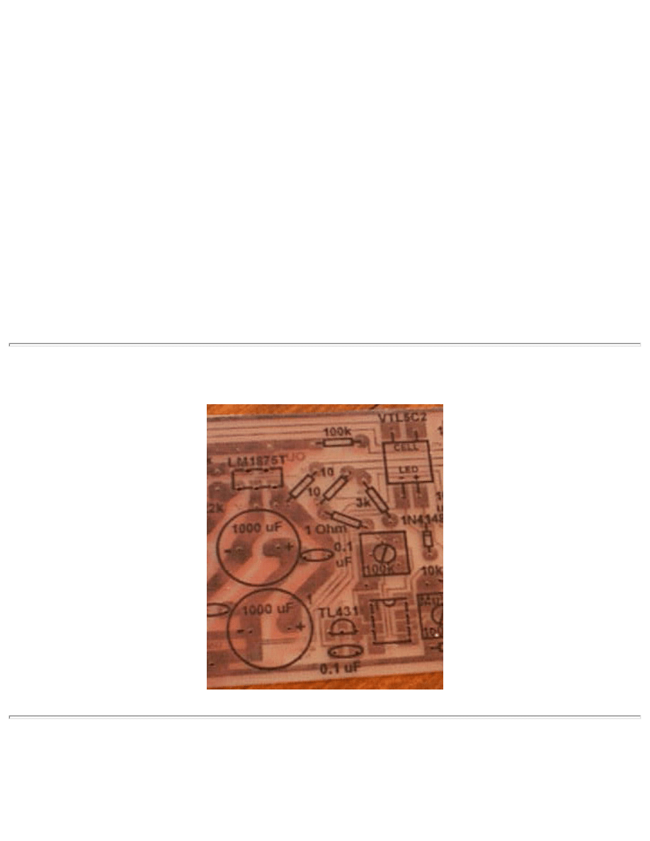
PCB component-side with artwork applied:
- If you're going to put artwork on the COMPONENT side of the board [Recommended(!), especially since it's SO EASY
to do; much easier than doing the copper side.], scrub it with the Scothbrite pad, at this point, with the same method that was
used for the copper side. Then do an "acetone rub", with a paper towel, until no more "dirt" comes off, as was done for the
copper side. Make sure the holes are all dried out. (Tapping each edge of the board sharply on a hard surface can help to
http://www.fullnet.com/u/tomg/gooteepc.htm (16 of 26)8/21/2006 11:09:55 PM

Easy PCB (Printed Circuit Board) Fabrication, Using Laser Printer Toner Trans...B, Wire Wrap, resist, photoresist, boards, fabrication , fabricator, LaserJet
dislodge any liquid that's still in the holes. Then re-dry and allow to air dry for a minute.)
Note that the pattern has to be the drawn as the REVERSE IMAGE of what it will look like after it's applied to the board.
- Hold the board and the pattern sheet together (usually printed on the other, more-easily-removed, "JetPrint Multi-Project"
paper, mentioned above) in front of a very bright light, to align the component markings with the holes' pattern. (If your
boards aren't translucent, this method may be a problem.) Then iron the component-side pattern onto the fiberglass side of
the board, using the same technique as was used for the copper side.
- Soak for five or ten minutes in warm water and then just peel off the paper. Rinse and lightly rub the very minimal residue
away, dry the board (and maybe wash with liquid soap and warm water), and it's ready!
The boards made this way come out nearly perfect, nearly every time.
UPDATE: HOMEBREW PCBS DISCUSSION GROUP:
I highly recommend the Homebrew_PCBs discussion group, at http://www.yahoogroups.com.
There are also some other very good discussion groups, there. I like the LT-Spice group, and also the Electronics_101 group.
UPDATE: FREE LT-SPICE SIMULATION SOFTWARE:
If you don't yet have the free LT-SPICE schematic/simulation software, you should definitely GET IT!! I use this
software A LOT. (It's also known as "Switcher CAD III", or something like that. But it's a truly-general-purpose full-
featured Spice simulator, with an excellent user interface, and with VERY EASY schematic drawing, etc. And it's totally
FREE, from Linear Technology Corporation's website:
Just look for "Free SwitcherCAD Download", in the left-hand column of the linear.com webpage, above.
ADDENDUM:
Well, I tried leaving the paper residue IN the holes and etching. But the result was less than satisfactory. So, in order to
minimize the potential for damage to the traces from hard rubbing with the brush, I tried letting a board soak overnight in
water. Voila! The drill holes were easily cleaned out with fairly light scrubbing with the toothbrush. Of course, I usually
can't wait overnight. Adding some liquid dish detergent helps, if I'm in a hurry. Also, digging the bristles on the tip of the
brush straight into the holes, while lightly making tight circular motions, gets the residue out with minimal brush pressure. It
is still quite tedious, if there are lots of holes. Any suggestions?
Also, I DID put a bathroom scale under the iron, and simulated pressing on a board. I was using at least 25-30 LBS (pounds)
http://www.fullnet.com/u/tomg/gooteepc.htm (17 of 26)8/21/2006 11:09:55 PM

Easy PCB (Printed Circuit Board) Fabrication, Using Laser Printer Toner Trans...B, Wire Wrap, resist, photoresist, boards, fabrication , fabricator, LaserJet
of force. I don't always use the same PSI (pounds per square inch), apparently, because I use the same force on board sizes of
4x6 inches and 2.375x6 inches. Both seem to come out equally well. I have, several times, used a lot more force on the iron,
and it IS possible to flatten out or blur pads or traces, if I press hard enough, or if I accidentally scrape with the edge or tip of
the iron instead of keeping it flat.
Someone else suggested baking the boards in an oven, after the toner has been applied and before etching. With my current
paper and method, I don't see why it would be necessary, since the toner seems so strongly bonded to the board. However,
back when I was using paper that left pinholes in the toner, I wanted to try baking a board just to see if the pinholes would
close up. At the time, it also seemed like heavier iron pressure might close them. But it never seemed to. Now that I'm using
the Staples Picture Paper, I don't need to worry about those things, any more.
However, I WOULD like to try to find a more "automated" way of applying the toner pattern to the copper, instead of
ironing. i.e. It would be good if I could do many boards at once. And it would be good if I didn't have to stand there, the
whole time. I may experiment with using an oven, perhaps putting the boards under some heavy, flat piece of metal, or
clamping them between two pieces of metal, or something similar. I suppose that a similar thing could be done with a large
electric skillet, or something on a stovetop. BUT: I don't know how important the *motion* of the iron is, to the success of
the procedure. Perhaps it only helps by providing sufficient pressure. So, first, I'll probably try a sort of simulation, using the
clothes iron but without moving it laterally at all, and maybe experimenting with different amounts of weight on the iron. If
anyone has done anything similar, please let me know.
Happy board-making, everyone!
EMAILS that I've received and sent:
Hello,
I just wanted to say thank-you for posting (and with such detail) your new method for making PCB's. I've made printed
circuit boards for over ten years using the toner transfer method with expensive ($1.00 per sheet) TEC-100 transparency film
and it has never worked well. Some of the toner would peel off the copper blank, and I would have to draw in the missing
parts with a resist pen. In any case, I was always disappointed with the final result because it looked so poor, and it was
always such an ordeal, that I never wanted to make another PCB again.
All I can say is THANK-YOU!!! I've made 3 boards with your method, and every one has turned out perfect. The traces are
so clean and I'm amazed how well the toner holds to the copper. I was leary at first about peeling off the paper without
taking the toner with it, but now I don't worry at all. In fact the toner holds so darn well, that I have a tough time using an
abrasive to get it off after etching. Guess I'll have to get a chemical stripper.
So once again, thank-you for not only discovering this method, but more importantly for freely sharing it with everyone, and
with such well written documentation.
Thomas F
Bob,
http://www.fullnet.com/u/tomg/gooteepc.htm (18 of 26)8/21/2006 11:09:55 PM

Easy PCB (Printed Circuit Board) Fabrication, Using Laser Printer Toner Trans...B, Wire Wrap, resist, photoresist, boards, fabrication , fabricator, LaserJet
Thanks for inquiring! And thanks for the kind words.
The blank printed circuit board material can be purchased from
, which is the cheapest place I've
found, on-line, so far, for *NEW* PCB board material.
They have 12x12-inch single-sided 1-oz-Cu/sqft boards (Mouser part number 501-FR12x12S), for $8.36 for qty (1), with
lower pricing for larger quantities.
And they have a 4x6-inch version of the same thing, Mouser part number 501-FR4X6S, for $1.96 for qty (1).
Mouser.com also has double-sided PCB blanks, which are available in the same sizes as the single-sided ones mentioned
above.
, they have 1-sided 3x5-inch PCB blanks for $1.89 each (bgmicro's part-number ACS1380).
You should definitely get Mouser's catalog mailed to you, too. They are usually the cheapest supplier I can find, and have a
very wide selection of electronic components, parts, supplies, tools, hardware, equipment, etc etc. Their latest catalog has
1298 pages. And they're easy to order from, on line.
I also like
, for certain things. WHEN they have something, it's usually even cheaper than mouser.
com. And their service is at least as good, and may be even better.
For cutting the PCBs to size, a bandsaw would be great, I think (although, commercially, I believe that they use a SHEAR).
You might need the appropriate fine-tooth blade, maybe even one for cutting soft metals (although the thin copper hardly
counts as "metal", as far as cutting-tools are concerned). The FR4 fiberglass board material may actually be more of a
problem. It doesn't transmit heat well, at all, which results in very fast heating of, for example, stainless steel drill bits, if
they're used on it, which dulls them EXTREMELY quickly. The same MAY be true for saw blades, although I have been
using a small jigsaw-type saw (relatively low speed), with actual metal-cutting blades (very similar to a metal-cutting
hacksaw blade, which I have also used, when I did them without a power saw), WITHOUT noticeably-fast dulling. Of
course, it doesn't do a very good job, since it's handheld. I have been planning to buy one of the small bandsaws, available
for around $200 new. A table saw, or a "cutoff saw", or a "radial arm saw", seem like they might work well, too, with a thin,
fine-toothed blade.
For drilling, though, since I have started to make larger quanities of PCBs, I have changed from using SS bits to using solid-
carbide PCB drill-bits, which I run in a small drillpress that holds a Dremel-like rotary tool, running at about 30,000 RPM
(which should be the MINIMUM, for the solid-carbide bits, I've been told, since they are said to run best at 100,000 to
200,000 RPM). With the #60 wire-gauge (0.04 inch) hardware-store SS bits, I was getting about 150 to 250 holes (and
maybe way fewer) per bit, before it was so dull it was actually starting to pull the copper up off the board a little, around
each hole. (And I did try using various lubricants, to no avail. Maybe a water-jet would help...) With the solid-carbide bits,
which are also nicer because they have a 1/8-inch shank, I've drilled several thousand holes in a row without ANY noticeable
dulling. I usually break the bits, sooner than that (they can break very easily with just a little side-pressure from one finger).
So I've never even seen one START to get dull.
Needless to say, if you have any run-out (wobble) in your drill, the carbide bits will break almost instantly. My large, cheap
drillpress could never begin to use them. I had to modify a small, cheap drillpress that I found laying around, to make it very
precise in its linear motion, and also to remove its old drill head from it and precisely and rigidly mount the small rotary tool
on it. But I think there are commercially-available small, precision drillpresses, suitable for the small high-speed rotary tools,
for less than $100 (maybe from Dremel?).
http://www.fullnet.com/u/tomg/gooteepc.htm (19 of 26)8/21/2006 11:09:55 PM

Easy PCB (Printed Circuit Board) Fabrication, Using Laser Printer Toner Trans...B, Wire Wrap, resist, photoresist, boards, fabrication , fabricator, LaserJet
Note, also, that you can usually find boxes of 50 or so of the solid-carbide PCB drill bits, probably used, re-pointed ones,
which seem to work just fine (that's what I've been using), for about $5-$10, either at larger hamfests (see www.arrl.org for
schedules and locations) and on www.ebay.com (but maybe for more, up to around $20 a box, on ebay). And there are some
places online that sell them, too. I like the 0.032 and 0.035-inch sizes, currently, for my through-hole stuff (but maybe
because those are some sizes that I happen to have on hand). The sizes around 0.04-inch work "OK", but are really a little
too large.
Sorry to blather-on for so long about all of that!
I get the Ferric Chloride etchant from www.jameco.com, their part number 70201 is in powdered form and makes one pint of
etchant, when mixed with water. One pint seems to etch at least a couple square feet of the 1-oz board. (The 2-oz/sqft copper
PCBoard would take twice as long to etch and use twice as much etchant.) Heating the etchant speeds the etching process, as
does agitating the etchant or the board, while etching.
When I do one board at a time, I sometimes use a plastic tub of etchant, which sits in hot water in a sink. I wear rubber
gloves and hold the board with my hand, continuously swishing it around in the etchant (no splashing, hopefully). I also
usually rub my (gloved) fingers on the parts of the board that are etching more slowly, which speeds the copper's removal a
little, in those areas. Every once in a while, I remove the board, rinse it, and hold it up to a bright light (and also reflect light
off of it), to better-see what's left to remove. Etching for TOO LONG a time (any longer than absolutley necessary) can tend
to degrade the quality of the finished board's tracks, especially their edges.
When etching takes much longer than it usually takes, the etchant is getting too weak (spent; used up). I have HEARD
rumors to the effect that one can add a common chemical to the Ferric Chloride, to rejuvenate it (Hydrochloric acid, maybe?
Can't quite remember. [If so, it's available from any hardware store, very cheaply, as Muriatic Acid. But **BE CAREFUL**
with it!] Check the Usenet newsgroups archive for the correct info [See below].).
Be careful with the Ferric Chloride, too. It won't burn you, under normal circumstances, as far as i know (I've had rubber
gloves full of it for 30 minutes at a time, before, hehe ["hole in glove"]). But it STAINS almost everything. And it seems to
permanently disfigure almost any type of metal that it touches, even for a moment. (So don't use it in your good stainless
steel sink!) It might hurt metal pipes, too, if it's very concentrated. In some areas, too, it's illegal to dump it down the drain,
even if diluted. There are safe and relatively easy de-activation and disposal methods, explained on the Usenet neswgroups
(see below). And, I've HEARD that Oxalic Acid can remove the colr from the stains. Oxalic acid is available in the form of
some common products.
I "KNOW" that there has to be some un-related industry (wastewater treatment, maybe; or agriculture?) that uses either
Ferric Chloride or one of the persulphate etchants IN BULK, which should lead to a MUCH cheaper source of supply. But I
haven't found them, yet. (That reminds me of when I made wine and beer, in the distant past. I eventually found that
IODOPHOR solution was by far the best thing to use, to sterilize bottles, fermenters, siphons, tubing, fittings, etc,
BECAUSE IT NEEDED NO FINAL RINSE. But the homebrew supply shops wanted $5 to $10 for about 5 ounces of the
concentrate. Then, one day, I was perusing the inventory of a local FARM-SUPPLY store, and found out that THEY sold it
BY THE GALLON, for $12 per gallon jug! Apparently it's used to sterilize dairy-farms' milking equipment. I've HEARD
that there are similar situations, pertaining to etchant chemicals, but am still looking.)
You can also make your OWN etchants (hydrochloric acid and hydrogen peroxide is one mixture, I think. But you'd have to
search the Usenet newsgroups to find the proper concentrations and ratios, etc (see below). OR, you could use one of the
persulphate etchants.
You can find a LOT more (and probably better) information, about ALL of this stuff (and much more), by searching the
Usenet newsgrouops archive, at http://groups.google.com. It's truly a goldmine!
http://www.fullnet.com/u/tomg/gooteepc.htm (20 of 26)8/21/2006 11:09:55 PM

Easy PCB (Printed Circuit Board) Fabrication, Using Laser Printer Toner Trans...B, Wire Wrap, resist, photoresist, boards, fabrication , fabricator, LaserJet
Disclaimer: For all of the above, "try it at your own risk", and "your mileage may vary", and "not suitable for any purpose",
and "due to its graphic nature it should not be viewed by anyone", etc etc.
Good luck! Let me know if I can be of more help.
Regards,
Tom
Tom Gootee
tomg@fullnet.com
http://www.fullnet.com/u/tomg
----------
From: Robert
Sent: Tuesday, May 04, 2004 9:21 AM
To: 'tomg@fullnet.com'
Subject: Viola!
Dear Sir:
Thank-you for posting information on how to home-make PCB's. I was just at
the point where I needed to make some circuit boards without any prior
experience and only a vague notion of what had to be done--I never finished
a Heathkit I bought on how to do them.
Anyway, I couple of questions come to mind that you may be able to answer:
1) Vendors - who sells PCB's suitable for etching? My searches on the
internet have not been particularly successful and all I seem to dredge up
is a host of companies that want to make the boards for me. I certainly do
not get any entries for vendors.
2) Board sizes - in the marketplace, are there a variety of board sizes for
sale? I suspect, once I create the printer drawing that the board I will
need in quantity will measure no more than 2" X 4". Can either the one or
two ounce boards be cut easily? What would be used to size them, a band
saw?
3) Etchant - I will follow your lead and use ferric chloride. How many
boards can be etched per solution use? What is the indicator, if any, that
the etchant is no longer working--is the time it takes to finish a board
gets progressively longer? I have in mind approximately 20 identical boards
that need to be created.
Your time and attention to these questions is greatly appreciated. I look
forward to receiving your advice.
Sincerely,
Bob
http://www.fullnet.com/u/tomg/gooteepc.htm (21 of 26)8/21/2006 11:09:55 PM

Easy PCB (Printed Circuit Board) Fabrication, Using Laser Printer Toner Trans...B, Wire Wrap, resist, photoresist, boards, fabrication , fabricator, LaserJet
Hi Tom!
Thanks for your information on the toner transfer method for making PCBs (and congrats on your 15 minutes of fame!). I'm
really just getting into hobby electronics, and hope that as I learn more I will be able to put my projects on professional
looking PCBs using the technique you describe.
I work in a Staples store, and was excited to see a Staples product described as the perfect paper for this technique. However,
the barcode you give [Now corrected! -Tom] is not quite complete. A UPC bar code should have 12 digits -- leading and
trailing check-digits are critical! So the full code for Staples Picture Paper (30 sheets) is 7 18103 02238 5.
Unfortunately, even the complete UPC isn't cross-referenced on the Staples web site (doh!). Instead, use the SKU (item
number) for the paper: 471861. Just type this in to the search field on staples.com, or take the SKU to a store and ask a sales
associate to help you get the Staples photo paper with that SKU. (But don't just hand them the SKU and tell them to go get it
-- we're pretty good, but SKUs are more-or-less randomly assigned and we haven't memorized all 900,000 of 'em yet!).
If you want to save a little, or have LOTS of PCBs to make, the SKU for the 100-sheet pack is 471865, and the UPC is 7
18103 02241 5. [I already bought two more 100-packs, Woody! -Tom]
In case a store is out of the Staples brand (we work really hard not to be out of anything), here's the SKU and UPC for the
Canon paper you mention: SKU 501796, UPC 0 13803 01698 7. [But don't use it. -Tom]
I hope this helps you and your readers. I recently bought a LaserJet 1012 just so I could make PCBs, and when my skills
improve I really look forward to using it with your instructions so I can do something other than print PDFs.
Thank you very, very much again for your site!
Woody E.
Tifton, GA, USA
Crappy CYA Disclaimer: This email is not an official communication from Staples, and does not express Staples' policy or
position on anything. (This email may, however, state the official policy and position of the voices in my head.) Use the
information included within at your own risk. Blah, blah, blah, yadda, yadda, yadda.
Excellent website, by the way. Some suggestions to make pcb masks with toner a lot easier:
The main thing I do is to use transparency film instead of paper. HP Premium Transparency film (for Deskjet) works the best
so far, and prints very well in a laser printer. Place the film over the board, put a single sheet of paper over this, and iron in
the normal manner. You will find that you don't need to go to extraordinary lengths with the ironing, as you can actually see
the pattern sticking to the copper. Cool the board down, and carefully peel the film off. And that's all there is to it! No paper
to remove or anything.
Tip 2: Instead of steel wool to scour the copper, use 1200 wet-and-dry sandpaper under running water. It does not leave any
Fe in the scratches, and leaves a surface much better prepared. Rinse with boiling water, and dry immediately with a heat
gun. Place face down on a clean sheet of paper until ready for use.
http://www.fullnet.com/u/tomg/gooteepc.htm (22 of 26)8/21/2006 11:09:55 PM

Easy PCB (Printed Circuit Board) Fabrication, Using Laser Printer Toner Trans...B, Wire Wrap, resist, photoresist, boards, fabrication , fabricator, LaserJet
Doing it this way, I can make a PCB ready for etching in under 10 minutes!
P.S. Because it is intended for inkjet use, this film has some sort of matt coating on the print side. otherwise the ink beads up.
I don't know what it is made from, but it feels kind of 'starchy'. It is both a blessing and a minor 'problem'. I think the coating
is the reason that this type works better than plain transparency film. The matte coating seems to separate the toner from the
plastic base, and allow it to peel off easily. The minor downside is that some of this coating gets ironed onto the board as
well as the tracks, but it dissolves easily in the etchant that I use (Ferric Chloride), just takes a little longer than other board
areas. Shouldn't be a problem in your new bubble tank tho!
BTW, with the wet and dry paper, I usually have a bar of normal soap, and wipe the abrasive over it every now and then. It's
a standard technique used in metal polishing. It helps wash the grit and copper particles away, and has the added benefit of
degreasing the board at the same time. As you probably found out ages ago, grease is the enemy!
Hi Tom, I was reading the rest of your site and did a search on the paper you like. The manufacturer has a nice website with
a diagram explaining the multi-layer composition of their papers. They don't have a specific diagram for the photo graphic
heavy gloss, but it's probably like the four layer papers since the multi project paper is only three layers.
http://www.jetprintphoto.com/c/photopaper.asp
Just an FYI, -brice
Hi I recently found your web page well doing a search for an Octopus which is what I new it as when I was in the Navy
(Huntron Tracker) but I found it on the web as a (Analog Signature Analyzer) I found your site very interesting and I plan to
purchase a kit for your Curve Tracer II in May. I also found that the link on your PCB Etching page is invalid, Here are some
links to PCB Etching and the Homespun Page even has a home built plating tank, For people who want to try double sided
PCBs.
Here are the links:
http://www.thinktink.com/stack/volumes/voliii/homespun.htm
http://www.embeddedtronics.com/
http://aeinnovations.com:8080/projects/
I'd like to add a suggestion about how to dispose of used etching solution. Before you pour it in to the sink, pour it in a
plastic tank and drop there scrap of old steel nails, screws, small, nuts, bolts, etc., and let it stay for a few days. It will turn
the hazardous mix of copper chloride and Ferric Chloride (FeCl3) into copper powder (sludge) that settles on the bottom and
a non-etching and non-corrosive solution of FeCl2. It will save from corrosion, destruction and costly replacement in the
future your cast iron drain pipes and it will save from killing bacteria in the septic tank or in sewer treatment plant. They are
very sensitive to copper chloride and Ferric Chloride. A current law prohibits disposal of those chemicals in the sewer. For
best yet treatment, after separation of solution of FeCl2, mix it with solution of soda (Na2CO3 used as detergent) in a flat
http://www.fullnet.com/u/tomg/gooteepc.htm (23 of 26)8/21/2006 11:09:55 PM

Easy PCB (Printed Circuit Board) Fabrication, Using Laser Printer Toner Trans...B, Wire Wrap, resist, photoresist, boards, fabrication , fabricator, LaserJet
tray lined with plastic film. It will turn FeCl2 into Fe(CO3) (insoluble rusty mud) and NaCl (harmless cooking salt). After
drying outdoor whole dry rusty powder could be wrapped in plastic film and disposed of in the normal trash container.
I noticed your link to the Homemade PCB etching tank is dead. I remember seeing that before though and thinking it was
overly complicated. I made my own etching tank out of a $10 acrylic corner aquarium from PetsMart. It came with a small
pump and I just bought a clip on heater. I hot glued a thick straw to the bottom of the tank and poked a bunch of holes into it
and fed the air hose into the straw so there are lots of bubbles. I really have no electronics experience other than reading a
bunch of stuff and experimenting with breadboards, so I had to do this cheaply to justify it. It will easily hold up to a 7"x 7"
board which is more than I'll need. I think the total cost was around $25 so I was happy with it. I'm still trying to find a stick-
on high temp thermometer. Every time I find one, the place is sold out.
Tom, thanks for the comeback. I found just what I was looking for through google.
Bob
Centennial, Co
-----Original Message-----
From: Thomas P. Gootee [mailto:tomg@fullnet.com]
Subject: RE: Ammonium Persulfate
Bob,
Thanks for the email!
SInce I have only used ferric chloride, I can't answer your question.
But, you can do some searches at http://groups.google.com and find out.
Thanks again!
Regards,
Tom
Tom Gootee
tomg@fullnet.com
http://www.fullnet.com/u/tomg
----------
From: Bob
Sent: Saturday, August 02, 2003 9:00 PM
To: tomg@fullnet.com
http://www.fullnet.com/u/tomg/gooteepc.htm (24 of 26)8/21/2006 11:09:55 PM

Easy PCB (Printed Circuit Board) Fabrication, Using Laser Printer Toner Trans...B, Wire Wrap, resist, photoresist, boards, fabrication , fabricator, LaserJet
Subject: Ammonium Persulfate
Tom, I appreciate your article regarding etching. I have gathered everything you suggest and now am ready to try. A friend
provided some ammonium persulfate powder. What strength should it be diluted to?
First off I would like to thank you for the great page, it was full of information that I found very useful. I was looking for the
paper that you recommended here in town and I was unable to find it. We only have Office Max and Office Depot here, no
Staples. I ended up purchasing 20 sheets of Canon Glossy Photo Paper GP-301N and figured I would give that a try. After a
few rounds of trial and error I got everything to work great. First round the paper stuck to my iron so I placed paper towel on
top of the paper before heating. Second round I did not heat it long enough, third round I kept the iron on for about 5
minutes, changing angles of the iron every 45 - 60 seconds. I was expecting to have to soak the board to get the paper off,
but I was suprised to find that it peeled right off leaving all of the toner on the board and NOT a trace of paper on the board.
So then I etched the board using ferric chloride and I was very pleased with the results, very nice traces and pads. I am going
to test the board right now but everything looks good and I thought I would give you some feedback on your pages. Thank
you.
Hello Tom,
First of all, thanks for posting this info.
I also thought that I'd pass along a couple of things that I've found.
I couldn't find the paper that you suggested at Staples, but you can buy it on-line at:
http://www.jetprintphoto.com
I also read an article suggesting the use of Green TRF to seal, and harden the toner before etching.
So, of course, I bought some. Good stuff.
I used the Polyester setting to iron it on. Then I tried something that the supplier suggested. I poured an ounce or two of
ferric chloride in to a throw-away plastic container and rubbed the copper away with a balled up paper towel. (a sponge is
recommended)
It was the fastest and most precise etching I've done.
Mr. Gootee,
First off I'd like to thank you for your very useful page on PCB fabrication, your method is fast, cheap, and works great!
I saw that you don't mention Epson photo paper on your page; I used the Epson glossy photo paper in a HP Laserjet II with
great success. I did not even have to soak the paper, it came right off. The first couple of tries some toner stayed on the
paper; I simply pressed longer and it worked fine. For now I have only made a test on a small piece but I have not seen
http://www.fullnet.com/u/tomg/gooteepc.htm (25 of 26)8/21/2006 11:09:55 PM

Easy PCB (Printed Circuit Board) Fabrication, Using Laser Printer Toner Trans...B, Wire Wrap, resist, photoresist, boards, fabrication , fabricator, LaserJet
pinholes. The Epson paper costs about 50 cents (Canadian currency) in 60-sheet packs.
Etching went fine, the toner appears to have been unaffected. The plastic film that gives the paper its gloss appears to have
separated from the paper too - I suspect that's why no soaking was necessary. Some of the holes stayed covered with plastic
and so were not etched but that's no big deal.
Thanks again,
Janik
I checked out the homemade etch tanks and even went down to Petsmart etc to get the pump and heater. After I added up all
the individual pieces it came out almost as expensive as just picking up the ET-10 kit. Found it for under $40 and it includes
the tank, pump, heater, and simple board clips. Perfectly shaped to etch bigger boards but not need a lot of chemical. It's at:
http://www.web-tronics.com/lowcosetsysw.html
If anyone has any suggestions, corrections, or helpful comments, please contact me:
Email Tom, at:
Tom Gootee
Gootee Systems
tomg@fullnet.com
While you're here, make SURE you check out my EXCELLENT, GUARANTEED
Used Test Equipment and New Electronic Components
Link to
Link to
This page is at: http://www.fullnet.com/u/tomg/gooteepc.htm
http://www.fullnet.com/u/tomg/gooteepc.htm (26 of 26)8/21/2006 11:09:55 PM
Document Outline
Wyszukiwarka
Podobne podstrony:
A Practical Guide to High Speed Printed Circuit Board Layout
Effective antibacterial adhesive coating on cotton fabric using ZnO
NS2 lab 6 2 12a en Configure Remote Access Using Cisco Easy VPN
board game name 3 things easy fun activities games 987
On Board Computer Circuit
[Ebook Electronics] How To Make Printed Circuit Boards
Newbieguide using Alberts Easy Activator
pcb icaro lpt fabricacion
Battery charger circuit using SCR
Tips for Using PCB Artist Getting Started Aug 09
Laser i jego zastosowanie
3 using c
PCB printout (2)
Cutting Board 1
więcej podobnych podstron