DATAK
PRINTED CIRCUIT
Processes & Instructions
Contents:
Comprehensive Instructions for Datak's
different processes for making PC boards.
I ncluding a beginners introduction to PC
board making.
I ntroduction:
Datak printed circuit board
making processes are intended for two
uses: Making a prototype and for small
production runs. Users include design
engineers, experimenters, as well as
students and hobbyists. Instructors are
i nvited to copy these materials freely.
There are a number of meth-
ods for producing a printed circuit
board described herein. Read the fol-
lowing synopsis to determine which
method best suites your projects. Most
li kely, you will eventually use more than
one of the following methods.
The METHODS:
The DIRECT ETCH method is
usually the quickest way to produce
one small circuit board. All beginners
should try this method as it is a good
teacher. Not recommended when you
need to make many boards or for cir-
cuits with numerous components.
Making Positive "artwork"
"Positive artwork" is needed for
any of these processes except Direct
Etch. We suggest that you read this
section even if you will be using a com-
puter to produce your positive.
Positive Presensitized PC
Board Method
This is an ideal method for making sev-
eral PC boards (or more) and it is quick
and accurate as well.
Comprehensive Datak Instructions for Printed Circuit Prototyping
(Positive Continued from column 1)
The method is fast and the most
trouble free; getting excellent quality
i s easy. It is somewhat higher in cost
than other methods.
The positive method requires
the purchase of boards that are pre-
coated with sensitizer. Consequently,
you will not have the freedom of
using your own PC board stock.
I f you have an odd size or shaped
board , the negative method may be
a better choice.
The Negative Method
This method requires that
you spray a negative acting photo
resist onto a blank PC board. It does
require several added steps (when
compared to the positive method).
But, you have the freedom of coating
any type of PC board material and
also cutting and shaping the board
before spraying. AND, it is low in
cost.
Creating the Negative
To make a board using the
Negative Method, you will need to
make a negative copy of your PC
positive board art. NegFast film
makes it easy .... or use your com-
"Think Datak for your Printed Circuit Prototypes"
Why make a PC Board??
This may sound like a strange
question, considering that we are pro-
moting PC board making products
here. However, there are times when
a
PC board is not necessary and may
require a lot more time than you want
to
spend.
A PC board will provide re-
peated accuracy for any quantity of
the same board, but if you are making
just
one, why not use a Protoboard in-
stead?
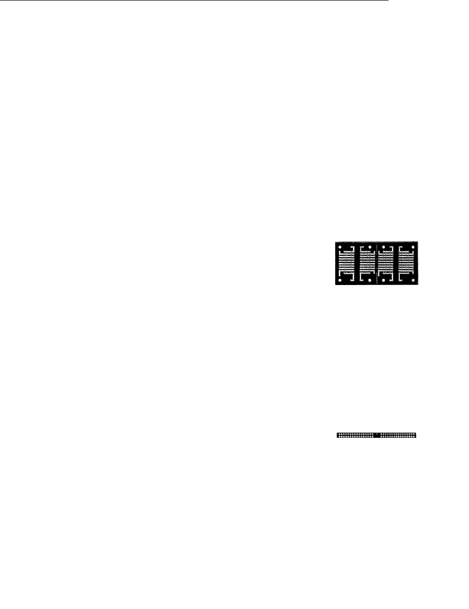
Datak
Protoboards are pre-etched with cop-
per pads and holes spaced to accom-
modated standard component leads. All,
you
need to do
is
place your compo-
nents, solder
jumper wires
i n place and'
the circuit is done.
Datak
offers
several
types
of
Protoboard.
The
one above is specifi-
cally designed for use with DIP
I C's
(catalog no. 12-607). The Protoboard'
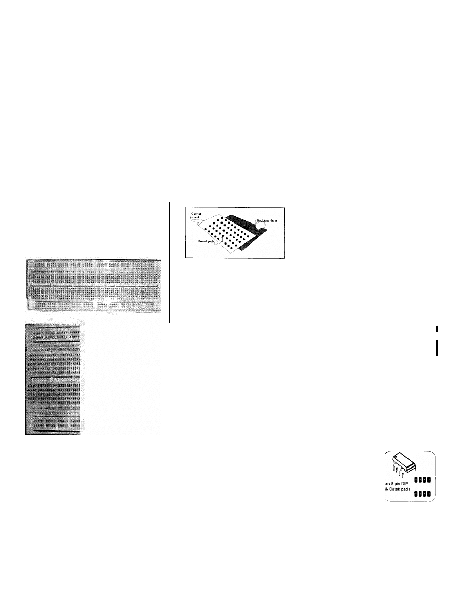
below is a general` purpose pattern with
simple copper donuts for lead wires.
................
i -a€€
..
..I
°o ...........
o .. ......°a:;,
This is universal board (catalog num-
ber 12-602) with holes and donuts set
up on 0.10" centers (as are numerous
i ndustry standard components).
puter.
These and larger Protoboards are listed'
Using Magazine
Circuits
i n the latest Philmore catalog;
Lifting a circuit from a maga- they are not yet in the Datak
zine or book is described in this sec- catalogs.
tion.
Before you use the solder-
i ng iron....
"Breadboarding" a circuit is a
term from our grandfather's days...
.. when parts were fastened to a
wooden board to see how well a circuit
would perform. To provide a quick
check to see if a given circuit would
work, parts were screwed or nailed to
a board. Wires were twisted onto ter-
minals, often never soldered.
Today we have Solderless
Prototype boards for testing circuit
i deas. Parts are simply plugged into
one of these boards with no perma-
nent connections, such as soldering.
The circuit is powered up for testing
and circuit changes are quick and
' easy.
Solderless Prototype boards
have groups of holes spaced to accept
component leads from IC's, resistors
and so on.
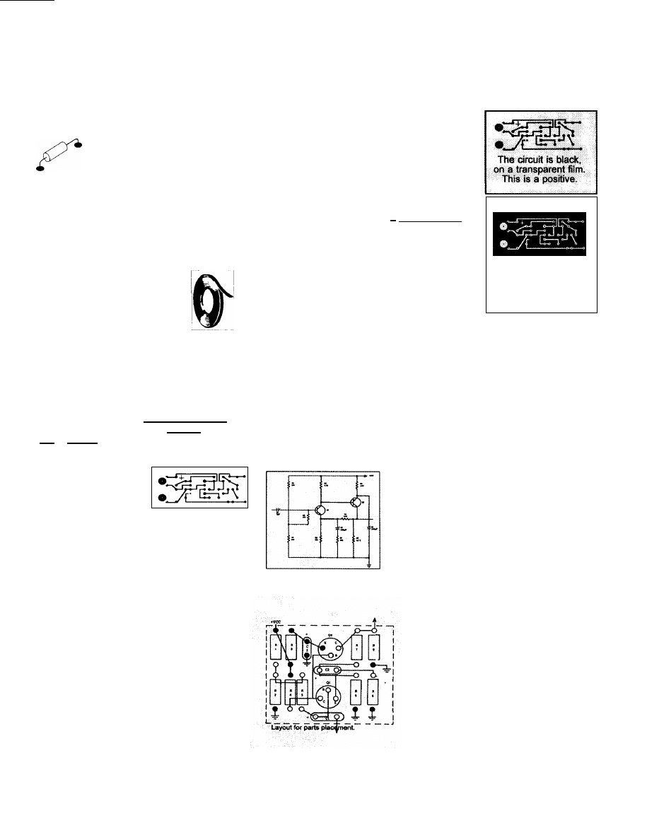
Below is a photo of a 7" wide proto-
board.
And here is a blown „
up photo of the left
end of the board.
Note the 8 pin DIP
I C and resistor.
Each pin of the IC is
i n a hole with a buss
strip that has four
other holes. You can
i nsert components
i nto these holes or a
22 gauge solid cop-
per wire "jumper".
There are several sizes of
Protoboards, ranging from small and
simple to large with binding posts for
power and output (or whatever you
want to use them for). A serious ex-
perimenter will need at least one board'
as it can help you decide if a circuit
needs changes; or may not be worth
building at all. Check the Philmore
( Datak s sister company) catalog for
details.
**
Comprehensive Datak Instructions for Printed Circuit Prototyping
Methods continued from page one.)
Etching the Board.
Whichever method you use,
you will ultimately have to etch the
board as the last step before drilling,
l oading parts and soldering. Etching, of
course, is the chemical removal of cop-
per except where your circuit is to be.
Datak provides an excellent and eco-
nomical product for this purpose. The
process is described near the end of
this booklet.
**
Direct Etch, the quickest,
cheapest method in detail.
What is a Dry-transfer? It is a sheet of
decal patterns, in this case donut pads,
on a carrier sheet. The backing sheet
protects the patterns during storage. To
place a donut from this sheet, you simply
remove the backing, place the carrier
sheet where you want a donut and bur-
nish with a blunt stick or pencil.
This section describes the use
of Dry-transfers in the direct etch proc-
ess. The Direct Etch method could be
used for massive PC boards but we
don't recommend it. As a rule of thumb,
anything larger than one or two IC's
and a transistor (with the usual list of
resistors, capacitors etc.) is probably
too big. But you decide, after reading
the following and maybe trying a small
circuit.
The Direct Etch method is
simple: Directly on the board's cop-
per surface, you mask the areas that
will become your circuit; copper not
protected by masking will be re-
moved during the etching process.
The making of a PC board could be de-
scribed as removing copper from a PC
board "blank"; and leaving behind the
copper you will want. Before etching
the board, you must protect the areas
that will become your circuit. Direct
Etch is really just a simple, accurate
masking process.
"Think Datak for your Printed Circuit Prototypes"
2
One way to protect the cop-
per would be to simply paint the
pads for IC's and resistors etc. with
a fine brush and some lacquer or
varnish. Actually this is not a bad
i dea for covering large areas to
make a ground plane; the varnish
would provide good protection
against the etchant. But what an im-
possible chore for component pads,
traces etc.!
This is where Datak prod-
ucts for Direct Etch are a terrific
apart; and the pins on each side are
on 0.10" centers. You can easily
match this
footprint
by using any
Datak
Dry Transfer
donut pads on
0.10" centers. Simply burnish onto
the copper the requisite number of
donuts:
Like this>>
Rather than
searching through
the Datak catalog
to find the pat-
terns that you will
need, consider
help. Patterns are
available for just
s
0 0
about any compo-
a
a
O
s
O
nent's footprint. And
O
0
universal donuts will
0
0
work if there is not
o
a standard pattern.
DIRECT ETCH
o
You will not need to
0
measure; spacing
0 0
0
between component
o
l eads (or contacts)
will be matched by
1111 1111
t
i
ll
the appropriate
Datak
Dry-Transfer
till
pattern. And, pre-
Sudace Mount pattern
spaced donut pat-
terns (there are
donuts
many sizes) can be
used widely for
"odd", or non-
standard compo-
nents.
an example:
DIP ("dual
i nline package")
U
I ntegrated Circuits
have two rows of
pins that are 0.30"
buying the Direct Etch Master Assortment
(no. DE-973). Included are about any pat-
tern you can imagine including
surface mount styles.
Resistors, capacitors, di-
odes and other two-leaded
devices are easy; just bur-
nish two donuts onto the cop-
per.
About the only time that things get
a little tricky is when you have a part with
no pattern. Then, measure the distance
between pins and apply a donut for each
l ead, spaced appropriately.
( Direct Etch continued.)
Once you have burnished the
component patterns
onto the bare cop-
per, connect the
pads either with dry_
transfer lines in-
cluded in the assort-
ment, or use the Etch
Resist tape which comes in tiny rolls just
li ke miniature, black masking tape.
Etch Resist tape can be purchase
i n various sizes. For starters, we suggest
two widths, the .031 "wide and .015"width.
Always use the widest that will fit, it will be
easier to handle and a better conductor.
With a finger, PRESS tape down firmly;
etchant could etch under it when it i s a -
p ie
oose y.
Here is a small circuit
with pads connected
via tape (shown 112
size).
Comprehensive Datak Instructions for Printed Circuit Prototyping
finis
Resist
tape >
When the pads and
traces have all been
applied, you are ready to etch the board
as described in the etching section of
this booklet. After etching, remove the
patterns and traces with a solvent such as
acetone, toluene, or finger nail polish re-
mover.
Direct Etch tips:
1
Use a Printed Circuit Touch-up pen to
close gaps or even for traces. The pen's ink
will
re-
sist etching if
you
get it on fairly heavily.
IBy
the way, positive artwork
is
created in the same
fashion, except that
you
place the patterns on a clear
film instead
of
directly on the copper.
*Pay
close attention to pin numbers; this
can be tricky when components are on one side and
the copper (or, circuit) on the other.
1 When using leaded components, place
the components on the side
of
the board opposite
the copper.
SMD
components have to go on the
same side
of
the copper,
of
course.
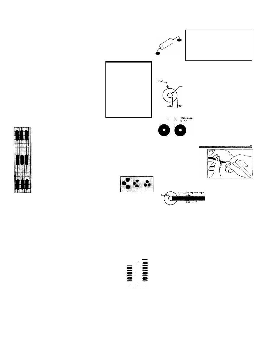
MAKING POSITIVE ARTWORK
" What is a positive?". The term positive does confuse
it is simple. A positive of a circuit is the artwork
for the circuit done in black on a clear film. The
positive (or, positive art) will look like the pic-
ture to your right. What you see in black will
eventually be copper on the board.
i mmediately below the positive is a negative of
the same circuit.
When you use Datak Dry Transfers on
clear film, you are creating a positive. OR, when
you
print a circuit from your computer's soft-
ware (In most cases; some programs do have
the ability to print a negative if you specify it).
I n
order to
make a PC board, whether you
plan
to
use a positive or negative acting
etch resist, you will need a positive to begin
with. The positive gives you the ability to make
many boards from the positive "master' and all
will be identical.
Computer software vs. drafting aids.
There can be no
question
that the computer is the
best way to produce artwork in most cases. If you will be making a multi-
l ayer board, a complex double sided board or simply a very large single
sided board, a computer
is
the answer. If you also require a component
side
silk screen plus a solder mask, the computer is the answer.
HOWEVER, there is definitely
a
cost in getting started on a computer,
which includes
a
l earning curve that may require many extra hours. If
you
only want to do an occasional board, you may find the "old-fashion"
paste-up method much easier.
If you are adept at producing a PC
layout
on
a computer, skip
the
remainder of this
section.
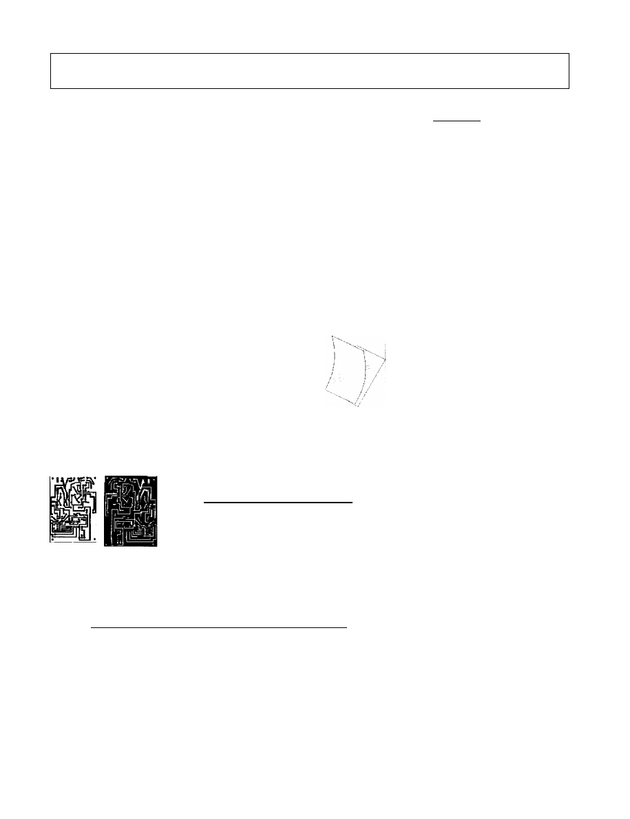
The circuit
layout:
The
simpte
two-transistor
amplifier becomes the layout
below.
3
"Think Datak for your Printed Circuit Prototypes"
people, but
A negative
-
-
negative of a circuit
i s flack background
on a transparent film;
that is: the circuit
i s
transparent, clear film.
If you
are
creating your positive "from
scratch",
you
will first have to determine the
layout for
the
PC board. Having a clear
schematic
is
one thing; converting that
schematic into a finished PC board is
some-
times quite a trick. You must determine
where each component
will
be located and
where each trace will be placed. This text is
not going to offer much help to you; circuit
l ayout is
such
a variable that we must trust
to your common sense with only the follow-
ing
tips:;
1. Usually, the schematic suggests the
PC board's layout; begin with about the
same order for major components.
2. Try to stick with a single sided
board; its easier
i n many
respects. It is
better to add a
few
wire "jumpers"
in-
stead of creating a two-sided PC board.
3. For seriously involved circuits
(i.e. large and complex), consider more
than
one
PC board, linked with ribbon
cable
or,
jumpers between sections.
4.
when you draw the layout,
have'
all
components on hand and a
caliper far measuring; specification
sheets for dimensions are helpful,
(continued)
(Making Positive Artwork continued.)
5. Draw the layout on graph paper before committing mate-
rial to circuit art (see layout above). Where to start? Usually there is
a "key" part; an IC or transistor or group of them, that should be the
center of the board. After placing them, add the resistors
and
capaci-
tors etc...
Once you have done your layout....
Making the POSITIVE ARTWORK.
Comprehensive Datak Instructions for Printed Circuit Prototyping
Note that
we are
de-
scribing making
art for
a circuit using compo-
nents
with
lead wires,
or pins.. That is
be-
cause surface
mount
i s pretty straight
for-
ward (
pie) in com-
parison.
After
you
have done this, you
can easily
handle
SMD (surface mount)
The Positive will be "built" on a
clear piece of film (like Datak # MS21). You
begin this process by placing a grid sheet
under the clear film. Then tape the two so
that they will not shift. The gird will be a
your guide, along with your layout. (Some
circuit builders do the layout on a grid
sheet and place that under the clear film).
Because components are made with leads
on 1/10 inch spacing, the grid can help you
with accurate placement of donuts. So, Step- no. 1: Place
a grid sheet on your drawing board and tape a clear sheet
on top so that the two sheets will stay together.
(Use
quality masking tape so that it will also come off when fin-
i shed.)
Step no. 2 is simply to place a donut pad wherever
there will be a component lead or pin. We suggest using
Datak
dry transfers,
if you place a pad in
the
wrong spot,
just remove by scraping with your hobby knife. Accurate
spacing for multi-pin devices such as IC's is accomplished
by both the pre-spaced Datak Donut pads
and by following your grid. Together,
they make the process very simple.
What size donut to use? You don't
need to make that decision for transistors
and DIP's such as as IC's; just use the Datak pat
tern made for that part. Note the example; shown are
patterns
for
TO-5, TO-18 and TO-92 transistors; all three leads are transferred
together with proper spacing between leads..
But for 1/4 watt resistors and small capacitors, donut size for
each lead is mostly up to you. Fairly large donuts are easier to work
with but sometimes you may be forced to use very small pads due to
space limitations. In genera for two lead components, use a donut
anywhere from .020" to .035" O.D.. You will soon get a feel for which
to use. For parts such as big electrolytics, use a donut with an inside
diameter about the same as the components lead wire. Just be sure
not to get so close to other pads that you will probably have a solder
bridge by accident.
You can even get oval "donuts" (or pads) that'
o
40
have a lead wire between them, which can be very
o
handy in tight places. The oval shape gives a small
pad . more area for the solder, producing a strong sol-
der Joint in a small place. These donut pads are on
1/10" centers, of course, so that they match the spac-
i ng of standard IC's and other DIP (dual in-line
pack-
age) devices.
The column to your right depicts some helpful; tips. Take
your time and shoot for accuracy, checking each trace
twice
When
you finish, you are ready to use presensitized positive
boards
or to
make a negative so that you can coat your own PC boards.
Transistor pads
4
Hole
Minimum
0.020°
The hobby knife, or PC
knife, is an indispensable
tool that you'll need when
making a PC board using
any method.
"Think Datak for your Printed Circuit Prototypes"
Devices with two leads will be
mounted in two donut pads.
Spacing is your decision and you
may find it convenient to run
traces for other components under
the body of the part.
Pad size: Use a size that
will surround the lead
fairly closely. (Solder will
bridge a considerable dif-
ference in hole size and
l ead diameter.) When you
can make it fit, select do-
nuts that have a minimum
of .020" between the hole
and the O.D. (outside di-
ameter).
I n general, try to
maintain at minimum 0.05"
between pads; this re-
duces solder bridges.
(Although some patterns
are much closer than this).
Try for 0.040" minimum
between traces.
ALWAYS lap tape on
top of pad to prevent
light leakage during the
exposure process
(see sketches).
POLYESTER FILM PADS
TAPE
Be sure to lap tape on top of pads.
to-
Finish the artwork by connecting
gether all pads that need to be connected.
When you cannot make a connection between
two pads that must be connected because of in-
terfering traces, consider using a jumper wire.
( Or, could you reroute interfering traces?)
Hopefully, most problems were solved during
the layout process.
Once you have finished your Positive
Artwork, you can either use it with the presensi-
tized, positive acting boards or you can create a
negative for use with the Negative acting sensi-
tizer. Both methods are described in detail in
this booklet.
Instructions for using
POSITIVE, PRESENSITIZED PC BOARDS
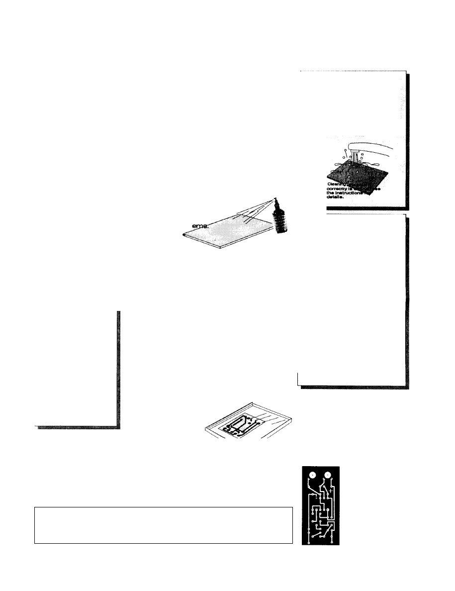
ABOUT THE DARKROOM.
A darkroom is not needed for Datak
processes; subdued incandescent
room lighting is generally good. Do
eliminate sunlight from windows and,
preferably, all fluorescent lights. We
suggest either l ow wattage incandes-
cent
lights
(25watts) at a distance of
several feet or yellow bug lights, still
kept at a distance. This whenever
handling light sensitive products
which includes Positive Boards, Neg-
Fast film or when applying or han-
dling boards that you have coated
with Datak's negative resist.
if you already have a fully
equipped dark roam, there is cer-
tainly no: harm in using it and no
problem with safe lights etc..
The WORKING AREA
and
equipment.
It is important
have a
good work area for the chemical
processes used to make PC
boards. It is necessary both to be
successful and for your personal
safety. You will need the following
for certain:
A sink
with
both hot and
cold running water; with a faucet
that will
mix
for warm as well. This
should be
in
an area that won't
mind some stains. The etchant, in
particular, can be messy and
stains are likely.
You
don't need a dark-
room, but you will need to be able
to close out sunlight (see above ).
Ventilation is important,
during etching and when using the
negative developer. In a confined
area these chemicals may cause
throat and eye irritation
and
even
lightheadedness even sickness
could result. Providing an air
flow
should prevent any reaction for
most people; use
a
fan to exhaust
fumes'
via
a
window.
Goggles are a
very
good
idea when working with chemicals;
and being close to
a
sink in case
an eye; needs
to be
rinsed
out.
ALWAYS keep the chemi-
cals
out
of reach of
young
children.
Ingestion
can be
very harmful or fatal.
POSITIVE PRESENSITIZED PC BOARDS
This is the easiest to use of the various methods, and is gener-
ally the most accurate. Although the negative method may cost you less
money, the time savings and fewer steps might compensate for material
costs being a bit higher.
What are they? The boards are conventional, 1 oz. copper PC
boards with a Fiberglas substrate. The copper is coated with a light sensi-
tive chemical that is often called a resist or a sensitizer. When this coat-
i ng is exposed to enough ultraviolet light, it will rinse away in the
developer solution, exposing the copper beneath. The copper is then
etched.
I n brief, these are the steps we are about to describe in detail:
1. Expose the PC board with your positive artwork
on top of it to UV light.
2. Develop the board in liquid developer.
3. Etching the PC board will be covered in the section
about etching.
Before we start with the procedure, we need to advise you that
there are two different types of positive board. They are very similar in
many respects, but you will want to be aware of the difference. The
Standard
series has been around for many years. The catalog numbers
for the
Standard
series always begin with a "12" (e.g. 12-024 etc.).
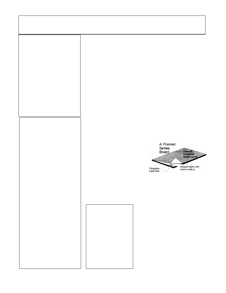
The Premier series is a deluxe version and a newer innovation. It
can be exposed with a photoflood, or even a standard incandescent 100
watt light bulb, uses less developer
and has a protective plastic, peel-off
fil m that is a big plus. The resist
coating is also superior in that small
i mperfections have been reduced to
almost nonexistent (very rarely need-
i ng touchup after developing). The
Premier series is somewhat more
costly (average 15-20%).Premier
boards have part numbers beginning
with the numeral "14" (e.g. 14-024
etc. )
The two biggest advantages in using the Premier series are the
higher quality coating and the plastic film protective cover. While this
peel-off cover is in place, you can measure, mark and cut the board to
size in normal room lighting, even bright lighting. Standard boards must
always be handled in very subdued light.
Confusing Terminology.
The industry tends to use
several terms for "Positive-
acting PC boards". A posi-
tive board
i s
a positive board
and do not be distracted by
variations such as "positive
acting",
"pre-sensitzed" or
coated etc.. And the terms
Precoated
and
Presensitzed
are interchangeable as are
resist
and
sensitizer.
Technically, the coating is a
resist and not a sensitizer,
the resist is light sensitive.
The term "positive" is the
giveaway
However, Standard boards should not
be considered to be terribly inferior; they
have been the industry's mainstay for
nearly two decades and can be counted
upon for very good results. Here are the
main differences
>Standard boards require UV light for
exposure, Premier boards do not.
>Standard boards, mix developer with
three parts water vs. ten parts water for
Premier boards.
>Standard boards should be checked
after developing for possible touchup be-
fore etching; they may need just a dab
with your PC ink pen.
( Continued next page)
Instructions for using POSITIVE, PRESENSITIZED PC BOARDS.
Your positive
will
be placed
on top of the resist coating
on the copper side of the
PC board during exposure.
Be sure that the positive is
not upside-down; the cir-
cuit in copper is going to
be oriented the same way
as your positive on top of
the board.
Step 4. Expose
the board with your
positive. Follow the
Exposure Chart for
exposure time. Use
an exposure frame.
Place your posi-
tive on top of the sen-
sitized coating on the
PC board and sand-
wich the two in the
exposure frame.
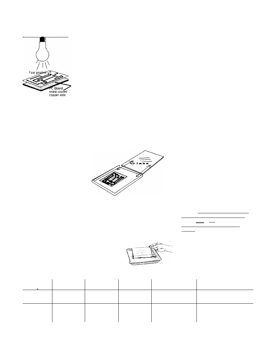
The Exposure Frame: This device will be familiar to you if you
have ever made photographic prints. The frame is simply a holder for a
small board and piece of glass. With your positive in place on top of a
precoated board, put the two in the frame under the glass and slide into
the frame. The frame will hold the two tightly together for two reasons:
(1.) the positive should never move around during exposure and (2.) the
positive is pressed tightly against the board so that light does not get un-
der the positive. Now expose to
li ght.
The Light Source:
See the chart at the bottom
of this page. We are assuming
that your line voltage is be-
tween 115 and 125 Volts AC
.. if below this range, you may
have problems. Also, for the
sun, keep in mind that its ul-
traviolet output could vary; es-
pecially in large cities, on hazy
days etc. .
Note that the Premier
series can use an ordinary 100
watt white incandescent light bulb.
Develop the board: While the board is being exposed, prepare a tray of
developer solution. Mix the Datak developer concentrate 1:10 with water
for the Premier series; or 1:3 for the
Standard
series. NOTE carefully;
mix with very warm water. A cold developer is not going to work, it
should be above room temperature or warmer. (Be sure to use only
Datak nos. 12-402 or 12-406.)
Use glass/plastic photographic tray.
Use just enough developer to cover the
board. Rock the tray gently until the copper
i s fully exposed in areas to be etched. It will
be obvious to you when the copper is bare;
be sure that there is no haze or film remain-
i ng. Rinse in cold water for a couple of min-
utes. (Continued next page.)
The exposure
frame; holds the
postive firmly
against the PC
board during
exposure to light
**
l ook for desklamps that hold two bulbs
*sun about noon to two P.M.
6
TINNIT©
Tin
Plating
for
PC
boards.
Kit no. 12-800
This is a slick product
that should be of
particular
i nter-
est to professional users. When
you get to the point where you
have a finished PC board, you
may
want to tin
plate the copper
for two
or
three reasons.
The tin plate, which sol-
ders very easily, looks very sharp,
shiny and clean. If you are mak-
ing a board for a customer, tin
looks quite professional. And the
look lasts.
TINNIT will also provide
protection for boards that will be
stored for later use; they will re-
main solderable and the copper
will be protected.
I NSTRUCTIONS
TINNIT
is electroless, re-
quiring no electrodes or wires.
NOTE: WE RECOMMEND
GOGGLES and RUBBER
GLOVES WHILE' WORKING
WITH THIS PRODUCT.
1. Dissolve the TINNIT
powdered concentrate (marked
no.
ER-18)
in
12 ounces of very
warm water (temperature about
130°
F)
and'
then add water to
make one pint (16oz.).
NOTE: Use only a plastic
or glass contaner
or mixing an
or storage.
o not use metal
containers or caps With meta llic
li nings.
2. Prepare the circuit
board for plating by removing all
traces of resist with either ace
tone, lacquer thinner or
DATAKOAT® thinner. If oxides
are present, clean with scouring
powder rather than soap or deter-
gent; do not use steel wool.
Continued on page seven)
Board
T type
F1 5 T 8-BL
X2 bulbs**
app. noon
SUN*
Datak ER-39
bulb
mix
developer
concentrate
i 00 watt bulb
Premier onl
STANDARD
R
12 to 14 min.
8 to 10 min.
12 to 15 min.
3 parts water to 1
not applicable
@ 7 inches
any distance
@12 min.
PREMIER
9 to 12 min.
4 to 4.5 min.
10 min.
10 parts water to 1
10-12minutes
@7"
12" distance
@12" distance.
Positive Boards continued ..... and Making a Negative from a Positive with
Neg-Fast
Film.
Etching: Your are now ready to etch the board; see the sec-
tion on etching later in this booklet. After etching, you will be ready to
drill the board and mount the parts, solder and finish the circuit.
Final notes: Here are some helpful tips for users of the posi-
tive PC boards:
1. Store used developer in a plastic or glass bottle. Plastic is
best as you may squeeze most of the air out of the bottle and cap
tightly. Do this because the developer will react, over time, with the
carbon dioxide in the air and decompose.
2. You can use the developer until it simply does not perform;
then flush it down the sink with a fast cold water chaser. Storing de-
veloper in a refrigerator can help to keep it fresh for very long periods.
3. We suggest leaving the resist on the board until after drill-
i ng. Remove the resist with solvents including acetone or a non-
acetone fingernail polish remover. The later is available at most drug
stores and discount stores.
4. IF the board proves to be tough to etch, you probably did
not develop it long enough and some resist residue remained behind.
Or, said residue can also be caused by too short an exposure time,
too weak a light source and so on.
Making a Negative from a positive or a
Magazine page circuit.
Neg-Fast
fil m is a product that will help you
to easily create a negative for use with the Negative
Photo Resist Spray from Datak or any other negative
acting resist.
Neg-Fast is
a plastic sheet, about as
thick as a sheet of paper. It is available in small sheets
5" X 6" or larger sheets 11" X 8". When exposed to light with your
positive and then developed in a special liquid, a negative is produced.
The process is simple and very reliable.
I NSTRUCTIONS:
Handle
Neg-Fast
fil m in very subdued light
and with no sunlight or fluorescent light pre-
sent. It is also OK to use yellow light.
For use with a magazine arti-
cle/circuit:
Step 1a. IF the circuit has no printing
on the reverse side of the page , you can clip
i t from the magazine. Or, you can use an of-
fice photocopier and make a copy. Make a
a negative on the right.
good, high contrast copy with the circuit
plenty dark, other areas white.
Step 2a. A printed magazine clipping or pho-
tocopy such as this requires an exposure time of four minutes at a
distance of 24" using the Datak no. ER-39 bulb. Except for this expo-
sure time, follow the steps as given below.
For use with a pasted up or photographic Positive.
(This is a positive circuit on a transparent film.)
Step 1. Use scissors or a sharp PC knife, cut the film to a
size matching your circuit positive (or a bit larger).
Step 2. Place the film in an exposure frame with the emulsion
side up*.
the positive on top of the film (the positive can acei-
ther direction, there is no "right-side-up".) Close frame securely.
(Continued next page)
A positive on the left,
000
(continued from page six.)
Remove all cleanser residue by
washing thoroughly i n plenty of clean
water: If you
o no thoroughly re-
move all cleanser and etch residues,
they can seriously deplete the TINNIT
bath.
3. Place the TINNIT solution
i n
a
Pyrex tray and heat to between
120 and 140 degrees F. Immerse the
board for between 10 and 30 minutes.
Agitate for
a
moment at five minute
i ntervals. A bright tin plating
will
re-
sult.
4.
Rinse the board with run-
ning tap water and_
dry
with paper
towels.
Special
notes:
If the TINNIT solution is left
standing it may evaporate, leaving - a
precipitate (white
or
li ght yellow).
The precipitate will again
dissolve
when
water i s added and heated and
i s
perfectly
usable.
Do not leave, powder residue
to heat on stove; heated dry salts can
decompose and' release very irritating
sulfur dioxide and ammonia gases.
TINNIT may be stored for
about six months (longer if refriger-
ated) in an airtight bottle made of ei-
ther plastic or glass. Avoid metal
bottle caps.
TINNIT WARNING: This
product contains acidic tin salts.
Although it contains no cyanides or
other highly poisonous materials, it is
a skin and eye irritant. In case of eye
contact, flush immediately with run-
ning water. Consult a physician as
soon as possible.
I F ingested, do not induce
vomiting. Call a physician. Drink
plenty of water, as much as possible.
Never leave these chemicals
i n the reach of children. Younger
teenagers should be supervised by a
knowledgeable and responsible adult.
Neg-Fast
Film continued.
(continued from page seven)
Step 3. Expose to the Datak ER-39 bulb at a distance of 24" for
1-1/2 minutes (4 minutes if a paper positive).
Special note: For circuits larger than 4" X 4", you may find the outer
comers not fully exposed. For larger boards, you may suspend the
ER-39 bulb
so that it swings freely on its power cord. During a five minute exposure time,
keep the
bulb
gently swinging
randomly back and
forth across the board which
is in its exposure frame about 24" directly below the bulb. Use
a
porcelain
socket as it can take the heat.
Step 4. Use only as much developer as needed; do not return used
developer to the bottle. Mix the developer concentrate with four parts of very
warm tap water. Place the developer in a shallow tray (either glass or plastic,
not metal). Develop for about two minutes; or until you can see that you have a
good clear image of the circuit's negative. The developer's temperature should
be warm, not less than about 72 degrees F but not above about 90 degrees.
When fully developed, gently rinse in lukewarm tap water.
Step 5. Mix one part of the Fixer concentrate with 4 parts of warm tap
water and allow the negative to stand in this solution for about five minutes. (If
you are using the developer tray, be sure to rinse it out with water first.) It is
necessary to use only enough to cover the film but you may return unused fixer
to the bottle. (When it comes to the time to buy new developers, throw away
this old fixer as the developer package comes with new fixer too.)
Step 6. Rinse again in fresh, warm tap water and place gently between
a couple of paper towels to absorb excess moisture. You may then dry by leav-
i ng it on top of another, fresh paper towel or hang it with a film clip. You may
use warm air or heat to hurry the process, but do not exceed 122 degrees
Fahrenheit or you
will
distort the film.
Step 7. Touch up may be done with a black pen such as Datak nos.
ER-15 or extra fine point ER-25. Eliminate any
pin hole spots, if any.
Step 8. Finished. Use the negative
with a PC board coated with Datak no. ER-71
sensitizer or with other maker's negative-
acting PC boards.
Exhausted fixer and developer may
be flushed down the drain; follow up with a
couple of minutes of fast run-
ning cold water.
Use a shallow photo-
graphic tray (glass or
plastic) for developing
and fixing ; use just
enough developer or
fixer to fully cover the
film.
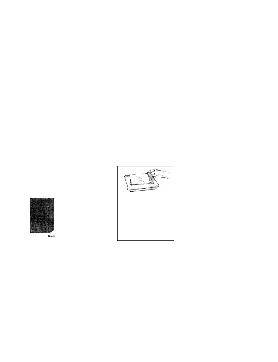
`Identifying the emulsion
side of the film.
Each sheet of film will
have a notch along one
edge. Hold the sheet up
i n front of you; when the
notch is on the bottom
edge and closest to your right hand, the
emulsion side is facing you. OR, simply scratch each side with your PC
knife tip. The emulsion side will scratch away revealing a clear film; the
non-emulsion side will not show scratches.
TIPS & MISCELLANY
Computer Software ... if you
are
considering a computer program for
drafting your PC board layouts,
PCDATAK may be a good choice.
It is a DOS program but can run
under Windows or Wndows95. It is
very
l ow
cost, easy and quick to
l earn and incredibly flexible for a
l ow
cost program. To print circuits,
you need to have a LaserJet printer
with the Postscript feature. Or, take
the circuit on diskette to Kinko's as
they have such printers. Datak's
catalog number for the software is
12-077.
Soldering ... PC circuit layout de-
scriptions in this booklet are as-
suming that you will be hand
soldering your final circuit board. If
your prototype will eventually be a
production item and you are plan-
ning to use dip or wave soldering
equipment, then circuit layout
needs to be done accordingly. This
booklet does not go into enough
depth'
to
teach techniques for true
production boards.
For production, use a
software to do your layout. Most
programs incorporate accepted
techniques that will keep you out of
trouble. Datak's software,
PCDATAK no. 12-077 automatically
provides correct spacing between
traces, donuts etc..
Drilling the PC board ... drilling with
a standard, household hand drill
can be an excruciating chore; and
it is very difficult to do a decent job.
We suggest that you use only a
drill press, even if you have to beg
a neighbor to use his. If you use a
hi-speed mini-drill such as those
from Dremel, use a light dimmer to
slow it down about 40%. (You will
get a feel for the right speed after
using it
for
a short time.) A slowed-
down Dremel with a Dremel drill
press' is the ideal way to drill your
boards.
Small bits are available
from Datak and also from most in-
dustrial
supply
houses which will
carry dozens of sizes.
The Negative Acting Photo Resist method
NEGATIVE PHOTO RESIST
for PC
BOARD MAKING
The method is based upon using the Datak no. ER-71 Photo
Resist liquid, which is a light sensitive spray-on resist. The small, 4 ounce
bottle will cover about 1,700 square inches and is applied with the pump
action sprayer included in the package. Good results can be expected if
you carefully follow the steps.
You will need to begin with a quality negative. If you have
a positive, see the section on using NegFast film to produce a negative.
Or, use standard photographic process to make a high contrast negative.
Step 1. Clean the PC board. This is a critical step and must be
done well. Scour the board with water and a common kitchen cleanser
(containing bleach) and very fine steel wool. Scrub the board and rinse
until water sheets out evenly over the entire surface when you hold the
board horizontally under a pencil-lead
stream of water. If the water tends to
pull away from the boards edges or
any point on the aboard, clean it
again. If the board cannot pass this
water test, it is "dirty" and must be
cleaned until it passes.
Dry the cleaned board with
paper towels. You could wipe with am-
monia (never with alcohol). Handle by
the edges, don't touch the surface.
Step 2. Coat the Board with Resist. Do in subdued light* The
board should be warm, ideally about 120 degrees F. Heat the board on a
hot plate or you could warm it with a heat gun or hair dryer.
Lay the board flat and spray a light, continuous
film . (Sink marks will indicate poor board
cleaning.) Sight along the board surface toward
your light; make the coat as even as possible.
Drying the board in
a dark cupboard
works fine if there is
plenty of volume in
the cupboard. But if
the volume is quite
small, there is
sometimes not
enough air to absorb
the fumes and the
board takes a very
l ong time to dry.
Don't expect a small
drawer to dry two or
three boards over-
night.
Step 4. Exposing the PC Board. Place your
negative on top of the resist coating and place
the two in a contact
exposure frame.
The frame
will hold the negative and board tightly together
to prevent light from leaking between them.
Expose the board to light using one of
the following choices:
Spray a thin, even
coat. Thick coats
may cause
probl
Step 3. Drying the PC Board. The board
may simply be place in a dark cupboard to dry
over night. Or, bake it in an oven at 140 de
grees F for twenty minutes; the oven must be
dark. Allow the board to cool ten minutes be-
fore use.
I f your coating is not a clean looking,
even coat with few signs of bubbles, consider
repeating the proc-
ess by adding a sec-
ond coat. Strive for a
thin coat, and as
even as you can
make it.
The exposure frame
clamps the positive or
negative tightly against the
PC board; and the glass
top allows exposure to
light.
* subdued
light. After you clean the board and until you finish the develop-
i ng stage, work only in subdued lighting such as a 25 watt bulb several
feet away or a yellow "bug" light bulb.
Sometimes steel wool will
contain oil; but it can be re-
moved with some soap and
running water. Soap,
squeeze and rinse a pad two
or three cycles and it will be
clean
enough to use. A liquid
dish
soap is suggested.
Spraying the board is an
i mportant step; try to get a
thin and even coat. A thick
coat can result in ragged
edges on pads and traces in
your finished board.
tip: Pump the spray fully, do
not try to squirt a light coat
by
pumping
with
short
strokes. Start spraying off
the edge of the board and
sweep across the
board;
each pump cycle should be
a full stroke. (Short strokes
tend to shoot globs, which
are not good.)
Always spray on a
warm board; a board that is
cool is very tough to coat
properly. Some users let the
board dry and apply a sec-
ond coating.
The negative is clear (trans-
parent) where there will be cir-
cuit and the "background" is
opaque.
You can make a
negative using
Datak Neg-Fast
film or photo-
graphically. Also,
some software
will make a
negative of a PC
board layout.
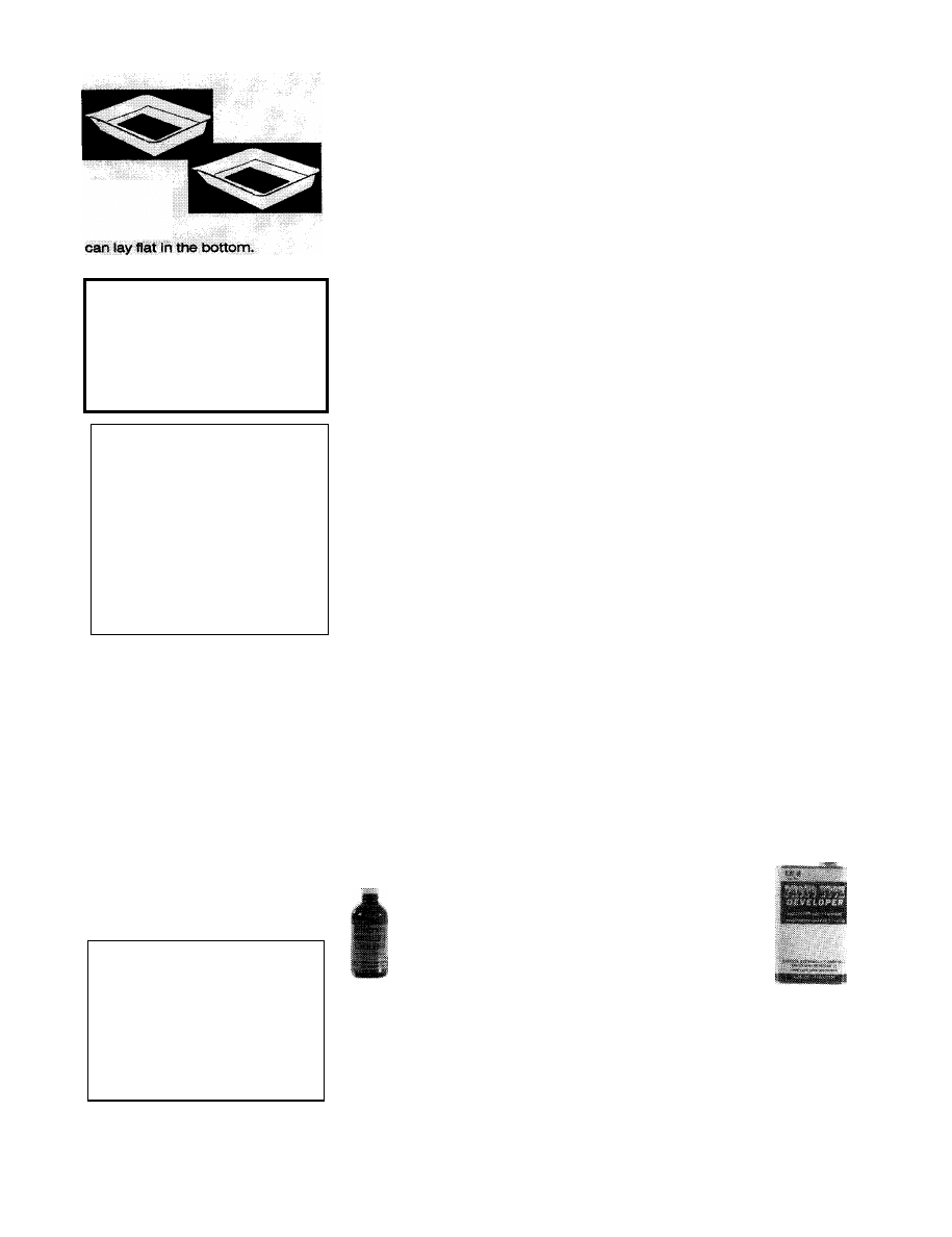
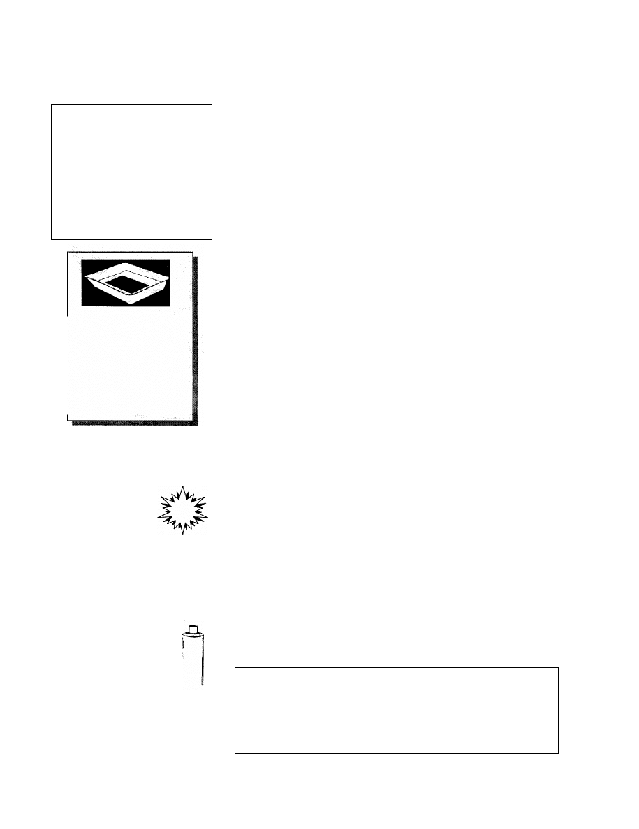
Developing
trays should
be large
enough that
the PC board
Ragged edges on the resist
image mean that the resist
was not completely dry be-
fore the exposure, OR, that
the resist was applied too
heavily and should not have
been such a thick coating.
Spread-out lines occur if you
exposed too long or If the
negative was not in perfect
contact with the PC board.
This can happen if you use a
warped board. If the pattern
i s bad, you may as well sal-
vage the board by cleaning
off the resist with lacquer
thinner and clean-
I ng/recoating. (A warped
board can usually be gently
bent into shape.)
The Datak ER-8 Developer
contains aromatic, partially
chlorinated hydrocarbons. The
product can attack plastics
and may discolor vinyl counter
tops, attack wood finishes and
so on. In addition to the pre-
cautions listed on the pack-
age, don't use this product in
areas that can't stand some
abuse.
Never leave such chemicals
where children might get Into
them. Ingestion of this and
other PC board making chemi-
cals
can be very harmful and
even fatal, especially in small
children.
Fast removal of all
manner of etch resists can
be done with an acetone
free fingernail polish re-
mover. It can be found near
the fingernail polish in drug
stores and discount stores
etc.. It is a cheap and effec-
tive way to go.
(Negative Photo Resist ..... continued from previous page.)
1.) Sunlight at about noon, for three minutes.
2.) Datak no. ER-39 bulb, for 5-1/2 minutes at
a
distance of 20".
3.) Two F15T8BL bulbs 20 minutes at 15".
Step 5. Developing the PC Board...
You need two metal or glass photo-
graphic trays for developing (never use plastic
rtrays). If you work with small boards, find some
smaller trays which will save on developer.
Use only Datak developer no. ER-8. Place enough developer in each tray
so that the board is under the developer by about 1/16" when it is placed
flat in the tray.
Note: The resist pattern is transparent during developing and can-
not be seen until it is completely dry.
Follow these developing steps:
a.) Place exposed board in first tray for 30 to 45 seconds, gently
rocking the tray every five seconds. (Never touch the surface of the
board, the resist will scratch easily. Handle by the edges.)
b.) Remove board, holding by the edges. Allow it to drain for ten
seconds and then place it face down on 2 or 3 layers of clean facial tissue
(don't slide or rub!).
c.) Carefully remove tissue and immerse the board in second tray
for ten seconds. Remove, allow it to dry and inspect the pattern against
the light (hold board flat and point it toward the light; sight along board).
Good developing shows up the pattern clearly with no drain marks or
stains in the areas to be etched. Old, used developer will leave globs at
random.
Dry thoroughly before etching; at least ten minutes at room tem-
perature. The resist must be hard before etching.
Step 6. Touch up. The board may now be handled in normal lighting.
I nspect the board for breaks in traces or pads. If there are any, you can
touch them up with the etch resist pen. Repair any breaks before etching.
I f the above steps were done well, touch up will probably not be needed.
Etch the PC board. (See section about etching.)
00*
The Products...
( Continued on next page)
The no. ER-71 Photo Resist (left) is supplied in
a
dark bottle which
will
prevent deterioration.
Officially, the shelf life is about two years; but the
actual life is probably much longer. It can be
stored at room temperature; cooler temperatures
will add to the shelf life. Warm it up to at least
room temperature to apply it. The Resist has a
spray cap for application. Spin coating is also
good if you are equipped to do it.
The no. ER-8 developer
i s
supplied in
a
metal can and
will
keep for a long time if kept
tightly shut. If you plan to do quite a number or
boards, then
you'll
want to start with two cans. The
Resist
will
cover about 1,700 square inches of copper but
a
can of developer won't develop nearly that much area. (Area
will vary with circuit density.)
10
THE WORK AREA
SHOULD BE WELL
VENTILATED; AVOID
BREATHING VAPORS
and avoid skin contact.
Do not use near open
flames or sparks.
Ferric Chloride etchant
can stain clothing (and just
about anything else) horri-
bly. Wear old cloths and
don't use this in an area
that can't take some
stains. Work close to run-
ning water; an immediate
cold water flush can re-
duce staining, rinse out an
eye etc..
Etching can be done
i n
an
open, photo-
graphic tray. If you
keep the tray covered
with a piece of window
glass when not in use,
i t
will
reduce the
fumes and can be
kept this way for many
hours.
NEVER add water to the
Etch Powder Concentrate!
Add the powder to water.
HEATING &
Boiling !!
The mixing of water with
Ferric Chloride powder gen-
erates considerable heat.
You must add the powder to
the water;
NEVER
add wa-
ter to the powder!
Used ferric chloride
etchant may be
stored in plastic bot-
tles for future use. If
you will be storing it
for quite awhile and
the bottle is not full,
squeeze the bottle to
eliminate most of the air
space. It should last many
months.
ETCHING PC BOARDS
The ETCHING PROCESS.
There are any number of chemicals that may be used as an
etchant. The only one that we recommend is Ferric Chloride. It is available
from some sources as a liquid and Datak supplies it in powder form to be
mixed by the user with water. This is the most effective and economical of
the etchants.
Factors that will accelerate the ferric chloride etching process are
heat, oxygen and agitation. The etchant will work at room temperature but
at higher temperatures (say, about 125 degrees F) it will work much faster
and cleaner. Agitation not only keeps moving fresh developer over the
copper, but introduces oxygen, which acts something like a catalyst.
Ferric Chloride is not an acid; the chemical process is one of dis-
placement. We do not recommend acids for many reasons of safety and
effectiveness, disposal problems etc..
The etching container must be either glass or plastic. It can be as
simple as a photographic tray (that you keep rocking gently) to the Datak
etching tank, which bubbles air through the solution to provide both agita
tion and oxygen. A fish-tank type heater adds to the effectiveness of the
etch tank. Agitation is very important and proper etching won't happen
without fairly constant of the etchant during the entire process.
Using Datak Ferric Chloride ..... We always recommend that you
Wear eye protection and provide adequate ventilation. The fol-
l owing assumes that you will use an open, photographic tray. Mixing is the
same regardless of what devices you use during etching, i.e. the etching
tank, tray etc..
Step 1. Mix a package of Datak number ER-3 ferric chloride pow-
der with 16 ounces of water. Add the powder slowly; expect heating of the
water as you go. Adding too fast can cause splattering due to the fast
heating. An empty, plastic one gallon milk jug works fine for the process.
Mix until all powder is dissolved. Then store the finished product in a plas-
tic bottle. It will keep for a long time.
Step 2. Preheat the etchant. You could preheat the etchant by im-
mersing its storage bottle in a bucket of hot water for twenty minutes be-
fore pouring it into a tray. IT WILL EXPAND WHEN HEATED, LOOSEN
THE BOTTLE CAP SO THE BOTTLE WON'T BURST. Or you could use a
Pyrex glass tray on a low-heat hot plate (etc.). A heat lamp could be used
on an open tray. Room temperature will work, but slowly.
Step 3. Etching can take from ten to twenty-five minutes. Immerse
the PC board and continue agitation by rocking the tray gently, or lifting
and immersing the board with a plastic tweezers etc..
Step 4. Inspect the board periodically and it will be obvious when
etching is complete. When finished, rinse the board with fresh water, wipe
off with paper towels. The process is completed and you are ready to drill
the board, remove the resist and load the parts.
You may pour used etchant back into the container to use it again.
Replace the etchant when the process slows down considerably. Old
etchant may be flushed down the sink but be sure to follow-up with a vig-
orous water chaser for two or three minutes. The etchant will dilute and
disperse quickly.
Users note: Ferric Chloride etchant is available from several
sources. Some is not of good quality and you will note that it is
slow to act and etches only a very small volume of copper. Datak
provides a very high quality etchant and at a price that is better
than some of the lower grade materials. We do strongly urge you
to use the Datak product. Slow etching can cause undercutting,
weakened resist and other problems.
Wyszukiwarka
Podobne podstrony:
(ebook pdf) How to Make Love All Night (and Drive a Woman Wild)
(Ebook Survival) How To Make Emergency Gas Masks(1)
[EBOOK] How to Make Wine at Home Tips and Techniques
ENERGY POWER WATER Electricity How to Build a Waterwheel Generator (ebook Home Power Diy 185336
(ebook pdf) How to Set Your Electric Guitar Up Properly
ebook How To Make Wine At Home
How to Make Wine At Home (eBook)
How to Make Wine At Home (eBook)
How to make
How to make an inexpensive exte Nieznany
How to Make an Atomic Bomb
How To Make It And Enjoy It
how to make a draino bomb 6W5PMX3CSBHVWUCD22KIJY34P667TPDLPPATGOY
how to make a?ke id D5O42G7A4RE7MNTMEISZ7BJSGUVLODZANAC376Y
więcej podobnych podstron