1/6
LIS2L02AS
December 2002
This is preliminary information on a new product now in development. Details are subject to change without notice.
■
3V TO 5.25V SINGLE SUPPLY OPERATION
■
THE SENSITIVITY IS ADJUSTED WITH A
TOTAL ACCURACY OF ±10%
■
THE OUTPUT VOLTAGE, OFFSET,
SENSITIVITY AND TEST VOLTAGE ARE
RATIOMETRIC TO THE SUPPLY VOLTAGE
■
DEVICE SENSITIVITY IS ON-CHIP FACTORY
TRIMMED
■
EMBEDDED SELF TEST
■
HIGH SHOCK SURVIVABILITY
DESCRIPTION
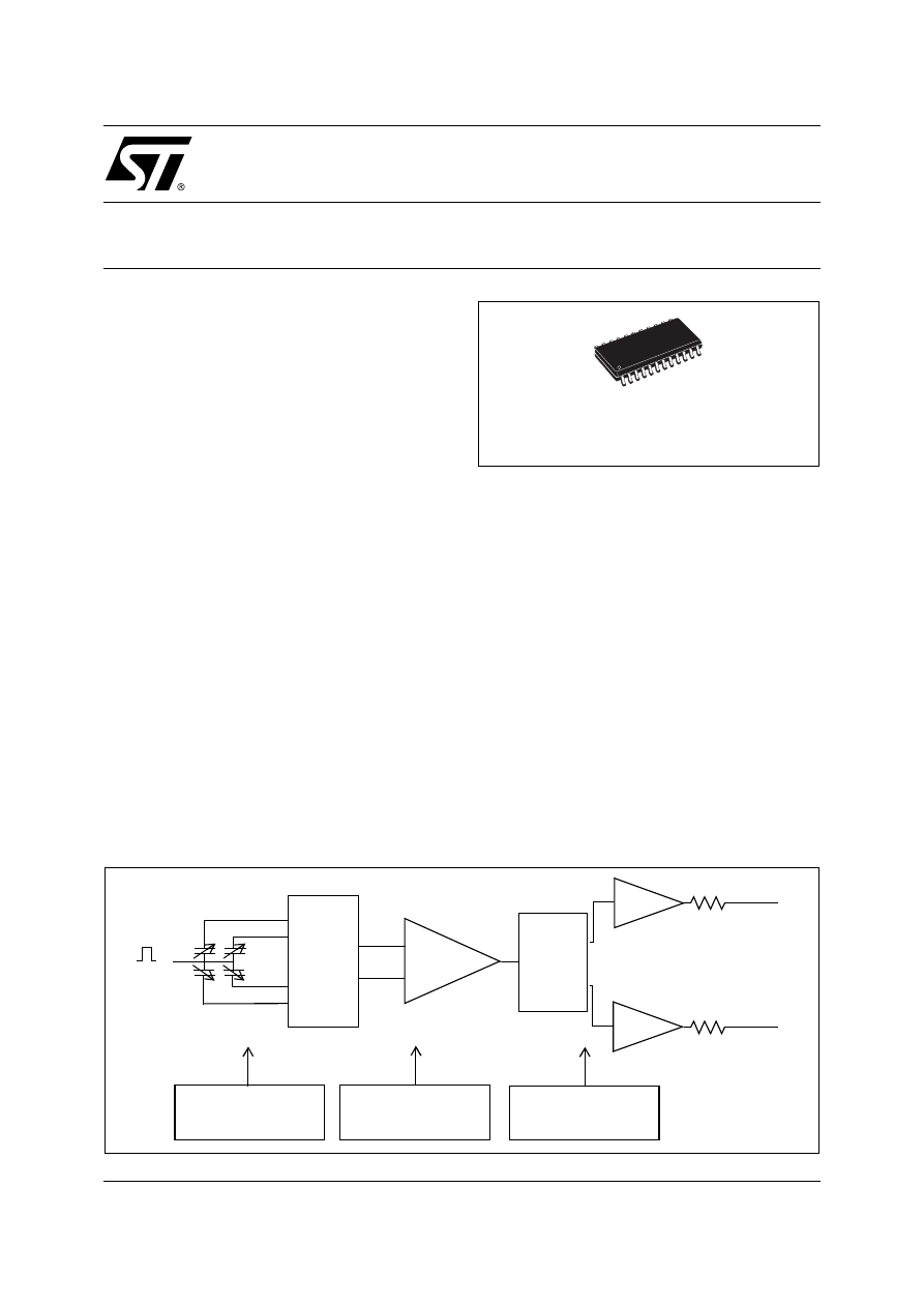
The LIS2L02AS is a dual-axis linear accelerometer
that includes a sensing element and an IC interface
able to take the information from the sensing element
and to provide an analog signal to the external world.
The sensing element, capable to detect the acceler-
ation, is manufactured using a dedicated process
called THELMA (Thick Epi-Poly Layer for Microactu-
ators and Accelerometers) developed by ST to pro-
duce inertial sensors and actuators in silicon.
The IC interface instead is manufactured using a
CMOS process that allows high level of integration to
design a dedicated circuit which is trimmed to better
match the sensing element characteristics.
The LIS2L02AS has a user selectable full scale of 2g,
6g and it is capable of measuring accelerations over
a maximum bandwidth of 4.0 KHz for both the X and
Y axis. The device bandwidth may be reduced by us-
ing external capacitances. A self-test capability al-
lows the user to check the functioning of the system.
The LIS2L02AS is available in plastic SMD package
and it is specified over a temperature range extend-
ing from -40°C to +85°C.
The LIS2L02AS belongs to a family of products suit-
able for a variety of applications:
– Antitheft systems
– Inertial navigation
– Virtual reality input devices
– Vibration Monitoring, recording and compen-
sation
– Appliance control
– Robotics
SO-24
ORDERING NUMBER: LIS2L02AS
PRODUCT PREVIEW
INERTIAL SENSOR:
2Axis - 2g/6g LINEAR ACCELEROMETER
BLOCK DIAGRAM
DEMUX
S/H
CHARGE
AMPLIFIER
S/H
MUX
S1X
S1Y
S2X
S2Y
Voutx
Vouty
Routx
Routy
rot
VOLTAGE & CURRENT
REFERENCE
TRIMMING CIRCUIT
&
CLOCK
&
PHASE GENERATOR
TEST INTERFACE
LIS2L02AS
2/6
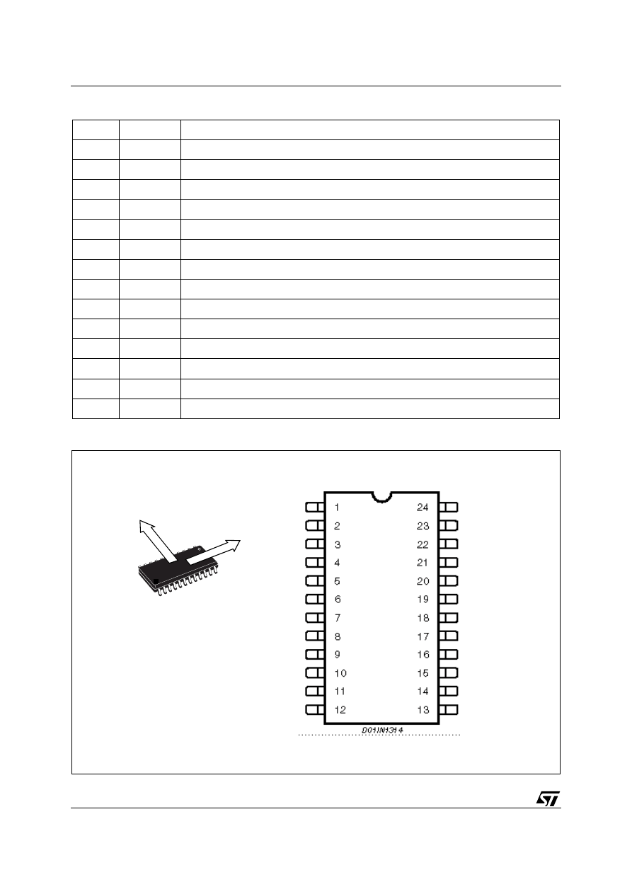
PIN DESCRIPTION
PIN CONNECTION (Top view)
N°
Pin
Function
1 to 6
NC
Internally not connected
7
Reserved
Leave unconnected or connect to ground
8
Reserved
Leave unconnected or connect to Vdd
9
Reserved
Connect to Vdd or ground
10-11
Reserved
Leave unconnected or connect to Vdd
12
FS
Full Scale selection (Logic 0: 2g Full-scale; Logic 1: 6g Full-scale)
13
NC
Internally not connected
14
PD
Power Down (Logic 0: normal mode; Logic 1: Power-Down mode)
15
Voutx
Output Voltage
16
ST
Self Test (Logic 0: normal mode; Logic 1: Self-test)
17
Vouty
Output Voltage
18
Vdd
Power supply
19
GND
0V supply
20 to 24
NC
Internally not connected
NC
NC
NC
NC
NC
GND
Vdd
Vouty
ST
Voutx
PD
NC
NC
NC
NC
NC
NC
NC
Reserved
Reserved
Reserved
Reserved
Reserved
FS
DIRECTION OF THE
DETECTABLE
ACCELERATIONS
Y
1
13
X

3/6
LIS2L02AS
ELECTRICAL CHARACTERISTCS (Temperature range -40°C to +85°C)
1
FUNCTIONALITY
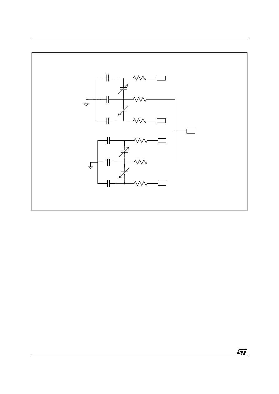
1.1 Sensing element
The THELMA process is utilized to create a surface micro-machined accelerometer. The technology allows to
carry out suspended silicon structures which are attached to the substrate in a few points called anchors and
free to move on a plane parallel to the substrate itself. To be compatible with the traditional packaging tech-
niques a cap is placed on top of the sensing element to avoid blocking the moving parts during the molding
phase.
The equivalent circuit for the sensing element is shown in the below figure; when a linear acceleration is applied,
the proof mass displaces from its nominal position, causing an imbalance in the capacitive half-bridge. This im-
balance is measured using charge integration in response to a voltage pulse applied to the sense capacitor.
The nominal value of the capacitors, at steady state, is few pF and when an acceleration is applied the maximum
variation of the capacitive load is few tenth of pF.
Symbol
Parameter
Test Condition
Min.
Typ.
Max.
Unit
V
dd
Supply voltage
3
5.25
V
I
dd
Supply current
1.0
mA
V
off
Zero-g level
T
amb
= 25°C
ratiometric to Vdd
V
dd
/2-10%
V
dd
/2
V
dd
/2+10%
V
A
r
Acceleration range
0V on FS pin
±
1.8
±
2.0
±
2.2
g
V
dd
on FS pin
±
±
6.0
g
S
o
Sensitivity ratiometric to
V
dd
T
amb
= 25°C
Full-scale = 2g
V
dd
/5–10%
V
dd
/5
V
dd
/5+10%
V/g
T
amb
= 25°C
Full-scale = 6g
V
dd
/15–10%
V
dd
/15
V
dd
/15+10%
V/g
N
L
Non Linearity
Best fit straight line
X, Y axis
Full-scale = 2g
±
0.3
%
f
uc
Sensing Element Resonant
Frequency
X, Y axis
4.0
KHz
a
n
Acceleration noise density
V
dd
= 5V
Full-scale = 2g
50
µ
g/
V
t
Self test output voltage
Ratiometric to V
dd
T
amb
= 25°C
@ 5V
100
mV
V
st
Self test input
Logic 0 level
0
0.8
V
Logic 1 level
2.8
V
dd
V
R
out
Output impedance
100
k
Ω
C
load
Capacitive load drive
320
pF
Hz
LIS2L02AS
4/6
Figure 1. Equivalent electrical circuit
1.2 IC Interface
The complete signal processing uses a fully differential structure, while the final stage converts the differential
signal into a single-ended one to be compatible with the external world.
The first stage is a low-noise capacitive amplifier that implements a Correlated Double Sampling (CDS) at its
output to cancel the offset and the 1/f noise. The produced signal is then sent to two different S&Hs, one for
each channel, and made available to the outside.
The low noise input amplifier operates at 200 kHz while the two S&Hs operate at a sampling frequency of 66
kHz. This allows a large oversampling ratio, which leads to in-band noise reduction and to an accurate output
waveform.
All the analog parameters (output offset voltage and sensitivity) are ratiometric to the voltage supply. Increasing
or decreasing the voltage supply, the sensitivity and the offset will increase or decrease linearly. The feature
provides the cancellation of the error related to the voltage supply along an analog to digital conversion chain.
1.3 Factory calibration
The IC interface is factory calibrated to provide to the final user a device ready to operate. The parameters which
are trimmed are: gain, offset, common mode and internal clock frequency.
The trimming values are stored inside the device by a poly-fuse structure. Any time the device is turned on, the
memorized bits are downloaded into the registers to be employed during the normal operation. The poly-fuse
approach allows the final user to utilize the device without any need for further calibration
C
s1x
C
s2x
C
ps1
C
ps2
C
pr
R
s2
R
s1
R
r
S1x
rot
S2x
C
s1y
C
s2y
C
ps1
C
ps2
C
pr
R
s2
R
s1
R
r
S1y
S2y
5/6
LIS2L02AS
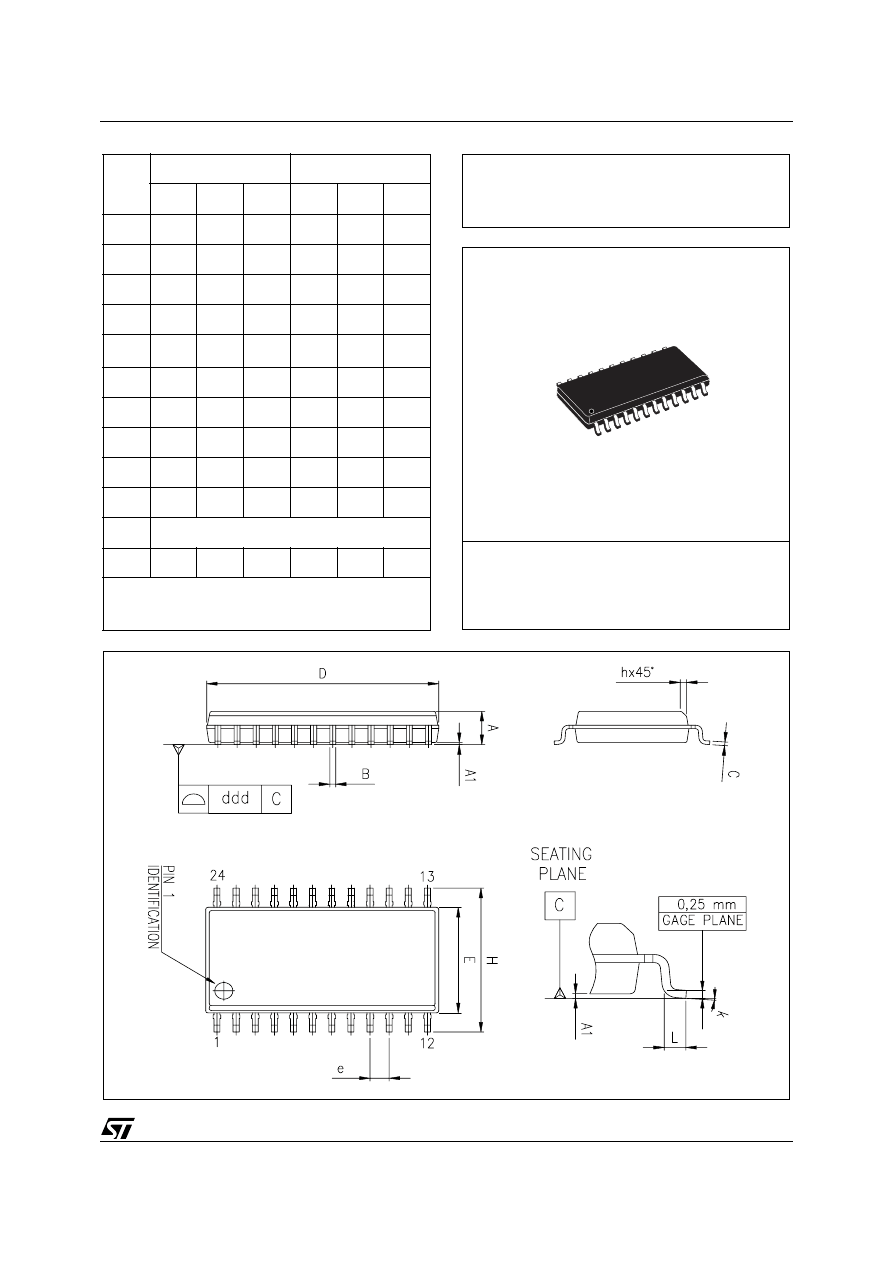
OUTLINE AND
MECHANICAL DATA
DIM.
mm
inch
MIN.
TYP.
MAX.
MIN.
TYP.
MAX.
A
2.35
2.65
0.093
0.104
A1
0.10
0.30
0.004
0.012
B
0.33
0.51
0.013
0.200
C
0.23
0.32
0.009
0.013
D
(1)
15.20
15.60
0.598
0.614
E
7.40
7.60
0.291
0.299
e
1.27
0.050
H
10.0
10.65
0.394
0.419
h
0.25
0;75
0.010
0.030
L
0.40
1.27
0.016
0.050
k
0˚ (min.), 8˚ (max.)
ddd
0.10
0.004
(1) “D” dimension does not include mold flash, protusions or gate
burrs. Mold flash, protusions or gate burrs shall not exceed
0.15mm per side.
SO24
0070769 C
Weight: 0.60gr

Information furnished is believed to be accurate and reliable. However, STMicroelectronics assumes no responsibility for the consequences
of use of such information nor for any infringement of patents or other rights of third parties which may result from its use. No license is granted
by implication or otherwise under any patent or patent rights of STMicroelectronics. Specifications mentioned in this publication are subject
to change without notice. This publication supersedes and replaces all information previously supplied. STMicroelectronics products are not
authorized for use as critical components in life support devices or systems without express written approval of STMicroelectronics.
The ST logo is a registered trademark of STMicroelectronics
2002 STMicroelectronics - All Rights Reserved
STMicroelectronics GROUP OF COMPANIES
Australia - Brazil - Canada - China - Finland - France - Germany - Hong Kong - India - Israel - Italy - Japan -Malaysia - Malta - Morocco -
Singapore - Spain - Sweden - Switzerland - United Kingdom - United States.
http://www.st.com
6/6
LIS2L02AS
Wyszukiwarka
Podobne podstrony:
DIGITAL OUTPUT ANGULAR ACCELEROMETER 8556
Phase Linear 200 II
LinearAlgebra 1(14s) Nieznany
Linear Technology Top Markings Nieznany
linearność i symultaniczność w PJM, migany i migowy
Linear Motor Powered Transportation History, Present Status and Future Outlook
sposoby linearyzacji sygnałów z czujników współpracujących z kondycjonerami
18 Kreteński linearny B
DSaA W02and03 Linear Structures
230 Przykłady notatek linearnych IV
accelerometer f c id 50630 Nieznany (2)
A 20th century acceleration in Nieznany (2)
accelerando
LinearAlgebra 3(5s)
Phase Linear 300
4 Wire EDM V20 2axis from linearc
podst, rekreacji i turystyki oraz linearne syst penetracji rekreacyjnej
więcej podobnych podstron