Description
The GM7800 series are classic regulators, which are use-
ful in a wide range of applications. For example, you can
use them for local on-card regulation to eliminate the distri-
bution and problems associated with single point regula-
tion.
The wide range of output voltages (5V to 27V) make them
useful in an endless list of applications. Although designed
as fixed voltage regulators, you can add a few external
components to make adjustable voltages and currents.
Current limiting prevents the peak output current to a safe
value. Safe-area protection of the output transistor limits in-
ternal power dissipation. If internal power dissipation be-
comes too high for the heat sinking provided, the thermal
shutdown circuit activates to prevent the regulator from
overheating. These versatile workhorses are easy to use.
You do not need to bypass the output, although this does
improve transient response. Input bypass is needed only if
you place the regulator far from the filter capacitor of the
power supply.
The GM7800 series is available in TO-220, TO-252 and
TO-263 packages.
Features
Output current up to 1.5A
Output Voltages 5V, 6V, 8V, 8.5V, 9V, 10V,
12V, 15V, 18V, 20V, 24V and 27V
3- Terminal Regulators
Internal Thermal Overload Protection
Internal Short-Circuit Current Limiting
Output Transistor Safe-Area Protection
TO-220, TO-252 and TO-263 Packages
High Power Dissipation Capability
Direct replacements for LM78xx
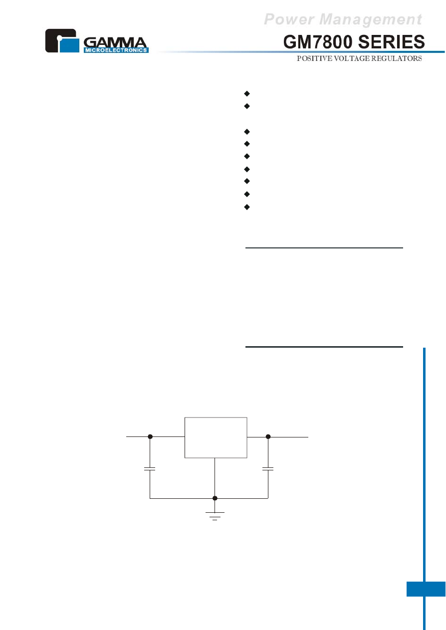
TYPIC APPLICATION CIRCUITS
G
M
7
8
0
0
S
E
R
IE
S
V
0
.1
www.gammamicro.com
1
Application
Post-Regulator Switching DC/DC
Converters
Bias Supply for Analog Circuits
Instrumentation and Audio Systems
Logic Systems
Others too numerous to mention
GM7800
V
IN
V
OUT
0.1µF
0.33µF
GND
1.5A
For a positive regulator, a 0.33µF bypass capacitor should be used on the input terminals.
While not necessary for stability, an output capacitor of 0.1µF may be used to improve the
transient response of the regulator. These capacitors should be on or as near as possible
to the regulator terminals .
V V =Output Voltage(05: 5.0V, 12: 12V)
A =Assembly Location
Y =Year
W W =Weekly
Package
Pro Number
TO-263, TO-220, TO-252
TO-263, TO-220, TO-252
TO-263, TO-220, TO-252
TO-263, TO-220, TO-252
TO-263, TO-220, TO-252
TO-263, TO-220, TO-252
TO-263, TO-220, TO-252
TO-263, TO-220, TO-252
TO-263, TO-220, TO-252
TO-263, TO-220, TO-252
TO-263, TO-220, TO-252
TO-263, TO-220, TO-252
GM7805
GM7806
GM7808
GM7885
GM7809
GM7810
GM7812
GM7815
GM7818
GM7820
GM7824
GM7827
G
M
7
8
0
0
S
E
R
IE
S
2
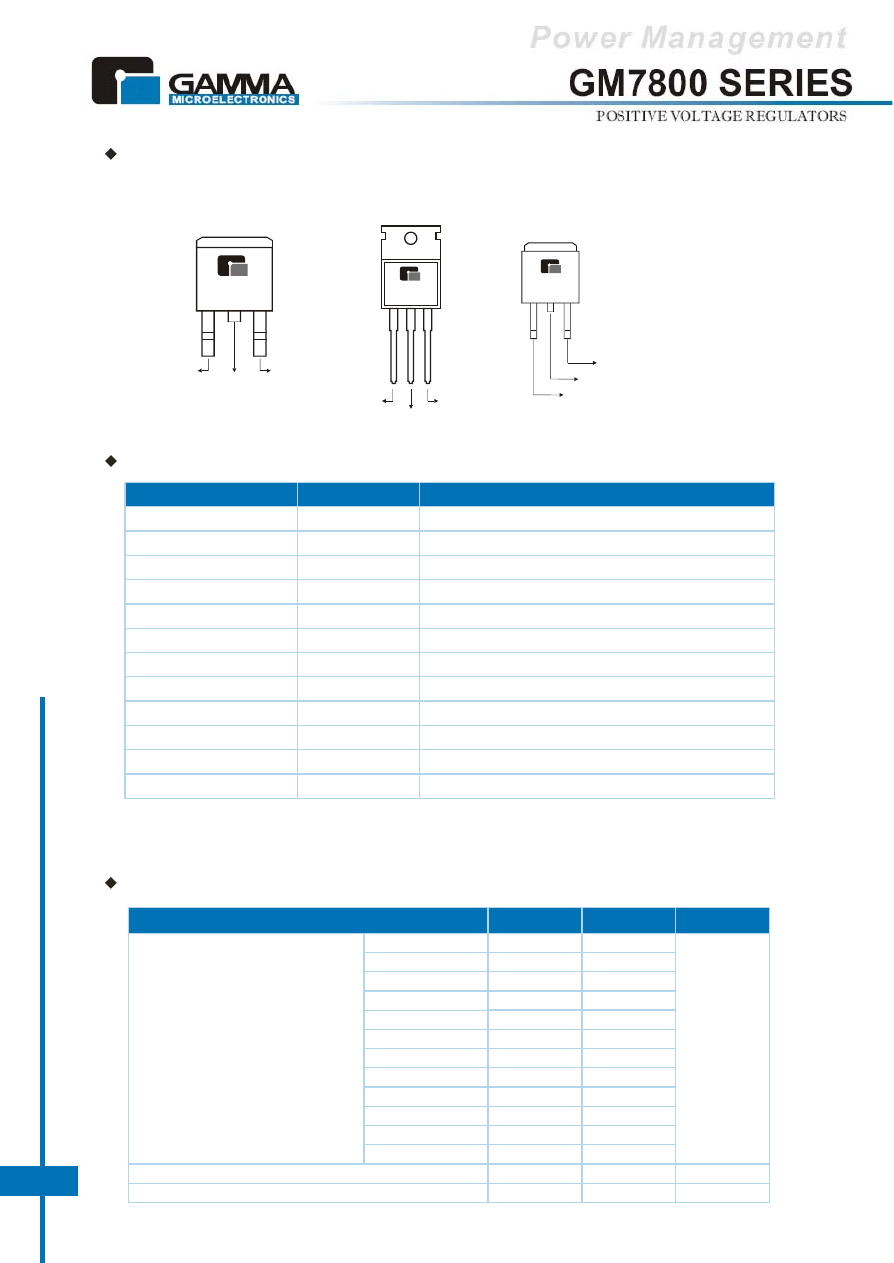
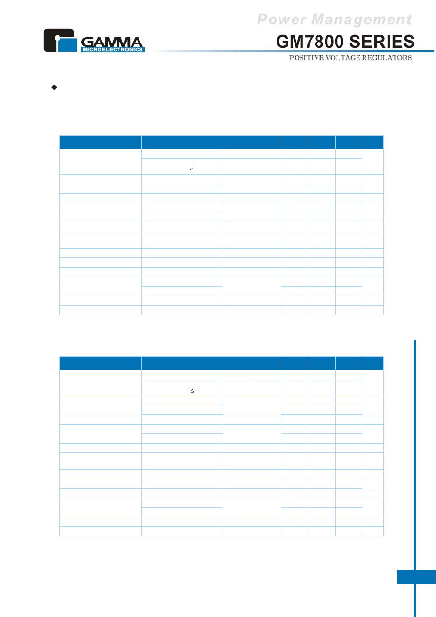
MARKING INFORMATION & PIN CONFIGURATIONS
(TOP VIEW)
ORDERING INFORMATION
GM78VV
AYWW
2
TO-263-2 (D PAK)
INPUT
GND
OUTPUT
TO-220
GM78VV
AYWW
TO-252-3 (DPAK)
GM78VV
AYWW
INPUT
GND
OUTPUT
V
OUT
TAB is GND
V
IN
* For detail Ordering Number identification, please see last page.
V
OUT
5.0V
6.0V
8.0V
8.5V
9.0V
10V
12V
15V
18V
20V
24V
27V
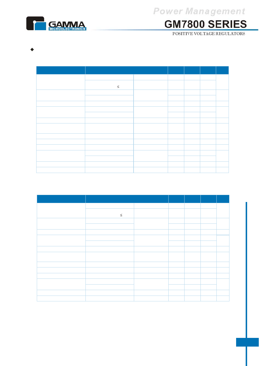
RECOMMENDED OPERATING CONDITIONS (I = 1.5A)
O
PARAMETER
MIN
MAX
UNIT
Input Voltage V
I
GM7805
GM7806
GM7808
GM7885
GM7809
GM7810
GM7812
GM7815
GM7818
GM7820
GM7824
GM7827
Output Current, I
O
Operating virtual junction temperature, T
J
7
8
10.5
10.5
11.5
12.5
14.5
17.5
21
23
27
30
0
25
25
25
25
27
28
30
30
33
36
38
40
1.5
125
V
A
°C
G
M
7
8
0
0
S
E
R
IE
S
3
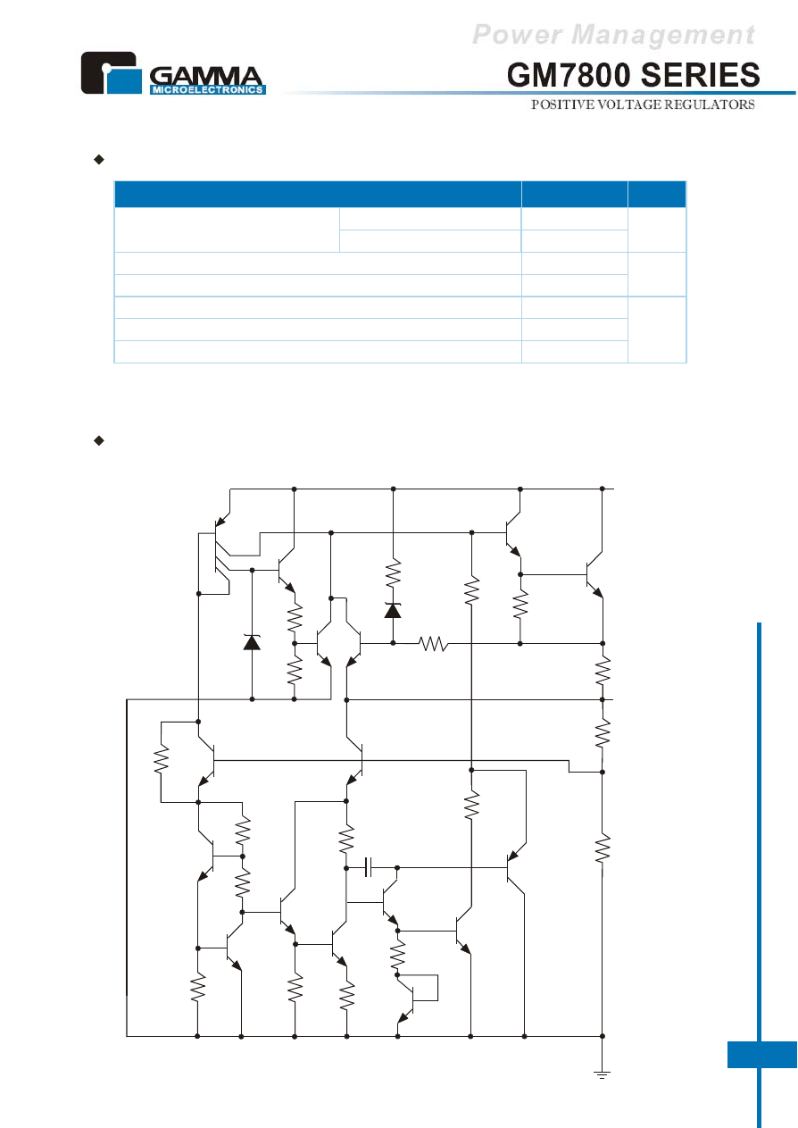
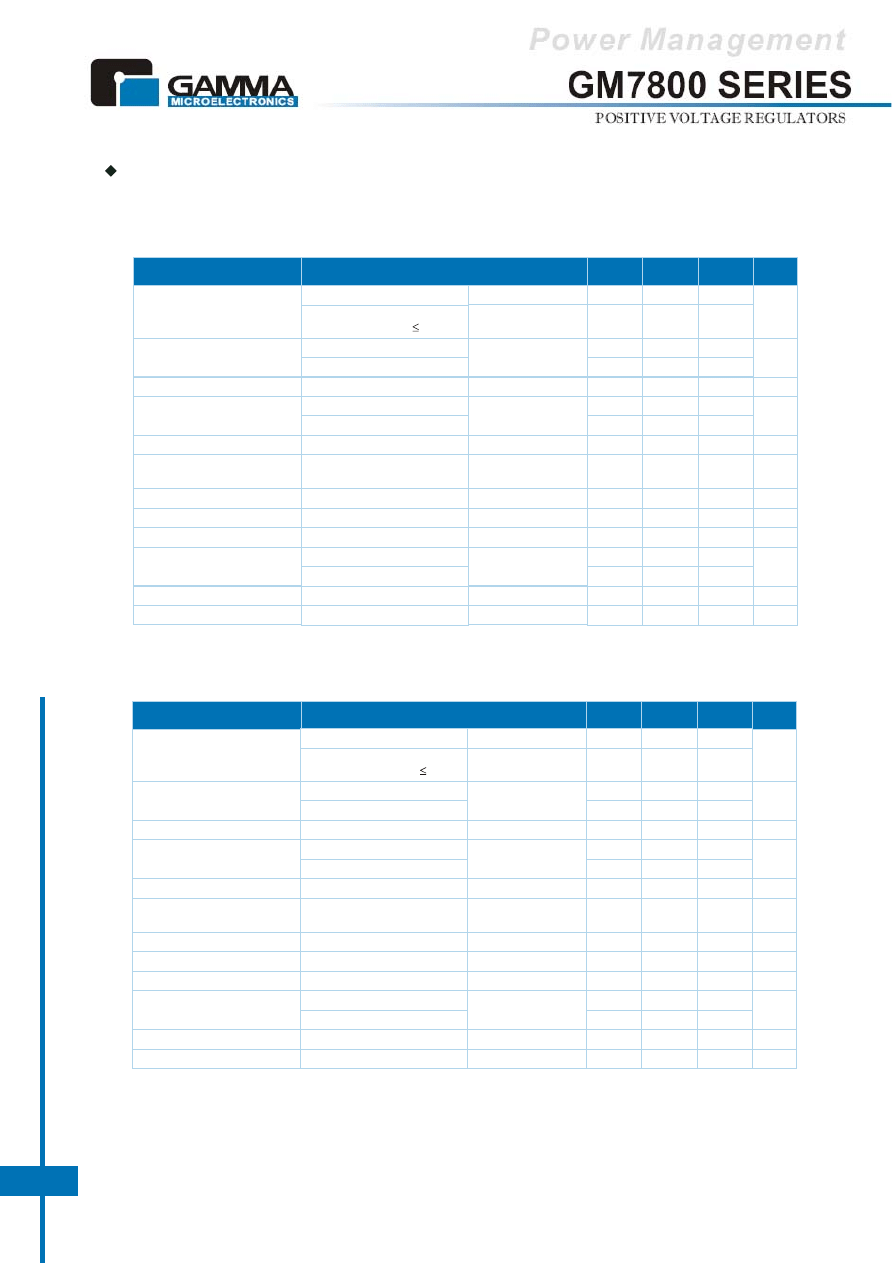
SCHEMATIC BLOCK DIAGRAM
GND
R18
2.6k
R9
4k
R17
R16
0.3k
R15
2k
R10
1k
R13
10k
R1
30k
R4
1.2k
R3
26
R2
1.9k
Q10
OUTPUT
V
REF
Q16
Q15
INPUT
D2
R14
230
R12
200
D1
6.3V
Q11
Q12
Q13
Q14
Q1
Q2
Q3
Q4
Q5
Q9
Q7
Q8
Q6
C1
20pF
R7
17k
R6
1k
R8
4k
R5
12.1k
ABSOLUTE MAXIMUM RATINGS
PARAMETER
VALUE
UNIT
Input Voltage
Continuous Total Dissipation at 25°C free-air temperature
Continuous Total Dissipation at (or bellow) 25°C case Temperature
Operating free-air, case, or virtual junctions Temperature Range
Storage Temperature Range
Lead Temperature 1.6mm (1/16 inch) from case for 10seconds
40
2
15
-65 to +150
260
V
W
0 to +150
°C
GM7824, GM7827
All others
35
G
M
7
8
0
0
S
E
R
IE
S
4
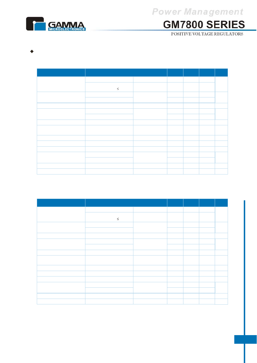
ELECTRICAL CHARACTERISTICS at specified Junction Temperature
GM7805: V = 10V, I = 500mA, (unless otherwise noted)
I
O
CHARACTERISTICS
TEST CONDITIONS *
MIN
TYP
MAX
UNIT
Output Voltage **
4.8
5.0
3
15
78
0.017
750
2.2
-1.1
5.2
100
100
1.3
4.75
5.0
1
5
5.25
50
50
0.5
I = 5mA to 1A
O
V =7V to 20V, P 15W
I
V =7V to 25V
I
I =5mA to 1.5A
O
V = 7V to 25V
I
V =8V to 18V, f = 120Hz
I
f = 1kHz
I = 5mA
O
25°C
25°C
25°C
0°C to 125°C
V
mV
mV
mA
dB
W
Input Regulation
Output Regulation
Bias Current Change
V =8V to 12V
I
I =250mA to 750mA
O
I =5mA to 1A
O
Ripple Rejection
Output Resistance
Short-Circuit Output Current
Peak Output Current
Temperature Coefficient
Output Voltage
0°C to 125°C
0°C to 125°C
25°C
25°C
0°C to 125°C
62
mV/°C
40
2.0
4.2
f = 10Hz to 100kHz
µV
V
mA
Output Noise Voltage
Dropout Voltage
Bias Current
25°C
25°C
25°C
I = 1A
O
8
0°C to 125°C
mA
A
*Pulse testing tehniques are used to maintain the junction temperature as close to the ambient temperature as possible.
Thermal effects must be taken into account.
** The specification applies only for DC power dissipation permitted by absolute maximum ratings
GM7806: V = 11V, I = 500mA, (unless otherwise noted)
I
O
CHARACTERISTICS
TEST CONDITIONS *
MIN
TYP
MAX
UNIT
Output Voltage **
5.75
6
5
14
75
0.019
550
2.2
-0.8
6.25
120
120
1.3
5.7
6
1.5
4
6.3
60
60
0.5
I = 5mA to 1A
O
V =8V to 21V, P 15W
I
V =8V to 25V
I
I =5mA to 1.5A
O
V = 8V to 25V
I
V =9V to 19V, f = 120Hz
I
f = 1kHz
I = 5mA
O
25°C
25°C
25°C
0°C to 125°C
V
mV
mV
mA
dB
W
Input Regulation
Output Regulation
Bias Current Change
V =9V to 13V
I
I =250mA to 750mA
O
I =5mA to 1A
O
Ripple Rejection
Output Resistance
Short-Circuit Output Current
Peak Output Current
Temperature Coefficient
Output Voltage
0°C to 125°C
0°C to 125°C
25°C
25°C
0°C to 125°C
59
mV/°C
45
2.0
4.3
f = 10Hz to 100kHz
µV
V
mA
Output Noise Voltage
Dropout Voltage
Bias Current
25°C
25°C
25°C
I = 1A
O
8
0°C to 125°C
mA
A
G
M
7
8
0
0
S
E
R
IE
S
5
ELECTRICAL CHARACTERISTICS at specified Junction Temperature
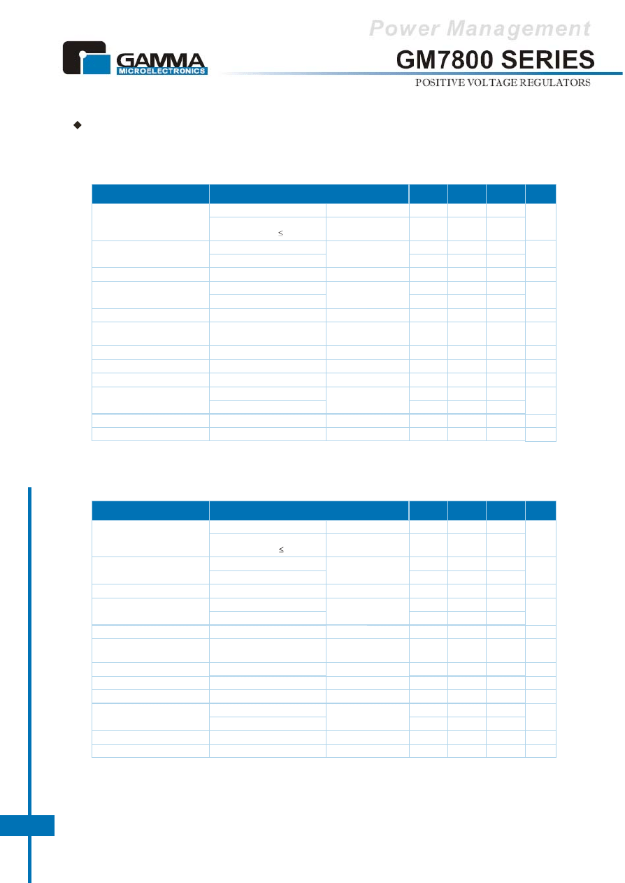
GM7808: V =14V, I =500mA, (unless otherwise noted)
I
O
CHARACTERISTICS
TEST CONDITIONS *
MIN
TYP
MAX
UNIT
Output Voltage **
7.7
8
6
12
72
0.016
450
2.2
-0.8
8.3
160
160
1.0
7.6
8
2
4
8.4
80
80
0.5
I = 5mA to 1A
O
V =10.5V to 23V, P 15W
I
V =10.5V to 25V
I
I =5mA to 1.5A
O
V = 10.5V to 25V
I
V =11.5V to 21.5V, f = 120Hz
I
f = 1kHz
I = 5mA
O
25°C
25°C
25°C
0°C to 125°C
V
mV
mV
mA
dB
W
Input Regulation
Output Regulation
Bias Current Change
V =11V to 17V
I
I =250mA to 750mA
O
I =5mA to 1A
O
Ripple Rejection
Output Resistance
Short-Circuit Output Current
Peak Output Current
Temperature Coefficient
Output Voltage
0°C to 125°C
0°C to 125°C
25°C
25°C
0°C to 125°C
55
mV/°C
52
2.0
4.3
f = 10Hz to 100kHz
µV
V
mA
Output Noise Voltage
Dropout Voltage
Bias Current
25°C
25°C
25°C
I = 1A
O
8
0°C to 125°C
mA
A
*Pulse testing tehniques are used to maintain the junction temperature as close to the ambient temperature as possible.
Thermal effects must be taken into account.
** The specification applies only for DC power dissipation permitted by absolute maximum ratings
GM7885: V =15V, I =500mA, (unless otherwise noted)
I
O
CHARACTERISTICS
TEST CONDITIONS *
MIN
TYP
MAX
UNIT
Output Voltage **
8.15
8.5
6
12
70
0.016
450
2.2
-0.8
8.85
170
170
1.0
8.1
8.5
2
4
8.9
85
85
0.5
I = 5mA to 1A
O
V =11.5V to 23.5V, P 15W
I
V =10.5V to 25V
I
I =5mA to 1.5A
O
V = 10.5V to 25V
I
V =11.5V to 21.5V, f = 120Hz
I
f = 1kHz
I = 5mA
O
25°C
25°C
25°C
0°C to 125°C
V
mV
mV
mA
dB
W
Input Regulation
Output Regulation
Bias Current Change
V =11V to 17V
I
I =250mA to 750mA
O
I =5mA to 1A
O
Ripple Rejection
Output Resistance
Short-Circuit Output Current
Peak Output Current
Temperature Coefficient
Output Voltage
0°C to 125°C
0°C to 125°C
25°C
25°C
0°C to 125°C
54
mV/°C
55
2.0
4.3
f = 10Hz to 100kHz
µV
V
mA
Output Noise Voltage
Dropout Voltage
Bias Current
25°C
25°C
25°C
I = 1A
O
8
0°C to 125°C
mA
A
G
M
7
8
0
0
S
E
R
IE
S
6
*Pulse testing tehniques are used to maintain the junction temperature as close to the ambient temperature as possible.
Thermal effects must be taken into account.
** The specification applies only for DC power dissipation permitted by absolute maximum ratings
GM7809: V =16V, I =500mA, (unless otherwise noted)
I
O
CHARACTERISTICS
TEST CONDITIONS *
MIN
TYP
MAX
UNIT
Output Voltage **
8.65
9
7
12
70
0.018
400
2.2
-1.0
9.35
180
180
1.0
8.55
9
2
4
9.45
90
90
0.5
I = 5mA to 1A
O
V =11.5V to 24V, P 15W
I
V =11.5V to 27V
I
I =5mA to 1.5A
O
V = 11.5V to 27V
I
V =12V to 22V, f = 120Hz
I
f = 1kHz
I = 5mA
O
25°C
25°C
25°C
0°C to 125°C
V
mV
mV
mA
dB
W
Input Regulation
Output Regulation
Bias Current Change
V =13V to 19V
I
I =250mA to 750mA
O
I =5mA to 1A
O
Ripple Rejection
Output Resistance
Short-Circuit Output Current
Peak Output Current
Temperature Coefficient
Output Voltage
0°C to 125°C
0°C to 125°C
25°C
25°C
0°C to 125°C
55
mV/°C
60
2.0
4.3
f = 10Hz to 100kHz
µV
V
mA
Output Noise Voltage
Dropout Voltage
Bias Current
25°C
25°C
25°C
I = 1A
O
8
0°C to 125°C
mA
A
ELECTRICAL CHARACTERISTICS at specified Junction Temperature
GM7810: V = 17V, I = 500mA, (unless otherwise noted)
I
O
CHARACTERISTICS
TEST CONDITIONS *
MIN
TYP
MAX
UNIT
Output Voltage **
9.6
10
7
12
71
0.018
400
2.2
-1.0
10.4
200
200
1.0
9.5
10
2
4
10.5
100
100
0.5
I = 5mA to 1A
O
V =12.5V to 25V, P 15W
I
V =12.5V to 28V
I
I =5mA to 1.5A
O
V = 12.5V to 28V
I
V =13V to 23V, f = 120Hz
I
f = 1kHz
I = 5mA
O
25°C
25°C
25°C
0°C to 125°C
V
mV
mV
mA
dB
W
Input Regulation
Output Regulation
Bias Current Change
V =14V to 20V
I
I =250mA to 750mA
O
I =5mA to 1A
O
Ripple Rejection
Output Resistance
Short-Circuit Output Current
Peak Output Current
Temperature Coefficient
Output Voltage
0°C to 125°C
0°C to 125°C
25°C
25°C
0°C to 125°C
55
mV/°C
70
2.0
4.3
f = 10Hz to 100kHz
µV
V
mA
Output Noise Voltage
Dropout Voltage
Bias Current
25°C
25°C
25°C
I = 1A
O
8
0°C to 125°C
mA
A
G
M
7
8
0
0
S
E
R
IE
S
7
ELECTRICAL CHARACTERISTICS at specified Junction Temperature
GM7812: V =19V, I =500mA, (unless otherwise noted)
I
O
CHARACTERISTICS
TEST CONDITIONS *
MIN
TYP
MAX
UNIT
Output Voltage **
11.5
12
10
12
71
0.018
350
2.2
-1.0
12.5
240
240
1.0
11.4
12
3
4
12.6
120
120
0.5
I = 5mA to 1A
O
V =14.5V to 27V, P 15W
I
V =14.5V to 30V
I
I =5mA to 1.5A
O
V = 14.5V to 30V
I
V =15V to 25V, f = 120Hz
I
f = 1kHz
I = 5mA
O
25°C
25°C
25°C
0°C to 125°C
V
mV
mV
mA
dB
W
Input Regulation
Output Regulation
Bias Current Change
V =16V to 22V
I
I =250mA to 750mA
O
I =5mA to 1A
O
Ripple Rejection
Output Resistance
Short-Circuit Output Current
Peak Output Current
Temperature Coefficient
Output Voltage
0°C to 125°C
0°C to 125°C
25°C
25°C
0°C to 125°C
55
mV/°C
75
2.0
4.3
f = 10Hz to 100kHz
µV
V
mA
Output Noise Voltage
Dropout Voltage
Bias Current
25°C
25°C
25°C
I = 1A
O
8
0°C to 125°C
mA
A
*Pulse testing tehniques are used to maintain the junction temperature as close to the ambient temperature as possible.
Thermal effects must be taken into account.
** The specification applies only for DC power dissipation permitted by absolute maximum ratings
GM7815: V =23V, I =500mA, (unless otherwise noted)
I
O
CHARACTERISTICS
TEST CONDITIONS *
MIN
TYP
MAX
UNIT
Output Voltage **
14.4
15
12
12
70
0.019
230
2.1
-1.0
15.6
300
300
1.0
14.25
15
3
4
15.75
150
150
0.5
I = 5mA to 1A
O
V =17.5V to 30V, P 15W
I
V =17.5V to 30V
I
I =5mA to 1.5A
O
V = 17.5V to 30V
I
V =18.5V to 28.5V, f = 120Hz
I
f = 1kHz
I = 5mA
O
25°C
25°C
25°C
0°C to 125°C
V
mV
mV
mA
dB
W
Input Regulation
Output Regulation
Bias Current Change
V =20V to 26V
I
I =250mA to 750mA
O
I =5mA to 1A
O
Ripple Rejection
Output Resistance
Short-Circuit Output Current
Peak Output Current
Temperature Coefficient
Output Voltage
0°C to 125°C
0°C to 125°C
25°C
25°C
0°C to 125°C
54
mV/°C
90
2.0
4.3
f = 10Hz to 100kHz
µV
V
mA
Output Noise Voltage
Dropout Voltage
Bias Current
25°C
25°C
25°C
I = 1A
O
8
0°C to 125°C
mA
A
G
M
7
8
0
0
S
E
R
IE
S
8
ELECTRICAL CHARACTERISTICS at specified Junction Temperature
GM7818: V =27V, I =500mA, (unless otherwise noted)
I
O
CHARACTERISTICS
TEST CONDITIONS *
MIN
TYP
MAX
UNIT
Output Voltage **
17.3
18
15
12
69
0.022
200
2.1
-1.0
18.7
360
360
1.0
17.1
18
5
4
18.9
180
180
0.5
I = 5mA to 1A
O
V =21V to 33V, P 15W
I
V =21V to 33V
I
I =5mA to 1.5A
O
V = 21V to 33V
I
V =22V to 32V, f = 120Hz
I
f = 1kHz
I = 5mA
O
25°C
25°C
25°C
0°C to 125°C
V
mV
mV
mA
dB
W
Input Regulation
Output Regulation
Bias Current Change
V =24V to 30V
I
I =250mA to 750mA
O
I =5mA to 1A
O
Ripple Rejection
Output Resistance
Short-Circuit Output Current
Peak Output Current
Temperature Coefficient
Output Voltage
0°C to 125°C
0°C to 125°C
25°C
25°C
0°C to 125°C
53
mV/°C
110
2.0
4.5
f = 10Hz to 100kHz
µV
V
mA
Output Noise Voltage
Dropout Voltage
Bias Current
25°C
25°C
25°C
I = 1A
O
8
0°C to 125°C
mA
A
*Pulse testing tehniques are used to maintain the junction temperature as close to the ambient temperature as possible.
Thermal effects must be taken into account.
** The specification applies only for DC power dissipation permitted by absolute maximum ratings
GM7820: V =29V, I =500mA, (unless otherwise noted)
I
O
CHARACTERISTICS
TEST CONDITIONS *
MIN
TYP
MAX
UNIT
Output Voltage **
19.2
20
18
15
66
0.027
180
2.1
-1.3
20.8
400
400
1.0
19
20
7
7
21
200
200
0.5
I = 5mA to 1A
O
V =23V to 35V, P 15W
I
V =23V to 35V
I
I =5mA to 1.5A
O
V = 23V to 35V
I
V =24V to 34V, f = 120Hz
I
f = 1kHz
I = 5mA
O
25°C
25°C
25°C
0°C to 125°C
V
mV
mV
mA
dB
W
Input Regulation
Output Regulation
Bias Current Change
V =26V to 32V
I
I =250mA to 750mA
O
I =5mA to 1A
O
Ripple Rejection
Output Resistance
Short-Circuit Output Current
Peak Output Current
Temperature Coefficient
Output Voltage
0°C to 125°C
0°C to 125°C
25°C
25°C
0°C to 125°C
51
mV/°C
150
2.0
4.5
f = 10Hz to 100kHz
µV
V
mA
Output Noise Voltage
Dropout Voltage
Bias Current
25°C
25°C
25°C
I = 1A
O
8
0°C to 125°C
mA
A
ELECTRICAL CHARACTERISTICS at specified Junction Temperature
GM7824: V =33V, I =500mA, (unless otherwise noted)
I
O
CHARACTERISTICS
TEST CONDITIONS *
MIN
TYP
MAX
UNIT
Output Voltage **
23
24
18
12
66
0.028
150
2.1
-1.5
25
480
480
1.0
22.8
24
6
4
25.2
240
240
0.5
I = 5mA to 1A
O
V =27V to 38V, P 15W
I
V =27V to 38V
I
I =5mA to 1.5A
O
V = 27V to 38V
I
V =28V to 32V, f = 120Hz
I
f = 1kHz
I = 5mA
O
25°C
25°C
25°C
0°C to 125°C
V
mV
mV
mA
dB
W
Input Regulation
Output Regulation
Bias Current Change
V =30V to 36V
I
I =250mA to 750mA
O
I =5mA to 1A
O
Ripple Rejection
Output Resistance
Short-Circuit Output Current
Peak Output Current
Temperature Coefficient
Output Voltage
0°C to 125°C
0°C to 125°C
25°C
25°C
0°C to 125°C
50
mV/°C
170
2.0
4.6
f = 10Hz to 100kHz
µV
V
mA
Output Noise Voltage
Dropout Voltage
Bias Current
25°C
25°C
25°C
I = 1A
O
8
0°C to 125°C
mA
A
*Pulse testing tehniques are used to maintain the junction temperature as close to the ambient temperature as possible.
Thermal effects must be taken into account.
** The specification applies only for DC power dissipation permitted by absolute maximum ratings
GM7827: V =36V, I =500mA, (unless otherwise noted)
I
O
CHARACTERISTICS
TEST CONDITIONS *
MIN
TYP
MAX
UNIT
Output Voltage **
25.9
27
25
20
64
0.030
120
2.1
-1.6
28.1
540
540
1.0
25.7
27
10
9
28.3
270
270
0.5
I = 5mA to 1A
O
V =30V to 40V, P 15W
I
V =30V to 40V
I
I =5mA to 1.5A
O
V = 30V to 40V
I
V =30V to 40V, f = 120Hz
I
f = 1kHz
I = 5mA
O
25°C
25°C
25°C
0°C to 125°C
V
mV
mV
mA
dB
W
Input Regulation
Output Regulation
Bias Current Change
V =33V to 39V
I
I =250mA to 750mA
O
I =5mA to 1A
O
Ripple Rejection
Output Resistance
Short-Circuit Output Current
Peak Output Current
Temperature Coefficient
Output Voltage
0°C to 125°C
0°C to 125°C
25°C
25°C
0°C to 125°C
50
mV/°C
200
2.0
4.8
f = 10Hz to 100kHz
µV
V
mA
Output Noise Voltage
Dropout Voltage
Bias Current
25°C
25°C
25°C
I = 1A
O
8
0°C to 125°C
mA
A
G
M
7
8
0
0
S
E
R
IE
S
9
G
M
7
8
0
0
S
E
R
IE
S
10
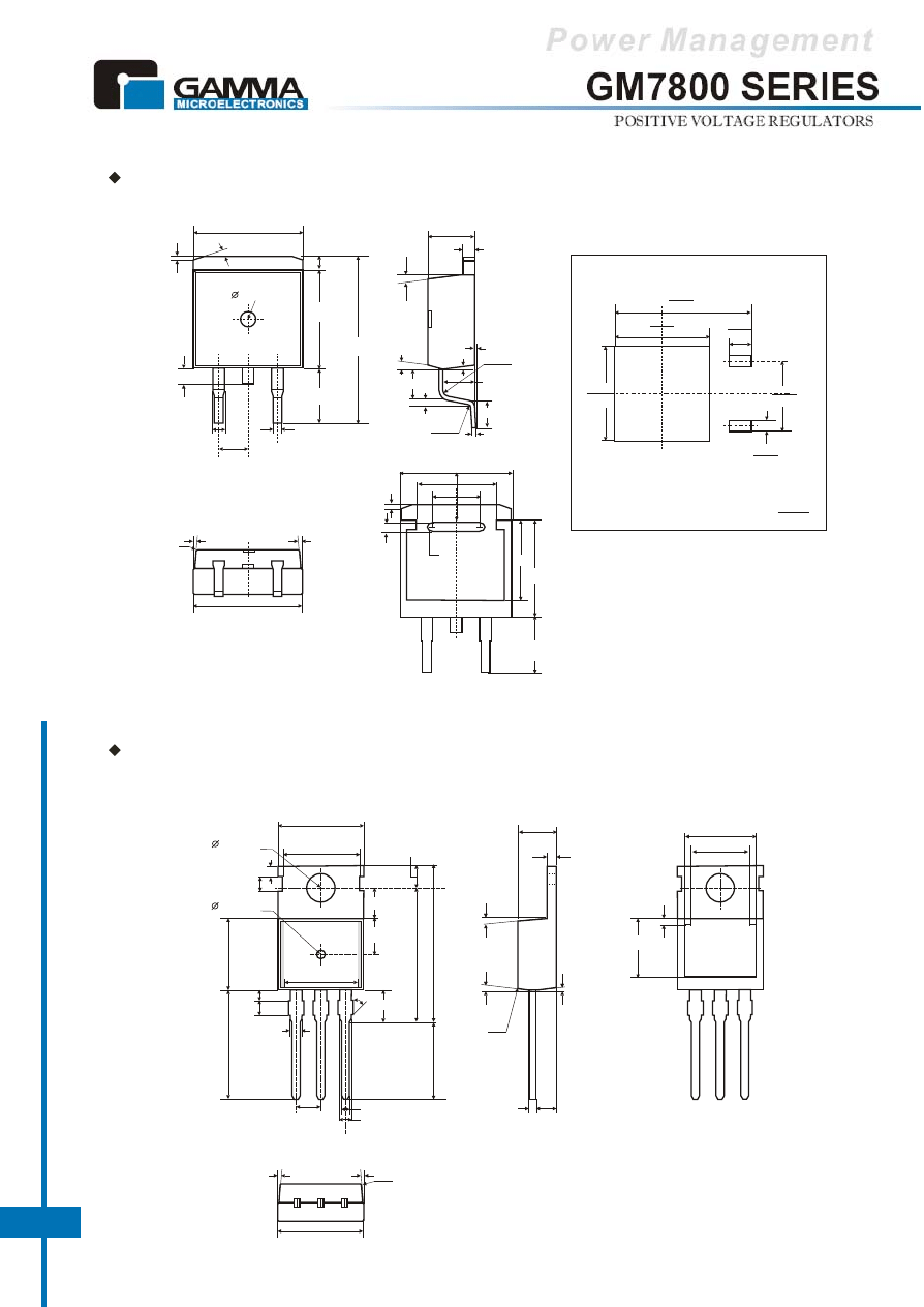
TO-220 PACKAGE OUTLINE DIMENSIONS
TO-263-2 PACKAGE OUTLINE DIMENSIONS
Pad Layout
9.90 ± 0.20
15°
0.40
1.50 DP0.20
9.20 ± 0.20
4.90 ± 0.20
15.3 ± 0.20
1.27 ± 0.10
0.90 ± 0.10
2.54 TYP
(2.54 ± 0.20)
1.4 ± 0.20
3°
4.50 ± 0.20
1.30
+0.1
-0.05
0.10 ± 0.01
2.40 ± 0.20
2.00 ± 0.10
R0.30
R0.30
2.54 ± 0.10
0.50
+0.1
-0.05
4.0
7.0
10.0 ± 0.20
0.40
0.90
7.2
9.20 ± 0.20
4.90 ± 0.20
Unit: mm
10.00 ± 0.20
3°
3°
0.33
8.38
0.63
17.02
0.12
3.05
0.04
1.016
0.24
6.096
0.42
10.66
Inches
mm
( )
1.20
R 0.45
0.75
3°
3°
R 0.3
9.90 ± 0.20
3.60 ± 0.20
1.50 DP0.20
1
3
.0
8
±
0
.2
0
9
.2
0
±
0
.2
0
3.70 ± 0.20
1.30
2.80 ± 0.10
1
5
.9
0
±
0
.2
0
1
8
.9
5
M
A
X
1
0
.0
8
±
0
.3
0
1.52 ± 0.10
0.80 ± 0.10
2.54 TYP
(2.54 ± 0.20)
0.50
2.40 ± 0.20
Unit: mm
1.30 ± 0.10
4.50 ± 0.20
8.70
1.70
4.60
1.46
1.00
3.00
45°
+0.1
-0.05
3°
3°
3°
+0.1
-0.05
8.0
7.0
7.0
0.9
3-R0.2
10.00 ± 0.20
3°
3°
8.40
1.27 ± 0.10
2 - R 0.3
G
M
7
8
0
0
S
E
R
IE
S
11
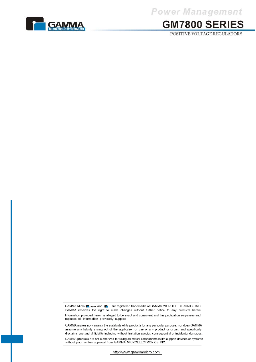
ORDERING NUMBER
GM
78
00 TA3 T
Gamma Micro.
Circuit Type
Package
TA3: TO-263
TB3: TO-220
TC3: TO-252
50 Units/ Tube
800 Units/ Tape & Reel
80 Units/ Tube
80 Units/ Tube
2,500 Units/ Tape & Reel
Shipping
R: Tape & Reel
T: Tube
Output Voltage
05: 5.0V, 06: 6.0V
08: 8.0V, 8.5:8.5V
09: 9.0V, 10:10V
12: 12V, 15: 15V
18: 18V, 20: 20V
24: 24V, 27: 27V
TO-252 PACKAGE OUTLINE DIMENSIONS
6.50 ± 0.05
5.340 ± 0.05
29° ± 0.5°
REF 0.6
6.10 ± 0.05
7.20 ± 0.05
0.75 ± 0.10
0.89 ± 0.05
0.81 ± 0.038
2.30 ± 0.05
0.508 ± 0.0127
7°
7°
7°
0.070 ± 0.05
1.0 ± 0.05
0.75 ± 0.10
1.525 ± 0.10
2.70 ± 0.10
9.900
2°
R0.15 max
Unit: mm
R 0.25 ± 0.13
Pad Layout
0.244
6.20
0.228
5.80
0.118
3.0
0.063
1.6
0.243
6.172
0.101
2.58
Inches
mm
( )
G
M
7
8
0
0
S
E
R
IE
S
12
Document Outline
Wyszukiwarka
Podobne podstrony:
A11VLO250 Series 10
CITROEN XM SERIES I&II DIAGNOZA KODY MIGOWE INSTRUKCJA
A10VO Series 31 Size 28 Service Parts list
Hitachi Vm Series Camcorder Servicing
02 Ashtanga Yoga Series1
18 Series Tandem Pump Exploded View
Bushings DF 2200 SERIES
Chandin Whitten Beautiful Misery (Beautiful Series #2)
Eaton Series 1 Model 33 64 Variable Pump Parts
Mathematics HL November 2008P3 Series
Woolf The Common Reader Second Series
Akumulator do HYSTER00 series sweeper BriggsStratton England
Focus S Series Hand Held and GUI Instrukcja Obsługi
18 Series Variable Pump Exploded View
AA4VG Series 32 Size 40 Service Parts List
Jvc Hr J64X Series Fault Codes
więcej podobnych podstron