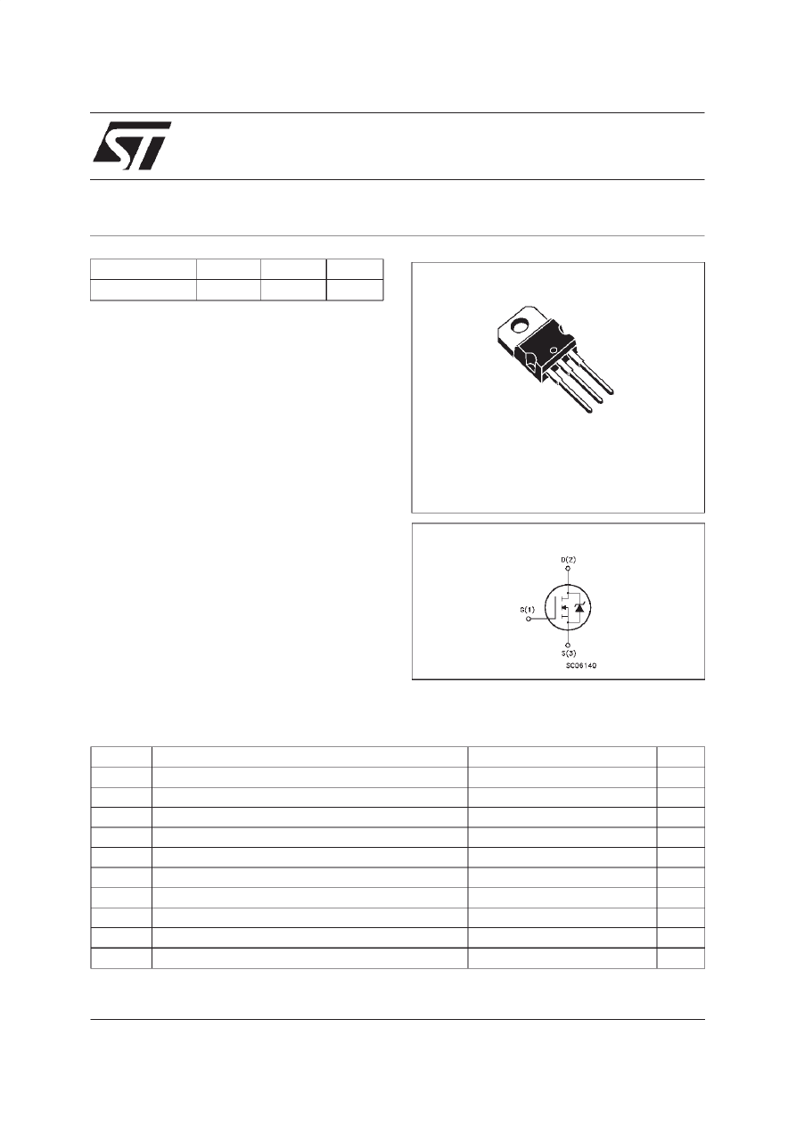
BUZ71A
N - CHANNEL 50V - 0.1
Ω
- 13A -TO-220
STripFET
POWER MOSFET
■
TYPICAL R
DS(on)
= 0.1
Ω
■
AVALANCHE RUGGED TECHNOLOGY
■
100% AVALANCHE TESTED
■
HIGH CURRENT CAPABILITY
■
175
o
C OPERATING TEMPERATURE
APPLICATIONS
■
HIGH CURRENT, HIGH SPEED SWITCHING
■
SOLENOID AND RELAY DRIVERS
■
REGULATORS
■
DC-DC & DC-AC CONVERTERS
■
MOTOR CONTROL, AUDIO AMPLIFIERS
■
AUTOMOTIVE ENVIRONMENT (INJECTION,
ABS, AIR-BAG, LAMPDRIVERS, Etc.)
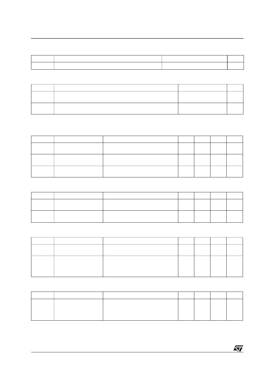
INTERNAL SCHEMATIC DIAGRAM
August 1998
ABSOLUTE MAXIMUM RATINGS
Symbol
Parameter
Value
Uni t
V
DS
Drain-source Volt age (V
GS
= 0)
50
V
V
DGR
Drain- gate Voltage (R
GS
= 20 k
Ω
)
50
V
V
G S
Gat e-source Voltage
±
20
V
I
D
Drain Current (continuous) at T
c
= 25
o
C
13
A
I
DM
Drain Current (pulsed)
52
A
P
t ot
Tot al Dissipation at T
c
= 25
o
C
40
W
T
stg
Storage T emperat ure
-65 to 175
o
C
T
j
Max. O perating Junction Temperature
175
o
C
DIN HUMIDIT Y CAT EGO RY (DI N 40040)
E
IEC CLI MATIC CATEG ORY (DI N I EC 68-1)
55/ 150/56
First digit of the datecode being Z or K identifies silicon characterized in this datasheet.
T YPE
V
DSS
R
DS(o n)
I
D
BUZ71A
50 V
< 0. 12
Ω
13 A
1
2
3
TO-220
1/6
THERMAL DATA
R
t hj-ca se
Thermal Resistance Junction-case
Max
3.1
o
C/W
R
t hj- amb
Thermal Resistance Junction-ambient
Max
62. 5
o
C/W
AVALANCHE CHARACTERISTICS
Symb ol
Parameter
Value
Uni t
I
AR
Avalanche Current, Repetitive or Not -Repet itive
(pulse width limited by T
j
max,
δ
< 1%)
14
A
E
AS
Single Pulse Avalanche Energy
(starting T
j
= 25
o
C, I
D
= I
AR
, V
DD
= 25 V)
50
mJ
ELECTRICAL CHARACTERISTICS (T
case
= 25
o
C unless otherwise specified)
OFF
Symb ol
Parameter
Test Cond ition s
Mi n.
Typ .
Max.
Un it
V
(BR)DSS
Drain-source
Breakdown Volt age
I
D
= 250
µ
A
V
GS
= 0
50
V
I
DSS
Zero G ate Voltage
Drain Current (V
GS
= 0)
V
DS
= Max Rating
V
DS
= Max Rating
T
j
= 125
o
C
1
10
µ
A
µ
A
I
GSS
Gate-body Leakage
Current (V
DS
= 0)
V
G S
=
±
20 V
±
100
nA
ON (
∗
)
Symb ol
Parameter
Test Cond ition s
Mi n.
Typ .
Max.
Un it
V
GS(th)
Gate Threshold
Voltage
V
DS
= V
GS
I
D
= 1 mA
2. 1
3
4
V
R
DS( on)
St atic Drain-source On
Resistance
V
G S
= 10 V
I
D
= 9 A
0.1
0.12
Ω
DYNAMIC
Symb ol
Parameter
Test Cond ition s
Mi n.
Typ .
Max.
Un it
g
fs
(
∗
)
Forward
Transconduct ance
V
DS
= 25 V
I
D
= 9 A
4
7.7
S
C
iss
C
oss
C
rss
Input Capacitance
Output Capacit ance
Reverse T ransfer
Capacitance
V
DS
= 25 V
f = 1 MHz
V
GS
= 0
760
100
30
pF
pF
pF
SWITCHING
Symb ol
Parameter
Test Cond ition s
Mi n.
Typ .
Max.
Un it
t
d(on)
t
r
t
d(of f)
t
f
Turn-on Time
Rise Time
Turn-off Delay Time
Fall Time
V
DD
= 30 V
I
D
= 8 A
R
GS
= 50
Ω
V
GS
= 10 V
20
65
70
35
ns
ns
ns
ns
BUZ71A
2/6
ELECTRICAL CHARACTERISTICS (continued)
SOURCE DRAIN DIODE
Symb ol
Parameter
Test Cond ition s
Mi n.
Typ .
Max.
Un it
I
SD
I
SDM
Source-drain Current
Source-drain Current
(pulsed)
13
52
A
A
V
SD
(
∗
)
Forward On Voltage
I
SD
= 28 A
V
GS
= 0
1.8
V
t
rr
Q
rr
Reverse Recovery
Time
Reverse Recovery
Charge
I
SD
= 14 A
di/dt = 100 A/
µ
s
V
DD
= 30 V
T
j
= 150
o
C
65
0. 17
ns
µ
C
(
∗
) Pulsed: Pulse duration = 300
µ
s, duty cycle 1.5 %
BUZ71A
3/6
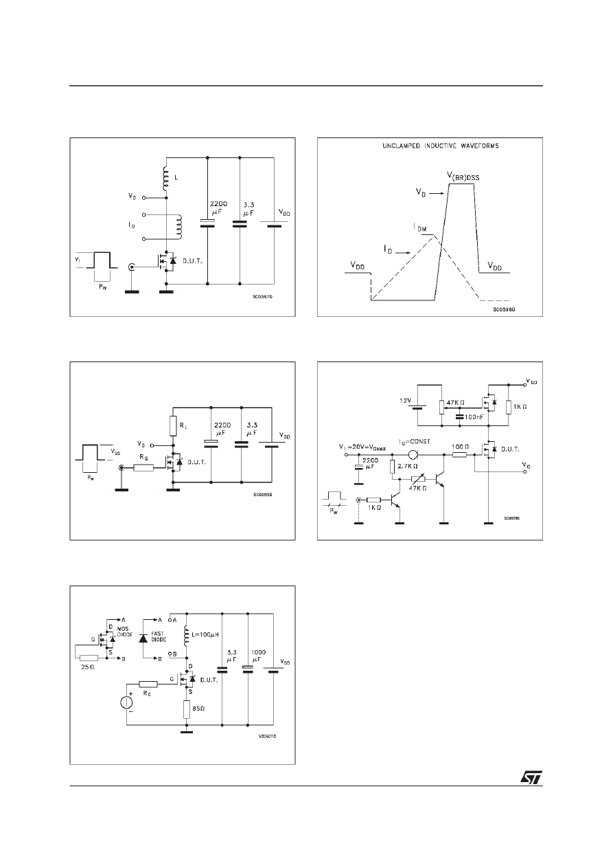
Fig. 1: Unclamped Inductive Load Test Circuit
Fig. 3: Switching Times Test Circuits For
Resistive Load
Fig. 2: Unclamped Inductive Waveform
Fig. 4: Gate Charge test Circuit
Fig. 5: Test Circuit For Inductive Load Switching
And Diode Recovery Times
BUZ71A
4/6
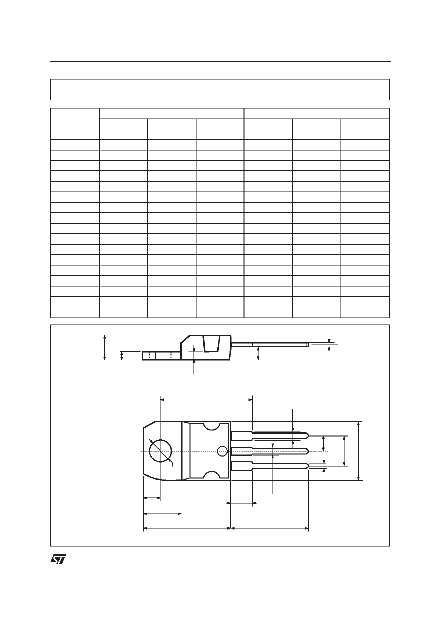
DIM.
mm
inch
MIN.
TYP.
MAX.
MIN.
TYP.
MAX.
A
4.40
4.60
0.173
0.181
C
1.23
1.32
0.048
0.051
D
2.40
2.72
0.094
0.107
D1
1.27
0.050
E
0.49
0.70
0.019
0.027
F
0.61
0.88
0.024
0.034
F1
1.14
1.70
0.044
0.067
F2
1.14
1.70
0.044
0.067
G
4.95
5.15
0.194
0.203
G1
2.4
2.7
0.094
0.106
H2
10.0
10.40
0.393
0.409
L2
16.4
0.645
L4
13.0
14.0
0.511
0.551
L5
2.65
2.95
0.104
0.116
L6
15.25
15.75
0.600
0.620
L7
6.2
6.6
0.244
0.260
L9
3.5
3.93
0.137
0.154
DIA.
3.75
3.85
0.147
0.151
L6
A
C
D
E
D1
F
G
L7
L2
Dia.
F1
L5
L4
H2
L9
F2
G1
TO-220 MECHANICAL DATA
P011C
BUZ71A
5/6

Information furnished is believed to be accurate and reliable. However, STMicroelectronics assumes no responsibility for the consequences
of use of such information nor for any infringement of patents or other rights of third parties which may result from its use. No license is
granted by implication or otherwise under any patent or patent rights of STMicroelectronics. Specification mentioned in this publication are
subject to change without notice. This publication supersedes and replaces all information previously supplied. STMicroelectronics products
are not authorized for use as critical components in life support devices or systems without express written approval of STMicroelectronics.
The ST logo is a registered trademark of STMicroelectronics
1998 STMicroelectronics – Printed in Italy – All Rights Reserved
STMicroelectronics GROUP OF COMPANIES
Australia - Brazil - Canada - China - France - Germany - Italy - Japan - Korea - Malaysia - Malta - Mexico - Morocco - The Netherlands -
Singapore - Spain - Sweden - Switzerland - Taiwan - Thailand - United Kingdom - U.S.A.
.
BUZ71A
6/6
Wyszukiwarka
Podobne podstrony:
2951
2951
2951
2951
2951
2951
2951
2951
Leigh Michaels Strictly Business [HR 2951, MB 2855] (v0 9) (docx)
Instrukcja Electrolux ERB 2951
2951
więcej podobnych podstron