µ
A741,
µ
A741Y
GENERAL-PURPOSE OPERATIONAL AMPLIFIERS
SLOS094A – NOVEMBER 1970 – REVISED JANUARY 1992
1
POST OFFICE BOX 655303
•
DALLAS, TEXAS 75265
D
Short-Circuit Protection
D
Offset-Voltage Null Capability
D
Large Common-Mode and Differential
Voltage Ranges
D
No Frequency Compensation Required
D
Low Power Consumption
D
No Latch-Up
D
Designed to Be Interchangeable With
Fairchild
µ
A741
description
The
µ
A741 is a general-purpose operational
amplifier featuring offset-voltage null capability.
The high common-mode input voltage range and
the absence of latch-up make the amplifier ideal
for voltage-follower applications. The device is
short-circuit protected and the internal frequency
compensation ensures stability without external
components. A low value potentiometer may be
connected between the offset null inputs to null
out the offset voltage as shown in Figure 2.
The
µ
A741C is characterized for operation from
0
°
C to 70
°
C. The
µ
A741I is characterized for
operation from – 40
°
C to 85
°
C.The
µ
A741M is
characterized for operation over the full military
temperature range of – 55
°
C to 125
°
C.
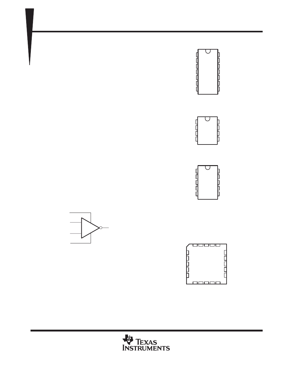
symbol
IN +
IN –
OUT
+
–
OFFSET N1
OFFSET N2
Copyright
1992, Texas Instruments Incorporated
PRODUCTION DATA information is current as of publication date.
Products conform to specifications per the terms of Texas Instruments
standard warranty. Production processing does not necessarily include
testing of all parameters.
1
2
3
4
5
6
7
14
13
12
11
10
9
8
NC
NC
OFFSET N1
IN –
IN +
V
CC
–
NC
NC
NC
NC
V
CC +
OUT
OFFSET N2
NC
µ
A741M . . . J PACKAGE
(TOP VIEW)
1
2
3
4
8
7
6
5
OFFSET N1
IN –
IN +
V
CC –
NC
V
CC+
OUT
OFFSET N2
µ
A741M . . . JG PACKAGE
µ
A741C,
µ
A741I . . . D, P, OR PW PACKAGE
(TOP VIEW)
1
2
3
4
5
10
9
8
7
6
NC
OFFSET N1
IN –
IN +
V
CC –
NC
NC
V
CC +
OUT
OFFSET N2
µ
A741M . . . U PACKAGE
(TOP VIEW)
3
2
1 20 19
9 10 11 12 13
4
5
6
7
8
18
17
16
15
14
NC
V
CC +
NC
OUT
NC
NC
IN –
NC
IN +
NC
µ
A741M . . . FK PACKAGE
(TOP VIEW)
NC
OFFSET
N1
NC
OFFSET
N2
NC
NC
NC
NC
V
NC
CC–
NC – No internal connection
µ
A741,
µ
A741Y
GENERAL-PURPOSE OPERATIONAL AMPLIFIERS
SLOS094A – NOVEMBER 1970 – REVISED JANUARY 1992
2
POST OFFICE BOX 655303
•
DALLAS, TEXAS 75265
AVAILABLE OPTIONS
PACKAGED DEVICES
CHIP
TA
SMALL
OUTLINE
(D)
CHIP
CARRIER
(FK)
CERAMIC
DIP
(J)
CERAMIC
DIP
(JG)
PLASTIC
DIP
(P)
TSSOP
(PW)
FLAT
PACK
(U)
CHIP
FORM
(Y)
0
°
C to 70
°
C
uA741CD
uA741CP
uA741CPW
uA741Y
– 40
°
C to 85
°
C
uA741ID
uA741IP
– 55
°
C to 125
°
C
uA741MFK
uA741MJ
uA741MJG
uA741MU
The D package is available taped and reeled. Add the suffix R (e.g., uA741CDR).
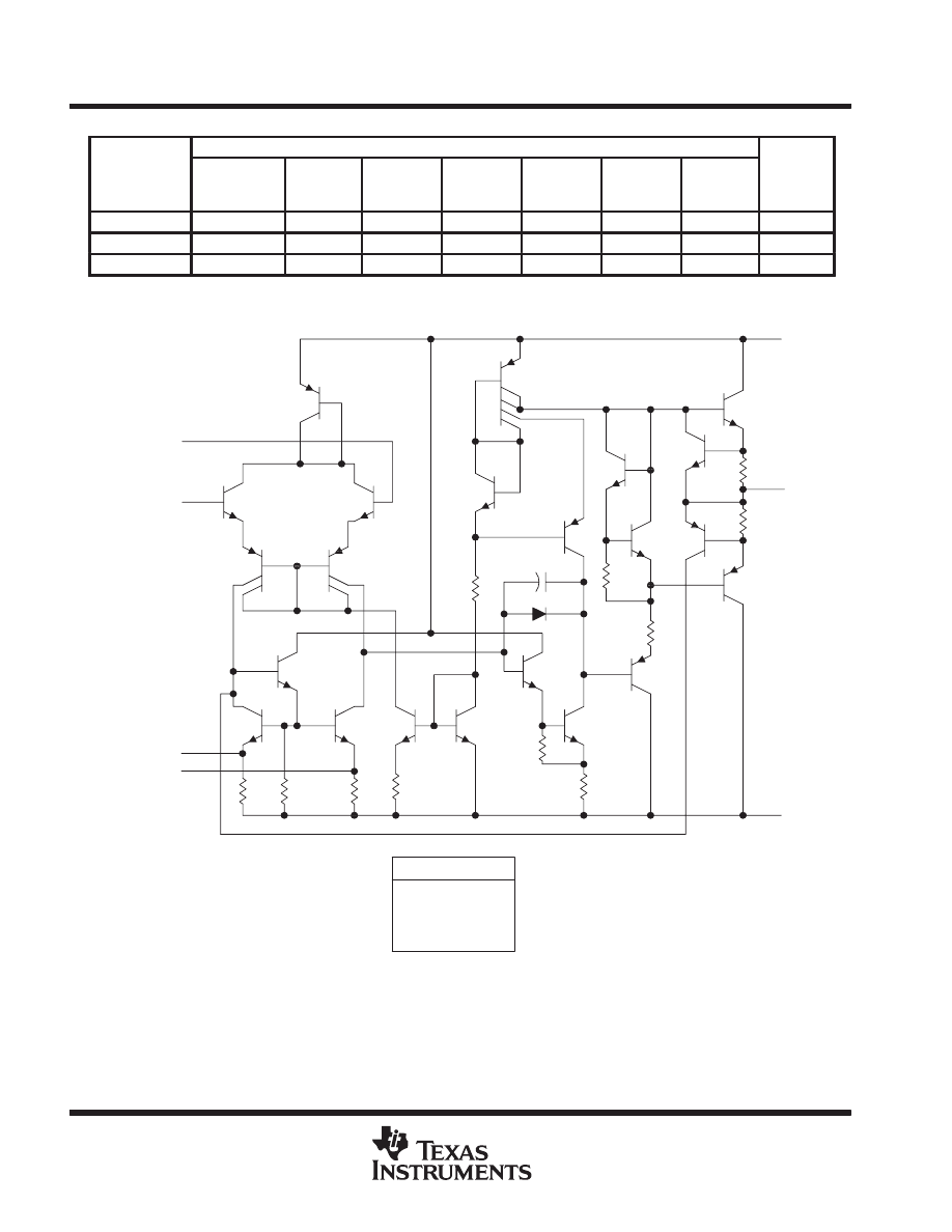
schematic
IN –
IN+
VCC+
VCC –
OUT
OFFSET N1
OFFSET N2
Transistors
22
Resistors
11
Diode
1
Capacitor
1
Component Count
µ
A741,
µ
A741Y
GENERAL-PURPOSE OPERATIONAL AMPLIFIERS
SLOS094A – NOVEMBER 1970 – REVISED JANUARY 1992
3
POST OFFICE BOX 655303
•
DALLAS, TEXAS 75265
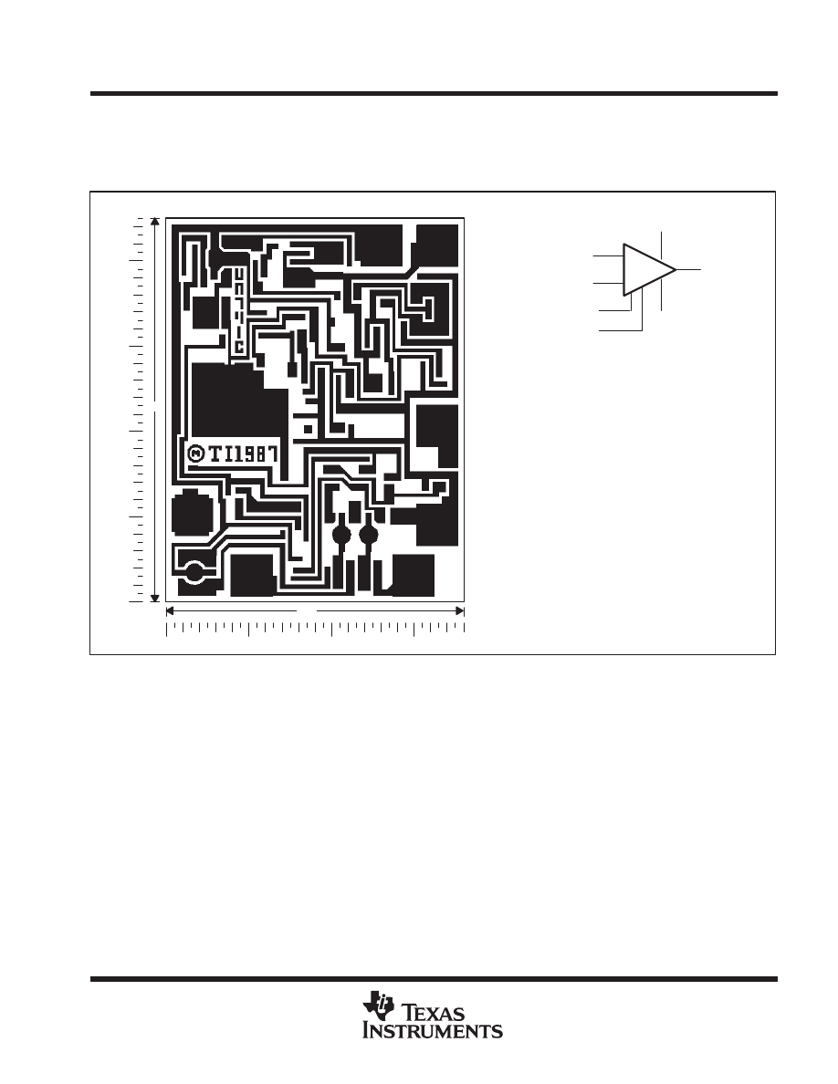
µ
A741Y chip information
This chip, when properly assembled, displays characteristics similar to the
µ
A741C. Thermal compression or
ultrasonic bonding may be used on the doped-aluminum bonding pads. Chips may be mounted with conductive
epoxy or a gold-silicon preform.
BONDING PAD ASSIGNMENTS
CHIP THICKNESS: 15 TYPICAL
BONDING PADS: 4
×
4 MINIMUM
TJmax = 150
°
C.
TOLERANCES ARE
±
10%.
ALL DIMENSIONS ARE IN MILS.
+
–
OUT
IN +
IN –
VCC+
(7)
(3)
(2)
(6)
(4)
VCC –
(5)
(1)
OFFSET N2
OFFSET N1
45
36
(1)
(8)
(7)
(6)
(5)
(4)
(3)
(2)
µ
A741,
µ
A741Y
GENERAL-PURPOSE OPERATIONAL AMPLIFIERS
SLOS094A – NOVEMBER 1970 – REVISED JANUARY 1992
4
POST OFFICE BOX 655303
•
DALLAS, TEXAS 75265
absolute maximum ratings over operating free-air temperature range (unless otherwise noted)
†
µ
A741C
µ
A741I
µ
A741M
UNIT
Supply voltage, VCC+ (see Note 1)
18
22
22
V
Supply voltage, VCC – (see Note 1)
–18
– 22
– 22
V
Differential input voltage, VID (see Note 2)
±
15
±
30
±
30
V
Input voltage, VI any input (see Notes 1 and 3)
±
15
±
15
±
15
V
Voltage between offset null (either OFFSET N1 or OFFSET N2) and VCC –
±
15
±
0.5
±
0.5
V
Duration of output short circuit (see Note 4)
unlimited
unlimited
unlimited
Continuous total power dissipation
See Dissipation Rating Table
Operating free-air temperature range, TA
0 to 70
– 40 to 85
– 55 to 125
°
C
Storage temperature range
– 65 to 150
– 65 to 150
– 65 to 150
°
C
Case temperature for 60 seconds
FK package
260
°
C
Lead temperature 1,6 mm (1/16 inch) from case for 60 seconds
J, JG, or U package
300
°
C
Lead temperature 1,6 mm (1/16 inch) from case for 10 seconds
D, P, or PW package
260
260
°
C
† Stresses beyond those listed under “absolute maximum ratings” may cause permanent damage to the device. These are stress ratings only, and
functional operation of the device at these or any other conditions beyond those indicated under “recommended operating conditions” is not
implied. Exposure to absolute-maximum-rated conditions for extended periods may affect device reliability.
NOTES:
1. All voltage values, unless otherwise noted, are with respect to the midpoint between VCC+ and VCC – .
2. Differential voltages are at IN+ with respect to IN –.
3. The magnitude of the input voltage must never exceed the magnitude of the supply voltage or 15 V, whichever is less.
4. The output may be shorted to ground or either power supply. For the
µ
A741M only, the unlimited duration of the short circuit applies
at (or below) 125
°
C case temperature or 75
°
C free-air temperature.
DISSIPATION RATING TABLE
PACKAGE
TA
≤
25
°
C
POWER RATING
DERATING
FACTOR
DERATE
ABOVE TA
TA = 70
°
C
POWER RATING
TA = 85
°
C
POWER RATING
TA = 125
°
C
POWER RATING
D
500 mW
5.8 mW/
°
C
64
°
C
464 mW
377 mW
N/A
FK
500 mW
11.0 mW/
°
C
105
°
C
500 mW
500 mW
275 mW
J
500 mW
11.0 mW/
°
C
105
°
C
500 mW
500 mW
275 mW
JG
500 mW
8.4 mW/
°
C
90
°
C
500 mW
500 mW
210 mW
P
500 mW
N/A
N/A
500 mW
500 mW
N/A
PW
525 mW
4.2 mW/
°
C
25
°
C
336 mW
N/A
N/A
U
500 mW
5.4 mW/
°
C
57
°
C
432 mW
351 mW
135 mW
µ
A741,
µ
A741Y
GENERAL-PURPOSE OPERATIONAL AMPLIFIERS
SLOS094A – NOVEMBER 1970 – REVISED JANUARY 1992
5
POST OFFICE BOX 655303
•
DALLAS, TEXAS 75265
electrical characteristics at specified free-air temperature, V
CC
±
=
±
15 V (unless otherwise noted)
PARAMETER
TEST
TA†
µ
A741C
µ
A741I,
µ
A741M
UNIT
PARAMETER
CONDITIONS
TA†
MIN
TYP
MAX
MIN
TYP
MAX
UNIT
VIO
Input offset voltage
VO = 0
25
°
C
1
6
1
5
mV
VIO
Input offset voltage
VO = 0
Full range
7.5
6
mV
∆
VIO(adj)
Offset voltage adjust range
VO = 0
25
°
C
±
15
±
15
mV
IIO
Input offset current
VO = 0
25
°
C
20
200
20
200
nA
IIO
Input offset current
VO = 0
Full range
300
500
nA
IIB
Input bias current
VO = 0
25
°
C
80
500
80
500
nA
IIB
Input bias current
VO = 0
Full range
800
1500
nA
VICR
Common-mode input
25
°
C
±
12
±
13
±
12
±
13
V
VICR
voltage range
Full range
±
12
±
12
V
RL = 10 k
Ω
25
°
C
±
12
±
14
±
12
±
14
VOM
Maximum peak output
RL
≥
10 k
Ω
Full range
±
12
±
12
V
VOM
voltage swing
RL = 2 k
Ω
25
°
C
±
10
±
13
±
10
±
13
V
RL
≥
2 k
Ω
Full range
±
10
±
10
AVD
Large-signal differential
RL
≥
2 k
Ω
25
°
C
20
200
50
200
V/mV
AVD
g
g
voltage amplification
VO =
±
10 V
Full range
15
25
V/mV
ri
Input resistance
25
°
C
0.3
2
0.3
2
M
Ω
ro
Output resistance
VO = 0, See Note 5
25
°
C
75
75
Ω
Ci
Input capacitance
25
°
C
1.4
1.4
pF
CMRR
Common-mode rejection
VIC = VICRmin
25
°
C
70
90
70
90
dB
CMRR
j
ratio
VIC = VICRmin
Full range
70
70
dB
kSVS
Supply voltage sensitivity
VCC =
±
9 V to
±
15 V
25
°
C
30
150
30
150
µ
V/V
kSVS
y
g
y
(
∆
VIO /
∆
VCC)
VCC =
±
9 V to
±
15 V
Full range
150
150
µ
V/V
IOS
Short-circuit output current
25
°
C
±
25
±
40
±
25
±
40
mA
ICC
Supply current
VO = 0
No load
25
°
C
1.7
2.8
1.7
2.8
mA
ICC
Supply current
VO = 0, No load
Full range
3.3
3.3
mA
PD
Total power dissipation
VO = 0
No load
25
°
C
50
85
50
85
mW
PD
Total power dissipation
VO = 0, No load
Full range
100
100
mW
† All characteristics are measured under open-loop conditions with zero common-mode input voltage unless otherwise specified. Full range for
the
µ
A741C is 0
°
C to 70
°
C, the
µ
A741I is – 40
°
C to 85
°
C, and the
µ
A741M is – 55
°
C to 125
°
C.
NOTE 5: This typical value applies only at frequencies above a few hundred hertz because of the effects of drift and thermal feedback.
operating characteristics, V
CC
±
=
±
15 V, T
A
= 25
°
C
PARAMETER
TEST CONDITIONS
µ
A741C
µ
A741I,
µ
A741M
UNIT
PARAMETER
TEST CONDITIONS
MIN
TYP
MAX
MIN
TYP
MAX
UNIT
tr
Rise time
VI = 20 mV,
RL = 2 k
Ω,
0.3
0.3
µ
s
Overshoot factor
I
,
CL = 100 pF,
L
,
See Figure 1
5%
5%
SR
Slew rate at unity gain
VI = 10 V,
CL = 100 pF,
RL = 2 k
Ω,
See Figure 1
0.5
0.5
V/
µ
s
µ
A741,
µ
A741Y
GENERAL-PURPOSE OPERATIONAL AMPLIFIERS
SLOS094A – NOVEMBER 1970 – REVISED JANUARY 1992
6
POST OFFICE BOX 655303
•
DALLAS, TEXAS 75265
electrical characteristics at specified free-air temperature, V
CC
±
=
±
15 V, T
A
= 25
°
C (unless
otherwise noted)
PARAMETER
TEST CONDITIONS
µ
A741Y
UNIT
PARAMETER
TEST CONDITIONS
MIN
TYP
MAX
UNIT
VIO
Input offset voltage
VO = 0
1
6
mV
∆
VIO(adj)
Offset voltage adjust range
VO = 0
±
15
mV
IIO
Input offset current
VO = 0
20
200
nA
IIB
Input bias current
VO = 0
80
500
nA
VICR
Common-mode input voltage range
±
12
±
13
V
VOM
Maximum peak output voltage swing
RL = 10 k
Ω
±
12
±
14
V
VOM
Maximum peak output voltage swing
RL = 2 k
Ω
±
10
±
13
V
AVD
Large-signal differential voltage amplification
RL
≥
2 k
Ω
20
200
V/mV
ri
Input resistance
0.3
2
M
Ω
ro
Output resistance
VO = 0, See Note 5
75
Ω
Ci
Input capacitance
1.4
pF
CMRR
Common-mode rejection ratio
VIC = VICRmin
70
90
dB
kSVS
Supply voltage sensitivity (
∆
VIO /
∆
VCC)
VCC =
±
9 V to
±
15 V
30
150
µ
V/V
IOS
Short-circuit output current
±
25
±
40
mA
ICC
Supply current
VO = 0, No load
1.7
2.8
mA
PD
Total power dissipation
VO = 0, No load
50
85
mW
† All characteristics are measured under open-loop conditions with zero common-mode voltage unless otherwise specified.
NOTE 5: This typical value applies only at frequencies above a few hundred hertz because of the effects of drift and thermal feedback.
operating characteristics, V
CC
±
=
±
15 V, T
A
= 25
°
C
PARAMETER
TEST CONDITIONS
µ
A741Y
UNIT
PARAMETER
TEST CONDITIONS
MIN
TYP
MAX
UNIT
tr
Rise time
VI = 20 mV,
RL = 2 k
Ω,
0.3
µ
s
Overshoot factor
I
,
CL = 100 pF,
L
,
See Figure 1
5%
SR
Slew rate at unity gain
VI = 10 V,
CL = 100 pF,
RL = 2 k
Ω,
See Figure 1
0.5
V/
µ
s
µ
A741,
µ
A741Y
GENERAL-PURPOSE OPERATIONAL AMPLIFIERS
SLOS094A – NOVEMBER 1970 – REVISED JANUARY 1992
7
POST OFFICE BOX 655303
•
DALLAS, TEXAS 75265
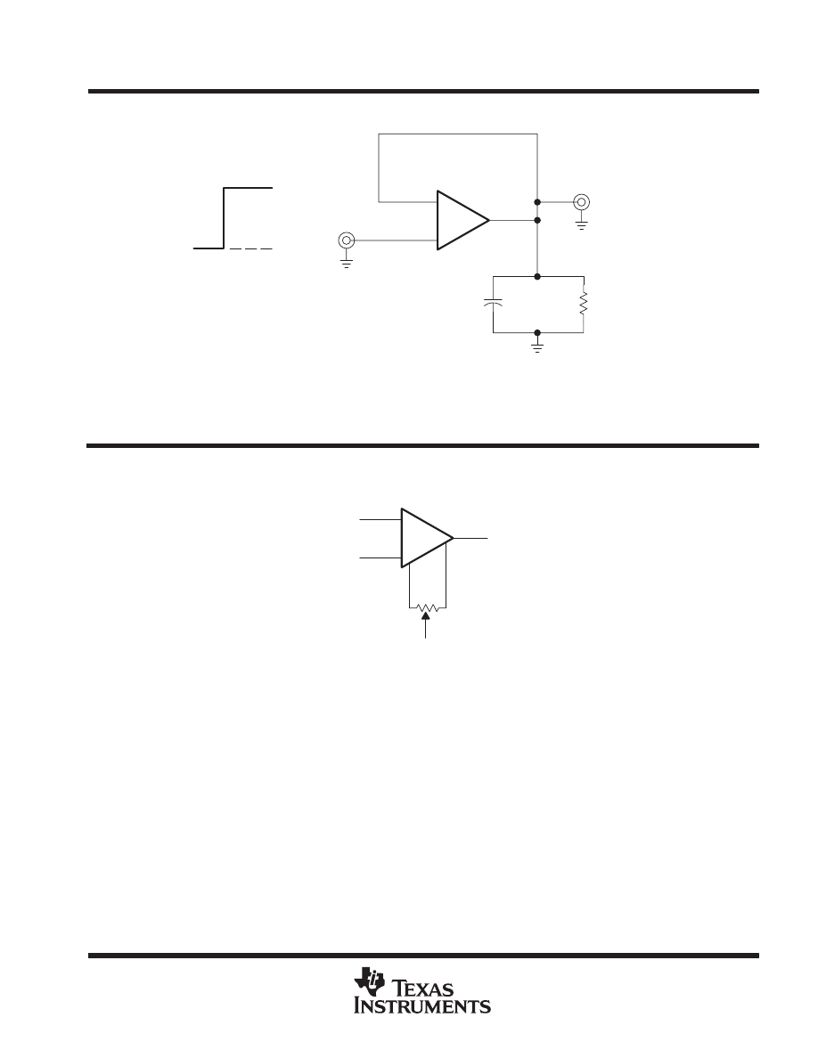
PARAMETER MEASUREMENT INFORMATION
INPUT VOLTAGE
WAVEFDORM
TEST CIRCUIT
RL = 2 k
Ω
CL = 100 pF
OUT
IN
+
–
0 V
VI
Figure 1. Rise Time, Overshoot, and Slew Rate
APPLICATION INFORMATION
Figure 2 shows a diagram for an input offset voltage null circuit.
To VCC –
OFFSET N1
10 k
Ω
OFFSET N2
+
–
OUT
IN +
IN –
Figure 2. Input Offset Voltage Null Circuit
µ
A741,
µ
A741Y
GENERAL-PURPOSE OPERATIONAL AMPLIFIERS
SLOS094A – NOVEMBER 1970 – REVISED JANUARY 1992
8
POST OFFICE BOX 655303
•
DALLAS, TEXAS 75265
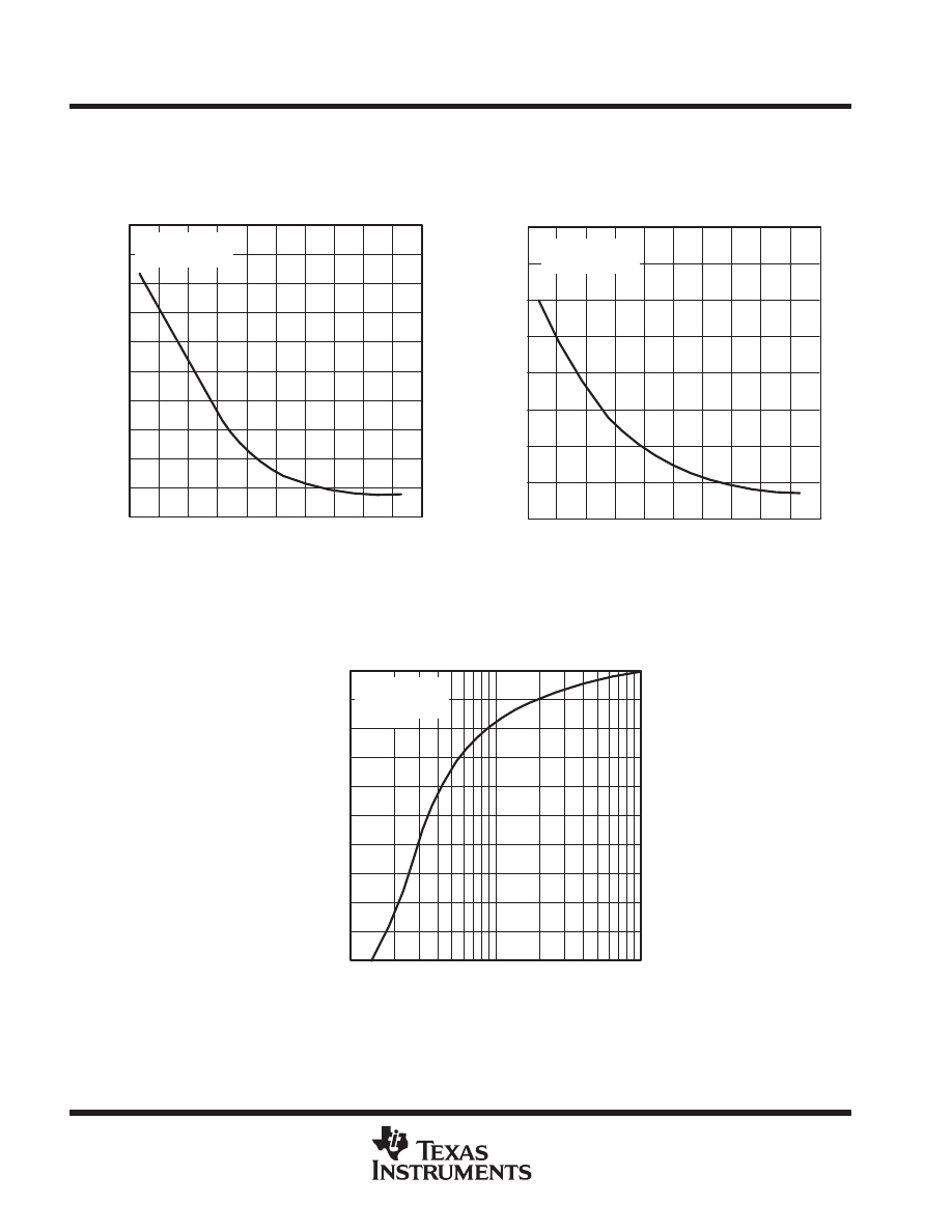
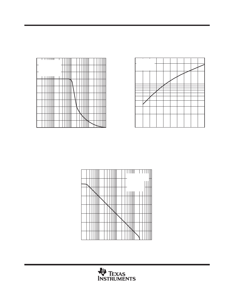
TYPICAL CHARACTERISTICS
†
Figure 3
I
TA – Free-Air Temperature –
°
C
120
80
40
0
– 40
20
INPUT OFFSET CURRENT
vs
FREE-AIR TEMPERATURE
IO
– Input Offset Current – nA
ÏÏÏÏÏ
ÏÏÏÏÏ
VCC – = –15 V
ÏÏÏÏÏ
ÏÏÏÏÏ
VCC+ = 15 V
90
70
50
30
10
0
40
60
80
100
– 60
– 20
20
60
100
140
Figure 4
400
300
200
100
0
0
40
80
120
TA – Free-Air Temperature –
°
C
I
INPUT BIAS CURRENT
vs
FREE-AIR TEMPERATURE
IB
– Input Bias Current – nA
ÏÏÏÏÏ
ÏÏÏÏÏ
VCC – = –15 V
ÏÏÏÏÏ
VCC+ = 15 V
350
250
150
50
– 40
– 60
– 20
20
60
100
140
V
RL – Load Resistance – k
Ω
10
7
4
2
1
0.7
0.4
0.2
0.1
±
4
±
5
±
6
±
7
±
8
±
9
±
10
±
11
±
12
±
13
±
14
MAXIMUM PEAK OUTPUT VOLTAGE
vs
LOAD RESISTANCE
VCC+ = 15 V
VCC – = –15 V
TA = 25
°
C
OM
– Maximum Peak Output V
oltage – V
Figure 5
† Data at high and low temperatures are applicable only within the rated operating free-air temperature ranges of the various devices.
µ
A741,
µ
A741Y
GENERAL-PURPOSE OPERATIONAL AMPLIFIERS
SLOS094A – NOVEMBER 1970 – REVISED JANUARY 1992
9
POST OFFICE BOX 655303
•
DALLAS, TEXAS 75265
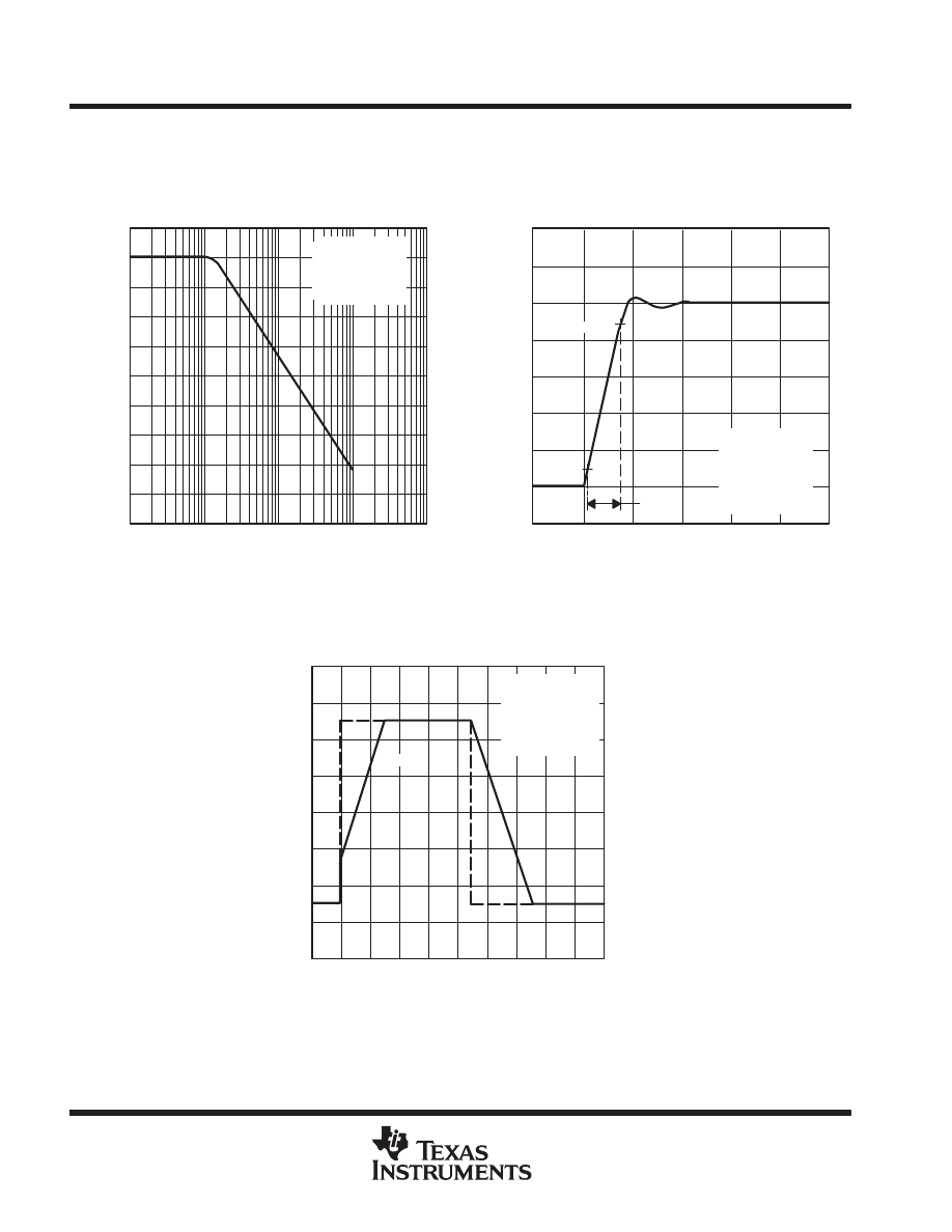
TYPICAL CHARACTERISTICS
Figure 6
V
±
20
f – Frequency – Hz
1 M
100 k
10 k
1 k
MAXIMUM PEAK OUTPUT VOLTAGE
vs
FREQUENCY
OM
– Maximum Peak Output V
oltage – V
±
18
±
16
±
14
±
12
±
10
±
8
±
6
±
4
±
2
0
VCC+ = 15 V
VCC – = –15 V
RL = 10 k
Ω
TA = 25
°
C
Figure 7
20
18
16
14
12
10
8
6
4
2
400
200
100
40
20
10
0
VCC
±
– Supply Voltage – V
OPEN-LOOP SIGNAL DIFFERENTIAL
VOLTAGE AMPLIFICATION
vs
SUPPLY VOLTAGE
VO =
±
10 V
RL = 2 k
Ω
TA = 25
°
C
A
VD
– Open-Loop Signal Differential
V
oltage
Amplification – V/mV
f – Frequency – Hz
10 M
1 M
10 k
100
1
10 –1
1
101
102
103
104
105
106
107
OPEN-LOOP LARGE-SIGNAL DIFFERENTIAL
VOLTAGE AMPLIFICATION
vs
FREQUENCY
VCC+ = 15 V
VCC – = –15 V
VO =
±
10 V
RL = 2 k
Ω
TA = 25
°
C
A
VD
– Open-Loop Signal Differential
V
oltage
Amplification – dB
Figure 8
µ
A741,
µ
A741Y
GENERAL-PURPOSE OPERATIONAL AMPLIFIERS
SLOS094A – NOVEMBER 1970 – REVISED JANUARY 1992
10
POST OFFICE BOX 655303
•
DALLAS, TEXAS 75265
TYPICAL CHARACTERISTICS
Figure 9
CMRR – Common-Mode Rejection Ratio – dB
f – Frequency – Hz
10 k
1 M
100 M
100
1
0
10
20
30
40
50
60
70
80
90
100
COMMON-MODE REJECTION RATIO
vs
FREQUENCY
VCC+ = 15 V
VCC– = –15 V
BS = 10 k
Ω
TA = 25
°
C
Figure 10
10%
tr
2.5
2
1.5
1
0.5
0
28
24
20
16
12
8
4
0
– Output V
oltage
–
mV
t – Time
± µ
s
–4
OUTPUT VOLTAGE
vs
ELAPSED TIME
V
O
ÏÏ
90%
VCC+ = 15 V
VCC– = –15 V
RL = 2 k
Ω
CL = 100 pF
TA = 25
°
C
8
6
4
2
0
– 2
– 4
– 6
90
80
70
60
50
40
30
20
10
0
Input and Output V
oltage – V
t – Time –
µ
s
– 8
VOLTAGE-FOLLOWER
LARGE-SIGNAL PULSE RESPONSE
VO
VI
VCC+ = 15 V
VCC– = –15 V
RL = 2 k
Ω
CL = 100 pF
TA = 25
°
C
Figure 11

IMPORTANT NOTICE
Texas Instruments and its subsidiaries (TI) reserve the right to make changes to their products or to discontinue
any product or service without notice, and advise customers to obtain the latest version of relevant information
to verify, before placing orders, that information being relied on is current and complete. All products are sold
subject to the terms and conditions of sale supplied at the time of order acknowledgement, including those
pertaining to warranty, patent infringement, and limitation of liability.
TI warrants performance of its semiconductor products to the specifications applicable at the time of sale in
accordance with TI’s standard warranty. Testing and other quality control techniques are utilized to the extent
TI deems necessary to support this warranty. Specific testing of all parameters of each device is not necessarily
performed, except those mandated by government requirements.
CERTAIN APPLICATIONS USING SEMICONDUCTOR PRODUCTS MAY INVOLVE POTENTIAL RISKS OF
DEATH, PERSONAL INJURY, OR SEVERE PROPERTY OR ENVIRONMENTAL DAMAGE (“CRITICAL
APPLICATIONS”). TI SEMICONDUCTOR PRODUCTS ARE NOT DESIGNED, AUTHORIZED, OR
WARRANTED TO BE SUITABLE FOR USE IN LIFE-SUPPORT DEVICES OR SYSTEMS OR OTHER
CRITICAL APPLICATIONS. INCLUSION OF TI PRODUCTS IN SUCH APPLICATIONS IS UNDERSTOOD TO
BE FULLY AT THE CUSTOMER’S RISK.
In order to minimize risks associated with the customer’s applications, adequate design and operating
safeguards must be provided by the customer to minimize inherent or procedural hazards.
TI assumes no liability for applications assistance or customer product design. TI does not warrant or represent
that any license, either express or implied, is granted under any patent right, copyright, mask work right, or other
intellectual property right of TI covering or relating to any combination, machine, or process in which such
semiconductor products or services might be or are used. TI’s publication of information regarding any third
party’s products or services does not constitute TI’s approval, warranty or endorsement thereof.
Copyright
1998, Texas Instruments Incorporated

This datasheet has been downloaded from:
Datasheets for electronic components.
Wyszukiwarka
Podobne podstrony:
4063 (Texas Instruments) id 384 Nieznany (2)
NE555 Texas Instruments id 3161 Nieznany
Instruktazstanowiskowy id 21769 Nieznany
kolm instrumenty 3 id 239529 Nieznany
cw3 i 4 instrukcja id 123316 Nieznany
algorytmy PKI Instrukcja id 577 Nieznany (2)
instrukcja 3 id 215628 Nieznany
Instrukcja 3 2 id 215652 Nieznany
cwiczenie 3 instrukcja id 12533 Nieznany
Cwicz 22 2 instrukcja id 124025 Nieznany
Lab2 Instrukcja id 259301 Nieznany
Pik INSTRUKCJA id 358072 Nieznany
cw 05 instrukcja id 121376 Nieznany
Instrukcja 4 id 215662 Nieznany
Instrukcja 2 3 id 215492 Nieznany
lab1 Instrukcja id 750240 Nieznany
GZK0 instrukcja id 198229 Nieznany
ACCES Instrukcja id 614317 Nieznany (2)
Instrukcja 9 id 215530 Nieznany
więcej podobnych podstron