_______________General Description
The MAX038 is a high-frequency, precision function
generator producing accurate, high-frequency triangle,
sawtooth, sine, square, and pulse waveforms with a
minimum of external components. The output frequency
can be controlled over a frequency range of 0.1Hz to
20MHz by an internal 2.5V bandgap voltage
reference and an external resistor and capacitor. The
duty cycle can be varied over a wide range by applying
a ±2.3V control signal, facilitating pulse-width modula-
tion and the generation of sawtooth waveforms.
Frequency modulation and frequency sweeping are
achieved in the same way. The duty cycle and
frequency controls are independent.
Sine, square, or triangle waveforms can be selected at
the output by setting the appropriate code at two
TTL-compatible select pins. The output signal for all
waveforms is a 2V
P-P
signal that is symmetrical around
ground. The low-impedance output can drive up
to ±20mA.
The TTL-compatible SYNC output from the internal
oscillator maintains a 50% duty cycle—regardless of
the duty cycle of the other waveforms—to synchronize
other devices in the system. The internal oscillator can
be synchronized to an external TTL clock connected
to PDI.
________________________Applications
Precision Function Generators
Voltage-Controlled Oscillators
Frequency Modulators
Pulse-Width Modulators
Phase-Locked Loops
Frequency Synthesizer
FSK Generator—Sine and Square Waves
____________________________Features
♦
0.1Hz to 20MHz Operating Frequency Range
♦
Triangle, Sawtooth, Sine, Square, and Pulse
Waveforms
♦
Independent Frequency and Duty-Cycle
Adjustments
♦
350 to 1 Frequency Sweep Range
♦
15% to 85% Variable Duty Cycle
♦
Low-Impedance Output Buffer: 0.1
Ω
♦
Low-Distortion Sine Wave: 0.75%
♦
Low 200ppm/°C Temperature Drift
______________Ordering Information
*
Contact factory for dice specifications.
MAX038
High-Frequency Waveform Generator
________________________________________________________________
Maxim Integrated Products
1
20
19
18
17
16
15
14
13
12
11
1
2
3
4
5
6
7
8
9
10
V-
OUT
GND
V+
A1
A0
GND
REF
TOP VIEW
MAX038
DV+
DGND
SYNC
PDI
FADJ
DADJ
GND
COSC
PDO
GND
IIN
GND
DIP/SO
__________________Pin Configuration
19-0266; Rev 2a; 9/96
PART
TEMP. RANGE
PIN-PACKAGE
MAX038CPP
0°C to +70°C
20 Plastic DIP
MAX038CWP
0°C to +70°C
20 SO
MAX038C/D
0°C to +70°C
Dice*
MAX038EPP
-40°C to +85°C
20 Plastic DIP
MAX038EWP
-40°C to +85°C
20 SO
EVALUATION KIT
AVAILABLE
For free samples & the latest literature: http://www.maxim-ic.com, or phone 1-800-998-8800.
For small orders, phone 408-737-7600 ext. 3468.
MAX038
High-Frequency Waveform Generator
2
_______________________________________________________________________________________
ABSOLUTE MAXIMUM RATINGS
ELECTRICAL CHARACTERISTICS
(Circuit of Figure 1, GND = DGND = 0V, V+ = DV+ = 5V, V- = -5V, V
DADJ
= V
FADJ
= V
PDI
= V
PDO
= 0V, C
F
= 100pF,
R
IN
= 25k
Ω
, R
L
= 1k
Ω
, C
L
= 20pF, T
A
= T
MIN
to T
MAX
, unless otherwise noted. Typical values are at T
A
= +25°C.)
Stresses beyond those listed under “Absolute Maximum Ratings” may cause permanent damage to the device. These are stress ratings only, and functional
operation of the device at these or any other conditions beyond those indicated in the operational sections of the specifications is not implied. Exposure to
absolute maximum rating conditions for extended periods may affect device reliability.
PARAMETER
SYMBOL
MIN
TYP
MAX
UNITS
Frequency Temperature
Coefficient
∆
F
o
/°C
200
ppm/°C
600
IIN Offset Voltage
V
IN
±1.0
±2.0
mV
Frequency Programming
Current
I
IN
1.25
375
µA
(
∆
F
o
/F
o
)
∆
V+
±0.4
±2.00
Frequency Power-Supply
Rejection
(
∆
F
o
/F
o
)
∆
V-
±0.2
±1.00
%/V
Output Peak-to-Peak Symmetry
V
OUT
±4
mV
Maximum Operating Frequency
F
o
20.0
40.0
MHz
2.50
750
Output Resistance
R
OUT
0.1
0.2
Ω
Output Short-Circuit Current
I
OUT
40
mA
Amplitude
V
OUT
1.9
2.0
2.1
V
P-P
Rise Time
t
R
12
ns
Fall Time
t
F
12
ns
Duty Cycle
dc
47
50
53
%
Amplitude
V
OUT
1.9
2.0
2.1
V
P-P
Nonlinearity
0.5
%
Duty Cycle
dc
47
50
53
%
CONDITIONS
V
FADJ
= -3V
V
FADJ
= 0V
V
FADJ
= -3V
V- = -5V, V+ = 4.75V to 5.25V
V+ = 5V, V- = -4.75V to -5.25V
Short circuit to GND
10% to 90%
90% to 10%
V
DADJ
= 0V, dc = t
ON
/t x 100%
15pCF
≤
15pF, I
IN
= 500µA
V
FADJ
= 0V
F
o
= 100kHz, 5% to 95%
V
DADJ
= 0V (Note 1)
V+ to GND ................................................................-0.3V to +6V
DV+ to DGND...........................................................-0.3V to +6V
V- to GND .................................................................+0.3V to -6V
Pin Voltages
IIN, FADJ, DADJ, PDO .....................(V- - 0.3V) to (V+ + 0.3V)
COSC .....................................................................+0.3V to V-
A0, A1, PDI, SYNC, REF.........................................-0.3V to V+
GND to DGND ................................................................±0.3V
Maximum Current into Any Pin .........................................±50mA
OUT, REF Short-Circuit Duration to GND, V+, V- ...............30sec
Continuous Power Dissipation (T
A
= +70°C)
Plastic DIP (derate 11.11mW/°C above +70°C) ..........889mW
SO (derate 10.00mW/°C above +70°C) .......................800mW
CERDIP (derate 11.11mW/°C above +70°C) ...............889mW
Operating Temperature Ranges
MAX038C_ _ .......................................................0°C to +70°C
MAX038E_ _ ....................................................-40°C to +85°C
Maximum Junction Temperature .....................................+150°C
Storage Temperature Range .............................-65°C to +150°C
Lead Temperature (soldering, 10sec) .............................+300°C
Amplitude
V
OUT
1.9
2.0
2.1
V
P-P
Duty cycle adjusted to 50%
0.75
Total Harmonic Distortion
THD
Duty cycle unadjusted
1.50
%
F
o
/°C
FREQUENCY CHARACTERISTICS
OUTPUT AMPLIFIER (applies to all waveforms)
SQUARE-WAVE OUTPUT (R
L
= 100
Ω
)
TRIANGLE-WAVE OUTPUT (R
L
= 100
Ω
)
SINE-WAVE OUTPUT (R
L
= 100
Ω
)
MAX038
High-Frequency Waveform Generator
_______________________________________________________________________________________
3
ELECTRICAL CHARACTERISTICS (continued)
(Circuit of Figure 1, GND = DGND = 0V, V+ = DV+ = 5V, V- = -5V, V
DADJ
= V
FADJ
= V
PDI
= V
PDO
= 0V, C
F
= 100pF,
R
IN
= 25k
Ω
, R
L
= 1k
Ω
, C
L
= 20pF, T
A
= T
MIN
to T
MAX
, unless otherwise noted. Typical values are at T
A
= +25°C.)
Note 1:
Guaranteed by duty-cycle test on square wave.
Note 2:
V
REF
is independent of V-.
PARAMETER
DADJ Nonlinearity
SYMBOL
MIN
TYP
MAX
dc/V
FADJ
2
4
UNITS
%
Duty Cycle
dc
SYNC
50
%
Fall Time
t
F
10
ns
Rise Time
t
R
10
ns
Change in Output Frequency
with DADJ
DADJ Input Current
I
DADJ
190
250
320
µA
DADJ Voltage Range
V
DADJ
±2.3
V
F
o
/V
DADJ
±2.5
±8
%
Duty-Cycle Adjustment Range
dc
15
85
%
Maximum DADJ Modulating
Frequency
F
DC
2
MHz
Output Low Voltage
FADJ Input Current
I
FADJ
190
250
320
µA
FADJ Voltage Range
V
FADJ
±2.4
V
Frequency Sweep Range
V
OL
0.3
0.4
V
F
o
±70
%
FM Nonlinearity with FADJ
Output High Voltage
F
o
/V
FADJ
±0.2
%
V
OH
2.8
3.5
V
Change in Duty Cycle with FADJ
dc/V
FADJ
±2
%
Output Voltage
V
REF
2.48
2.50
2.52
V
CONDITIONS
-2V
≤
V
DADJ
≤
2V
90% to 10%, R
L
= 3k
Ω
, C
L
= 15pF
10% to 90%, R
L
= 3k
Ω
, C
L
= 15pF
-2V
≤
V
DADJ
≤
2V
-2.3V
≤
V
DADJ
≤
2.3V
I
SINK
= 3.2mA
-2.4V
≤
V
FADJ
≤
2.4V
-2V
≤
V
FADJ
≤
2V
I
SOURCE
= 400µA
-2V
≤
V
FADJ
≤
2V
I
REF
= 0
Temperature Coefficient
V
REF
/°C
20
ppm/°C
0mA
≤
I
REF
≤
4mA (source)
1
2
Load Regulation
V
REF
/I
REF
-100µA
≤
I
REF
≤
0µA (sink)
1
4
mV/mA
Line Regulation
V
REF
/V+
4.75V
≤
V+
≤
5.25V (Note 2)
1
2
mV/V
Input Low Voltage
V
IL
0.8
V
Input High Voltage
V
IH
2.4
V
Input Current (A0, A1)
I
IL
, I
IH
V
A0
, V
A1
= V
IL
, V
IH
±5
µA
Input Current (PDI)
I
IL
, I
IH
V
PDI
= V
IL
, V
IH
±25
µA
Positive Supply Voltage
V+
4.75
5.25
V
SYNC Supply Voltage
DV+
4.75
5.25
V
Negative Supply Voltage
V-
-4.75
-5.25
V
Positive Supply Current
I+
35
45
mA
SYNC Supply Current
I
DV+
1
2
mA
Negative Supply Current
I-
45
55
mA
Maximum FADJ Modulating
Frequency
F
F
2
MHz
SYNC OUTPUT
DUTY-CYCLE ADJUSTMENT (DADJ)
FREQUENCY ADJUSTMENT (FADJ)
VOLTAGE REFERENCE
LOGIC INPUTS (A0, A1, PDI)
POWER SUPPLY
MAX038
High-Frequency Waveform Generator
4
_______________________________________________________________________________________
__________________________________________Typical Operating Characteristics
(Circuit of Figure 1, V+ = DV+ = 5V, V- = -5V, V
DADJ
= V
FADJ
= V
PDI
= V
PDO
= 0V, R
L
= 1k
Ω
, C
L
= 20pF, T
A
= +25°C, unless
otherwise noted.)
0.1
1
100
1000
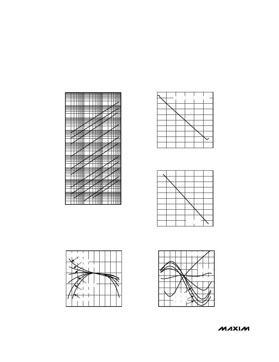
OUTPUT FREQUENCY
vs. IIN CURRENT
10
100
MAX038-08
IIN CURRENT (
µ
A)
OUTPUT FREQUENCY (Hz)
10
1
1k
10k
100k
1M
10M
100M
100
µ
F
47
µ
F
10
µ
F
3.3
µ
F
1
µ
F
100nF
33nF
3.3nF
330pF
100pF
33pF
1.0
0
-3
2
NORMALIZED OUTPUT FREQUENCY
vs. FADJ VOLTAGE
0.2
0.8
MAX038-09
V
FADJ
(V)
F
OUT
NORMALIZED
0
0.4
-2
-1
1
0.6
3
1.2
1.4
1.6
1.8
2.0
I
IN
= 100
µ
A, COSC = 1000pF
0.85
NORMALIZED OUTPUT FREQUENCY
vs. DADJ VOLTAGE
0.90
1.10
MAX038-17
DADJ (V)
NORMALIZED OUTPUT FREQUENCY
1.00
0.95
1.05
I
IN
= 10
µ
A
I
IN
= 25
µ
A
I
IN
= 50
µ
A
I
IN
= 100
µ
A
I
IN
= 250
µ
A
I
IN
= 500
µ
A
2.0
-2.5
-2.0
-1.0
1.0
2.5
DUTY-CYCLE LINEARITY
vs. DADJ VOLTAGE
-2.0
1.0
MAX038-18
DADJ
(V)
DUTY-CYCLE LINEARITY ERROR (%)
0
1.5
0
-1.0
-1.5
-0.5
0.5
1.5
I
IN
= 10
µ
A
I
IN
= 25
µ
A
I
IN
= 50
µ
A
I
IN
= 100
µ
A
I
IN
= 250
µ
A
I
IN
= 500
µ
A
60
0
-3
2
DUTY CYCLE vs. DADJ VOLTAGE
10
50
MAX038-16B
DADJ (V)
DUTY CYCLE (%)
0
30
20
-2
-1
1
40
70
80
90
100
3
I
IN
= 200
µ
A
MAX038
High-Frequency Waveform Generator
_______________________________________________________________________________________
5
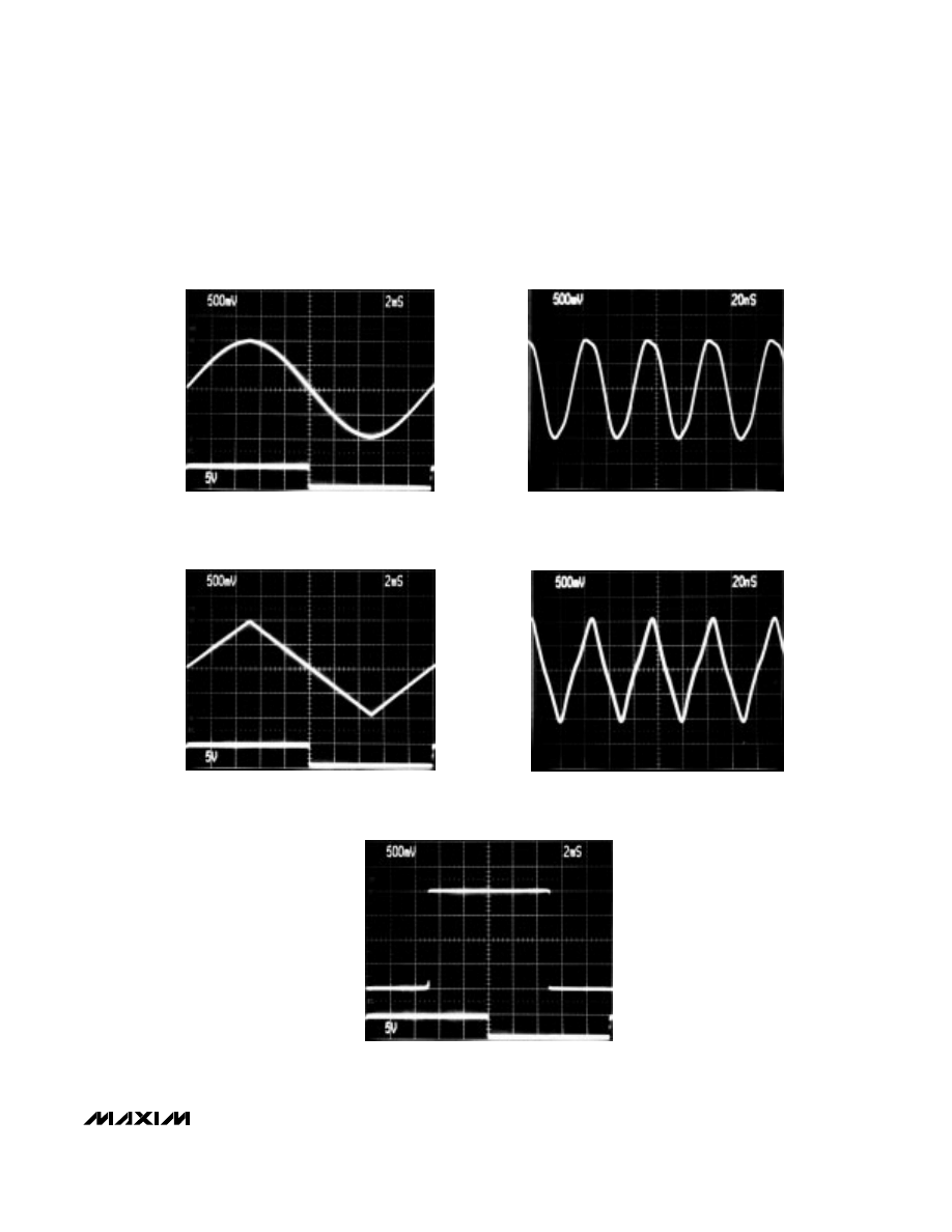
SINE-WAVE OUTPUT (50Hz)
TOP: OUTPUT 50Hz = F
o
BOTTOM: SYNC
I
IN
= 50
µ
A
C
F
= 1
µ
F
TRIANGLE-WAVE OUTPUT (50Hz)
TOP: OUTPUT 50Hz = F
o
BOTTOM: SYNC
I
IN
= 50
µ
A
C
F
= 1
µ
F
SQUARE-WAVE OUTPUT (50Hz)
TOP: OUTPUT 50Hz = F
o
BOTTOM: SYNC
I
IN
= 50
µ
A
C
F
= 1
µ
F
SINE-WAVE OUTPUT (20MHz)
I
IN
= 400
µ
A
C
F
= 20pF
____________________________Typical Operating Characteristics (continued)
(Circuit of Figure 1, V+ = DV+ = 5V, V- = -5V, V
DADJ
= V
FADJ
= V
PDI
= V
PDO
= 0V, R
L
= 1k
Ω
, C
L
= 20pF, T
A
= +25°C, unless
otherwise noted.)
TRIANGLE-WAVE OUTPUT (20MHz)
I
IN
= 400
µ
A
C
F
= 20pF
MAX038
High-Frequency Waveform Generator
6
_______________________________________________________________________________________
____________________________Typical Operating Characteristics (continued)
(Circuit of Figure 1, V+ = DV+ = 5V, V- = -5V, V
DADJ
= V
FADJ
= V
PDI
= V
PDO
= 0V, R
L
= 1k
Ω
, C
L
= 20pF, T
A
= +25°C, unless
otherwise noted.)
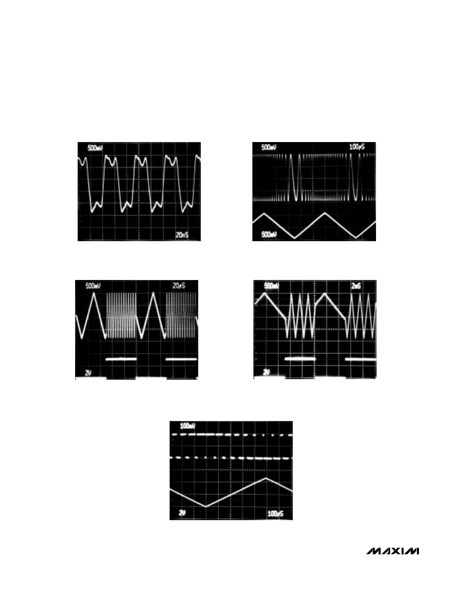
FREQUENCY MODULATION USING FADJ
TOP: OUTPUT
BOTTOM: FADJ
0.5V
0
-0.5V
FREQUENCY MODULATION USING I
IN
TOP: OUTPUT
BOTTOM: I
IN
FREQUENCY MODULATION USING I
IN
TOP: OUTPUT
BOTTOM: I
IN
PULSE-WIDTH MODULATION USING DADJ
TOP: SQUARE-WAVE OUT, 2V
P-P
BOTTOM: V
DADJ,
-2V to +2.3V
+1V
0V
-1V
+2V
0V
-2V
SQUARE-WAVE OUTPUT (20MHz)
I
IN
= 400
µ
A
C
F
= 20pF
MAX038
High-Frequency Waveform Generator
_______________________________________________________________________________________
7
______________________________________________________________Pin Description
*
The five GND pins are not internally connected. Connect all five GND pins to a quiet ground close to the device. A ground plane is
recommended (see
Layout Considerations).
0
-100
0
20
60
100
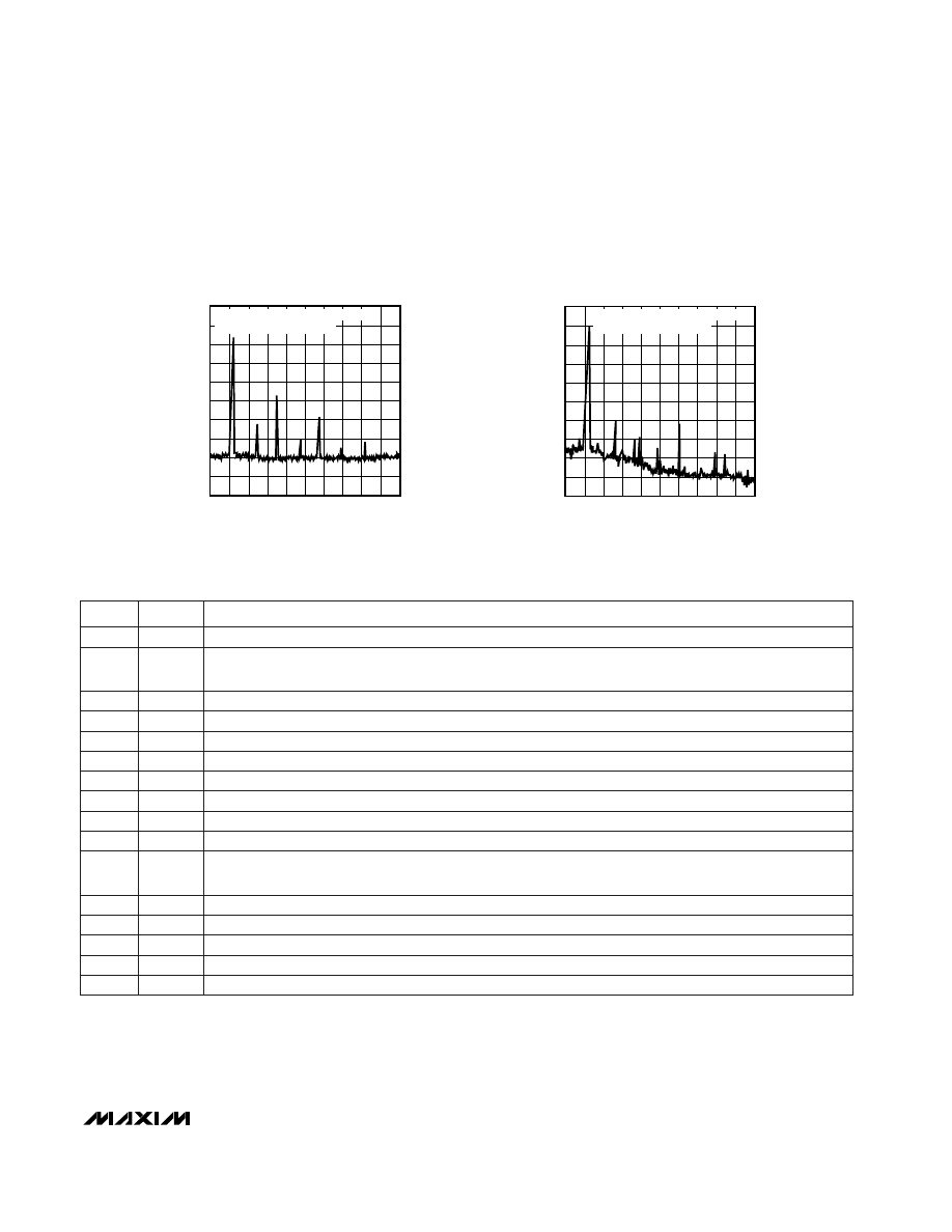
OUTPUT SPECTRUM, SINE WAVE
(F
o
= 11.5MHz)
-80
-20
MAX038-12A
FREQUENCY (MHz)
ATTENUATION (dB)
40
80
-40
-60
-10
-30
-50
-70
-90
10
30
50
70
90
R
IN
= 15k
Ω
(V
IN
= 2.5V), C
F
= 20pF,
V
DADJ
= 40mV, V
FADJ
= -3V
0
-100
0
10
30
50
OUTPUT SPECTRUM, SINE WAVE
(F
o
= 5.9kHz)
-80
-20
MAX038
12B
FREQUENCY (kHz)
ATTENUATION (dB)
20
40
-40
-60
-10
-30
-50
-70
-90
5
15
25
35
45
R
IN
= 51k
Ω
(V
IN
= 2.5V), C
F
= 0.01
µ
F,
V
DADJ
= 50mV, V
FADJ
= 0V
____________________________Typical Operating Characteristics (continued)
(Circuit of Figure 1, V+ = DV+ = 5V, V- = -5V, V
DADJ
= V
FADJ
= V
PDI
= V
PDO
= 0V, R
L
= 1k
Ω
, C
L
= 20pF, T
A
= +25°C, unless
otherwise noted.)
-5V supply input
V-
20
Sine, square, or triangle output
OUT
19
+5V supply input
V+
17
Digital +5V supply input. Can be left open if SYNC is not used.
DV+
16
Digital ground
DGND
15
TTL/CMOS-compatible output, referenced between DGND and DV+. Permits the internal oscillator to be
synchronized with an external signal. Leave open if unused.
SYNC
14
Current input for frequency control
IIN
10
Phase detector output. Connect to GND if phase detector is not used.
PDO
12
Phase detector reference clock input. Connect to GND if phase detector is not used.
PDI
13
External capacitor connection
COSC
5
Duty-cycle adjust input
DADJ
7
Frequency adjust input
FADJ
8
Waveform selection input; TTL/CMOS compatible
A1
4
Waveform selection input; TTL/CMOS compatible
A0
3
PIN
Ground*
GND
2, 6, 9,
11, 18
2.50V bandgap voltage reference output
REF
1
FUNCTION
NAME
MAX038
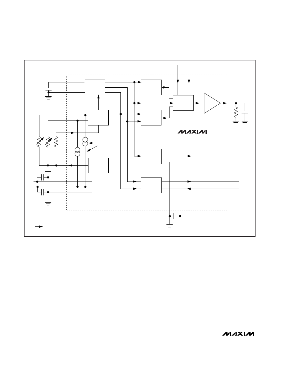
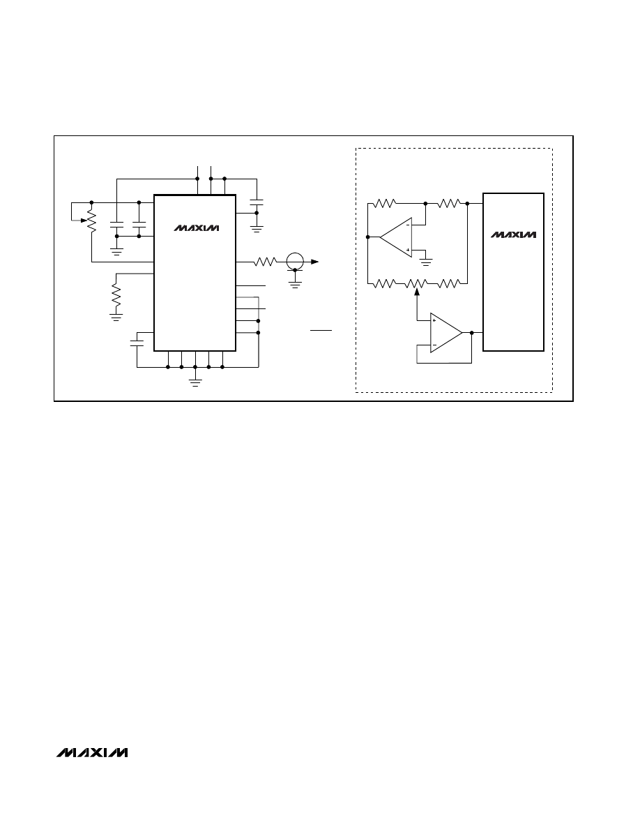
_______________Detailed Description
The MAX038 is a high-frequency function generator
that produces low-distortion sine, triangle, sawtooth, or
square (pulse) waveforms at frequencies from less than
1Hz to 20MHz or more, using a minimum of external
components. Frequency and duty cycle can be inde-
pendently controlled by programming the current, volt-
age, or resistance. The desired output waveform is
selected under logic control by setting the appropriate
code at the A0 and A1 inputs. A SYNC output and
phase detector are included to simplify designs requir-
ing tracking to an external signal source.
The MAX038 operates with ±5V ±5% power supplies.
The basic oscillator is a relaxation type that operates by
alternately charging and discharging a capacitor, C
F
,
with constant currents, simultaneously producing a tri-
angle wave and a square wave (Figure 1). The charg-
ing and discharging currents are controlled by the cur-
rent flowing into IIN, and are modulated by the voltages
applied to FADJ and DADJ. The current into IIN can be
varied from 2µA to 750µA, producing more than two
decades of frequency for any value of C
F
. Applying
±2.4V to FADJ changes the nominal frequency (with
V
FADJ
= 0V) by ±70%; this procedure can be used for
fine control.
Duty cycle (the percentage of time that the output wave-
form is positive) can be controlled from 10% to 90% by
applying ±2.3V to DADJ. This voltage changes the C
F
charging and discharging current ratio while maintaining
nearly constant frequency.
High-Frequency Waveform Generator
8
_______________________________________________________________________________________
MAX038
OSCILLATOR
OSCILLATOR
CURRENT
GENERATOR
2.5V
VOLTAGE
REFERENCE
OSC B
OSC A
TRIANGLE
SINE
SHAPER
COMPARATOR
COMPARATOR
PHASE
DETECTOR
MUX
COSC
GND
5
6
C
F
8
7
10
FADJ
DADJ
IIN
REF
1
17
20
2, 9, 11, 18
V+
V-
GND
R
F
R
D
R
IN
+5V
-5V
-250
µ
A
SINE
TRIANGLE
SQUARE
A0
A1
OUT
SYNC
PDO
PDI
19
14
12
13
R
L
C
L
3
4
DGND
DV+
15
16
+5V
*
=
SIGNAL DIRECTION, NOT POLARITY
= BYPASS CAPACITORS ARE 1
µ
F CERAMIC OR 1
µ
F ELECTROLYTIC IN PARALLEL WITH 1nF CERAMIC.
*
*
Figure 1. Block Diagram and Basic Operating Circuit
A stable 2.5V reference voltage, REF, allows simple
determination of IIN, FADJ, or DADJ with fixed resistors,
and permits adjustable operation when potentiometers
are connected from each of these inputs to REF. FADJ
and/or DADJ can be grounded, producing the nominal
frequency with a 50% duty cycle.
The output frequency is inversely proportional to
capacitor C
F
. C
F
values can be selected to produce
frequencies above 20MHz.
A sine-shaping circuit converts the oscillator triangle
wave into a low-distortion sine wave with constant
amplitude. The triangle, square, and sine waves are
input to a multiplexer. Two address lines, A0 and A1,
control which of the three waveforms is selected. The
output amplifier produces a constant 2V
P-P
amplitude
(±1V), regardless of wave shape or frequency.
The triangle wave is also sent to a comparator that pro-
duces a high-speed square-wave SYNC waveform that
can be used to synchronize other oscillators. The SYNC
circuit has separate power-supply leads and can be
disabled.
Two other phase-quadrature square waves are gener-
ated in the basic oscillator and sent to one side of an
“exclusive-OR” phase detector. The other side of the
phase-detector input (PDI) can be connected to an
external oscillator. The phase-detector output (PDO) is
a current source that can be connected directly to
FADJ to synchronize the MAX038 with the external
oscillator.
Waveform Selection
The MAX038 can produce either sine, square, or trian-
gle waveforms. The TTL/CMOS-logic address pins (A0
and A1) set the waveform, as shown below:
X = Don’t care
Waveform switching can be done at any time, without
regard to the phase of the output. Switching occurs
within 0.3µs, but there may be a small transient in the
output waveform that lasts 0.5µs.
Waveform Timing
Output Frequency
The output frequency is determined by the current
injected into the IIN pin, the COSC capacitance (to
ground), and the voltage on the FADJ pin. When
V
FADJ
= 0V, the fundamental output frequency (F
o
) is
given by the formula:
F
o
(MHz) = I
IN
(µA) ÷ C
F
(pF)
[1]
The period (t
o
) is:
t
o
(µs) = C
F
(pF) ÷ I
IN
(µA)
[2]
where:
I
IN
= current injected into IIN (between 2µA and
750µA)
C
F
= capacitance connected to COSC and GND
(20pF to >100µF).
For example:
0.5MHz = 100µA ÷ 200pF
and
2µs = 200pF ÷ 100µA
Optimum performance is achieved with I
IN
between
10µA and 400µA, although linearity is good with I
IN
between 2µA and 750µA. Current levels outside of this
range are not recommended. For fixed-frequency oper-
ation, set I
IN
to approximately 100µA and select a suit-
able capacitor value. This current produces the lowest
temperature coefficient, and produces the lowest fre-
quency shift when varying the duty cycle.
The capacitance can range from 20pF to more than
100µF, but stray circuit capacitance must be minimized
by using short traces. Surround the COSC pin and the
trace leading to it with a ground plane to minimize cou-
pling of extraneous signals to this node. Oscillation
above 20MHz is possible, but waveform distortion
increases under these conditions. The low frequency
limit is set by the leakage of the COSC capacitor and
by the required accuracy of the output frequency.
Lowest frequency operation with good accuracy is usu-
ally achieved with 10µF or greater non-polarized
capacitors.
An internal closed-loop amplifier forces IIN to virtual
ground, with an input offset voltage less than ±2mV. IIN
may be driven with either a current source (I
IN
), or a
voltage (V
IN
) in series with a resistor (R
IN
). (A resistor
between REF and IIN provides a convenient method of
generating I
IN
: I
IN
= V
REF
/R
IN
.) When using a voltage
in series with a resistor, the formula for the oscillator fre-
quency is:
F
o
(MHz) = V
IN
÷ [R
IN
x C
F
(pF)]
[3]
and:
t
o
(µs) = C
F
(pF) x R
IN
÷ V
IN
[4]
MAX038
High-Frequency Waveform Generator
_______________________________________________________________________________________
9
A0
A1
WAVEFORM
X
1
Sine wave
0
0
Square wave
1
0
Triangle wave

MAX038
When the MAX038’s frequency is controlled by a volt-
age source (V
IN
) in series with a fixed resistor (R
IN
), the
output frequency is a direct function of V
IN
as shown in
the above equations. Varying V
IN
modulates the oscilla-
tor frequency. For example, using a 10k
Ω
resistor for
R
IN
and sweeping V
IN
from 20mV to 7.5V produces
large frequency deviations (up to 375:1). Select R
IN
so
that I
IN
stays within the 2µA to 750µA range. The band-
width of the IIN control amplifier, which limits the modu-
lating signal’s highest frequency, is typically 2MHz.
IIN can be used as a summing point to add or subtract
currents from several sources. This allows the output
frequency to be a function of the sum of several vari-
ables. As V
IN
approaches 0V, the I
IN
error increases
due to the offset voltage of IIN.
Output frequency will be offset 1% from its final value
for 10 seconds after power-up.
FADJ Input
The output frequency can be modulated by FADJ,
which is intended principally for fine frequency control,
usually inside phase-locked loops. Once the funda-
mental, or center frequency (F
o
) is set by I
IN
, it may be
changed further by setting FADJ to a voltage other than
0V. This voltage can vary from -2.4V to +2.4V, causing
the output frequency to vary from 1.7 to 0.30 times the
value when FADJ is 0V (F
o
±70%). Voltages beyond
±2.4V can cause instability or cause the frequency
change to reverse slope.
The voltage on FADJ required to cause the output to
deviate from F
o
by D
x
(expressed in %) is given by the
formula:
VFADJ = -0.0343 x D
x
[5]
where V
FADJ
, the voltage on FADJ, is between
-2.4V and +2.4V.
Note:
While I
IN
is directly proportional to the fundamen-
tal, or center frequency (F
o
), V
FADJ
is linearly related to
% deviation from F
o
. V
FADJ
goes to either side of 0V,
corresponding to plus and minus deviation.
The voltage on FADJ for any frequency is given by the
formula:
V
FADJ
= (F
o
- F
x
) ÷ (0.2915 x F
o
)
[6]
where:
F
x
= output frequency
F
o
= frequency when V
FADJ
= 0V.
Likewise, for period calculations:
V
FADJ
= 3.43 x (t
x
- t
o
) ÷ t
x
[7]
where:
t
x
= output period
t
o
= period when V
FADJ
= 0V.
Conversely, if V
FADJ
is known, the frequency is given
by:
F
x
= F
o
x (1 - [0.2915 x V
FADJ
])
[8]
and the period (t
x
) is:
t
x
= t
o
÷ (1 - [0.2915 x V
FADJ
])
[9]
Programming FADJ
FADJ has a 250µA constant current sink to V- that must
be furnished by the voltage source. The source is usu-
ally an op-amp output, and the temperature coefficient
of the current sink becomes unimportant. For manual
adjustment of the deviation, a variable resistor can be
used to set V
FADJ
, but then the 250µA current sink’s
temperature coefficient becomes significant. Since
external resistors cannot match the internal tempera-
ture-coefficient curve, using external resistors to pro-
gram V
FADJ
is intended only for manual operation,
when the operator can correct for any errors. This
restriction does not apply when V
FADJ
is a true voltage
source.
A variable resistor, R
F
, connected between REF (+2.5V)
and FADJ provides a convenient means of manually
setting the frequency deviation. The resistance value
(R
F
) is:
R
F
= (V
REF
- V
FADJ
) ÷ 250µA
[10]
V
REF
and V
FADJ
are signed numbers, so use correct
algebraic convention. For example, if V
FADJ
is -2.0V
(+58.3% deviation), the formula becomes:
R
F
= (+2.5V - (-2.0V)) ÷ 250µA
= (4.5V) ÷ 250µA
= 18k
Ω
Disabling FADJ
The FADJ circuit adds a small temperature coefficient
to the output frequency. For critical open-loop applica-
tions, it can be turned off by connecting FADJ to GND
(not REF) through a 12k
Ω
resistor (R1 in Figure 2). The
-250µA current sink at FADJ causes -3V to be devel-
oped across this resistor, producing two results. First,
the FADJ circuit remains in its linear region, but discon-
nects itself from the main oscillator, improving tempera-
ture stability. Second, the oscillator frequency doubles.
If FADJ is turned off in this manner, be sure to correct
equations 1-4 and 6-9 above, and 12 and 14 below by
doubling F
o
or halving t
o
. Although this method doubles
the normal output frequency, it does not double the
upper frequency limit. Do not operate FADJ open cir-
cuit or with voltages more negative than -3.5V. Doing
so may cause transistor saturation inside the IC, lead-
ing to unwanted changes in frequency and duty cycle.
High-Frequency Waveform Generator
10
______________________________________________________________________________________
With FADJ disabled, the output frequency can still be
changed by modulating I
IN
.
Swept Frequency Operation
The output frequency can be swept by applying a vary-
ing signal to IIN or FADJ. IIN has a wider range, slightly
slower response, lower temperature coefficient, and
requires a single polarity current source. FADJ may be
used when the swept range is less than ±70% of the
center frequency, and it is suitable for phase-locked
loops and other low-deviation, high-accuracy closed-
loop controls. It uses a sweeping voltage symmetrical
about ground.
Connecting a resistive network between REF, the volt-
age source, and FADJ or IIN is a convenient means of
offsetting the sweep voltage.
Duty Cycle
The voltage on DADJ controls the waveform duty cycle
(defined as the percentage of time that the output
waveform is positive). Normally, V
DADJ
= 0V, and the
duty cycle is 50% (Figure 2). Varying this voltage from
+2.3V to -2.3V causes the output duty cycle to vary
from 15% to 85%, about -15% per volt. Voltages
beyond ±2.3V can shift the output frequency and/or
cause instability.
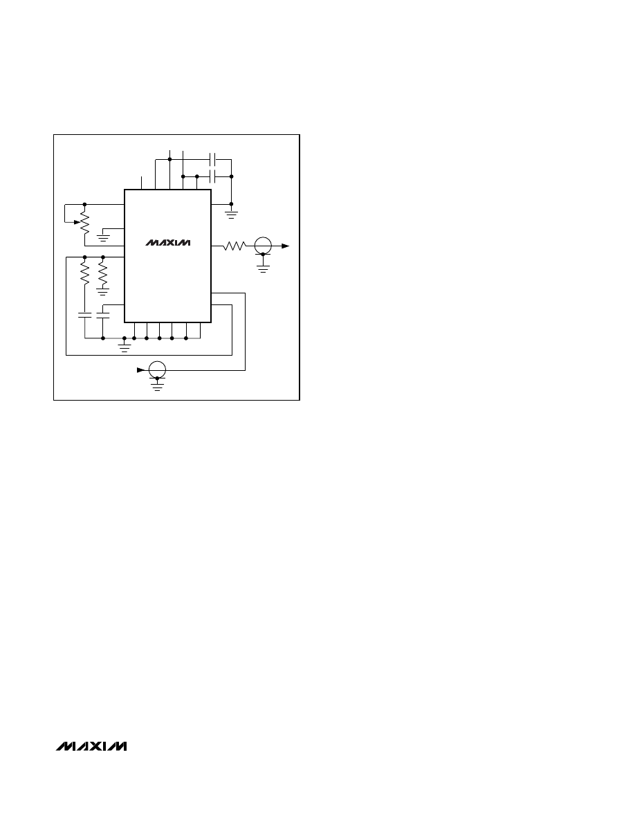
DADJ can be used to reduce the sine-wave distortion.
The unadjusted duty cycle (V
DADJ
= 0V) is 50% ±2%;
any deviation from exactly 50% causes even order har-
monics to be generated. By applying a small
adjustable voltage (typically less than ±100mV) to
V
DADJ
, exact symmetry can be attained and the distor-
tion can be minimized (see Figure 2).
The voltage on DADJ needed to produce a specific
duty cycle is given by the formula:
V
DADJ
= (50% - dc) x 0.0575
[11]
or:
V
DADJ
= (0.5 - [t
ON
÷ t
o
]) x 5.75
[12]
where:
V
DADJ
= DADJ voltage (observe the polarity)
dc = duty cycle (in %)
t
ON
= ON (positive) time
t
o
= waveform period.
Conversely, if V
DADJ
is known, the duty cycle and ON
time are given by:
dc = 50% - (V
DADJ
x 17.4)
[13]
t
ON
= t
o
x (0.5 - [V
DADJ
x 0.174])
[14]
MAX038
High-Frequency Waveform Generator
______________________________________________________________________________________
11
MAX038
1µF
GND
COSC
12
AO
V-
18
11
9
2
6
GND GND
GND GND
5
8
10
7
1
13
14
15
16
N.C.
3
FADJ
IIN
DADJ
REF
OUT
DV+
DGND
SYNC
PDI
PDO
V+ A1
4
17
20
–5V +5V
C2
1nF
C3
1µF
C1
12k
R1
20k
R
IN
FREQUENCY
50
Ω
R2
N.C.
C
F
19
SINE-WAVE
OUTPUT
2 x 2.5V
R
IN
x C
F
F
o
=
MAX038
100k
R5
5k
R6
100k
R7
100k
R3
100k
R4
DADJ
REF
+2.5V
–2.5V
PRECISION DUTY-CYCLE ADJUSTMENT CIRCUIT
ADJUST R6 FOR MINIMUM SINE-WAVE DISTORTION
Figure 2. Operating Circuit with Sine-Wave Output and 50% Duty Cycle; SYNC and FADJ Disabled

MAX038
Programming DADJ
DADJ is similar to FADJ; it has a 250µA constant cur-
rent sink to V- that must be furnished by the voltage
source. The source is usually an op-amp output, and
the temperature coefficient of the current sink becomes
unimportant. For manual adjustment of the duty cycle, a
variable resistor can be used to set V
DADJ
, but then the
250µA current sink’s temperature coefficient becomes
significant. Since external resistors cannot match the
internal temperature-coefficient curve, using external
resistors to program V
DADJ
is intended only for manual
operation, when the operator can correct for any errors.
This restriction does not apply when V
DADJ
is a true
voltage source.
A variable resistor, R
D
, connected between REF
(+2.5V) and DADJ provides a convenient means of
manually setting the duty cycle. The resistance value
(R
D
) is:
R
D
= (V
REF
- V
DADJ
) ÷ 250µA
[15]
Note that both V
REF
and V
DADJ
are signed values, so
observe correct algebraic convention. For example, if
V
DADJ
is -1.5V (23% duty cycle), the formula becomes:
R
D
= (+2.5V - (-1.5V)) ÷ 250µA
= (4.0V) ÷ 250µA = 16k
Ω
Varying the duty cycle in the range 15% to 85% has
minimal effect on the output frequency—typically less
than 2% when 25µA < I
IN
< 250µA. The DADJ circuit is
wideband, and can be modulated at up to 2MHz (see
photos,
Typical Operating Characteristics).
Output
The output amplitude is fixed at 2V
P-P
, symmetrical
around ground, for all output waveforms. OUT has an
output resistance of under 0.1
Ω
, and can drive ±20mA
with up to a 50pF load. Isolate higher output capaci-
tance from OUT with a resistor (typically 50
Ω
) or buffer
amplifier.
Reference Voltage
REF is a stable 2.50V bandgap voltage reference capa-
ble of sourcing 4mA or sinking 100µA. It is principally
used to furnish a stable current to IIN or to bias DADJ
and FADJ. It can also be used for other applications
external to the MAX038. Bypass REF with 100nF to min-
imize noise.
Selecting Resistors and Capacitors
The MAX038 produces a stable output frequency over
time and temperature, but the capacitor and resistors
that determine frequency can degrade performance if
they are not carefully chosen. Resistors should be
metal film, 1% or better. Capacitors should be chosen
for low temperature coefficient over the whole tempera-
ture range. NPO ceramics are usually satisfactory.
The voltage on COSC is a triangle wave that varies
between 0V and -1V. Polarized capacitors are generally
not recommended (because of their outrageous tem-
perature dependence and leakage currents), but if they
are used, the negative terminal should be connected to
COSC and the positive terminal to GND. Large-value
capacitors, necessary for very low frequencies, should
be chosen with care, since potentially large leakage
currents and high dielectric absorption can interfere
with the orderly charge and discharge of C
F
. If possi-
ble, for a given frequency, use lower IIN currents to
reduce the size of the capacitor.
SYNC Output
SYNC is a TTL/CMOS-compatible output that can be
used to synchronize external circuits. The SYNC output
is a square wave whose rising edge coincides with the
output rising sine or triangle wave as it crosses through
0V. When the square wave is selected, the rising edge
of SYNC occurs in the middle of the positive half of the
output square wave, effectively 90° ahead of the output.
The SYNC duty cycle is fixed at 50% and is indepen-
dent of the DADJ control.
Because SYNC is a very-high-speed TTL output, the
high-speed transient currents in DGND and DV+ can
radiate energy into the output circuit, causing a narrow
spike in the output waveform. (This spike is difficult to
see with oscilloscopes having less than 100MHz band-
width). The inductance and capacitance of IC sockets
tend to amplify this effect, so sockets are not recom-
mended when SYNC is on. SYNC is powered from sep-
arate ground and supply pins (DGND and DV+), and it
can be turned off by making DV+ open circuit. If syn-
chronization of external circuits is not used, turning off
SYNC by DV+ opening eliminates the spike.
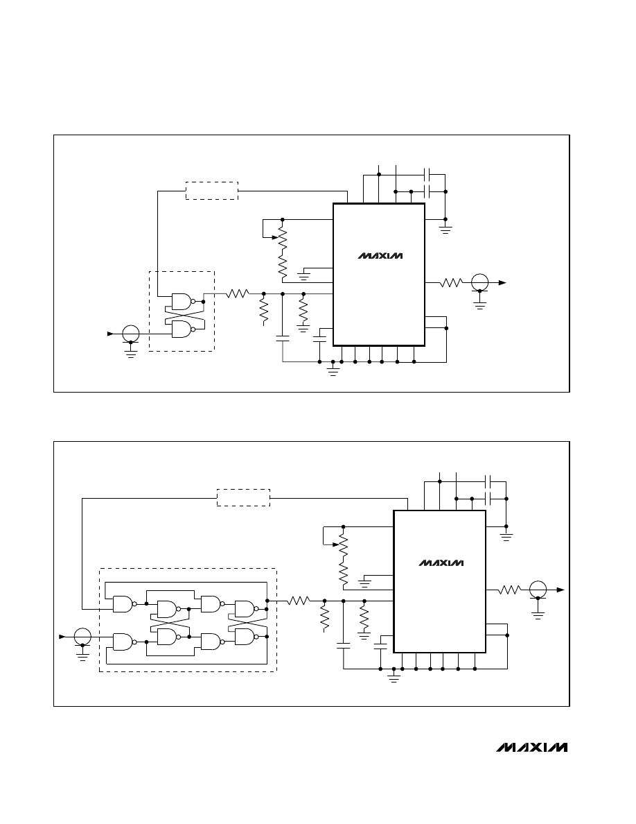
Phase Detectors
Internal Phase Detector
The MAX038 contains a TTL/CMOS phase detector that
can be used in a phase-locked loop (PLL) to synchro-
nize its output to an external signal (Figure 3). The
external source is connected to the phase-detector
input (PDI) and the phase-detector output is taken from
PDO. PDO is the output of an exclusive-OR gate, and
produces a rectangular current waveform at the
MAX038 output frequency, even with PDI grounded.
PDO is normally connected to FADJ and a resistor,
R
PD
, and a capacitor C
PD
, to GND. R
PD
sets the gain
of the phase detector, while the capacitor attenuates
high-frequency components and forms a pole in the
phase-locked loop filter.
High-Frequency Waveform Generator
12
______________________________________________________________________________________
PDO is a rectangular current-pulse train, alternating
between 0µA and 500µA. It has a 50% duty cycle when
the MAX038 output and PDI are in phase-quadrature
(90° out of phase). The duty cycle approaches 100%
as the phase difference approaches 180° and con-
versely, approaches 0% as the phase difference
approaches 0°. The gain of the phase detector (K
D
)
can be expressed as:
K
D
= 0.318 x R
PD
(volts/radian)
[16]
where R
PD
= phase-detector gain-setting resistor.
When the loop is in lock, the input signals to the phase
detector are in approximate phase quadrature, the duty
cycle is 50%, and the average current at PDO is 250µA
(the current sink of FADJ). This current is divided
between FADJ and R
PD
; 250µA always goes into FADJ
and any difference current is developed across R
PD
,
creating V
FADJ
(both polarities). For example, as the
phase difference increases, PDO duty cycle increases,
the average current increases, and the voltage on R
PD
(and V
FADJ
) becomes more positive. This in turn
decreases the oscillator frequency, reducing the phase
difference, thus maintaining phase lock. The higher
R
PD
is, the greater V
FADJ
is for a given phase differ-
ence; in other words, the greater the loop gain, the less
the capture range. The current from PDO must also
charge C
PD
, so the rate at which V
FADJ
changes (the
loop bandwidth) is inversely proportional to C
PD
.
The phase error (deviation from phase quadrature)
depends on the open-loop gain of the PLL and the ini-
tial frequency deviation of the oscillator from the exter-
nal signal source. The oscillator conversion gain (K
o
) is:
K
O
=
∆ω
o ÷
∆
VF
ADJ
[17]
which, from equation [6] is:
K
O
= 3.43 x
ω
o
(radians/sec)
[18]
The loop gain of the PLL system (K
V
) is:
K
V
= K
D
x K
O
[19]
where:
K
D
= detector gain
K
O
= oscillator gain.
With a loop filter having a response F(s), the open-loop
transfer function, T(s), is:
T(s) = K
D
x K
O
x F(s) ÷ s
[20]
Using linear feedback analysis techniques, the closed-
loop transfer characteristic, H(s), can be related to the
open-loop transfer function as follows:
H(s) = T(s) ÷ [1+ T(s)]
[21]
The transient performance and the frequency response
of the PLL depends on the choice of the filter charac-
teristic, F(s).
When the MAX038 internal phase detector is not used,
PDI and PDO should be connected to GND.
External Phase Detectors
External phase detectors may be used instead of the
internal phase detector. The external phase detector
shown in Figure 4 duplicates the action of the MAX038’s
internal phase detector, but the optional ÷N circuit can
be placed between the SYNC output and the phase
detector in applications requiring synchronizing to an
exact multiple of the external oscillator. The resistor net-
work consisting of R4, R5, and R6 sets the sync range,
while capacitor C4 sets the capture range. Note that
this type of phase detector (with or without the ÷N cir-
cuit) locks onto harmonics of the external oscillator as
well as the fundamental. With no external oscillator
input, this circuit can be unpredictable, depending on
the state of the external input DC level.
Figure 4 shows a frequency phase detector that locks
onto only the fundamental of the external oscillator.
With no external oscillator input, the output of the fre-
quency phase detector is a positive DC voltage, and
the oscillations are at the lowest frequency as set by
R4, R5, and R6.
MAX038
High-Frequency Waveform Generator
______________________________________________________________________________________
13
MAX038
GND
COSC
12
A0
V-
18
11
9
2
6
GND GND
15
DGND
GND GND
5
8
10
7
1
13
3
FADJ
IIN
DADJ
REF
R
D
OUT
PDI
PDO
V+
A1
4
17
DV+
16
20
+5V -5V
C2
1µF
C1
1µF
CENTER
FREQUENCY
50
Ω
R
OUT
C
F
R
PD
C
PD
19
RF
OUTPUT
SYNC
14
EXTERNAL OSC INPUT
Figure 3. Phase-Locked Loop Using Internal Phase Detector
MAX038
High-Frequency Waveform Generator
14
______________________________________________________________________________________
MAX038
GND
COSC
12
A0
V-
18
11
9
2
6
GND GND
15
DGND
GND GND
5
8
10
7
1
13
3
FADJ
IIN
DADJ
REF
R2
C
W
R3
OUT
PDI
PDO
V+
A1
4
17
DV+
16
20
+5V
-5V
-5V
C2
1µF
C1
1µF
CENTER
FREQUENCY
50
Ω
R1
R6
GAIN
R5
OFFSET
R4
PHASE DETECTOR
EXTERNAL
OSC INPUT
C4
CAPTURE
19
RF
OUTPUT
SYNC
14
÷N
C3
FREQUENCY
Figure 4. Phase-Locked Loop Using External Phase Detector
MAX038
GND
COSC
12
A0
V-
18
11
9
2
6
GND GND
15
DGND
GND GND
5
8
10
7
1
13
3
FADJ
IIN
DADJ
REF
R2
C
W
R3
OUT
PDI
PDO
V+
A1
4
17
DV+
16
20
+5V
-5V
-5V
C2
1µF
C1
1µF
CENTER
FREQUENCY
50
Ω
R1
R6
GAIN
R5
OFFSET
R4
C4
CAPTURE
19
RF
OUTPUT
SYNC
14
÷N
C3
FREQUENCY
EXTERNAL
OSC INPUT
FREQUENCY PHASE DETECTOR
Figure 5. Phase-Locked Loop Using External Frequency Phase Detector
MAX038
High-Frequency Waveform Generator
______________________________________________________________________________________
15
N4
N3
N2
MC145151
N6
8.192MHz
MAX427
N5
OUT1
OUT2
RFB
VREF
VDD
GND1
MX7541
N7
N8
N9
T/R
N12
N13
N10
N11
OSC
OUT
OSC
IN
LD
N
N1
N0
FV
PDV
PDR
RA2
RA1
RA0
PD1
OUT
V
DD
V
SS
F
IN
35pF
20pF
15
14
28
1
GND
BIT1
BIT2
BIT3
BIT4
BIT5
BIT6
BIT12
BIT11
BIT10
BIT9
BIT8
BIT7
MAX038
A0
A1
COSC
GND1
DADJ
FADJ
OUT
GND
V+
DV+
DGND
SYNC
PDI
PDO
VREF
V-
GND1
IIN
GND1
3.3M
PDV
PDR
3.3M
33k
0.1
µ
F
0.1
µ
F
33k
0.1
µ
F
0.1
µ
F
7.5k
10k
2
3
7
4
6
0.1
µ
F
0.1
µ
F
+2.5V
±2.5V
35
pF
10
11
0.1
µ
F
0.1
µ
F
0.1
µ
F
50.0
100
1
20
50
Ω
, 50MHz
LOWPASS FILTER
220nH
220nH
56pF
110pF
56pF
50
Ω
SIGNAL
OUTPUT
SYNC
OUTPUT
+5V
-5V
9
10
1
18
3
2
1
0V TO 2.5V
2N3904
3.33k
2.7M
1k
1k
5
6
8
4
7
2N3906
1N914
2
µ
A to
750
µ
A
MAX412
MAX412
8.192MHz
4.096MHz
2.048MHz
1.024MHz
512kHz
256kHz
128kHz
64kHz
32kHz
16kHz
8kHz
4kHz
2kHz
1kHz
WAVEFORM
SELECT
FREQUENCY SYNTHESIZER 1kHz RESOLUTION; 8kHz TO 16.383MHz
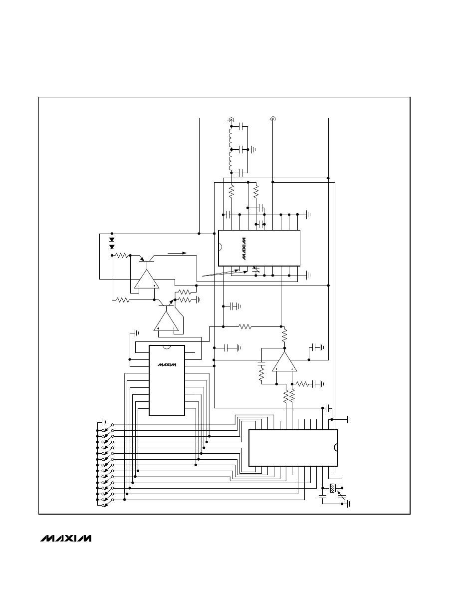
Figure 6. Crystal-Controlled, Digitally Programmed Frequency Synthesizer—8kHz to 16MHz with 1kHz Resolution
MAX038
High-Frequency Waveform Generator
16
______________________________________________________________________________________
Layout Considerations
Realizing the full performance of the MAX038 requires
careful attention to power-supply bypassing and board
layout. Use a low-impedance ground plane, and con-
nect all five GND pins directly to it. Bypass V+ and V-
directly to the ground plane with 1µF ceramic capaci-
tors or 1µF tantalum capacitors in parallel with 1nF
ceramics. Keep capacitor leads short (especially with
the 1nF ceramics) to minimize series inductance.
If SYNC is used, DV+ must be connected to V+, DGND
must be connected to the ground plane, and a second
1nF ceramic should be connected as close as possible
between DV+ and DGND (pins 16 and 15). It is not
necessary to use a separate supply or run separate
traces to DV+. If SYNC is disabled, leave DV+ open.
Do not open DGND.
Minimize the trace area around COSC (and the ground
plane area under COSC) to reduce parasitic capaci-
tance, and surround this trace with ground to prevent
coupling with other signals. Take similar precautions
with DADJ, FADJ, and IIN. Place C
F
so its connection
to the ground plane is close to pin 6 (GND).
__________Applications Information
Frequency Synthesizer
Figure 6 shows a frequency synthesizer that produces
accurate and stable sine, square, or triangle waves with
a frequency range of 8kHz to 16.383MHz in 1kHz incre-
ments. A Motorola MC145151 provides the crystal-con-
trolled oscillator, the ÷N circuit, and a high-speed phase
detector. The manual switches set the output frequency;
opening any switch increases the output frequency.
Each switch controls both the ÷N output and an
MX7541 12-bit DAC, whose output is converted to a cur-
rent by using both halves of the MAX412 op amp. This
current goes to the MAX038 IIN pin, setting its coarse
frequency over a very wide range.
Fine frequency control (and phase lock) is achieved
from the MC145151 phase detector through the differ-
ential amplifier and lowpass filter, U5. The phase detec-
tor compares the ÷N output with the MAX038 SYNC
output and sends differential phase information to U5.
U5’s single-ended output is summed with an offset into
the FADJ input. (Using the DAC and the IIN pin for
coarse frequency control allows the FADJ pin to have
very fine control with reasonably fast response to switch
changes.)
A 50MHz, 50
Ω
lowpass filter in the output allows pas-
sage of 16MHz square waves and triangle waves with
reasonable fidelity, while stopping high-frequency noise
generated by the ÷N circuit.
V+
PDI
SYNC
AO
DADJ
PDO
FADJ
0.118"
(2.997mm)
0.106"
(2.692mm)
A1
COSC
GND
IIN
GND
GND
DGND
DV+
GND
GND
REF
V-
OUT
TRANSISTOR COUNT: 855
SUBSTRATE CONNECTED TO GND
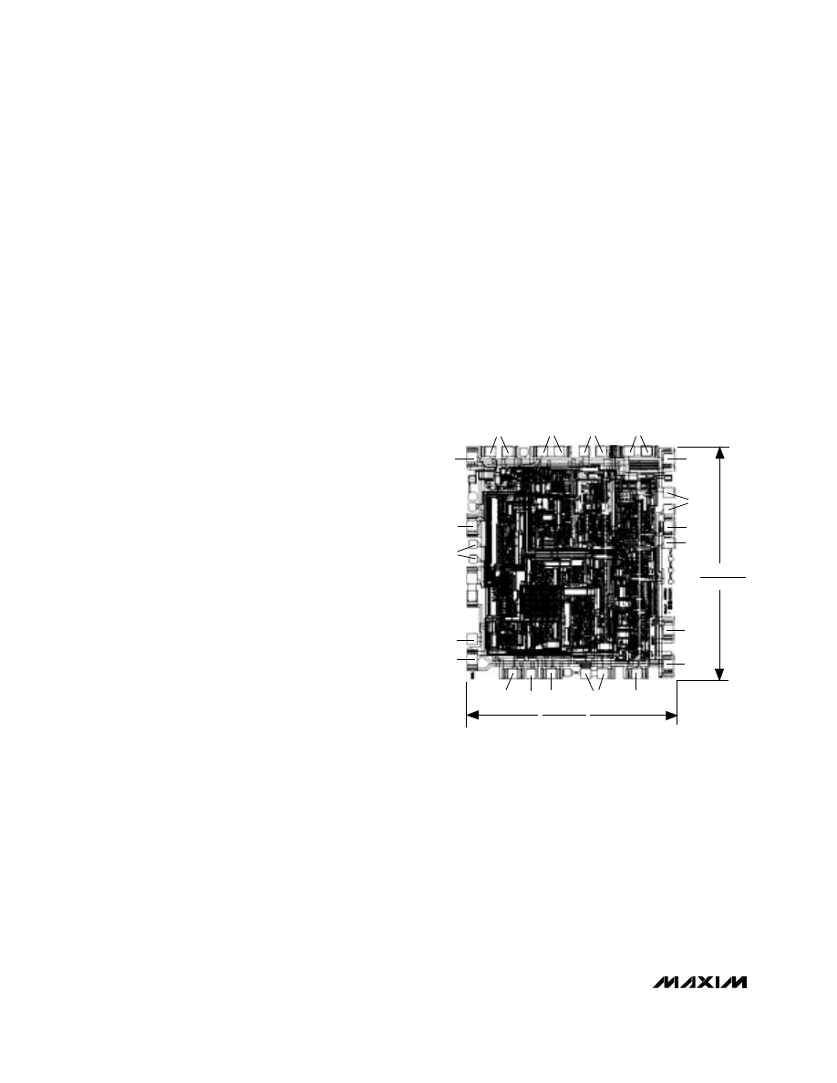
___________________Chip Topography
Wyszukiwarka
Podobne podstrony:
MAX038 kit
MAX038 Gen
MAX038
MAX038, Przedstawiony w artykule generator mo?e zadowoli? nawet zaawansowanych amator?w
max038xx
MAX038 kit
więcej podobnych podstron