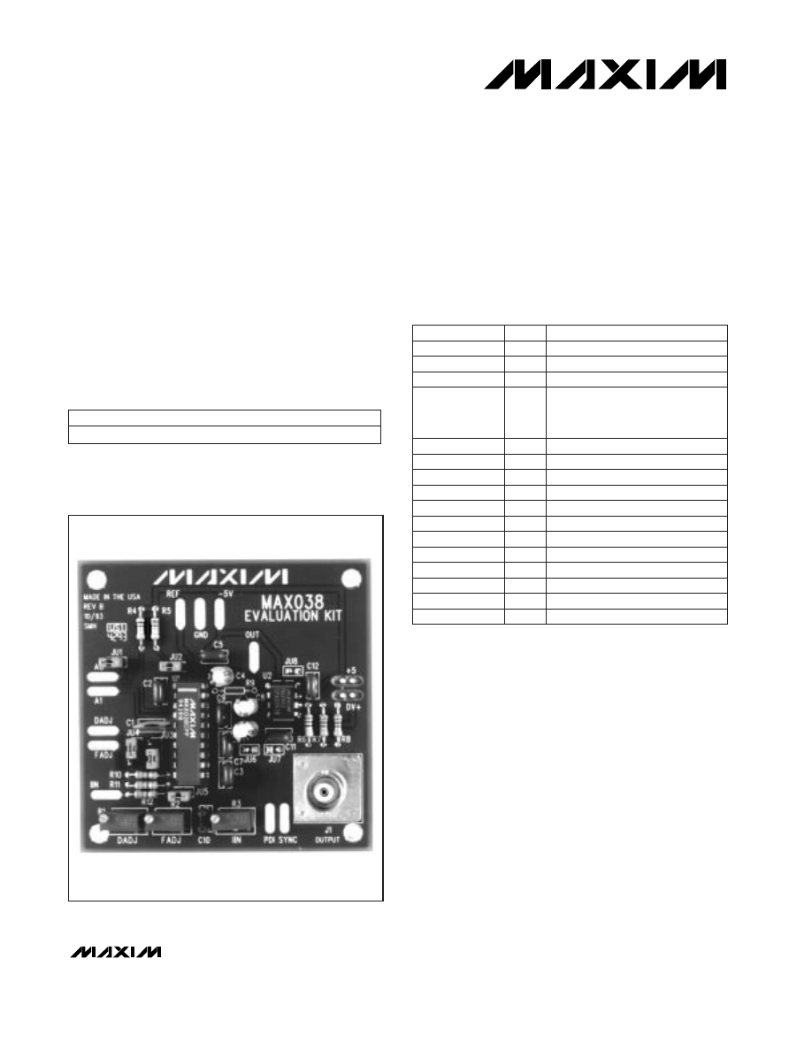
Evaluates: MAX038
MAX038 Evaluation Kit
________________________________________________________________ Maxim Integrated Products
1
_______________General Description
The MAX038 evaluation kit (EV kit) is a high-frequency
function generator capable of producing accurate tri-
angle/sawtooth, sine, and square/pulse waveforms up
to 10MHz, using the supplied components. Output fre-
quency and duty cycle are easily adjusted with on-
board potentiometers. Removable jumpers select sine,
square, or triangle waveforms, or fix the duty cycle at
50%. The output is buffered with a MAX442 amplifier
capable of driving a 50
Ω
coaxial cable. The MAX038
EV kit is fully assembled and tested.
___________________________Features
♦
325kHz to 10MHz Operation
♦
Adjustable Duty Cycle
♦
2.5V Reference Output
♦
TTL-Compatible SYNC Output
♦
Fully Assembled and Tested
____________________Component List
_________________________Quick Start
The MAX038 EV kit is a fully assembled and tested
board. Follow these steps to verify board operation.
Do
not turn on the power supply until all connections
are completed.
1) Connect a +5V supply to the pad marked +5V.
Connect a -5V supply to the pad marked -5V.
Connect ground(s) to the GND pad.
2) Connect an oscilloscope to the BNC jack marked
OUTPUT through a terminated 50
Ω
cable. The
MAX038 output prior to the amplifier stage may also
be monitored using an oscilloscope probe at the
OUT pad.
3) Place the shunt across pins 2 and 3 of JU4 for 50%
duty cycle. Place the shunt across pins 1 and 2 of
______________Ordering Information
______________________________EV Kit
DESIGNATION
QTY
DESCRIPTION
U1
1
MAX038CPP
U2
1
MAX442CPA
C1
1
82pF capacitor
C2, C3, C5, C7,
C9, C10, C11,
C12
8
0.1µF capacitors
C4, C6, C8
3
4.7µF capacitors
R1, R2
2
20k
Ω
potentiometers
R3
1
50k
Ω
potentiometer
R4, R5
2
10k
Ω
, 5% resistors
R6
1
51
Ω
, 5% resistor
R7, R8
2
270
Ω
, 5% resistors
R9, R10, R11
3
0
Ω
resistors
R12
1
3.3k
Ω
, 5% resistor
JU1, JU2, JU5
3
2-pin headers
JU3, JU4
2
3-pin headers
None
5
Shunts
J1
1
BNC jack
PART
MAX038EVKIT-DIP
0°C to +70°C
TEMP. RANGE
BOARD TYPE
Through-Hole
For free samples & the latest literature: http://www.maxim-ic.com, or phone 1-800-998-8800.
For small orders, phone 408-737-7600 ext. 3468.
JU3 to allow the frequency to be adjusted. Verify
that there is a shunt on JU5.
4) Verify the shunts on JU1 and JU2 for a square-wave
output. Refer to Table 1 for alternate waveform
selections.
5) Apply power and verify the output waveform.
_______________Detailed Description
Waveform Selection
To select the desired output waveform, place shunts
across JU1 and JU2 in the combinations shown in
Table 1. These jumpers set address pins A0 and A1 to
TTL/CMOS-logic levels. External control may be initiat-
ed by connecting an external source to the A0 and
A1 pads and removing the shunts on JU1 and JU2.
Note that there are 10k
Ω
pull-up resistors to +5V on the
A0 and A1 address lines.
* Note: Frequency pre-set by oscillator capacitor (C1) and input
current (position of R3) as specified by formula [1].
Output Frequency
The output frequency is controlled by the oscillator
capacitor (C1), the current injected into the IIN pin, and
the voltage on the FADJ pin. The EV kit allows indepen-
dent adjustment of both input current (R3) and FADJ
voltage (R2). Refer to the
Detailed Description section
of the MAX038 data sheet for additional theory of oper-
ation.
Input Current Control
The current injected into the IIN pin acts as the primary
frequency-adjustment control. The R3 potentiometer
varies the current to the MAX038’s IIN pin. The input
current can be easily monitored by removing the JU5
shunt and placing a current meter across the JU5 pins.
The components supplied on the EV kit will allow an
input current range of 50µA to 725µA. With the VADJ
pin grounded, the fundamental output frequency (F
o
) is
as follows:
F
o
(MHz) = I
IN
(µA)
÷
C
OSC
(pF) [1]
where: I
IN
= current injected into IIN
= V
REF
÷
(R3 + R12)
= 2.5V
÷
(0k
Ω
to 50k
Ω
+ 3.3k
Ω
)
C
OSC
= external oscillator capacitor (C1)
To use an external input current, connect the external
current source to the IIN pad and remove the JU5 shunt
completely. Note that there is a 3.3k
Ω
resistor in series
with the device IIN pin.
FADJ Control
Varying the FADJ voltage will also vary the output fre-
quency. With a shunt across pins 1 and 2 of JU3, the
R2 potentiometer will vary the voltage applied to the
FADJ pin. With the JU3 shunt on pins 2 and 3, the FADJ
pin is grounded. Grounding the FADJ pin sets the out-
put to the fundamental output frequency (F
o
), as
given by equation [1].
To use an external FADJ voltage, connect the external
source to the FADJ pad and remove the JU3 shunt
completely. Limit the external FADJ voltage to ±2.4V.
Duty-Cycle Control
The voltage on the DADJ pin controls the duty cycle of
the output waveform. With the JU4 shunt on pins 1 and 2,
the R1 potentiometer will vary the voltage applied to the
DADJ pin, thus varying the duty cycle 15% to 85%. With
the JU4 shunt on pins 2 and 3, the DADJ pin is grounded.
Grounding the DADJ pin fixes the duty cycle at 50%.
To use an external DADJ voltage, connect the external
voltage source to the DADJ pad and remove the JU4
shunt completely. Limit the external DADJ voltage to
±2.3V.
Evaluates: MAX038
MAX038 Evaluation Kit
2
_______________________________________________________________________________________
Table 1. Waveform Jumper Select
Table 2. Frequency and Duty-Cycle Jumper Select
Fixed 50% Duty Cycle
2 & 3
JU4
Adjustable Duty Cycle
1 & 2
Pre-Set Frequency*
2 & 3
JU3
Adjustable Frequency
1 & 2
MAX038 OUTPUT
SHUNT
LOCATION
JUMPER
Square Wave
Short
Short
Triangle Wave
Short
Open
Sine Wave
Open
Don't Care
OUTPUT WAVEFORM
JU2
JU1

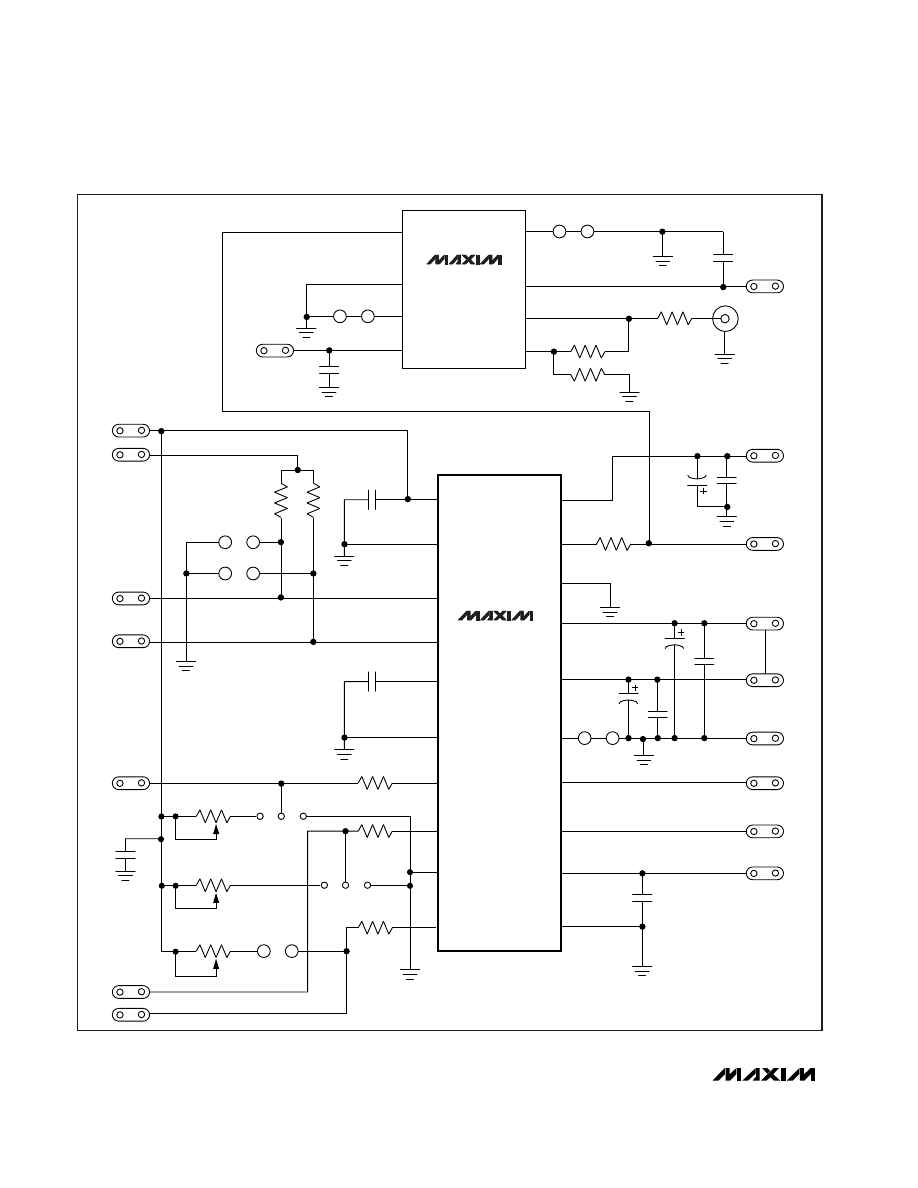
Output Buffer
The MAX038 output amplitude is fixed at 2V
p-p
. The
MAX038 output is capable of driving a capacitive load
up to 90pF. The MAX442 amplifier buffers the MAX038
output to a 50
Ω
coaxial cable. The MAX442 is set at a
gain of 2V/V, so that the output amplitude remains 1V/V
after the 50
Ω
back termination. The EV kit’s OUT pad
provides access to the output of the MAX038 prior to
the MAX442 buffer stage. The MAX442 output connects
to the BNC connector through a 50
Ω
resistor to back
terminate a 50
Ω
coaxial cable. When a terminated 50
Ω
cable is connected, this resistor forms a voltage divider
with the load impedance, which attenuates the signal
by one-half. The MAX442 is operated with a 2V/V
closed-loop gain to provide unity gain at the 50
Ω
cable’s output.
The MAX442 is actually a 2-channel amplifier. A built-
in multiplexer allows either of two input signals to be
selected. TTL-level address pin A0 selects either IN0
or IN1. The MAX038 output is connected to MAX442
input IN0. IN1 is unused and connected to ground; it
may be used by cutting the JU7 trace, thus discon-
necting IN1 from ground. Likewise, the MAX442
address pin A0 can be disconnected from ground by
cutting the JU8 trace. Pull up A0 to +5V to select IN1.
See the MAX442 data sheet for additional operation
details.
Reference Voltage
The MAX038 includes a 2.5V bandgap reference capa-
ble of sourcing 4mA and sinking 100µA. Access to the
reference voltage is provided at the REF pad. The ref-
erence voltage is primarily used to provide stable cur-
rent to IIN and to bias DADJ and FADJ.
Extending the Output
Frequency Range
The components supplied with the EV kit allow an out-
put frequency range of 325kHz to 10MHz. The frequen-
cy range is controlled primarily by the oscillator capaci-
tor (C1) and the input current, which is a function of the
reference voltage and potentiometer R3. The resulting
frequency range can be shifted up or down depending
on the value of C1. Refer to the Output Frequency vs.
Input Current graph which appears in the
Typical
Operating Characteristics of the MAX038 data sheet.
The upper end of the range can be extended by reduc-
ing C1. The lower end of the range can be reduced by
increasing the value of C1. Take care when selecting
alternate capacitors if stable operation over tempera-
ture is desired. Ceramic capacitors with low tempera-
ture coefficients give the best results. Refer to the
Selecting Resistors and Capacitors section of the
MAX038 data sheet for further details.
Sync Output
and Phase-Detector Input
Refer to the
SYNC Output and Phase Detector sections
of the MAX038 data sheet for details of circuit synchro-
nization. Access to the Phase Detector Input (PDI) and
SYNC is provided at pads PDI and SYNC.
High-speed transient currents in DGND and DV+ can
cause a switching spike in the output waveform at the
zero-crossing point. A lowpass output filter, as shown in
Figure 3 of the MAX038 data sheet, may be used to
greatly reduce the spike. Complete LC filter assemblies
(S3LP series) are available from Coilcraft (phone:
708-639-6400). If the SYNC output is not required, dis-
abling the SYNC circuit will eliminate the switching
spike. Cut the trace between the DV+ and +5V pads to
disable the SYNC output.
Evaluates: MAX038
MAX038 Evaluation Kit
_______________________________________________________________________________________
3
Evaluates: MAX038
MAX038 Evaluation Kit
4
_______________________________________________________________________________________
MAX038
U1
GND
REF
A1
A0
GND
COSC
FADJ
DADJ
IIN
FADJ
DADJ
A1
A0
+5V
REF
IIN
3
2
1
GND
OUT
V-
V+
GND
MAX442
U2
GND
IN0
IN1
V+
A0
VOUT
V-
7
8
6
5
C11
0.1
µ
F
R9
0
Ω
R10
0
Ω
R11
0
Ω
R2
20k
R3
50k
R1
20k
R12
3.3k
C12
0.1
µ
F
C5
0.1
µ
F
C9
0.1
µ
F
C3
0.1
µ
F
C7
0.1
µ
F
C4
4.7
µ
F
C6
4.7
µ
F
C8
4.7
µ
F
C2
0.1
µ
F
C1
82pF
2
1
3
4
-5V
IN-
DGND
DV+
PDI
SYNC
GND
PDO
2
1
4
3
6
5
8
7
10
9
19
20
17
18
15
16
13
14
11
12
PDO
PDI
SYNC
GND
+5V
DV+
OUT
–5V
+5V
JU8
CUT HERE
JU7
CUT HERE
JU6
CUT HERE
JU1
JU2
JU5
JU4
JU3
R7
270
Ω
R4
10k
R5
10k
R8
270
Ω
R6
51
Ω
J1
BNC
OUTPUT
3
2
1
C10
0.1
µ
F
CUT HERE
TO DISABLE
SYNC
Figure 1. MAX038 EV Kit Schematic
Evaluates: MAX038
MAX038 Evaluation Kit
_______________________________________________________________________________________
5
Figure 2. MAX038 EV Kit Component Placement Guide—Component Side
Evaluates: MAX038
MAX038 Evaluation Kit
6
_______________________________________________________________________________________
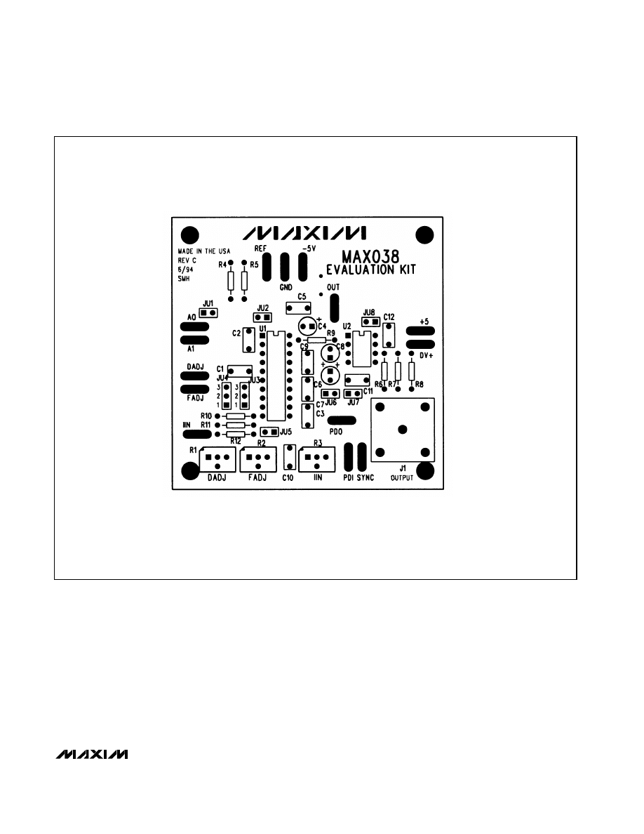
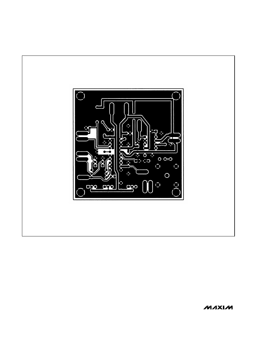
Figure 3. MAX038 EV Kit PC Board Layout—Component Side
Evaluates: MAX038
MAX038 Evaluation Kit
_______________________________________________________________________________________
7
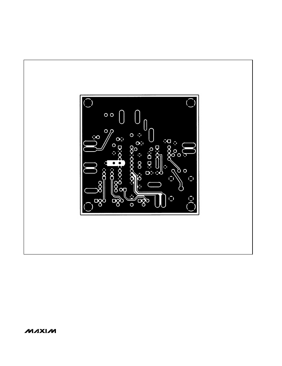
Figure 4. MAX038 EV Kit PC Board Layout—Solder Side

Evaluates: MAX038
MAX038 Evaluation Kit
NOTES
Maxim cannot assume responsibility for use of any circuitry other than circuitry entirely embodied in a Maxim product. No circuit patent licenses are
implied. Maxim reserves the right to change the circuitry and specifications without notice at any time.
8
_____________________Maxim Integrated Products, 120 San Gabriel Drive, Sunnyvale, CA 94086 408-737-7600
© 1996 Maxim Integrated Products
Printed USA
is a registered trademark of Maxim Integrated Products.
Wyszukiwarka
Podobne podstrony:
Media kit IRE PL
KIT EKG01 pl
KiT wykład 7
KIT, interna
KIT WYKŁAD 2
GeneJET genomic DNA purification kit (cw2)
MPC The Kit Owners Manual
Ets Toefl Preparation Kit Volume 2 Practice Test C Rc
Drum Kit Lessons Double Paradiddle As Drum Kit Beats
MAX038
MI KIT NANO SERVICE CLIMA pl PL DEX01
Anti Hacker Tool Kit Edycja polska
22 Minute Hard Corps Calendar Base Kit
family kit instructions
kit
MAX038 Gen
Opis płyty ADSP 21065L EZ KIT Lite Manual Rev2
więcej podobnych podstron