
Professional Radio
GP Series
Lowband (29.7-42MHz and 35-50MHz)
Service Information
Issue: June 2002

ii
Computer Software Copyrights
The Motorola products described in this manual may include copyrighted Motorola computer programs stored
in semiconductor memories or other media. Laws in the United States and other countries preserve for
Motorola certain exclusive rights for copyrighted computer programs, including the exclusive right to copy or
reproduce in any form, the copyrighted computer program. Accordingly, any copyrighted Motorola computer
programs contained in the Motorola products described in this manual may not be copied or reproduced in
any manner without the express written permission of Motorola. Furthermore, the purchase of Motorola
products shall not be deemed to grant, either directly or by implication, estoppel or otherwise, any license
under the copyrights, patents or patent applications of Motorola, except for the normal non-exclusive royalty-
free license to use that arises by operation of law in the sale of a product.

iii
Table of Contents
Chapter 1
MODEL CHART AND TECHNICAL SPECIFICATIONS
1.0 GP340/GP380 Model Chart .................................................................................1-1
2.0 Technical Specifications ......................................................................................1-2
Chapter 2
THEORY OF OPERATION
1.0 Lowband Transmitter ...........................................................................................2-1
1.1 Power Amplifier (PA) ......................................................................................2-1
1.2 Antenna Switch...............................................................................................2-2
1.3 Harmonic Filter ...............................................................................................2-2
1.4 Antenna Matching Network ............................................................................2-2
1.5 Power Control Integrated Circuit (PCIC) ........................................................2-2
1.6 Temperature Cut Back Circuit ........................................................................2-2
2.0 Lowband Receiver ...............................................................................................2-3
2.1 Receiver Front-End ........................................................................................2-3
2.2 Receiver Back-End.........................................................................................2-4
2.3 Automatic Gain Control (AGC) .......................................................................2-5
2.4 Frequency Generation Circuit.........................................................................2-5
3.0 Synthesizer ..........................................................................................................2-6
4.0 Voltage Control Oscillator (VCO) .........................................................................2-7
4.1 Receive VCO..................................................................................................2-7
4.2 Transmit VCO.................................................................................................2-7
4.3 Buffer ..............................................................................................................2-7
4.4 Diplexer and Output Filters.............................................................................2-7
4.5 Prescalar Feedback........................................................................................2-7
Chapter 3
TROUBLESHOOTING CHARTS
1.0 Receiver (Sheet 1 of 2) ........................................................................................3-1
2.0 Receiver (Sheet 2 of 2) ........................................................................................3-2
3.0 Transmitter...........................................................................................................3-3
4.0 Synthesizer ..........................................................................................................3-4
5.0 Voltage Controlled Oscillator ...............................................................................3-5
Chapter 4
LOWBAND SCHEMATICS
1.0 Allocation of Schematics and Circuit Boards .......................................................4-1
1.1 Controller Circuits ...........................................................................................4-1
2.0 Schematics ..........................................................................................................4-3
3.0 Parts List ............................................................................................................4-12

iv
Chapter 1
MODEL CHART AND TECHNICAL SPECIFICATIONS
1.0
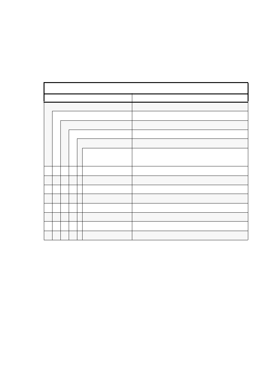
GP340 / GP380 Model Chart
Professional GP300 Series (LB)
Model
Description
MDH25BEC9AN3_E
GP340 LB1 29.7-42 MHz 6W 16-Ch
MDH25BEH9AN6_E
GP380 LB1 29.7-42 MHz 6W 255-Ch
MDH25CEC9AN3_E
GP340 LB2 35-50 MHz 6W 16-Ch
MDH25CEH9AN6_E
GP380 LB2 35-50 MHz 6W 255-Ch
Item
Description
X
PMLB4006_
GP340 LB1 Back Cover Kit
X
PMLB4016_
GP380 LB1 Back Cover Kit
X
PMLB4012_
GP340 LB2 Back Cover Kit
X
PMLB4017_
GP380 LB2 Back Cover Kit
X
X
6864110B13
GP340 Basic User Guide
X
X
6864110B18
GP380 Basic User Guide
X
X
X
X
NAB6064_
Low/Mid Band (29-50MHz) Heliflex, Trimmable Antenna
X
X
X
X
HNN9008_
Battery, NiMH Standard
x = Indicates one of each is required.
1-2
MODEL CHART AND TECHNICAL SPECIFICATIONS
2.0
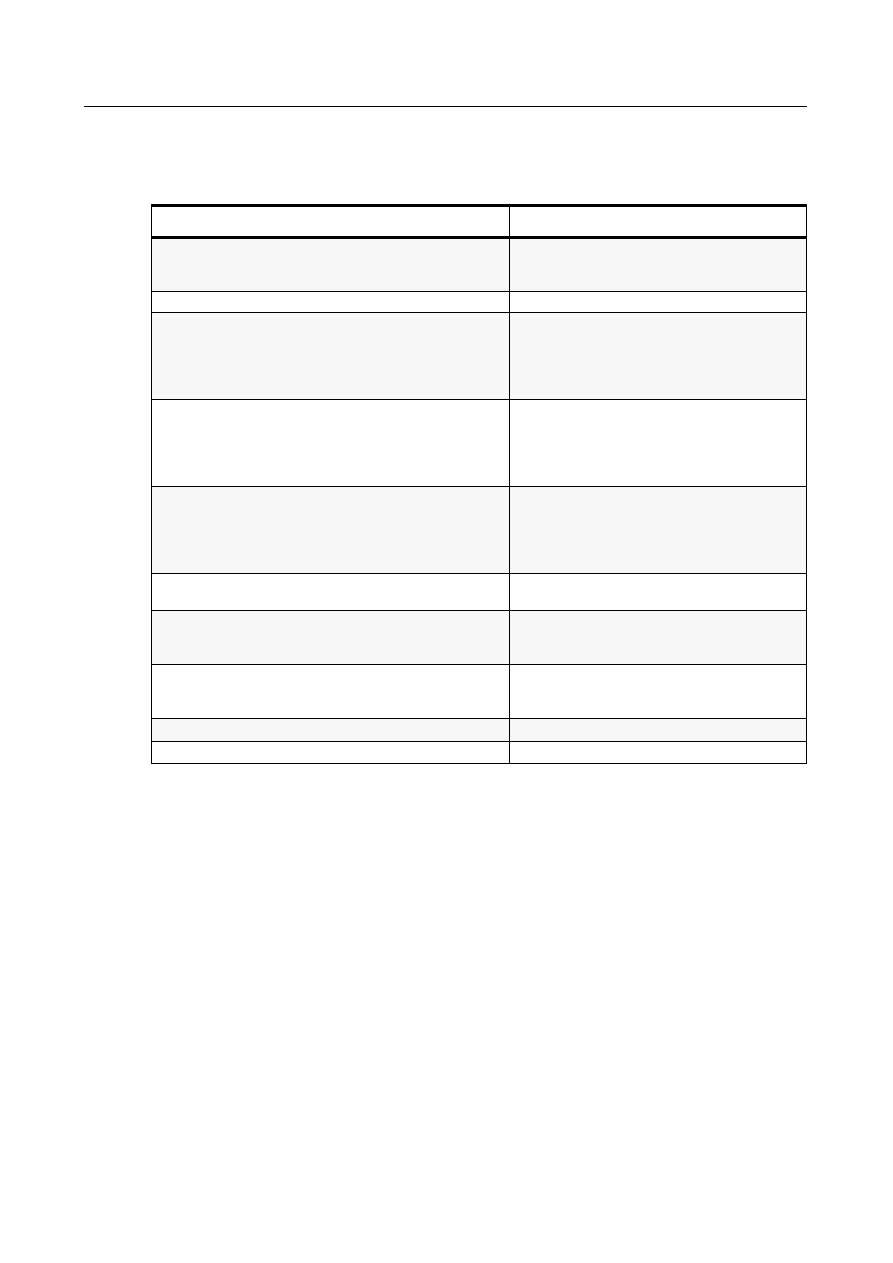
Technical Specifications
Data is specified for +25°C unless otherwise stated.
General Specifications
Channel Capacity
GP340
GP380
16
255
Power Supply
Rechargeable battery 7.5v
Dimensions: H x W x D (mm)
With standard high capacity NiMH battery
With ultra high capacity NiMH battery
With NiCD battery
With Lilon battery
Height excluding knobs
137 x 57.5 x 37.5
137 x 57.5 x 40.0
137 x 57.5 x 40.0
137 x 57.5 x 33.0
Weight: (gm)
With Standard high capacity NiMH battery
With Ultra high capacity NiMH battery
With NiCD battery
With Lilon battery
GP340
GP380
420
428
500
508
450
458
350
358
Average Battery Life @5/5/90 Cycle:
With Standard high capacity NiMH battery
With Ultra high capacity NiMH battery
With NiCD battery
With Lilon battery
Low Power
High Power
11 hours
8 hours
14 hours
11 hours
12 hours
9 hours
11 hours
8 hours
Sealing:
Withstands rain testing per
MIL STD 810 C/D /E and IP54
Shock and Vibration:
Protection provided via impact
resistant housing exceeding MIL STD
810-C/D /E and TIA/EIA 603
Dust and Humidity:
Protection provided via environment
resistant housing exceeding MIL STD
810 C/D /E and TIA/EIA 603
Technical Specifications
1-3
*Availability subject to the laws and regulations of individual countries.
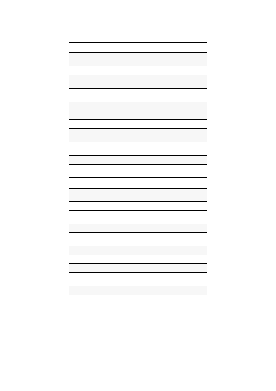
Transmitter
LB
*Frequencies - Full Bandsplit
LB1 29.7-42 MHz
LB2 35-50 MHz
Channel Spacing
12.5/20/25 kHz
Frequency Stability
(-25°C to +55°C, +25° Ref.)
±10ppm
Power
1-6W
Modulation Limiting
±2.5 @ 12.5 kHz
±4.0 @ 20 kHz
±5.0 @ 25 kHz
FM Hum & Noise
-40 dB typical
Conducted/Radiated Emission
-36 dBm <1 GHz
-30 dBm >1 GHz
Adjacent Channel Power
-60 dB @ 12.5 kHz
-70 dB @ 25 kHz
Audio Response (300 - 3000 Hz)
+1 to -3 dB
Audio Distortion
<3% typical
Receiver
LB
*Frequencies - Full Bandsplit
LB1 29.7-42 MHz
LB2 35-50 MHz
Channel Spacing
12.5/20/25 kHz
Sensitivity (12 dB SINAD) EIA
Sensitivity (20 dB SINAD) ETS
0.25 µV typical
0.50 µV typical
Intermodulation EIA
65 dB
Adjacent Channel Selectivity
60 dB @ 12.5 kHz
70 dB @ 25 kHz
Spurious Rejection
>70 dB
Rated Audio
0.5W
Audio Distortion @ Rated Audio
<3% typical
Hum & Noise
-45 dB @ 12.5 kHz
-50 dB @ 20/25 kHz
Audio Response (300 - 3000 Hz)
+1 to -3 dB
Conducted Spurious Emission
-57 dBm <1 GHz
-47 dBm >1 GHz
ETS 300 086

1-4
MODEL CHART AND TECHNICAL SPECIFICATIONS
Chapter 2
THEORY OF OPERATION
1.0
Introduction
This chapter provides a detailed theory of operation for the radio RF circuits. Refer to the relevant
section of this manual for details of the operation of the Controller Circuits.
2.0
Lowband Transmitter
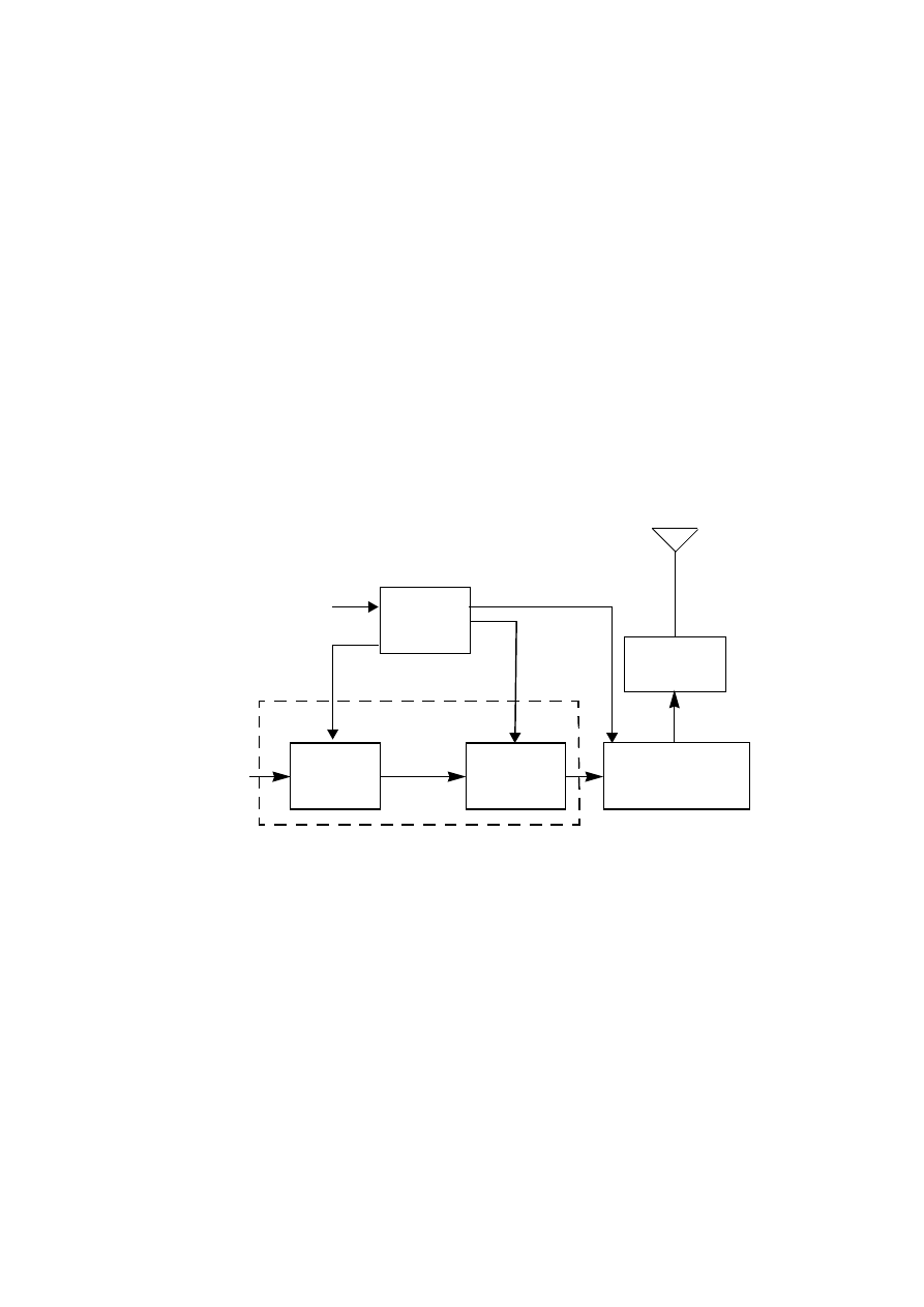
(Refer to Figure 2-1 and the Lowband Transmitter schematic diagram)
The Lowband transmitter consists of the following basic circuits :
■
Power amplifier (PA).
■
Antenna switch/harmonic filter.
■
Antenna matching network.
■
Power Control Integrated Circuit (PCIC).
Figure 2-1 Lowband Transmitter Block Diagram.
2.1
Power Amplifier (PA)
The power amplifier (PA) consists of two LDMOS devices:
1.
PA driver IC, U101.
2.
PA final stage, Q100.
The LDMOS driver (U101) provides 2-stage amplification using a supply voltage of 7.3V. The
amplifier is capable of supplying an output power of 0.3W (pins 6 and 7) with an input signal of 2mW
at (pin16). The current drain is typically 120mA while operating in the frequency range of
29.7 - 50 MHz. The power output of this stage is varied by the power control loop which controls the
voltage on pin 1.
P C I C
SPI Bus
Antenna switch bias
V Control
Power Amplifier (PA)
PA Driver
PA Final
Stage
Antenna Switch/
Harmonic Filter
Antenna
Matching
Network
Gate bias

2-2
THEORY OF OPERATION
The LDMOS PA is capable of supplying an output power of 8W with an input signal of 0.3W. The
current drain is typically 2000 mA while operating in the frequency range of 29.7 - 50 MHz. The final
stage gate is bias by a voltage from PCIC pin 24. This voltage is the output of a programmable DAC
inside the PCIC and the output is adjustable with the radio tuner.
2.2
Antenna Switch
The antenna switch circuit consists of two pin diodes (D100 and D101), a RF network (C147 and
L103), and a DC feed network (L104, C144 and current limiting resistor R101). In the transmit
mode, PCIC (U102) pin 32 goes high supplying current via the feed network to bias the diodes “on”.
The shunt diode (D101) shorts out the receiver port and L103 is connected from the RF path to
ground. L103 and the input capacitance of the lowpass filter form a parallel resonant circuit,
effectively disconnecting the receiver port from the antenna while not loading the transmit path. In
the receive mode, pin 32 goes low and the diodes are off. D100 looks like a high impedance
disconnecting the transmitter from the antenna while L103 and C147 form a series resonant circuit
to connect the receiver to the antenna.
2.3
Harmonic Filter
The harmonic filter consists of components C103, C106, C107, C110, C111, C114, C115 and
inductors L100, L101 and L102, which are a part of the SH100 assembly. The harmonic filter for
lowband is pole zero design which gives greater attenuation in low frequencies where the harmonic
energy of the transmitter is the greatest and less attenuation in high frequencies where there is less
harmonic energy. The harmonic filter insertion loss is typically less than 0.8 dB.
2.4
Antenna Matching Network
The antenna matching network (T100) matches the antenna impedance with the harmonic filter to
optimize the performance of the transmitter and receiver.
2.5
Power Control Integrated Circuit (PCIC)
The transmitter uses the PCIC (U102) to regulate the power output of the radio. To accomplish this,
the voltage across R102 is sensed. This voltage drop is directly proportional to the current drawn in
the final stage of the transmitter. This voltage is compared to a programmable reference inside the
PCIC and the voltage on PCIC pin 4 adjusted. Pin 4 connects to the PA driver IC (U101) pin 1 via
resistor R100 and varies RF output power of the driver. This controls the current drain of the final
stage and sets the output power.
2.6
Temperature Cut Back Circuit
Temperature sensor VR101 and associated components are part of a temperature cut back circuit.
This circuit senses the printed circuit board temperature around the transmitter circuits and outputs
a DC voltage to the PCIC. If the DC voltage produced exceeds the set threshold of the PCIC, the
transmitter output power decreases to reduce the transmitter temperature.
Lowband Receiver
2-3
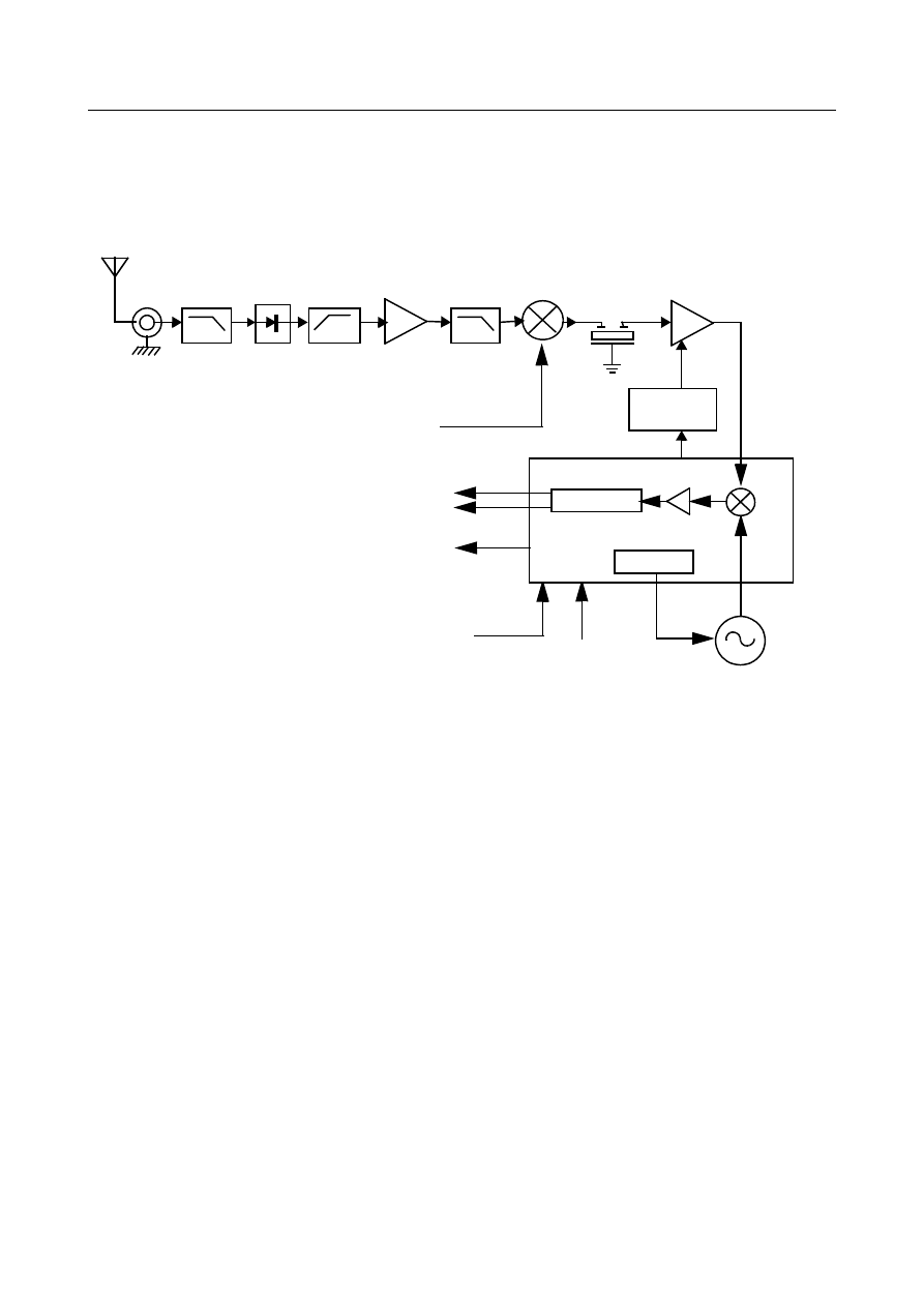
3.0
Lowband Receiver
(Refer to Figure 2-2 and the Receiver Front End and Receiver Back End schematic diagrams)
The Lowband receiver consists of a front end, back end, and automatic gain control circuits.
Detailed descriptions of these stages are contained in the paragraphs that follow.
Figure 2-2 Lowband Receiver Block Diagram.
3.1
Receiver Front-End
(Refer to the Receiver Front End, Receiver Back end and Transmitter schematic diagrams)
The RF signal received by the antenna is routed through the transmitter lowpass filter and antenna
switch. These circuits are described in the transmitter section.The signal next passes through a
highpass filter consisting of L501, L502, C538, C533 and C504. This filter serves to reject below
band signals and has a 3 dB corner frequency of 27 MHz.
The output of the highpass filter is connected to an RF amp consisting of Q509 and associated
biasing components. This is a BJT amplifier powered off 5 volts and has 13 dB of gain. The amplifier
drives a lowpass filter consisting of L503, L504, L507, C534, C535, C536, C537 and C515. This
filter is a pole zero design that filters off harmonic components from the RF amp. The 3 dB corner of
this filter is at 56 MHz.
The output of the lowpass filter is connected to the passive double balanced mixer consisting of
components T501, T502 and D501. After mixing with the first local oscillator up-converted to a
109.65 MHz IF signal.
The IF signal coming out of the mixer is transferred to the crystal filter (FL301) through a resistor pad
(R507, R508 and R509) and a diplexer (C516 and L508). Matching to the input of the crystal filter is
provided by L301, L302, C301 and C302. The 3 pole crystal filter provides the necessary selectivity
and intermodulation protection.
Demodulator
Synthesizer
Crystal
Filter
Mixer
Lowpass
Filter
RF Amp
Highpass
Filter
Antenna
Switch
RF
Antenna
First LO
from FGU
Recovered Audio
Squelch
RSSI
SPI Bus
17.0 MHz
Reference Clock
Second
LO VCO
Jack
Lowpass
Filter
IF Amp
AGC
Processing
IF IC
U303

2-4
THEORY OF OPERATION
3.2
Receiver Back-End
(Refer to the Receiver Back End schematic diagram)
The output of crystal filter FL301 is connected to the input of IF amplifier transistor U301.
Components L303 and C348 and R301 form the termination for the crystal filter and the signal is
coupled to one gate of U301 by C303. The IF amplifier is a dual gate MOSFET powered off of the 5
volt supply. The first gate receives the IF signal as indicated previously. The second gate receives a
DC voltage from U302 which serves as an AGC control signal. This signal reduces the gain of the IF
amplifier to prevent overload of the IF IC, U303. The gain can be varied from a maximum of 13 dB to
an attenuation of 55 dB. The output IF signal from U301 is coupled into U303 (pin 3) via C306, R304
and L304 which provides matching for the IF amplifier and U303.
The IF signal applied to pin 3 of U303 is amplified, down-converted, filtered, and demodulated, to
produce recovered audio at pin 27 of U303. This IF IC is electronically programmable, and the
amount of filtering, which is dependent on the radio channel spacing, is controlled by the
microprocessor. Additional filtering, once externally provided by the conventional ceramic filters, is
replaced by internal filters in IF IC U303.
The IF IC uses a type of direct conversion process, whereby the externally generated second LO
frequency is divided by two in U303 so that it is very close to the first IF frequency. The IF IC (U303)
synthesizes the second LO and phase-locks the VCO to track the first IF frequency. The second LO
is designed to oscillate at twice the first IF frequency because of the divide-by-two function in the
IF IC.
In the absence of an IF signal, the VCO searches for a frequency, or its frequency will vary close to
twice the IF frequency. When an IF signal is received, the VCO locks onto the IF signal. The second
LO/VCO is a Colpitts oscillator built around transistor Q301. The VCO has a varactor diode, CR301,
to adjust the VCO frequency. The control signal for the varactor is derived from a loop filter
consisting of components C308, C309, and R310.
The IF IC (U303) also performs several other functions. It provides a received signal-strength
indicator (RSSI) and a squelch output. The RSSI voltage is also used to control the automatic gain
control (AGC) circuit at the back end.
The demodulated signal on pin 27 of U303 is also used for squelch control. The signal is routed to
U404 (ASFIC) where squelch signal shaping and detection takes place. The demodulated audio
signal is also routed to U404 for processing before going to the audio amplifier for amplification.
3.3
Automatic Gain Control (AGC)
(Refer to the Receiver Front End and Receiver Back End schematic diagrams)
The automatic gain control circuit provides automatic reduction of gain to prevent overloading of
backend circuits. This is achieved by lowering the voltage on one gate of U301 which will reduce the
drain current in that part and lower its gain.
The Radio Signal Strength Indicator (RSS I) voltage signal for the IF IC (U303) is used to drive the
AGC processing circuitry consisting of R306, R307, R308, R309, C307 and U302. As the received
signal gets stronger, the RSSI line will rise. When the RSSI line passes a certain threshold, the
voltage at the output of U302 will begin to drop. This voltage is connected to one gate of IF amplifier
U301 through resistor R305. As this voltage decreases, it will lower the drain current in U301 and
reduce the gain of the stage. This will limit the power incident on the IF IC, U303.
Frequency Generation Circuit
2-5
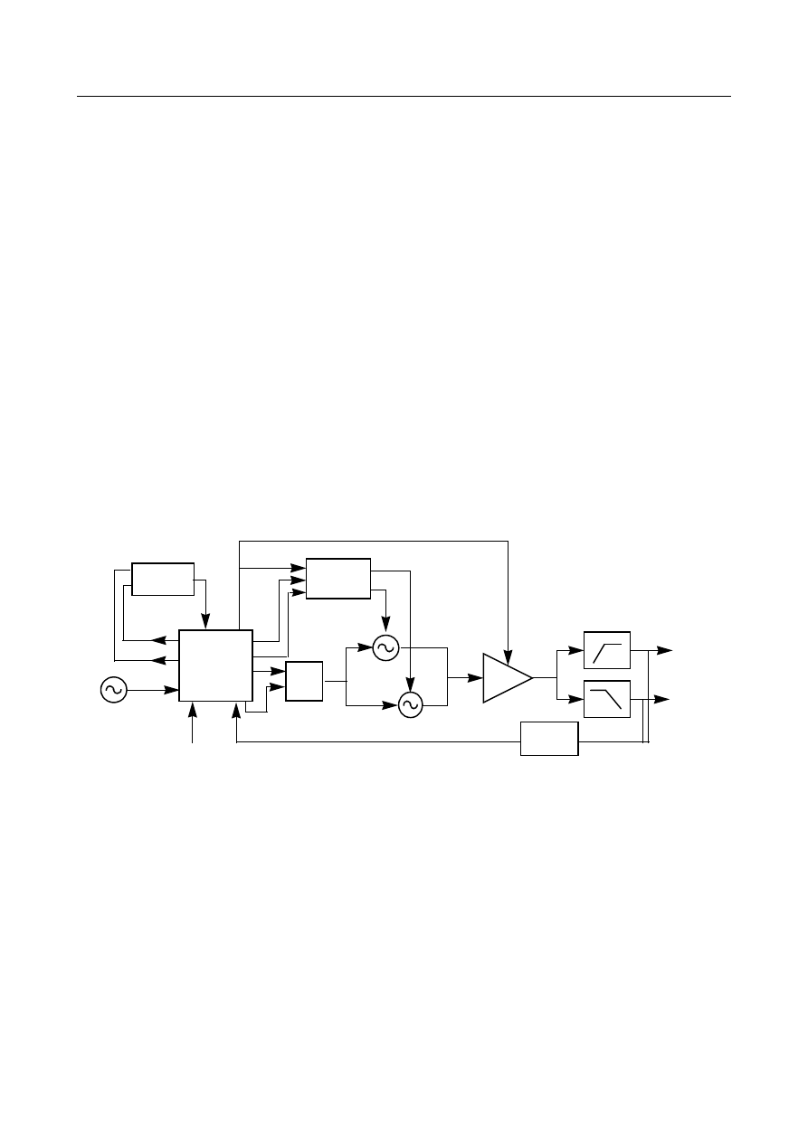
4.0
Frequency Generation Circuit
(Refer to Figure 2-3, the Synthesizer and Voltage controlled Oscillator schematic diagrams)
The frequency generation circuit is composed of Low Voltage Fractional-N synthesizer U205 and
discrete RX VCO, TX VCO and buffers as well other supporting circuitry. The synthesizer block
diagram illustrates the interconnect and support circuitry used in the region. Refer to the schematic
for the reference designators.
The synthesizer is powered by regulated 5V and 3.3V. The 5 volt signal to the synthesizer as well as
the rest of the radio is provided by U204. The 3.3 v signal is provided from U200 in the controller.
The 5V signal goes to pins 13 and 30 while the 3.3V signal goes to pins 5, 20, 34 and 36 of U201.
The synthesizer in turn generates a superfiltered 4.3V which powers the VCOs and buffers.
In addition to the VCO, the synthesizer also interfaces with the logic and ASFIC circuitry.
Programming for the synthesizer is accomplished through the data, clock and chip select lines (pins
7, 8 and 9) from the microprocessor, U409. A 3.3V dc signal from pin 4 indicates to the
microprocessor that the synthesizer is locked.
Transmit modulation from the ASFIC is supplied to pin 10 of U205. Internally the audio is digitized by
the Fractional-N and applied to the loop divider to provide the low-port modulation. The audio runs
through an internal attenuator for modulation balancing purposes before going out at pin 41 to the
VCO.
Figure 2-3 Lowband Frequency Generation Unit Block Diagram
Voltage
Multiplier
Synthesizer
U205
Loop
Filter
To
Mixer
To PA
Driver
VCP
Aux2
Aux3
MOD Out
Modulating
Signal
Vmult1
17.0 MHz
Ref. Osc.
Switching
Network
VSF
Prescalar input
TX VCO
RX VCO
Buffer
Vmult2
Amplifier
2-6
THEORY OF OPERATION
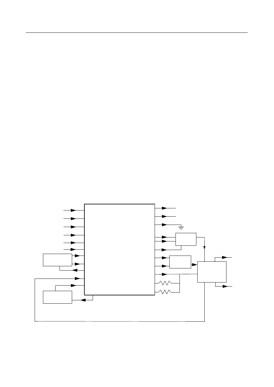
4.1
Synthesizer
(Refer to Figure 2-4 and the Synthesizer schematic diagram)
The Fractional-N synthesizer, shown in Figure 2-4, uses a 17.0 MHz crystal (Y201) to provide a
reference for the system. Along with being used in the LVFracN, the 17.0 MHz signal is provided at
pin 19 of U205 for use by the ASFIC and LVZIF.
The LVFractN IC (U205) further divides this by 8 internally to give 2.125 MHz to be used as the
reference frequency in the frequency synthesis. While UHF and VHF can use other references,
(divide by 7 or divide by 7/8), only the divide by 8 function is valid for lowband.
The internal oscillator device in the LVFracN together with C236, C237, C242, R219, CR211 and
Y201 comprise the reference oscillator. This oscillator is temperature compensated is capable of 2.5
ppm stability over temperatures of -30 to 85
°C. There is temperature compensation information that
is unique to each crystal contained on Y201 that is programmed into the radio when built.
The loop filter consists of components C256, C257, C259, R224, R225 and R228. This circuit
provides the necessary dc steering voltage for the VCO and determines the amount of noise and
spur passing through.
To achieve fast locking for the synthesizer, an internal adapt charge pump provides higher current at
pin 45 of U205 to put the synthesizer within lock range. The required frequency is then locked by
normal mode charge pump at pin 43.
Both the normal and adapt charge pumps get their supply from the inductive voltage multiplier made
up of C247, C249, C283-C286, D210, D211, R285 and R286.
This circuit provides 13.3V at U205, pin 47.
Figure 2-4 Lowband Synthesizer Block Diagram.
DATA
CLK
CEX
MODIN
V
CC
, DC5V
XTAL1
XTAL2
WARP
PREIN
VCP
REFERENCE
OSCILLATOR
VOLTAGE
MULTIPLIER
VOLTAGE
CONTROLLED
OSCILLATORS
2-POLE
LOOP
FILTER
DATA (U409 PIN 100
)
CLOCK (U409 PIN 1)
CSX (U409 PIN 2
)
MOD IN (U404 PIN 40)
+5V (U204 PIN 4)
7
8
9
10
13, 30
23
24
25
32
47
INDMULT
BIAS1
SFOUT
AUX3
AUX2
IADAPT
IOUT
GND
FREFOUT
LOCK
4
19
6, 17, 22, 29, 31, 33, 44
43
45
1
2
28
16
40
FILTERED 4.3V
STEERING
LINE
LOCK (U409 PIN 56)
PRESCALER IN
LO RF INJECTION
TX RF INJECTION
(FIRST STAGE OF PA)
FREF (U303 PIN 21 & U404 PIN 34)
39
BIAS2
41
SWITCHING
NETWORK
5, 20, 34, 36
(U400 PIN 1)
V
DD
, 3.3V
MODOUT
U205
LOW VOLTAGE
FRACTIONAL-N
SYNTHESIZER

Frequency Generation Circuit
2-7
4.2
Voltage Controlled Oscillator (VCO)
(Refer to the Voltage Controlled Oscillator schematic diagram)
4.2.1
Receive VCO
The receive VCO is a Colpitts type design and using two active devices in parallel, Q202 and Q204.
The oscillator is powered off of the 4.3 volt super filter supply when the AUX3 line goes low. The
oscillator operates from 139 to 152 MHz for range 1 and 145 to 160 MHz for range 2. The frequency
is tuned by varactor diodes CR201 and CR202.
4.2.2
Transmit VCO
The transmit VCO is a Hartley type design with active devices Q203. The oscillator is powered off of
the 4.3 volt super filter supply when the AUX2 line goes low. The oscillator operates from 29.7 to 42
MHz for Range 1 and 35 to 50 MHz for Range 2. The frequency is tuned by varactor diodes in U203.
Note that the values of the inductive tap, L208 and L209, and the capacitor C215 which couples the
varactor to the oscillator tank vary between the ranges.
4.2.3
Buffer
Both the receive and transmit VCO are fed to a buffer amplifier Q201. This is a BJT amplifier that
boosts the signal levels to +4 dBm and provides reverse isolation to the oscillators. The amplifier is
powered off the 4.3 volt super filter supply and the feed network is combined with the transmit filter.
4.2.4
Diplexer and Output Filters
The output of the buffer drives a pair of parallel filters. One filter is a lowpass filter in the TX path that
passes 29.7 - 50 MHz signals for the transmitter into the power amplifier while rejecting the receive
LO injection signals at 139 - 160 MHz. This filter is comprised of L204, L211, L212, C230 and C231.
The other filter is a highpass filter which passes 139 - 160 MHz signals for the receive LO into the
mixer while rejecting the transmit injection signals at 29.7 -50 MHz. This filter is comprised of
C228,C229,C235 and L215.
4.2.5
Prescaler Feedback
The prescaler input signal for receive and transmit is tapped off the outputs of each filter by resistors
R234 and R238. This signal is routed to the buffer amplifier consisting of components C287, Q288,
R287, R288 and R289. The output of this buffer feeds U205 pin 32. After frequency comparison in
the synthesizer, current is transferred in the loop filter and a control voltage is generated at the
output of the loop filter to adjust the frequency of the VCO. This voltage is a DC voltage between
3.5V and 9.5V when the PLL is locked on frequency.

2-8
THEORY OF OPERATION
Chapter 3
TROUBLESHOOTING CHARTS
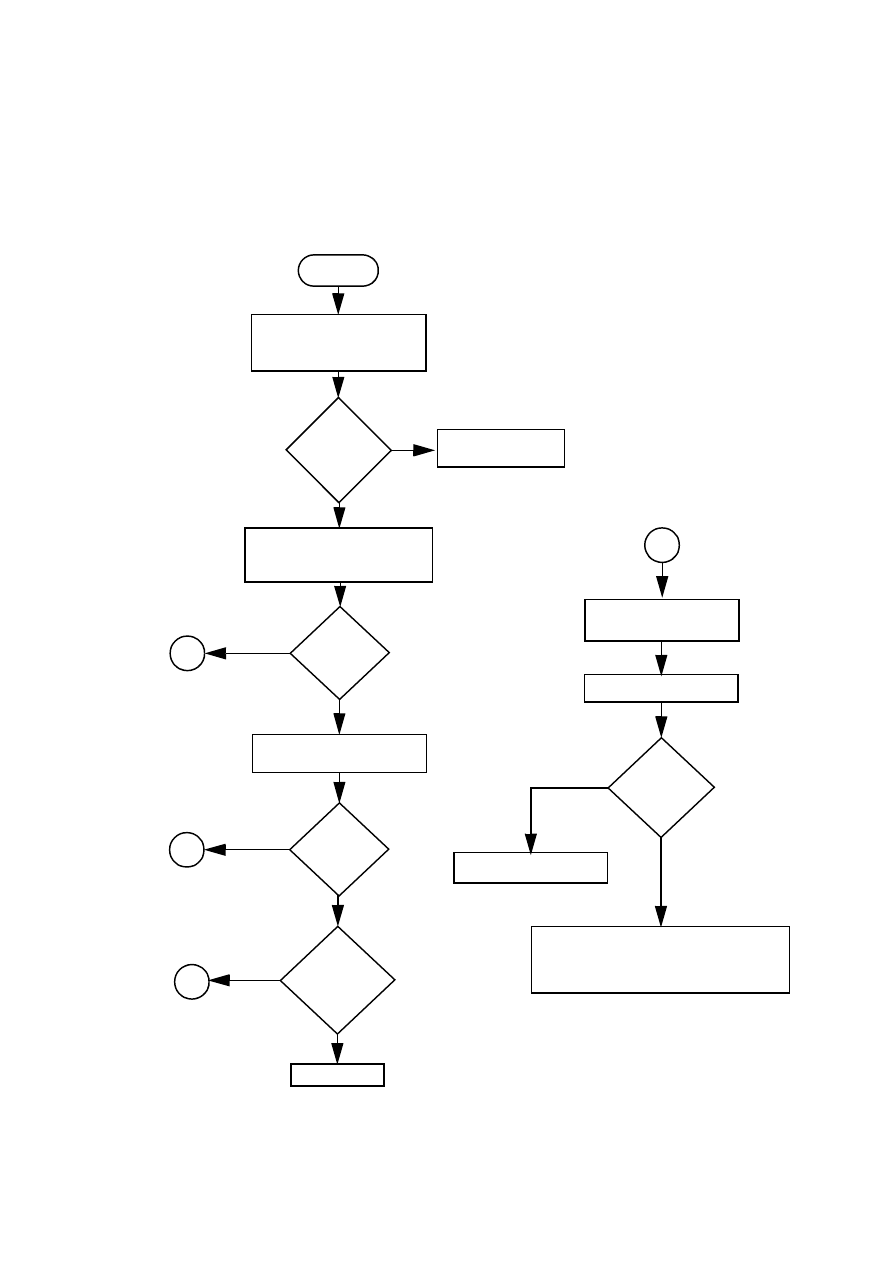
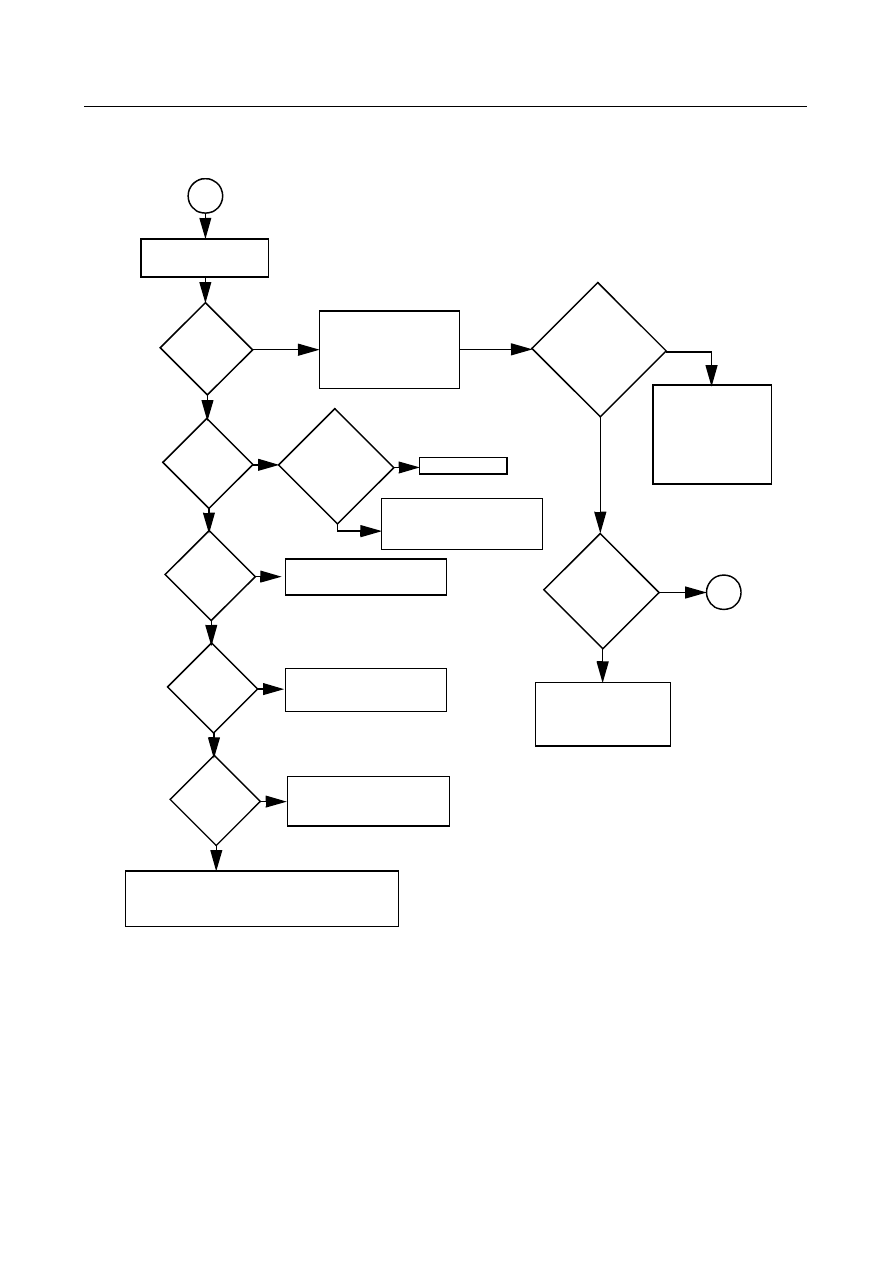
1.0
Receiver (Sheet 1 of 2)
VCO
locked?
Bad SINAD
Bad 20dB Quieting
No Recovered Audio
START
Audio at
pin 27 of
U303?
Check Controller
Yes
No
Spray of inject 1st IF into
XTAL Filter
IF Freq: 109.65 MHz
Audio
heard?
B
Yes
No
Check 2nd LO Control
Voltage at C308
B
Yes
17.0 MHz
check at pin
22 U303?
Activity
on U303
sel pin?
Check FGU
No
No
A
A
Yes
Check Q301 bias
circuitry for faults.
Rotate Freq. Knob
Check controller.
Before replacing U303, check 2nd
VCO Q301. Check VCO O/P level,
C315, C316.
Yes
No
3-2
TROUBLESHOOTING CHARTS
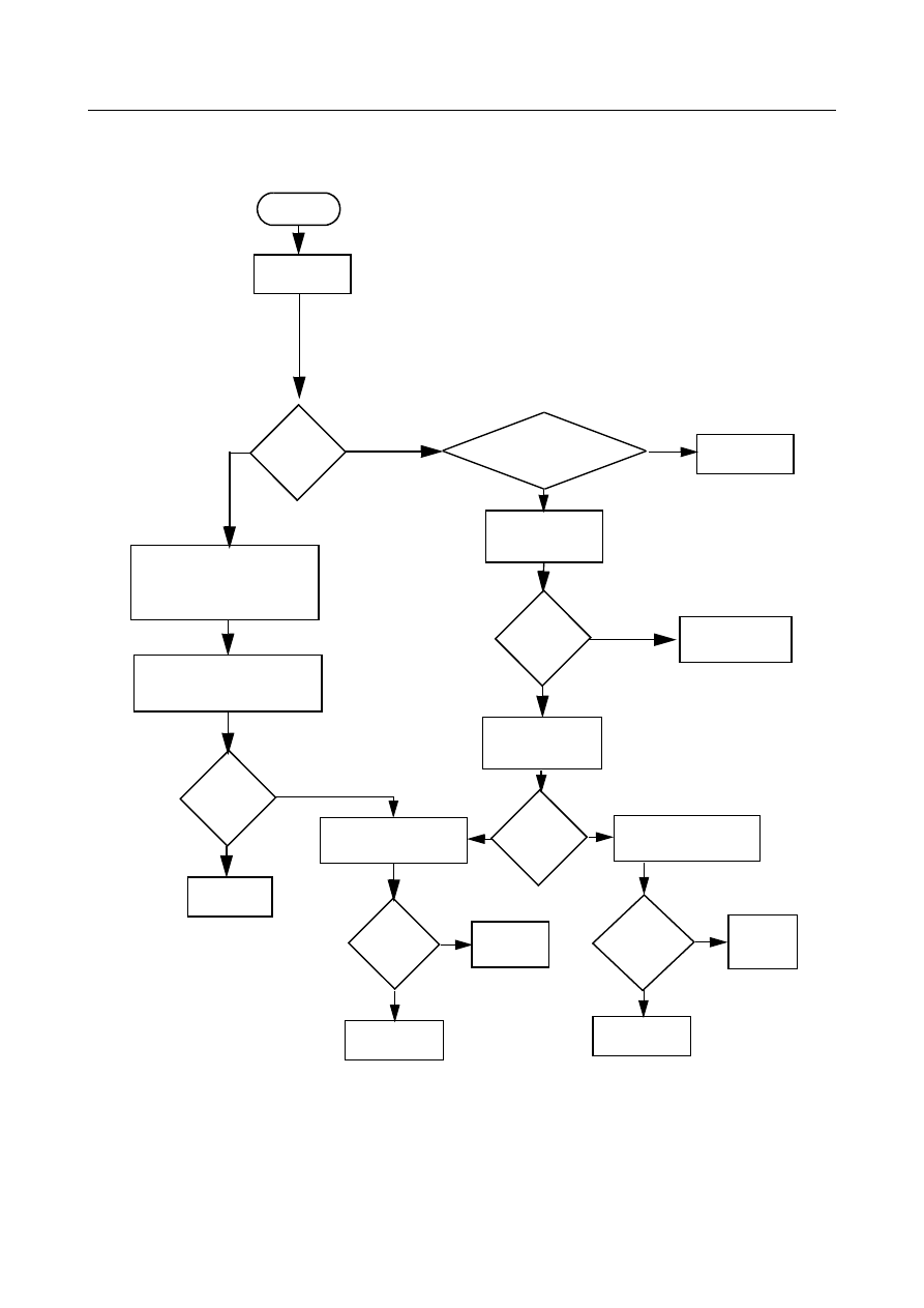
2.0
Receiver (Sheet 2 of 2)
RF
Signal at
collector
Q509?
IF
signal at
L301?
No
RF
Signal
at T501?
No
RF
Signal at
C504?
No
RF
signal at
C147?
No or
Check transmit harmonic filter, antenna
switch and J101
Check filter between
C147 & C504
Inject RF into J101
No
Yes
Check RF amp (Q509)
Stage.
Check filter between
Q509 and T301.
Yes
Check T501, T502,
D501, R507, R508,
R509, C516 and L508
Yes
1st LO O/P
310 OK?
Locked?
Yes
Check FGU
Yes
Trace IF signal
from L301 to U301.
Check for bad
XTAL filter.
No
Yes
U301 drain
OK?
IF signal
present?
Before replac-
ing U303, check
U303 voltages;
trace IF signal
path.
Yes
Biaising on
U301 OK?
Troubleshoot
biasing, AGC
circuits and U301
No
No
Yes
A
B
weak RF
Transmitter
3-3
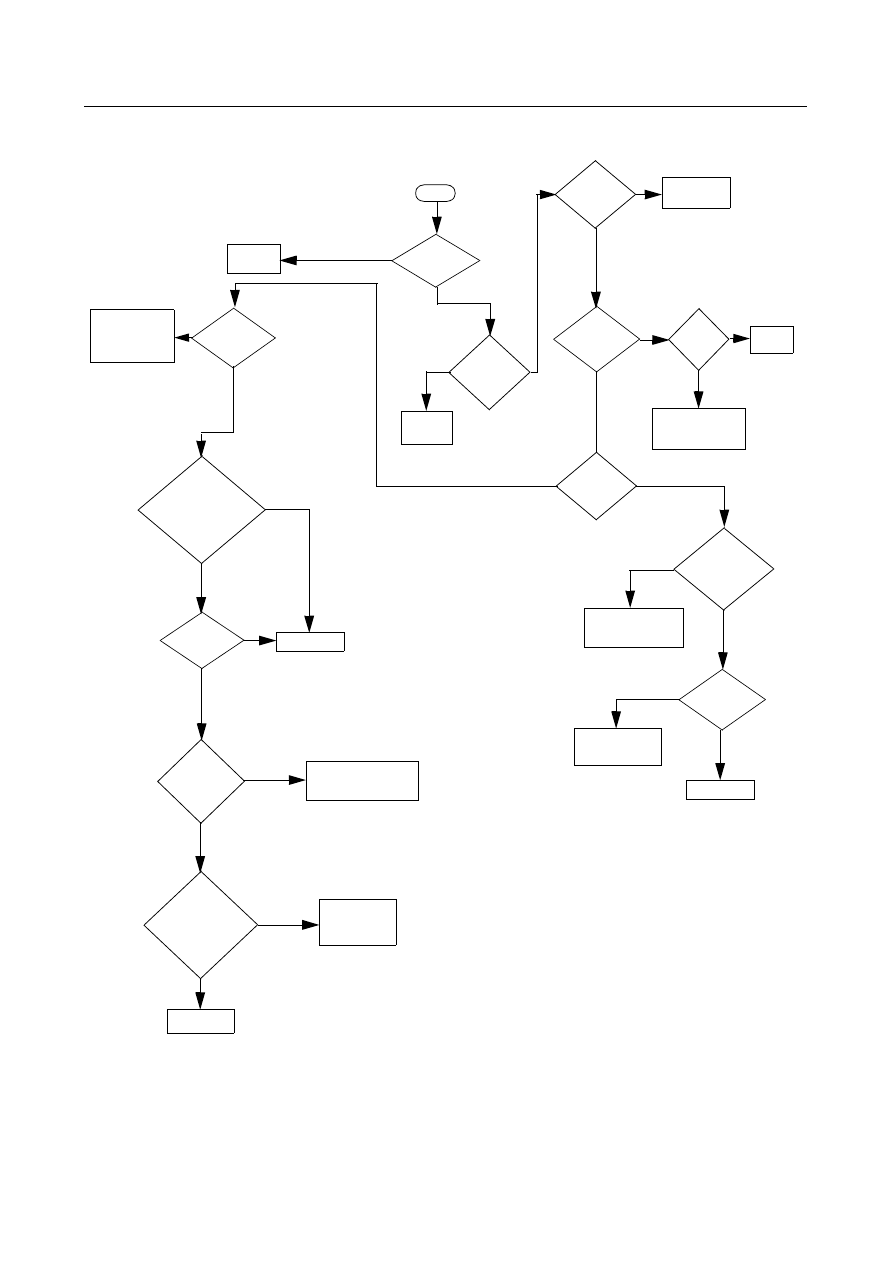
3.0
Transmitter
START
No Power
Is Current
~ 2 A?
Is control voltage
at U101 Pin 1 > 5
Check PCIC
1. Check Pin Diodes
2. Check Harmonic Filter
3. Check PA Bias
Inspect/Repair Tx.
Output Network
Is Power
OK?
Done
Check input to
U101, Pin 16
Is voltage
> 1 Vpp?
Troubleshoot
VCO
Check level
U101, Pin 6
Is level
>5 Vpp?
Is Power
OK?
Replace
Q101
Yes
No
No
Yes
No
Yes
No
Yes
Yes
No
Yes
No
Check components
around U101
Is Power
OK?
Done
Replace
U101
No
Check components
around Q100
Yes
Done
3-4
TROUBLESHOOTING CHARTS
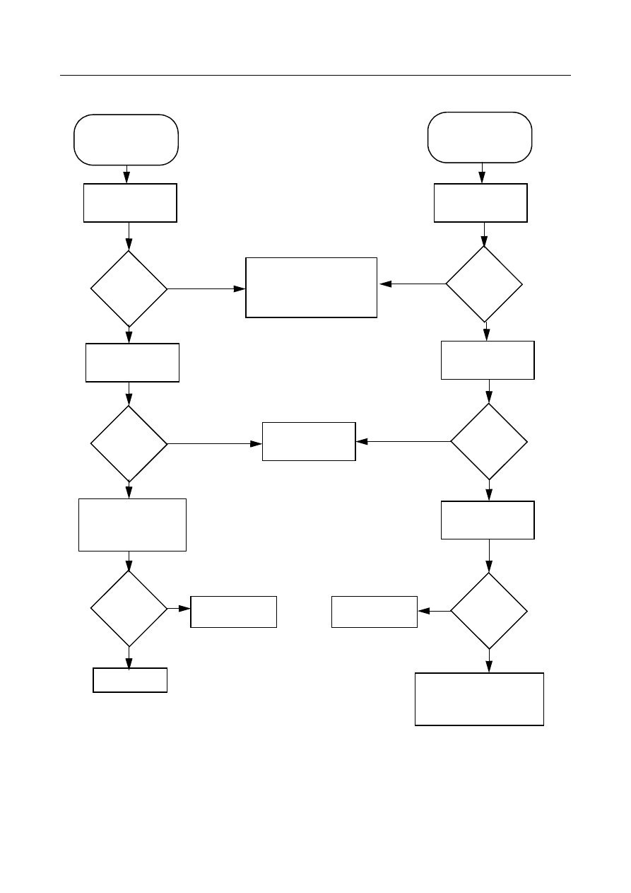
4.0
Synthesizer
Visual
check of the
Board OK?
+5V at
U205 Pin’s
13 & 30?
Is information
from
uP U409
correct?
Is U205
pin 18 at
4.54 V DC
?
Is U205
Pin 47 at
>12 V DC
In receive, is
Pin 1 < .7 V and Pin 2 >
3 Vplus in transmit is
Pin 1 > 3 V and Pin 2 <
.7 V?
Start
Correct
Problem
Check 5V
Regulator
Is 17.0 MHz
Signal at
U205 Pin 19?
Check Y201,CR211,
C236,C237,C242,
R219
Signal
at Pin 14 and
15 of U205?
Replace U205
Replace or
resolder
necessary
components
Is RF level at
U205 Pin 32
>-30 dBm?
Are loop filter
parts R224, R225,
R227, R228, R229,
C256, C257, C259
and C260
OK?
Replace U201
If R234, R238 and C297
are OK, then see VCO
troubleshooting chart
Do Pins 7,8 & 9
of U205 toggle
when channel is
changed?
Check programming
lines between U409
and U205 Pins 7,8 & 9
Replace U205
Check uP U409
Troubleshooting
Chart
NO
YES
NO
YES
NO
NO
YES
NO
YES
YES
NO
YES
YES
YES
NO
NO
NO
NO
YES
NO
YES
YES
Check C247, C249,
C283-C286,
D210, D211,
R285 and R286
3.3V at U205
pins 5, 20, 34
& 36
Check U400
and L225
Is
17.0MHz
signal at
U201 pin
23?
Replace
U205
YES
NO
NO
YES
Voltage Controlled Oscillator
3-5
5.0
Voltage Controlled Oscillator
Level >
+2 dBm
Check signal at
collector of Q201
No
Yes
Check L204, L211, L212,
L215, C221, C228, C229,
C230,C231, C235,C297,
R204, R234, R238
Check signal at
collector of Q201
No RX LO or No
signal at U205 Pin
32 in RX
No TX LO or No
signal at U205 Pin
32 in TX
Level >
+10 dBm?
Check signal at
drain of Q203
Level >
-3 dBm?
Check signal at
drain of Q202
and Q204
Level >
+7 dBm?
No
Yes
Replace Q201
Yes
Yes
Done
Check DC volt-
age across R203
Problem
fixed?
Replace Q203
Check C215, C216,
L207, L208, L209,
U203
Level >
500 mV ?
Check C200, C202, C203,
C222, C223, L201, L203,
TR201, CR202
Replace Q202
and Q204
Yes
Yes
No
No
No
No

3-6
TROUBLESHOOTING CHARTS

Chapter 4
LOWBAND PCB/SCHEMATICS/PARTS LIST
1.0
Allocation of Schematics and Circuit Boards
1.1
Controller Circuits
The Lowband circuits are contained on the printed circuit board (PCB) which also contains the
Controller circuits. This chapter shows the schematics for the Lowband circuits only, refer to the
Controller section for details of the related Controller circuits. The PCB component layouts and the
Parts Lists in this chapter show both the Controller and Lowband circuit components. The Lowband
schematics and the related PCB and parts list are shown in the Table below.
Table 4-1 Lowband Diagrams and Parts
PCB : 8485658Z03
Main Board Top Side
Main Board Bottom Side
Page 4-3
Page 4-4
SCHEMATICS
Receiver Overall Schematic
Receiver Front End
Receiver Back End
Synthesizer
Voltage Controlled Oscillator
Overall Synthesizer Schematic
Transmitter
Page 4-5
Page 4-6
Page 4-7
Page 4-8
Page 4-9
Page 4-10
Page 4-11
Parts List
Page 4-12

4-2
Lowband PCB/SCHEMATICS/PARTS LIST
Wyszukiwarka
Podobne podstrony:
B32E Sect8 LoBand A3
B32E Sect7 300MHz A4
podciag a4
2013.09.17 FORMATKA RYSUNKOWA A4
A4, Akademia Morska -materiały mechaniczne, szkoła, Mega Szkoła, PODSTAWY KON, Program do obliczeń P
tab imip a4, AiR WIP, IV semestr, PRZTS Przetwórstwo tworzyw sztucznych, projekt
K 4 Pręt p1 A4
a4 (4)
AUDI A4 8E 2005pl
karny kutas za parkowanie A4 druk
audi A4 6 stala praca wentylatora chlodnicy
Cyfry pisane w formacie A4
2007 12 27 19 35 warminsko mazurskie A4
a4
Instrukcja CCD 2001 w 1000, A4, W2 04
więcej podobnych podstron