
1
Triplets Baseband
Overview
Edwin Gonzalez

2
Motorola Confidential Proprietary
Regulators
Vbuck, 1.875V +/- 4%
Sources Neptune Core
Vboost 5.6V +/- 5%
Source for V10 & keypad backlights
V1 = I/O REG, 2.875V +/- 3%, Neptune I/O Reg 2.875 +2/-4%
Sources Neptune I/O, ATI Graphics Accel I/O Ring, Camera, SPI interfaces
V3 = VA1.2, Starts at 1.575V then SW selected to 1.275 +/-3%
Sources ATI Graphics Accel core
V4/V5 = tied to V1,
programmed to OFF, but source internal PCAP
circuitry
V6 = NC
V7 = RF_REG, 2.875V +/- 3%
Sources Algae and Support circuitry.
V8 = BTRF, 1.875V +/- 3%
Sources Blue Tooth circuitry
V9 = REF_REG, 1.575 V +/- 3%
RTC and Neptune reference
V10 = RF_5V_REG, 5V +/- 3%
3
Motorola Confidential Proprietary
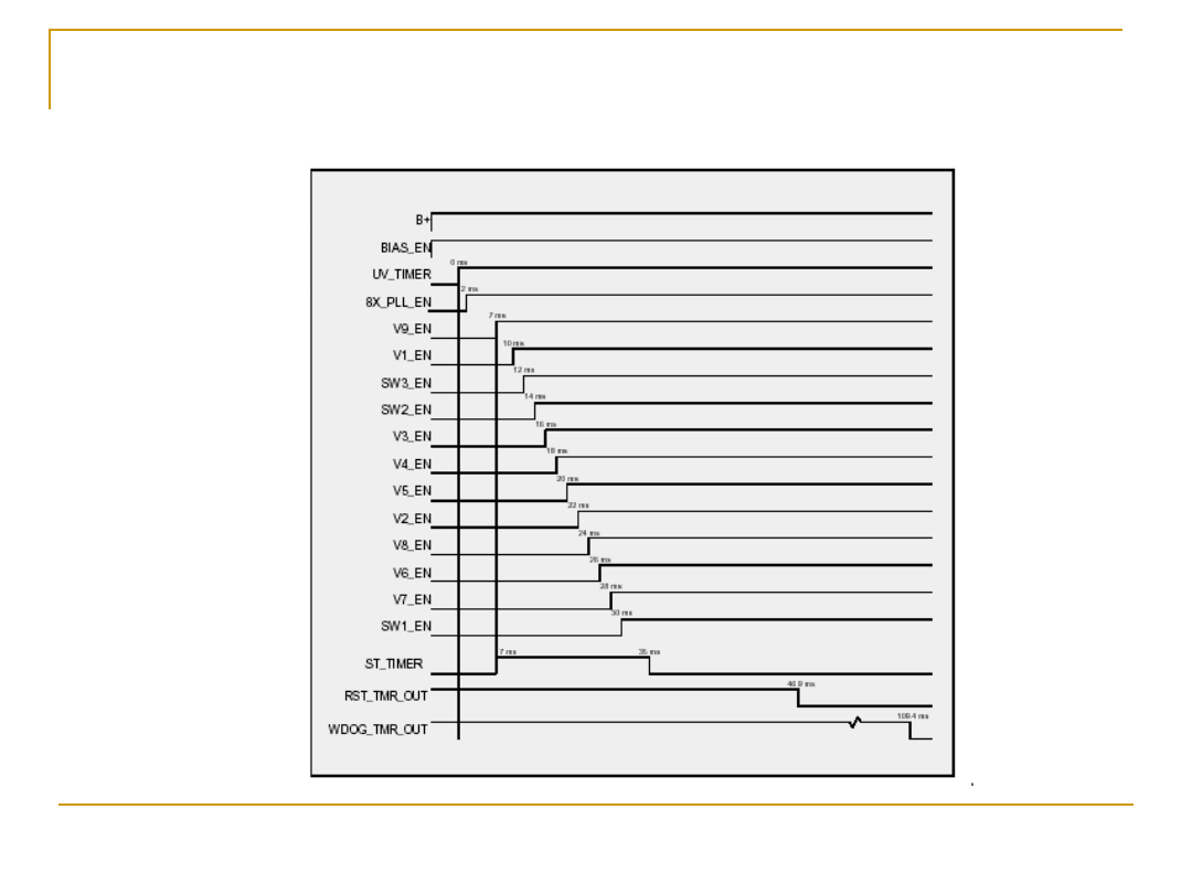
PCAP Regulators Sequencing

4
Motorola Confidential Proprietary
Charger
Works exactly the same as the P2k products
All the FETS are PFETs
Charger FET runs linearly with all chargers, PCAP controls
Gate voltage based on Voltage Sense across Sense Resister
Midrate FET– Allows for connection of the charger to the
phone
Main FET– controls whether battery is connected to the
phone,
OVIC– Threshold is 6.9+/- 0.2V
Fast Rate Charger, OVIC is ON
Charger is in Linear mode passing ~500mA
Midrate FET is ON
Main FET is OFF
When phone is active it pulls all the current from the
charger, and left over will continue to charge the battery.

5
Motorola Confidential Proprietary
Charger –Cont’d
Midrate Charger , while phone is in standby or Charge
only mode
OVIC is ON
Charger is in linear mode, the amount of current passing
from charger to battery is dependent upon battery voltage
Main FET is OFF
Midrate Charger, While in a call or using camera/pda/or
other high current tasks
OVIC is ON
Midrate is OFF
Charger is in linear mode
Main FET is ON
This particular mode of the charger is not fully implemented
in the SW and the HW engineers are currently working
through the details of what the phone should do under
different load conditions. Follow up material will need to be
completed once these details have been worked out.
6
Motorola Confidential Proprietary
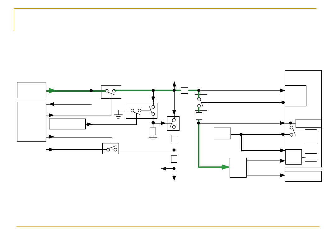
Charger
RAW_EXT_B+
EXT_B+
B+
ISENSE
CHRGC
BATT+
MAIN_FET
BATT+
Q953
Q951
R951
VR950
R950
Q950
VR961
Q952
Q954
OV_GATE
OV_SENSE
PCAP
U900
MIDRATE_1
PCAP
U900
CE
Conn
Charger
BATT_FDBK
AD6
BATT_THERM
CE
Conn
SPI
MUX
BattSense
OWB
NEPTUNE
Batt
Conn
SPI
L950
PA_B+
NEPTUNE
7
Motorola Confidential Proprietary
off of a P2K compatible
battery thermister
Put L950 choke close to PCAP
Note: package and resistor
Overvoltage Protection
Dual Path
will be moved
Therm_Bias
Battery Charge Circuit
R956 and R957 values are based
into A07
3
1
4
Q
95
1
2
5
6
2113743L35
C951
value=5600pF
N
C
R951
value=10K
C911
value=.01uF
N
C
0662057N34
R957
value=300K
N
C
N
C
value=.24
R950
0687874L01
Q952
value=10K
R916
C900
value=0.1uF
R955
2113743M24
value=10K
0662057M98
value=0
0662057M01
R900
N
C
value=0.1uF
C940
C950
value=0.1uF
2113743M24
VOLTAGE
VR950
NC
NC
N
C
NC
NC
C
R
92
0
R906
value=39K
N
C
0662057M92
R958
value=5.6K
R952
0662057V35
value=200K
N
C
value=10uF
NC
C952
2113928C13
R
90
5
va
lu
e=
10
K
4889091N01
VOLTAGE
VR951
CR900
0662057N06
value=20K
R956
Q953
4809807C41
Q950
C953
2113928A01
value=1.0uF
N
C
N
C
R
91
7
va
lu
e=
10
K
W
D
I
TSX2
TSY1
TSY2
U
S
R
_O
F
F
U
V
_S
E
L
S
T
A
N
D
B
Y
T
H
E
R
M
_B
IA
S
TSX1
PSRC1
PSRC2
R
E
S
E
T
B
R
E
S
E
T
M
C
U
_B
PGND1
P
O
W
E
R
_F
A
IL
O
N
O
N
2
O
V
_G
A
T
E
O
V
_S
E
N
S
E
M
A
IN
_F
E
T
M
F
E
T
_L
O
W
M
O
B
P
O
R
T
B
M
O
D
M
U
X
_C
T
R
L
IN
T
_P
R
I
IN
T
_S
E
C
IS
E
N
S
E
LE
D
G
LE
D
R
LX1A
LX1B
FB1
B
O
B
_B
U
C
K
N
B
O
B
_B
U
C
K
P
B
O
B
_V
D
D
1
B
O
B
_V
D
D
2
B
O
B
_V
O
U
T
+
B
O
B
_V
O
U
T
-A
B
O
B
_V
O
U
T
-B
B
O
B
_V
R
E
F
+
B
O
B
_V
R
E
F
-
B
O
B
_V
S
S
1
B
O
B
_V
S
S
2
B
O
B
_V
S
W
1
B
O
B
_V
S
W
2
C
H
R
G
C
B
+
B
A
T
T
+
B
A
T
T
_D
E
T
B
B
A
T
T
_D
E
T
_I
N
B
A
T
T
_F
D
B
K
B
L2
_S
IN
K
B
L_
F
B
B
L_
S
IN
K
B
O
B
_B
O
O
S
T
N
B
O
B
_B
O
O
S
T
P
AD4
AD5
AD6
AD7
AD8
AD9
AD_TRIG
Q954
4809807C41
N
C
BATT+
B
A
TT
+
M
ID
R
A
T
E
_1
M
ID
R
A
T
E
_1
MIDRATE_2
W
D
O
G
B+
B
+
RAW_EXT_B+
EXT_B+
E
X
T
_B
+
B
A
TT
_F
D
B
K
IO
_R
E
G
PA_B+
IO
_R
E
G
N
E
P
_I
O
_R
E
G
B
L_
F
B
B
A
T
T
+
O
N
2
B
L_
S
IN
K
P
W
R
_S
W
NEP_IO_REG
B
A
T
T
_D
E
T
B
THERM
R
E
S
E
TB
RESETB
B+
AD_TRIG
S
TA
N
D
B
Y
B+
B
+
B
L2
_S
IN
K
P
C
A
P
_I
N
T
Charger
8
Motorola Confidential Proprietary
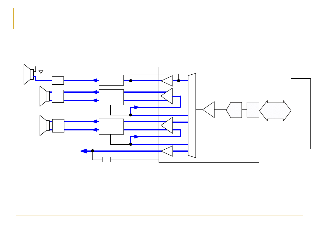
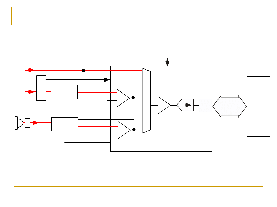
RX Audio
P C A P
S P K R O U T 2
A L R T _ IN
E X T O U T
A u d i o F il te r
C ir c u it
A L R T -
A L R T +
L o u d s p e a k e r
O N 2
R 1 0 5 5
N E P T U N E
S S I
BB_SAP_RX
BB_SAP_CLK
BB_SAP_FS
1 3 - b i t
P h o n e
D A C
J 1 2 6 0
ARIGHT_IN
ARIGHT_OUT
PGA
A u d i o F il te r
C ir c u it
HJ ACK_SPKR
H e a d s e t
S p e a k e r
S S I1
S P K R O U T 1
S P K R _ I N
A u d i o F il te r
C ir c u it
S P K R -
S P K R +
H a n d s e t
S p e a k e r
A 1
A U D I O _ O U T
A 2
A 4
ALRT-
ALRT+
J 1 3 0 0
HAND_SPKR-
HAND_SPKR+
J 1 2 4 0
A
U
D
M
U
X
9
Motorola Confidential Proprietary
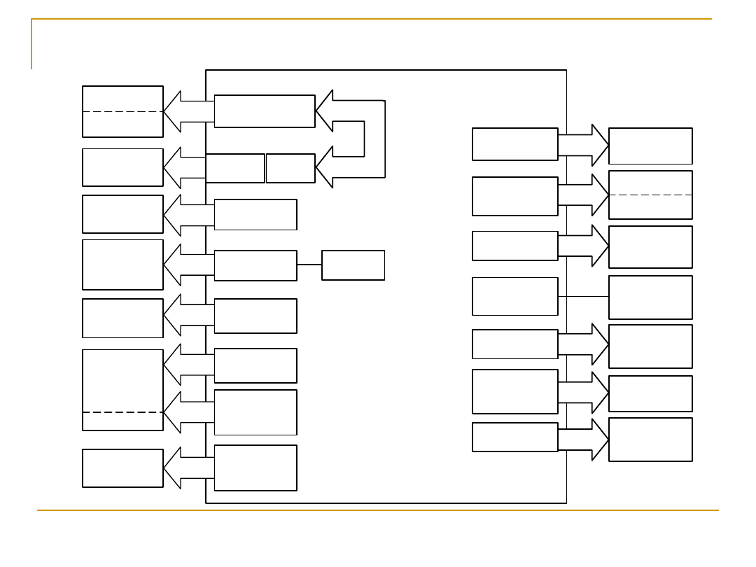
TX Audio
M IC G A IN
P C A P
L O G IC _ S E N S E
M IC _ B IA S 1
A U X _ O U T
A U X _ M I C -
A u d io F i lt e r
C i r c u i t
M IC
A D C
N E P T U N E
P G A
A U D I O _ I N
M IC _ B IA S 2
M IC _ O U T
A u d io F i lt e r
C i r c u i t
A
U
D
M
U
X
H S _ M IC
S S I
MM_SAP_TX
MM_SAP_FS
MM_SAP_CLK
J1
24
0
J 1 2 0 0
A 5
A 3
H S _ M A K E _ D E T E C T
E X T _ M I C
V A G
V A G
M I C _ IN -
10
Motorola Confidential Proprietary
PCAP
B a s e b a n d
C i r c u i ts
R F I n te r f a c e
L o g i c I n te r f a c e
R e g u la to r
In te r f a c e
B a c k l i g h t
S ta tu s
L E D s
L i n e a r
R e g u l a to r s
C o n tr o l
L o g ic
S w i tc h in g
R e g u la to r
L E D
D r i v e
B a c k l i g h t
C o n tr o l
N E P T U N E
P o w e r C u t
P o w e r F a il
H a n d l i n g
X T A L
C o in C e l l
I n t e r f a c e
S p e a k e r C k t s
M i c C k t s
C h a r g e r
L o g i c
In te r f a c e
N E P T U N E
S P I
I n te r f a c e
C h a r g e r
C o n t r o l
M u l t i p le x e r
A u d i o
A m p l if i e r s
U S B
R S 2 3 2
B u s
C O D E C
A /D
S S I
I n te r f a c e
O v e r v o lta g e
P r o te c ti o n
C E B u s
N E P T U N E
U S B
O n - t h e - G o
C E B u s
NEPTUNE
Bluetooth
U900

11
Motorola Confidential Proprietary
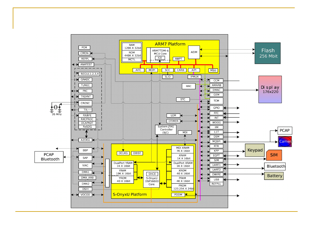
Neptune LTE (U800)
RF connection is same as with LCA architecture
PCAP interface is very similar to P2K, uses a SPI to read
and write registers, & variety of port lines to pass data.
Display and Camera are interfaced through the ATI
Graphic Accelerator. Data is passed to the Graphic Accel
through the DMAC of Neptune. Data is passed back to
Neptune through the SPI. All direct control of the camera
and display is handled by ATI part.
Funlights/LCD Backlights driver is controlled via SPI,
same SPI for PCAP & ATI part.
Bluetooth connections is through a UART.
Keypad, is same implementation as on P2K products
CE Bus should behave same as it does for P2K
12
Motorola Confidential Proprietary
Neptune LTE (U800)

13
Motorola Confidential Proprietary
26 MHz Clock, Y805
This clock is required for Neptune to
come up fully and run at full speed.
Without the presence of this clock the
phone will start to power up and
immediately shut down. No
communication with Neptune will be
available
This clock is also used by TXVR and
must be very clean.

14
Motorola Confidential Proprietary
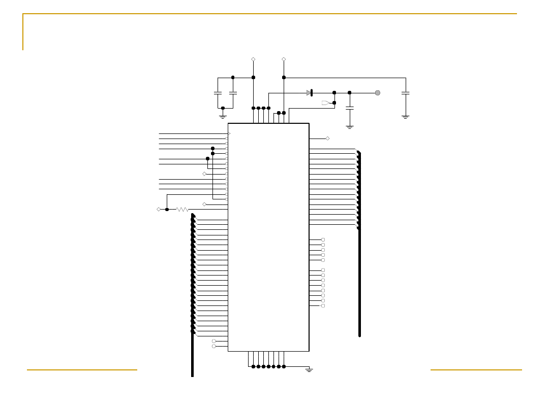
Flash/SRAM Memory, U700
Triple stack part
Two Tyax 128Mbyte Flash
One PseudoSRAM 32Mbyte
IMEI is stored in the FLASH
Replacing Neptune or Memory Device
Neptune and Memory are under a shield and possible to
replace, but difficult. If Field service chose to replace
FLASH, IMEI would need to be reprogrammed.
Neptune is a 280 pin bga, difficult to replace, but possible.
There are new Security enhancements that are not fully
implemented yet.
15
Motorola Confidential Proprietary
Note: Present pass will not
support power cuts.
NC
NC
2113743M24
VALUE=0.1uF
C701
2
1
14
NC
5
2
3
4
5
6
7
8
0
9
10
11
12
13
14
15
1
19
NC
NC
NC
24
18
16
NC
2
NC
21
NC
NC
10
22
2113743M24
C700
VALUE=0.1uF
2
1
1
13
TP _VPP
11
NC
R
70
7
V
A
LU
E
=0
9
NC
17
3
15
VALUE=0.1uF
C704
6
NC
8
NC
1
NC
7
VALUE=0.1uF
C703
D700
20
23
4
12
L
2
L
5
V
S
S
5
V
S
S
6
L
6
L
7
V
S
S
7
V
S
S
8
L
8
WAIT
G7
WE_
F5
WP_
E4
K
6
V
C
C
Q
_1
J8
V
C
C
Q
_2
K
7
L
3
V
C
C
Q
_3
D
4
V
P
P
B
4
V
S
S
1
V
S
S
2
C
4
L
1
V
S
S
3
V
S
S
4
R_UB_
R_WE_
D5
S_CS1_
J 1
C5
S_CS2
K4
S_VCC
V
C
C
1
_1
B
5
L
4
V
C
C
1
_2
V
C
C
2
_1
B
6
V
C
C
2
_2
P_CS_
P_MODE
K8
K5
P_VCC
K2
RFU1
RFU2
K3
RST_
F4
R_LB_
C2
H1
R_OE_
F3
DU3
DU4
A8
M1
DU5
DU6
M2
M7
DU7
DU8
M8
OE_1
J 2
H8
OE_2
D6
D4
G5
D5
J 6
D6
H7
D7
G2
D8
J 3
D9
A1
DU1
DU2
A2
A7
D10
J 4
D11
H5
D12
G6
D13
H6
D14
J 7
D15
G3
D2
H4
D3
J 5
A8
D7
A9
E5
ADV_
CE_1
K1
G8
CE_2
CLK
C6
H2
D0
H3
D1
G4
A23
D3
A24
E3
A25
D1
A3
B1
A4
C1
A5
F2
A6
E2
A7
F6
A16
D2
A17
A18
B2
A19
B3
E1
A2
A20
E6
A21
B7
C7
A22
C3
G1
F1
A1
E7
A10
B8
A11
C8
A12
D8
A13
F7
A14
E8
A15
F8
VPP_SIGNAL
RD38F3340LLYDQ0
U700
A0
V
B
U
C
K
V
B
U
C
K
A
D
D
R
E
S
S
(2
4
:1
)
VBUCK
VBUCK
RESET_OUT
D
A
T
A
(1
5
:0
)
ECBB
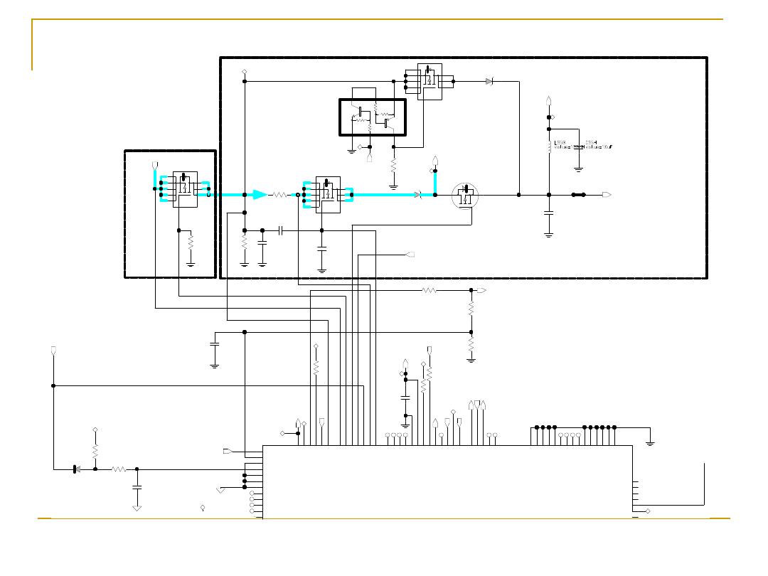
Flash/SRAM Memory, U700
16
Motorola Confidential Proprietary
Bluetooth System Block
Neptune
LTS/LTE
95L14
Bluetoo
th
Module
PCAP
BTRF_REG = 1.8VDC
UART
2
SAP
BLUE
WAKE
26MHz
XTAL
BLUE HOST WAKE
26MHz
XTAL
IO_REG = 2.775VDC
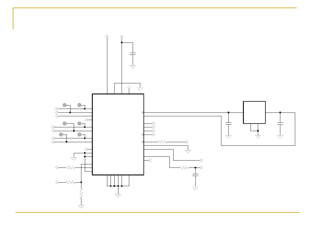
17
Motorola Confidential Proprietary
ground
R301DNP
ground
C360
VALUE=0
VALUE=4.7uF
C302
VALUE=18pF
R330
VALUE=390K
TPBLUE_CTSB
1
NC
VALUE=0.5pF
VALUE=10K
C320DNP
1
R303
TPBLUE_HW
ground
C301
VALUE=18pF
TPBLUE_RTSB
1
1
ground
ground
10
V
_I
_O
16
XTAL_IN
XTAL_OUT
15
TPBLUE_W
TM0
18
TM1_2
19
TM3
20
TX_PU_TDD_N
23
USB_DETACH
8
USB_DN
3
USB_DP
4
V
D
D
_U
S
B
2
7
EEPROM_CLK
G
N
D
1
1
G
N
D
2
14
G
N
D
3
17
G
N
D
4
24
G
N
D
5
26
LPO_INA
6
RESET_N
22
BLUE_RTS
31
33
BLUE_RX
BLUE_TX
5
BLUE_WAKE
11
34
B
T
L
_R
E
G
B
T
R
F
_R
E
G
21
12
CLK_32_768K
C
T
G
N
D
35
ANTENNA_MATCH
25
ASAP_CLK
27
ASAP_FS
28
ASAP_RX
30
32
ASAP_TX
BLUE_CLK_EN
13
BLUE_CTS
29
9
BLUE_HOST_WAKE
NC
U301
95L14
1
ground
ground
TPBLUE_RX
TPBLUE_TX
1
ground
NC
ground
R320
VALUE=0
R302
VALUE=10K
G
N
D
1
2
4
G
N
D
2
HOT1
1
HOT2
3
ground
OUT1-2B-2757
Y300
BLUE_RX
N
E
P
_I
O
_R
E
G
NEP_IO_REG
NEP_IO_REG
N
C
BB_SAP_CLK
BB_SAP_FS
BB_SAP_RX
BB_SAP_TX
BLUE_CLK_ENB
BT_ANTENNA
B
T
R
F
_R
E
G
BLUE_RESETB
BLUE_TX
BLUE_CTSB
BLUE_RTSB
BLUE_WAKEB
BLUE_HOST_WAKEB
CLK_32KHZ
Bluetooth

18
Motorola Confidential Proprietary
Flip LCD Modules
This display is a color Active Matrix Liquid Crystal Display
(AMLCD) module of glass construction with black pixels
on a white background.
The display consists of 176 (x RGB Stripe) x 220 pixels
with 64K colors.
There are a few different displays from different vendors
Samsung TF, Samsung TMR and Sharp TF
The Samsung TF and Sharp TF will be used on V300 &
V600 (Only on V300 the situational lighting tail will be
cutoff)
The Samsung TMR is a 98% transmissive display that w/o
the LCD backlight the display is completely black.
19
Motorola Confidential Proprietary
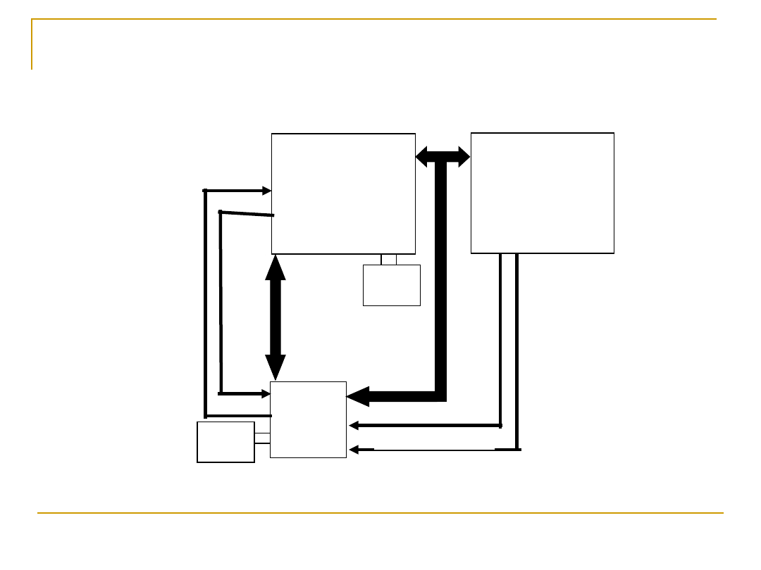
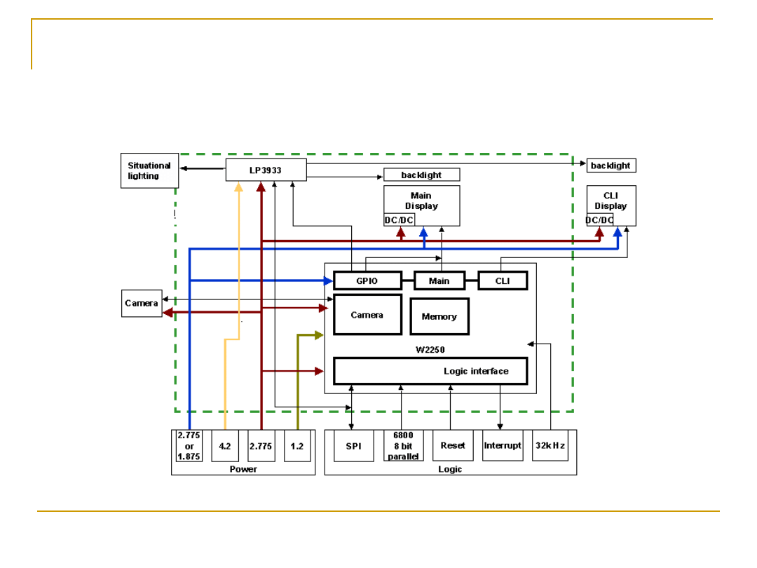
Flip Block Diagram

20
Motorola Confidential Proprietary
Camera
On camera: from hardware perspective, if they can open the flip and probe the 20-pin zif
connector on the display module, while the camera is connected verify following:
First place the camera in view finder mode either through UI or using test command and check
following signals:
B+ = 2.775 Vdc on pin 2.
Check input clock from ATI chip on pin 19, Clock freq ~ 13 - 14 MHz
Check output clock to ATI on pin 18. Should be same as input clock
Check control signals logic level. Both PD (pin 12) and RS (pin 13) should be logic low
below ~).7 Vdc
Check on oscilloscope that D0 - D7, data lines (pin 4 - 11), are randomly toggling during
viewfinder
Check periodic synch signals, HS (pin 16) and VS (pin 15) on oscilloscope. They should
have periodic format during viewfinder.
Check I2C lines SDA (pin 14) and SCL (pin 17). When a test command or any command
sent to the camera it goes over this 2-pin bus and make sure that lines are toggling
upon command sent.
If any of the above is too complicated and time consuming then take the camera out place new
camera and see it works.
If that does not work then replace the display module.
If that does not work, then get a new phone!
Document Outline
- Triplets Baseband Overview
- Regulators
- PCAP Regulators Sequencing
- Charger
- Charger –Cont’d
- Slide 6
- Slide 7
- RX Audio
- TX Audio
- PCAP
- Neptune LTE (U800)
- Slide 12
- 26 MHz Clock, Y805
- Flash/SRAM Memory, U700
- Slide 15
- Bluetooth System Block
- Bluetooth
- Flip LCD Modules
- Flip Block Diagram
- Camera
Wyszukiwarka
Podobne podstrony:
Training SLides
V80 TX Training slides
Positron emission tomography slides
1997 biofeedback relax training and cogn behav modif as treatment QJM
10 Principles of Marathon Training
CATIA V5 Training Basics
L G LCD TV training manual ML024 v
general training reading answers 6 10
IELTS1 gen training
SHSBC108 TRAINING DUPLICATION
Pytania i odpowiedzi ? 5 ISM CODE Training
SAP?sis Training II
DC Training, by?
jj slides tex
credit slides 1
Breakthrough Training in the Zone cover
CCNA M4 CCNA Skills Assessment Student Training Exam
więcej podobnych podstron