DUAL FULL-BRIDGE PWM MOTOR DRIVER
Data Sheet
29319.28†
A3964SLB
Designed for pulse-width modulated (PWM) current control of bipolar
stepper motors, the A3964SB and A3964SLB are capable of continuous
output currents to
±800 mA and operating voltages to 30 V. Internal fixed
off-time PWM current-control circuitry can be used to regulate the maximum
load current to a desired value. An internal precision voltage reference is
provided to improve motor peak-current control accuracy. The peak load
current limit is set by the user’s selection of an external resistor divider and
current-sensing resistors.
The fixed off-time pulse duration is set by user-selected external RC
timing networks. The capacitor in the RC timing network also determines a
user-selectable blanking window that prevents false triggering of the PWM
current control circuitry during switching transitions. This eliminates the
need for two external RC filter networks on the current-sensing comparator
inputs.
For each bridge the PHASE input controls load current polarity by
selecting the appropriate source and sink driver pair. For each bridge the
ENABLE input, when held high, disables the output drivers. Special power-
up sequencing is not required. Internal circuit protection includes thermal
shutdown with hysteresis, transient-suppression diodes, and crossover-current
protection.
The A3964SB is supplied in a 24-pin plastic DIP with copper heat sink
tabs; A3964SLB is supplied in a 20-lead plastic SOIC with copper heat sink
tabs. The power tabs are at ground potential and need no electrical isolation.
FEATURES
■ ±800 mA Continuous Output Current Rating
■ 30 V Output Voltage Rating
■ Internal PWM Current Control, Saturated Sink Drivers
■ Internally Generated, Precision 2.5 V Reference
■ Internal Transient-Suppression Diodes
■ Internal Thermal-Shutdown Circuitry
■ Crossover-Current Protection, UVLO Protection
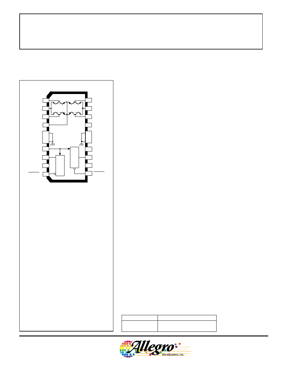
3964
1
V
BB
2
1
2
3
4
5
6
7
9
20
19
18
17
16
15
14
13
12
11
10
9
8
θ
2
θ
1
V
CC
PWM 1
PWM 2
GROUND
GROUND
GROUND
GROUND
PHASE
2
V
REF(OUT)
2
RC
1
RC
V
REF(IN)
PHASE
1
2B
OUT
SENSE
2
2A
OUT
1A
OUT
SENSE
1
1B
OUT
LOAD
SUPPLY
LOGIC
SUPPLY
Dwg. PP-047-1
ENABLE
1
ENABLE
2
Always order by complete part number:
Part Number
Package
A3964SB
24-Pin DIP
A3964SLB
20-Lead Wide-Body SOIC
ABSOLUTE MAXIMUM RATINGS
Load Supply Voltage, V
BB
. . . . . . . . . 33 V
Output Current, I
OUT
(10
µs) . . . . . .
±
1.0 A*
(continuous) . . . . . . . . . . . . .
±
800 mA*
Logic Supply Voltage, V
CC
. . . . . . . . . 7.0 V
Logic Input Voltage Range,
V
IN
. . . . . . . . . . . -0.3 V to V
CC
+ 0.3 V
Sense Voltage, V
S
. . . . . . . . . . . . . . . 1.0 V
Reference Output Current,
I
REF(OUT)
. . . . . . . . . . . . . . . . . . 1.0 mA
Package Power Dissipation,
P
D
. . . . . . . . . . . . . . . . . . . . See Graph
Operating Temperature Range,
T
A
. . . . . . . . . . . . . . . . -20˚C to +85˚C
Junction Temperature, T
J
. . . . . . . +150˚C†
Storage Temperature Range,
T
S
. . . . . . . . . . . . . . . -55˚C to +150˚C
* Output current rating may be limited by duty cycle,
ambient temperature, and heat sinking. Under any set
of conditions, do not exceed the specified current rating
or a junction temperature of 150˚C.
† Fault conditions that produce excessive junction
temperature will activate the device’s thermal shutdown
circuitry. These conditions can be tolerated but should
be avoided.
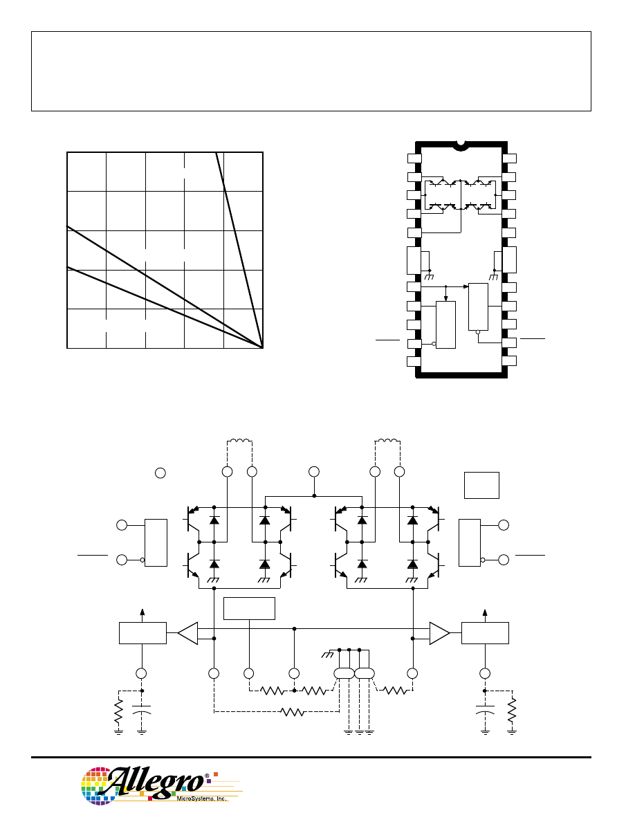
3964
DUAL FULL-BRIDGE
PWM MOTOR DRIVER
115 Northeast Cutoff, Box 15036
Worcester, Massachusetts 01615-0036 (508) 853-5000
2
A3964SB
1
2
3
4
5
6
7
8
9
24
23
22
21
20
19
18
17
16
15
14
13
12
11
10
9
θ
2
θ
1
V
CC
PWM 1
PWM 2
1
V
BB
2
GROUND
GROUND
GROUND
GROUND
PHASE
2
V
REF(OUT)
2
RC
2B
OUT
SENSE
2
2A
OUT
LOGIC
SUPPLY
Dwg. PP-005-2
NO
CONNECT.
NO
CONNECT.
ENABLE
2
1
RC
V
REF(IN)
PHASE
1
1A
OUT
SENSE
1
1B
OUT
LOAD
SUPPLY
NO
CONNECT.
NO
CONNECT.
ENABLE
1
NC
NC
NC
NC
50
75
100
125
150
5
1
0
ALLOWABLE PACKAGE POWER DISSIPATION IN WATTS
TEMPERATURE IN
°C
4
3
2
25
Dwg. GP-049-4
R = 6.0
°C/W
θJT
SUFFIX 'B', R = 40
°C/W
θJA
SUFFIX 'LB', R = 60
°C/W
θJA
2.5 V
REFERENCE
14
5
2
R S
19
R S
V
REF(IN)
V
CC
OUT
1A
OUT
1B
OUT
2A
OUT
2B
SENSE
1
SENSE
2
LOGIC
SUPPLY
LOAD
SUPPLY
ENABLE1
ENABLE2
RC
1
RC
2
PHASE 1
PHASE 2
V
BB
1
–
+
ONE SHOT
SOURCE
DISABLE
–
+
SOURCE
DISABLE
2
ONE SHOT
PWM 1
PWM 2
UVLO
& TSD
8
10
9
3
1
4
18
20
7
12
11
13
17
R T
R T
C T
C T
Dwg. FP-033-1
REF
OUT
REF
IN
6 15 16
R A
R B
FUNCTIONAL BLOCK DIAGRAM
(A3964SLB pinning shown)
Copyright © 1997, 2000 Allegro MicroSystems, Inc.

3964
DUAL FULL-BRIDGE
PWM MOTOR DRIVER
www.allegromicro.com
3
NOTES: 1. Typical Data is for design information only.
2. Negative current is defined as coming out of (sourcing) the specified device terminal.
TRUTH TABLE
ENABLE
PHASE
OUT
A
OUT
B
H
X
Off
Off
L
H
H
L
L
L
L
H
ELECTRICAL CHARACTERISTICS at T
A
= +25
°
C, V
BB
= 30 V, V
CC
= 4.75 V to 5.25 V,
V
S
= 0 V, 30 k
Ω
& 1000 pF RC to Ground (unless noted otherwise)
Limits
Characteristic
Symbol
Test Conditions
Min.
Typ.
Max.
Units
Load Supply Voltage Range
V
BB
Operating, I
OUT
=
±800 mA, L = 3 mH
5.0
—
30
V
Output Sustaining Voltage
V
CE(sus)
I
OUT
=
±800 mA, L = 3 mH, V
BB
= 33 V
33
—
—
V
Output Leakage Current
I
CEX
V
OUT
= V
BB
= 33 V
—
<1.0
50
µA
V
OUT
= 0 V, V
BB
= 33 V
—
<1.0
-50
µA
Output Saturation Voltage
V
CE(SAT)
Source Driver, I
OUT
= -500 mA
—
1.0
1.2
V
Source Driver, I
OUT
= -750 mA
—
1.1
1.5
V
Source Driver, I
OUT
= -800 mA
—
—
1.7
V
Sink Driver, I
OUT
= +500 mA
—
0.3
0.6
V
Sink Driver, I
OUT
= +750 mA
—
0.5
1.2
V
Sink Driver, I
OUT
= +800 mA
—
—
1.5
V
Clamp Diode Forward Voltage
V
F
I
F
= 500 mA
—
1.1
1.4
V
(Sink or Source)
I
F
= 750 mA
—
1.3
1.6
V
I
F
= 800 mA
—
—
1.7
V
Motor Supply Current
I
BB(ON)
V
ENABLE
= 0.8 V
—
2.0
4.0
mA
(No Load)
I
BB(OFF)
V
ENABLE
= 2.4 V
—
0
500
µA
Output Drivers
X = Irrelevant

3964
DUAL FULL-BRIDGE
PWM MOTOR DRIVER
115 Northeast Cutoff, Box 15036
Worcester, Massachusetts 01615-0036 (508) 853-5000
4
Logic Supply Voltage Range
V
CC
Operating
4.75
—
5.25
V
Logic Input Voltage
V
IN(1)
2.4
—
—
V
V
IN(0)
—
—
0.8
V
Logic Input Current
I
IN(1)
V
IN
= 2.4 V
—
<1.0
20
µA
I
IN(0)
V
IN
= 0.8 V
—
<-2.0
-200
µA
Reference Output Voltage
V
REF(OUT)
V
CC
= 5.0 V, I
REF(OUT)
= 90 to 900
µA
2.45
2.50
2.55
V
Reference Output Current
I
REF(OUT)
3 k
Ω ≤ R
D
= R
A
+ R
B
≤ 15 kΩ
150
—
900
µA
Ref. Input Offset Current
I
OS
V
REF(IN)
= 1 V
-2.5
0
1.0
µA
Comparator Input Offset Volt.
V
IO
V
REF(IN)
= 0 V
-6.0
0
6.0
mV
Comparator Input Volt. Range
V
REF
Operating
-0.3
—
1.0
V
PWM RC Fixed Off-time
t
OFF RC
C
T
= 1000 pF, R
T
= 30 k
Ω
27
30
33
µs
PWM Propagation Delay Time
t
PWM
Comparator Trip to Source Off
—
1.2
2.0
µs
PWM Minimum On Time
t
ON(min)
C
T
= 1000 pF, R
T
≥
15 k
Ω, V
CC
= 5 V
—
2.5
3.6
µs
Propagation Delay Times
t
pd
I
OUT
=
±800 mA, 50% to 90%:
ENABLE On to Source On
—
3.2
—
µs
ENABLE Off to Source Off
—
1.2
—
µs
ENABLE On to Sink On
—
3.2
—
µs
ENABLE Off to Sink Off
—
0.7
—
µs
PHASE Change to Sink On
—
3.2
—
µs
PHASE Change to Source On
—
3.2
—
µs
PHASE Change to Sink Off
—
0.7
—
µs
PHASE Change to Source Off
—
1.2
—
µs
Thermal Shutdown Temp.
T
J
—
165
—
°C
Thermal Shutdown Hysteresis
∆T
J
—
15
—
°C
UVLO Disable Threshold
Decreasing V
CC
4.20
4.40
4.65
V
UVLO Hysteresis
UVLO Enable Volt. - UVLO Disable Volt.
0.075
0.125
0.175
V
UVLO Enable Threshold
Increasing V
CC
4.375
4.525
4.725
V
Logic Supply Current
I
CC(ON)
V
ENABLE 1
= V
ENABLE 2
= 0.8 V
—
60
85
mA
I
CC(OFF)
V
ENABLE 1
= V
ENABLE 2
= 2.4 V
—
13
17
mA
Logic Supply Current
∆I
CC(ON)
V
ENABLE 1
=
V
ENABLE 2
= 0.8 V
—
0.18
—
mA/
°C
Temperature Coefficient
Limits
Characteristic
Symbol
Test Conditions
Min.
Typ.
Max.
Units
ELECTRICAL CHARACTERISTICS at T
A
= +25
°
C, V
BB
= 30 V, V
CC
= 4.75 V to 5.25 V,
V
SENSE
= 0 V, 30 k
Ω
& 1000 pF RC to Ground (unless noted otherwise) (cont.)
NOTES: 1. Typical Data is for design information only.
2. Negative current is defined as coming out of (sourcing) the specified device terminal.
Control Logic

3964
DUAL FULL-BRIDGE
PWM MOTOR DRIVER
www.allegromicro.com
5
[(V
BB
– V
SAT(SOURCE+SINK)
) x t
ON(min)
max] – [1.05 (V
SAT(SINK)
+ V
F
) x t
OFF
]
1.05 (t
ON(min)
max + t
OFF
) x R
LOAD
I
AVG
≈
Internal PWM Current Control. The A3964SB and
A3964SLB contain a fixed off-time pulse-width modulated
(PWM) current-control circuit that can be used to limit the
load current to a desired value. The peak value of the
current limiting (I
TRIP
) is set by the selection of an external
current-sensing resistor (R
S
) and reference input voltage
(V
REF(IN)
). The internal circuitry compares the voltage
across the external sense resistor to the voltage on the
reference input terminal (V
REF(IN)
) resulting in a
transconductance function approximated by:
The reference input voltage is typically set with a
resistor divider from V
REF(OUT)
. To ensure proper operation
of the voltage reference, the resistor divider should have
an impedance of 3 k
Ω to 15 kΩ (R
D
= R
A
+R
B
). Within this
range, a low impedance will minimize the effect of the REF
IN input offset current.
The current-control circuitry limits the load current as
follows: when the load current reaches I
TRIP
, the compara-
tor resets a latch that turns off the selected source driver.
The load inductance causes the current to recirculate
through the sink driver and flyback diode.
For each bridge, the user selects an external resistor
(R
T
) and capacitor (C
T
) to determine the time period
(t
OFF
= R
T
C
T
) during which the source driver remains
disabled (see “RC Fixed Off-time” below). The range of
recommended values for C
T
and R
T
are 1000 pF to 1500
pF and 15 k
Ω to 100 kΩ respectively. For optimal load
current regulation, C
T
is normally set to 1000 pF (see
“Load Current Regulation” below). At the end of the RC
interval, the source driver is enabled allowing the load
current to increase again. The PWM cycle repeats,
maintaining the peak load current at the desired value.
RC Blanking. In addition to determining the fixed off-time
of the PWM control circuit, the C
T
component sets the
comparator blanking time. This function blanks the output
of the comparator when the outputs are switched by the
internal current-control circuitry (or by the PHASE or
ENABLE inputs). The comparator output is blanked to
I
TRIP
≈
V
REF(IN)
R
S
prevent false over-current detections due to reverse-
recovery currents of the clamp diodes, and/or switching
transients related to distributed capacitance in the load.
During internal PWM operation, at the end of the t
OFF
time, the comparator’s output is blanked and C
T
begins to
be charged from approximately 1.1 volts by an internal
current source of approximately 1 mA. The comparator
output remains blanked until the voltage on C
T
reaches
approximately 3 volts.
When a transition of the PHASE input occurs, C
T
is discharged to near ground during the crossover delay
time (the crossover delay time is present to prevent
simultaneous conduction of the source and sink drivers).
After the crossover delay, C
T
is charged by an internal
current source of approximately 1 mA. The comparator
output remains blanked until the voltage on C
T
reaches
approximately 3 volts.
When the device is disabled, via the ENABLE input,
C
T
is discharged to near ground. When the device is
re-enabled, C
T
is charged by an internal current source of
approximately 1 mA. The comparator output remains
blanked until the voltage on C
T
reaches approximately
3 volts.
The minimum recommended value for C
T
is
1000 pF. This value ensures that the blanking time is
sufficient to avoid false trips of the comparator under
normal operating conditions. For optimal regulation of the
load current, the above value for C
T
is recommended and
the value of R
T
can be sized to determine t
OFF
. For more
information regarding load current regulation, see below.
Load Current Regulation. Because the device operates
in a slow current-decay mode (2-quadrant PWM mode),
there is a limit to the lowest level that the PWM current
control circuitry can regulate load current. The limitation is
due to the minimum PWM duty cycle, which is a function of
the user-selected value of t
OFF
and the minimum on-time
pulse t
ON(min)
max that occurs each time the PWM latch is
reset. If the motor is not rotating, as in the case of a
stepper motor in hold/detent mode, a brush dc motor when
stalled or at startup, the worst case value of current
regulation can be approximated by:
FUNCTIONAL DESCRIPTION

3964
DUAL FULL-BRIDGE
PWM MOTOR DRIVER
115 Northeast Cutoff, Box 15036
Worcester, Massachusetts 01615-0036 (508) 853-5000
6
dc servo motor applications as the transfer function
between the duty cycle on the PHASE input and the
average voltage applied to the motor is more linear than in
the case of ENABLE PWM control (which produces a
discontinuous current at low current levels).
Miscellaneous Information. An internally generated
dead time prevents crossover currents that can occur
when switching phase.
Thermal protection circuitry turns off all drivers should
the junction temperature reach +165
°C (typical). This is
intended only to protect the device from failures due to
excessive junction temperatures and should not imply that
output short circuits are permitted. The hysteresis of the
thermal shutdown circuit is approximately 15
°C.
APPLICATION NOTES
Current Sensing. The actual peak load current (I
PEAK
) will
be above the calculated value of I
TRIP
due to delays in the
turn off of the drivers. The amount of overshoot can be
approximated by:
where V
BB
is the motor supply voltage, V
BEMF
is the back-
EMF voltage of the load, R
LOAD
and L
LOAD
are the resis-
tance and inductance of the load respectively, and t
PWM
is
specified in the electrical characteristics table.
To minimize current sensing inaccuracies caused by
ground trace IR drops, each current-sensing resistor
should have a separate return to the ground terminal of the
device. For low-value sense resistors, the IR drops in the
PCB can be significant and should be taken into account.
The use of sockets should be avoided as their contact
resistance can cause variations in the effective value of
R
S
.
Generally, larger values of R
S
reduce the aforemen-
tioned effects but can result in excessive heating and
power loss in the sense resistor. The selected value of R
S
should not cause the absolute maximum voltage rating of
1.0 V, for the SENSE terminal, to be exceeded. The
recommended value of R
S
is in the range of:
where t
OFF
= R
T
C
T
, R
LOAD
is the series resistance of the
load, V
BB
is the motor supply voltage and t
ON(min)
max
is
specified in the electrical characteristics table. When the
motor is rotating, the back EMF generated will influence
the above relationship. For brush dc motor applications,
the current regulation is improved. For stepper motor
applications when the motor is rotating, the effect is
dependent on the polarity and magnitude of the motor’s
back EMF.
The following procedure can be used to evaluate the
worst case internal PWM load current regulation in the
system:
Set V
REF(IN)
to 0 volts. With the load connected and the
PWM current control operating in slow decay mode, use
an oscilloscope to measure the time the output is low
(sink on) for the output that is chopping. This is the
typical minimum on time (t
ON(min)
typ) for the device. The
C
T
then should be increased until the measured value of
t
ON(min)
is equal to t
ON(min)
max as specified in the electri-
cal characteristics table. When the new value of C
T
has
been set, the value of R
T
should be decreased so the
value for t
OFF
= R
T
C
T
(with the artificially increased value
of C
T
) is equal to the nominal design value. The worst-
case load-current regulation then can be measured in
the system under operating conditions.
PWM of the Phase and Enable Inputs. The PHASE and
ENABLE inputs can be pulse width modulated to regulate
load current. Typical propagation delays from the PHASE
and ENABLE inputs to transitions of the power outputs are
specified in the electrical characteristics table. If the
internal PWM current control is used, the comparator
blanking function is active during phase and enable
transitions. This eliminates false tripping of the over-
current comparator caused by switching transients
(see “RC Blanking” above).
Enable PWM. Toggling the ENABLE input turns on and
off the selected source and sink drivers. The correspond-
ing pair of flyback and ground clamp diodes conduct after
the drivers are disabled, resulting in fast current decay.
When the device is enabled the internal current control
circuitry will be active and can be used to limit the load
current in a slow current-decay mode.
Phase PWM. Toggling the PHASE terminal selects which
sink/source pair is enabled, producing a load current that
varies with the duty cycle and remains continuous at all
times. This can have added benefits in bidirectional brush
(V
BB
– [(I
TRIP
x R
LOAD
) + V
BEMF
]) x t
PWM
L
LOAD
I
OS
≈
0.5
I
TRIP
max
R
S
≈
± 50%

3964
DUAL FULL-BRIDGE
PWM MOTOR DRIVER
www.allegromicro.com
7
If desired, the reference input voltage can be filtered
by placing a capacitor from REF
IN
to ground. The ground
return for this capacitor as well as R
B
should be indepen-
dent from the high-current power-ground trace to avoid
changes in REF
IN
due to IR drops.
Thermal Considerations. For reliable operation, it is
recommended that the maximum junction temperature be
kept below 110
°C to 125°C. The junction temperature can
be measured best by attaching a thermocouple to the
power tab/batwing of the device and measuring the tab
temperature, T
TAB
. The junction temperature can then be
approximated by using the formula:
T
J
≈ T
TAB
+ (2 I
LOAD
V
F
R
θJT
)
where V
F
can be chosen from the electrical specification
table for the given level of I
LOAD
. The value for R
θJT
is
approximately 6
°C/W for both package styles.
The power dissipation of the batwing packages can be
improved by 20 to 30% by adding a section of printed
circuit board copper (typically 6 to 18 square centimeters)
connected to the batwing terminals of the device.
The thermal performance in applications that run at
high load currents and/or high duty cycles can be im-
proved by adding external diodes from each output to
ground in parallel with the internal diodes. Fast-recovery
(
≤200 ns) diodes should be used to minimize switching
losses.
The load supply terminal, V
BB
, should be decoupled
with an electrolytic capacitor (
≥47 µF is recommended)
placed as close to the device as is physically practical.
To minimize the effect of system ground IR drops on the
logic and reference input signals the system ground should
have a low-resistance return to the load supply voltage.
See also “Current Sensing” and “Thermal Consider-
ations” above.
Fixed Off-Time Selection. With increasing values of t
OFF
,
switching losses will decrease, low-level load current
regulation will improve, EMI will be reduced, the PWM
frequency will decrease, and ripple current will increase.
The value of t
OFF
can be chosen for optimization of these
parameters. For applications where audible noise is a
concern, typical values of t
OFF
are chosen to be in the
range of 15 to 35
µs.
The products described here are manufactured under one or more
U.S. patents or U.S. patents pending.
Allegro MicroSystems, Inc. reserves the right to make, from time to
time, such departures from the detail specifications as may be required
to permit improvements in the performance, reliability, or
manufacturability of its products. Before placing an order, the user is
cautioned to verify that the information being relied upon is current.
Allegro products are not authorized for use as critical components
in life-support devices or systems without express written approval.
The information included herein is believed to be accurate and
reliable. However, Allegro MicroSystems, Inc. assumes no responsi-
bility for its use; nor for any infringement of patents or other rights of
third parties which may result from its use.
3964
DUAL FULL-BRIDGE
PWM MOTOR DRIVER
115 Northeast Cutoff, Box 15036
Worcester, Massachusetts 01615-0036 (508) 853-5000
8
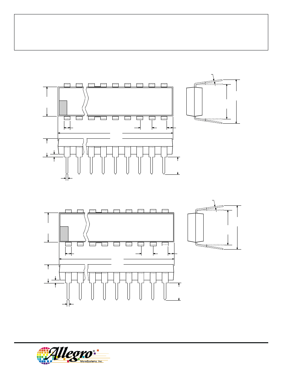
NOTES: 1.
Webbed lead frame. Leads 6, 7, 18, and 19 are internally one piece.
2.
Lead spacing tolerance is non-cumulative.
3.
Exact body and lead configuration at vendor’s option within limits shown.
4.
Lead thickness is measured at seating plane or below.
5.
Supplied in standard sticks/tubes of 15 devices.
0.355
0.204
7.62
BSC
Dwg. MA-001-25A mm
10.92
MAX
24
1
12
7.11
6.10
5.33
MAX
1.77
1.15
0.39
MIN
0.558
0.356
2.54
BSC
0.13
MIN
3.81
2.93
13
32.51
31.24
NOTE 1
6
7
A3964SB
Dimensions in Inches
(controlling dimensions)
Dimensions in Millimeters
(for reference only)
0.014
0.008
0.300
BSC
Dwg. MA-001-25A in
0.430
MAX
24
1
6
12
0.280
0.240
0.210
MAX
0.070
0.045
0.015
MIN
0.022
0.014
0.100
BSC
0.005
MIN
0.150
0.115
13
1.280
1.230
NOTE 1
7
3964
DUAL FULL-BRIDGE
PWM MOTOR DRIVER
www.allegromicro.com
9
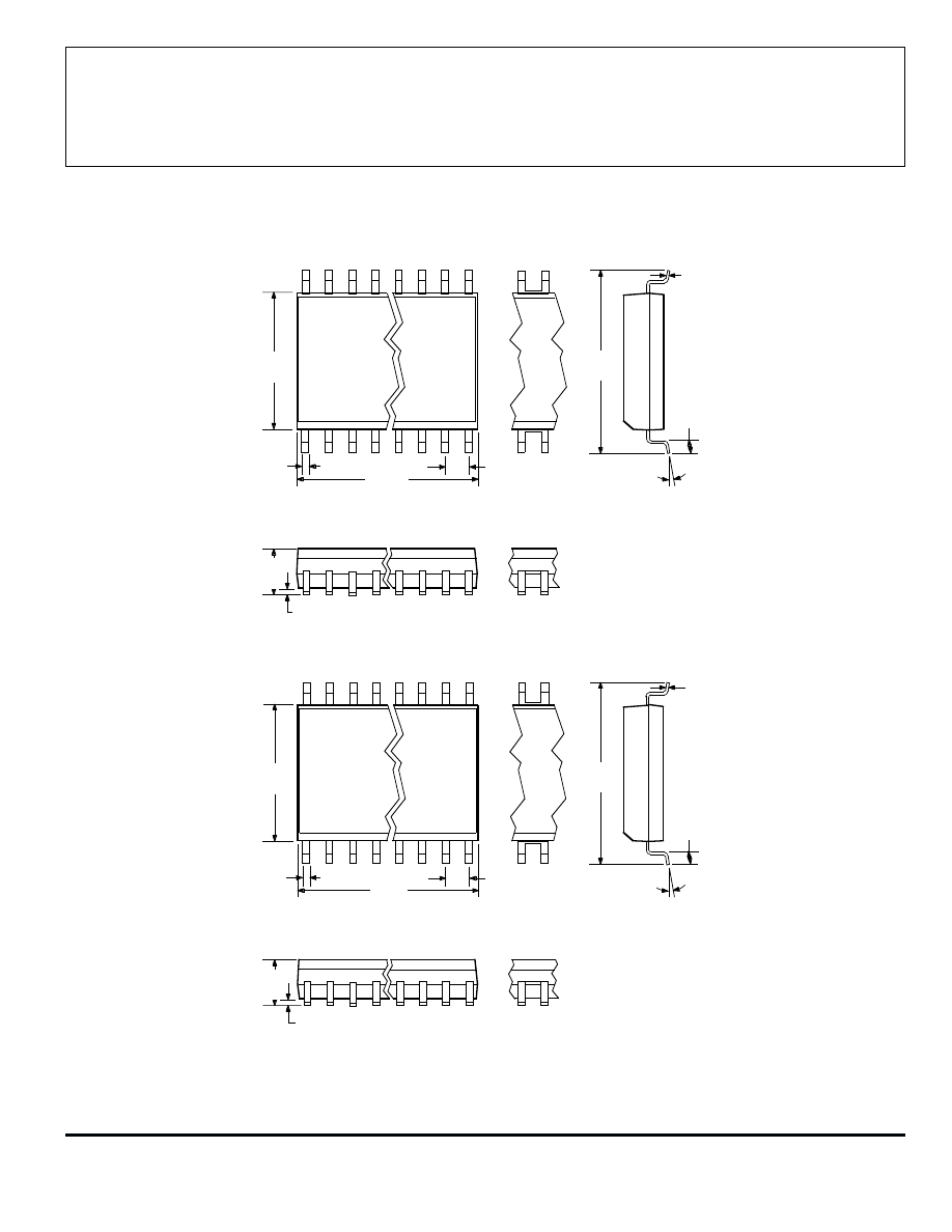
NOTES: 1.
Webbed lead frame. Leads 5, 6, 15, and 16 are internally one piece.
2.
Lead spacing tolerance is non-cumulative.
3.
Exact body and lead configuration at vendor’s option within limits shown.
4.
Supplied in standard sticks/tubes of 37 devices or add “TR” to part number for tape and reel.
0
°
TO
8
°
1
2
3
0.020
0.013
0.0040
MIN.
0.0125
0.0091
0.050
0.016
Dwg. MA-008-21A in
0.050
BSC
20
11
NOTE 1
NOTE 3
0.2992
0.2914
0.419
0.394
0.5118
0.4961
0.0926
0.1043
0
°
TO
8
°
1
20
2
3
0.51
0.33
0.10
MIN.
Dwg. MA-008-21A mm
1.27
BSC
11
0.32
0.23
1.27
0.40
NOTE 1
NOTE 3
7.60
7.40
10.65
10.00
13.00
12.60
2.65
2.35
A3964SLB
Dimensions in Inches
(for reference only)
Dimensions in Millimeters
(controlling dimensions)

3964
DUAL FULL-BRIDGE
PWM MOTOR DRIVER
115 Northeast Cutoff, Box 15036
Worcester, Massachusetts 01615-0036 (508) 853-5000
10
MOTOR DRIVERS
Function
Output Ratings*
Part Number
†
INTEGRATED CIRCUITS FOR BRUSHLESS DC MOTORS
3-Phase Power MOSFET Controller
—
28 V
3933
3-Phase Power MOSFET Controller
—
50 V
3932
3-Phase Power MOSFET Controller
—
50 V
7600
2-Phase Hall-Effect Sensor/Driver
400 mA
26 V
3626
Bidirectional 3-Phase Back-EMF Controller/Driver
±600 mA
14 V
8906
2-Phase Hall-Effect Sensor/Driver
900 mA
14 V
3625
3-Phase Back-EMF Controller/Driver
±900 mA
14 V
8902–A
3-Phase Controller/Drivers
±2.0 A
45 V
2936 & 2936-120
INTEGRATED BRIDGE DRIVERS FOR DC AND BIPOLAR STEPPER MOTORS
Dual Full Bridge with Protection & Diagnostics
±500 mA
30 V
3976
PWM Current-Controlled Dual Full Bridge
±650 mA
30 V
3966
PWM Current-Controlled Dual Full Bridge
±650 mA
30 V
3968
PWM Current-Controlled Dual Full Bridge
±750 mA
45 V
2916
PWM Current-Controlled Dual Full Bridge
±750 mA
45 V
2919
PWM Current-Controlled Dual Full Bridge
±750 mA
45 V
6219
PWM Current-Controlled Dual Full Bridge
±800 mA
33 V
3964
PWM Current-Controlled Full Bridge
±1.3 A
50 V
3953
PWM Current-Controlled Dual Full Bridge
±1.5 A
45 V
2917
PWM Current-Controlled Microstepping Full Bridge
±1.5 A
50 V
3955
PWM Current-Controlled Microstepping Full Bridge
±1.5 A
50 V
3957
PWM Current-Controlled Dual DMOS Full Bridge
±1.5 A
50 V
3972
Dual Full-Bridge Driver
±2.0 A
50 V
2998
PWM Current-Controlled Full Bridge
±2.0 A
50 V
3952
DMOS Full Bridge PWM Driver
±2.0 A
50 V
3958
Dual DMOS Full Bridge
±2.5 A
50 V
3971
UNIPOLAR STEPPER MOTOR & OTHER DRIVERS
Voice-Coil Motor Driver
±500 mA
6 V
8932–A
Voice-Coil Motor Driver
±800 mA
16 V
8958
Unipolar Stepper-Motor Quad Drivers
1 A
46 V
7024 & 7029
Unipolar Microstepper-Motor Quad Driver
1.2 A
46 V
7042
Unipolar Stepper-Motor Translator/Driver
1.25 A
50 V
5804
Unipolar Stepper-Motor Quad Driver
1.8 A
50 V
2540
Unipolar Stepper-Motor Quad Driver
1.8 A
50 V
2544
Unipolar Stepper-Motor Quad Driver
3 A
46 V
7026
Unipolar Microstepper-Motor Quad Driver
3 A
46 V
7044
* Current is maximum specified test condition, voltage is maximum rating. See specification for sustaining voltage limits or
over-current protection voltage limits. Negative current is defined as coming out of (sourcing) the output.
† Complete part number includes additional characters to indicate operating temperature range and package style.
Also, see 3175, 3177, 3235, and 3275 Hall-effect sensors for use with brushless dc motors.
Wyszukiwarka
Podobne podstrony:
3964
3964
3964
3964
3964
3964
3964
3964
5 B 1800 r p n e 1572 r n Peru, Kolumbia, Ekwador id 3964 (2)
3964
3964 zamordowanych ludzi w UE przez eksperymentalne szczepionki przeciw Covid
więcej podobnych podstron