
REV. 0
a
AN-557
APPLICATION NOTE
One Technology Way • P.O. Box 9106 • Norwood, MA 02062-9106 • 781/329-4700 • World Wide Web Site: http://www.analog.com
An Experimenter’s Project for Incorporating the AD9850 Complete-DDS Device as a
Digital LO Function in an Amateur Radio Transceiver*
PIC “N” MIX DIGITAL INJECTION SYSTEM
By Peter Rhodes, BSc, G3XJP (email pirrhodes@aol.com)
PART 1 OF 5
This construction project brings together a number of
themes which I have been kicking around for some time.
But first, why PIC “N” MIX?
TWO ESSENTIAL TERMS
PIC—A range of microcontrollers produced by Arizona
Microchip Inc. In this application, the PIC16C84.
DDS—Direct Digital Synthesis. The technique of digi-
tally generating the output frequency directly (as opposed
to typically mixing the output of a VFO with a crystal
oscillator—or employing phase-locked loop techniques).
In this application the Analog Devices AD9850 “com-
plete DDS synthesizer” chip is used.
IN BRIEF . . .
PIC “N” MIX provides PIC controlled direct generation
of the required injection frequencies into the signal fre-
quency mixer in your transceiver.
PIC “N” MIX also in the sense that you can pick and
choose which functional elements you build; and in
the sense that there are by design a number of differ-
ent mechanical configurations to best suit your
circumstances.
You are also presented with the radical choice of using
the software I have designed—or writing your own.
The PIC microcontroller (and about 400 hours of soft-
ware development) provides control and operational
flexibility while the DDS chip is used to synthesize the
RF output giving stability and low-phase noise.
CONVERGING THEMES
Discounting the value of your time, I would argue that
for years it has been viable to build multiband HF trans-
ceivers which outperform their commercial counter-
parts at any point on the price versus performance
graph—from the cheap and cheerful through to the truly
exotic. Except, that is, for one critical element—the
injection oscillator.
I have been building VFOs for years that for all practical
purposes didn’t drift. Almost all were based on the
Vackar running somewhere between 5 MHz–10 MHz.
Besides some time consuming temperature compensa-
tion, I never gave them a second thought.
But they need about eight x’tals, a mixer and switched
bandpass filters before they can feed both the signal fre-
quency mixer—and a frequency counter which gives a
natural display of exactly not quite the frequency you
are on! It can all be made to work, but only at substantial
cost in time, money and space. And the only incremen-
tal feature easily obtained is IRT.
Then in February 1996, Technical Topics reported the
results of some phase noise measurements made by
Colin Horrabin, G3SBI and Jack Hardcastle, G3JIR on a
stable Vackar as “rather disappointing.” This set me
thinking. Most of us ignore oscillator phase noise
because we can’t measure it. Myself included. Does it
really matter in practice?
The ARRL handbook has an excellent section on the
subject which concludes “. . . far-out phase noise can
significantly reduce the dynamic range of a receiver. Far-
out phase noise performance has effects just as critical as
blocking dynamic range and two-tone dynamic range
performance of receivers.” Yes, but does it really matter
in practice? I mean, am I truly going to fail to copy real
signals on a significant number of occasions because of
poor phase noise performance?
*This five-part article is reprinted in its entirety by permission of RadCom
Magazine, a ham radio magazine publication in the U.K.(website
www.rsgb.com), and the author. All international copyrights are reserved.

REV. 0
–2–
AN-557
I determined to find out by adopting the simple expedient
of fitting a changeover switch between my traditional
VFO and a phase-quiet alternative of the same power
output. Then, under a variety of practical conditions,
could I tell the difference? The problem, of course, was
to find this alternative without spending impracticable
sums of money.
Technical Topics came to the rescue again by first bring-
ing to my notice the Analog Devices AD9850 DDS chip.
A few minutes on the Internet produced the data sheet—
and it all looked too good to be true.
So, I set about designing some traditional TTL to control
it and actually got as far as building some of the boards
before giving up. Because although I have no doubt
it would have worked, 28 TTL chips to control one
DDS chip—and provide a modest range of useful
features—was ignoring any reasonable definition of the
“in practice” imperative.
It was obvious from the outset that some form of micro-
controller would provide the solution to the control
problem and at the same time offering the ability to
provide a range of operational features. What put me off
for months was the costs of acquiring the development
environment and the hardware to program the chip. A
glance in the larger catalogues suggested little change
from a £200 investment for PIC development—totally
unacceptable.
The bottom line is this. Arizona Microchip provide on
their website their complete development environment
at no cost—as well as copious application material. And
there are numerous circuits for PIC Programmers pub-
lished on the Internet which you can build for less than
£5. The project was born.
. . . AND THE CONCLUSION?
Phase noise does matter in practice. On a substantial
number of occasions it makes the difference between R2
and R5 on SSB signals.
For example, the home-brew net convenes daily around
lunch time on 80 m just down from the SSTV calling
frequency and just up from a prominent French coastal
station. A convenient source of large adjacent channel
signals.
If the band is flat and quiet, it makes no difference. If
conditions are lively—using the DDS source—then I can
often copy Ed, EI9GQ at only just R5. Switch over to the
VFO and the readability instantly degrades to near hope-
less if and only if there is significant adjacent channel
activity. The effect is insidious. Its not that Ed’s signal
goes down. Its that the base level of band background
noise appears to go up. It doesn’t of course.
What is happening is that the noise sidebands on my
VFO are mixing with adjacent signals to produce
incremental noise in the passband. A very salutary
experience because this noise is totally indistinguish-
able from band noise and you could operate for years
without realizing what was happening.
It would seem that there is a basic conflict in VFO
design. The traditional view is that you drive the oscilla-
tor gently to keep the heat (and, therefore, drift) down
and follow it with an appropriate buffer to get the power
up to the required level. This approach also maximizes
phase noise.
Conversely, if you drive it hard then it becomes increas-
ingly difficult (in my experience, next to impossible) to
maintain acceptable frequency stability.
With the DDS approach, phase noise and drift are
intrinsically small. The topic is covered shortly.
PIC “N” MIX SUMMARY
Before covering the essential theory these are the
features on offer should you adopt my software:
GENERAL SUMMARY
•
PIC “N” MIX replaces the functions of the crystal
oscillator bank, VFO, mixer, bandpass filters, power
driver and frequency counter associated with a con-
ventional HF transceiver with significantly enhanced
features and lower cost. Not merely a VFO!
•
Alternatively, it acts as a programmable and/or tunable
signal source with output from audio to 40 MHz in
10 Hz steps.
•
All functions are controlled by either a multifunction
tuning knob—or by a simple telephone keypad with
65 discrete key combinations recognized by the
software.
•
A large six-digit seven-segment display with auto-
ranging gives a resolution of 10 Hz.
•
Two independent VFOs provide IRT, ITT and cross-
band operation.
•
A variety of tuning and scanning modes provides
operational flexibility.
•
Any desired frequency may be entered directly from
the keypad.
•
The switch-on frequency and nine band initialization
frequencies are user programmable.
•
As are 10 frequency memories.
•
Any three IF offsets (USB, LSB and CW separately) in
the HF range may be entered.
•
USB/LSB/CW selection outputs—and band switching
outputs to the host transceiver are provided as a
hardware option.
–3–
AN-557
REV. 0
•
Front panel LEDs provide status information and
double as a bar-graph to show tuning rate.
•
Finally, there are a number of possible physical
layouts providing flexible outboard or integrated
configurations.
ADMINISTRATIVE FEATURES
•
The frequency accuracy is determined by a reference
oscillator in the VHF range. You may use any crystal
in the range 100 MHz–125 MHz and program the
actual frequency into the software yourself.
•
Final calibration and any subsequent correction for
crystal ageing are achieved using the tuning knob to
drive a trimmer in software. A physical trimmer
which would inevitably introduce drift and phase
noise is neither required nor provided.
•
IF offsets may be entered from the keypad and/or
trimmed to zero beat with the host transceiver carrier
crystals.
•
As an injection oscillator, the output frequency is the
selected IF frequency plus or minus the desired fre-
quency. The choice of high-side or low-side injection
may be made “on the fly” with the sideband selection
outputs to the host being switched to correspond.
OPERATIONAL FEATURES
•
Intelligent tuning continuously monitors the speed
and duration of tuning knob rotation to vary the tuning
rate dynamically. Thus the longer and faster you turn
the knob, the greater the tuning increments.
•
A software flywheel engages automatically at high
tuning speeds for rapid and/or large frequency
excursions—and is disengaged by the slightest turn
of the knob in the opposite direction.
•
As opposed to traditional tuning where rotation of
the knob alters frequency, a tuning rate option is pro-
vided whereby rotation of the knob alters the rate of
frequency change—from zero to very fast.
This is particularly useful for casually scanning around a
band without having to continuously turn the knob.
•
Guard channel operation provides normal tuning, but
with a brief switch to another chosen spot frequency
about every 20 seconds.
•
Up to ten memories may be programmed with
frequency. As opposed to merely providing spot
frequencies, they are also jumping off points for
further tuning.
•
Memory scanning mode cycles between the ten
memory frequencies at a speed determined by the
tuning knob.
•
Spot scanning switches between two chosen spot
frequencies at a speed determined by the tuning
knob.
•
Range scanning tunes up and down between two
chosen limits with frequency increments determined
by the tuning knob.
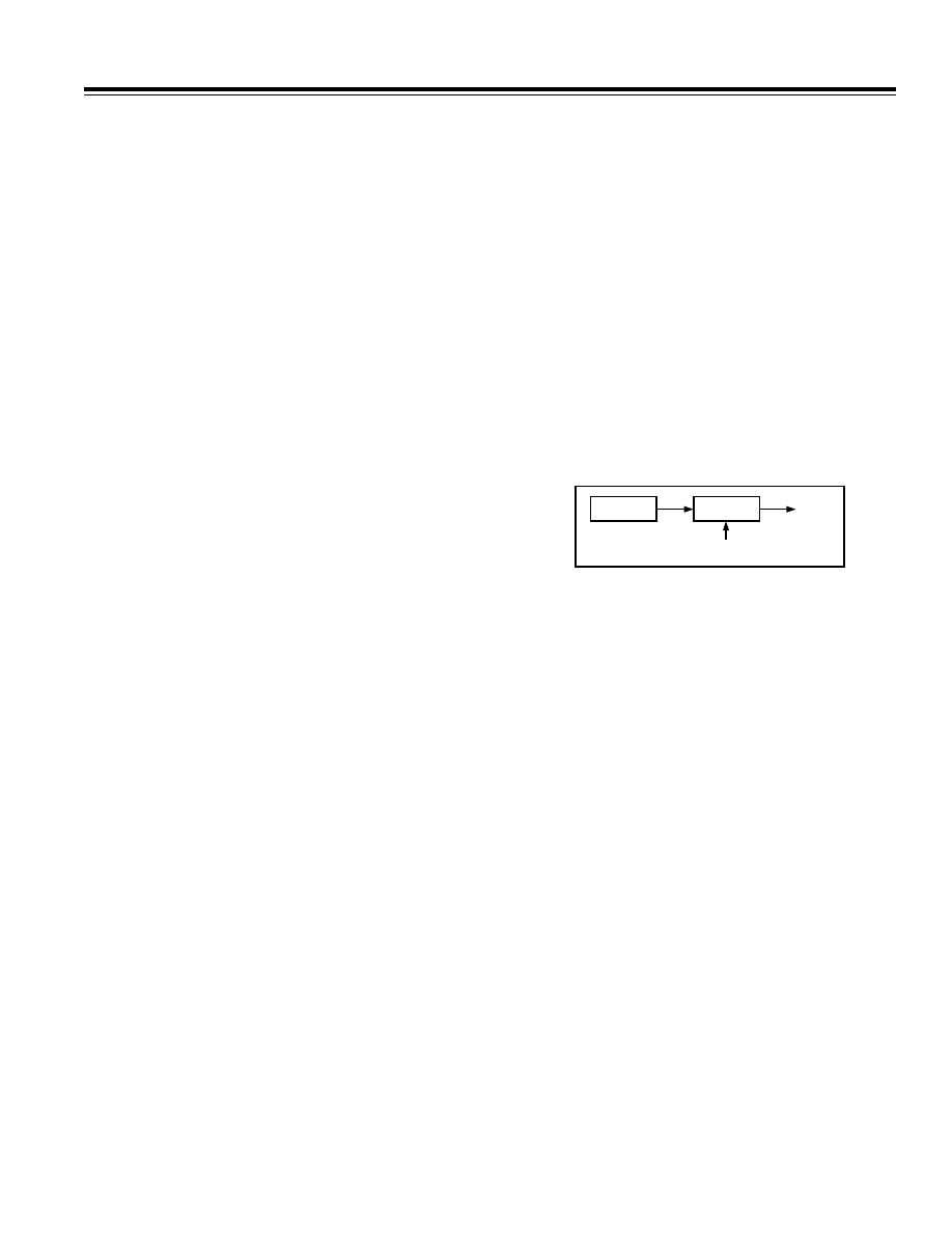
AD9850 DDS
Throughout this article, I have used the nomenclature
used by Analog Devices in their data sheet and only
mentioned the features and configuration of the chip
used in this project. There are others.
There is little you need to know about the internal workings
of this device. The most significant consideration is that
it contains the DAC—necessary to convert the digitally
generated sine wave to analogue form—on the chip. So
you neither have to worry about specifying a suitable
DAC nor interfacing it.
REFERENCE
CLOCK
AD9850
CLKIN
F
OUT
32-BIT TIMING WORD
(GENERATED BY PIC)
Figure 1. DDS Block Diagram
The basic block diagram is shown in Figure 1. There is a
simple relationship between the output frequency
FOUT, the reference clock frequency CLKIN, and the 32-
bit tuning word
∆Phase:
FOUT = (
∆
Phase
× CLKIN)/2
32
Using a 125 MHz clock, the highest frequency permitted,
this gives us tuning increments of 0.0291 Hz, orders of
magnitude better than needed for this application. In
practice this means that using 10 Hz tuning increments
an error of 0.0291 Hz is significantly smaller than, for
example, any drift on your carrier x’tal.
Stability in a DDS system is the same (in parts per
million) as that of the reference clock x’tal oscillator. For
example, if the 125 MHz clock drifts by 10 Hz then on
80 m with 12.5 MHz injection, you will drift by 1 Hz.
Phase noise on the DDS output is better than that of the
reference clock—which contributes most of the system
phase noise. The improvement is
20 log (
CLKIN/FOUT) dB
Is it that simple? Unfortunately, not quite, for as well as
generating the required frequency, aliased or image
outputs are also present. This is inherent in any sampled
signal and the output observes Nyquist’s theorem. The
aliased images are at multiples of the reference clock,
CLKIN
± the output frequency FOUT. Thus with a clock
frequency of 125 MHz and the wanted output at 20 MHz,
the images will be at 105 MHz (first image), 145 MHz
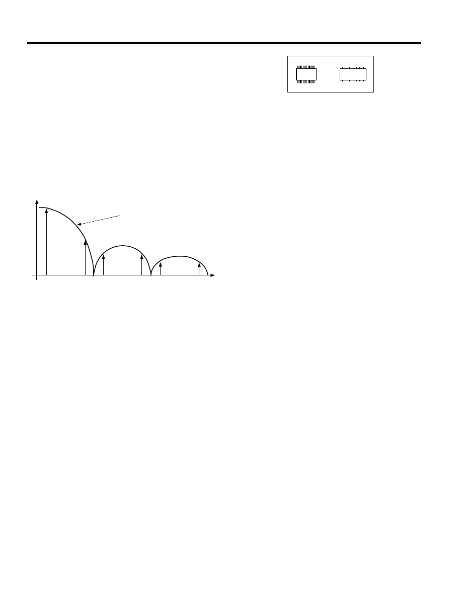
REV. 0
–4–
AN-557
(second image), 230 MHz (third image), 270 MHz (fourth
image) . . . and so on.
Another consequence of Nyquist’s theorem is that the
maximum theoretical output frequency is half the refer-
ence clock frequency—but in practice, one third is usually
taken as a rule-of-thumb limit—to provide a reasonable
separation between the wanted signal and significant
images.
The amplitude of the images follows a sine envelope as
shown in Figure 2. A low-pass filter is therefore inserted
in the output to reduce the image outputs; and on the
highest bands using a high IF, the Tx/Rx signal frequency
tuned circuits offer further protection. Using the highest
possible reference clock frequency obviously helps.
REFERENCE CLOCK CLKIN FREQUENCY – 125MHz
AMPLITUDE
SIN(X)/X ENVELOPE
WHERE X = (
) F
OUT
/CLKIN
FIRST
IMAGE
THIRD
IMAGE
FIFTH
IMAGE
SECOND
IMAGE
FOURTH
IMAGE
20
105
145
230
270
355
Figure 2. DDS Output Spectrum
There are other discrete AM spurious outputs as a result
of limitations in DAC technology. The significant ones
are few in number and appear from the user’s perspective
to be at random frequencies. Analog Devices specify
them as better than 50 dB down and the practical conse-
quence of these is an occasional birdie.
The remaining AM spurs form a continuous noise floor
at about 70 dB down and these give rise to the greatest
concern. A typical double balanced mixer will furnish
about 40 dB further suppression—so if the mixer is
injected at +7 dBm, weak birdies will be heard if the
band noise is less than 2 mV at the mixer RF port. On the
LF bands with most receivers this will be academic but
on, say, 10 m a typical Rx will need to use an RF preamp
with some 25 dB net gain to both retain adequate sensi-
tivity and to mask the noise floor. This topic will be
much less of an issue when 12-bit DDS is available at
affordable prices but meanwhile this 10-bit DDS may not
be suitable for all home-brew Rx topologies, particularly
if you are reluctant to alter your gain distribution.
The final challenge with the AD9850 is its size, see
Figure 3. Designed for surface mounting, it is truly
microscopic. Much effort has gone into finding repeatable
amateur methods of mounting it which do not com-
promise performance. Analog Devices recommend a
4-layer board with dedicated power and ground planes.
AD9850
14-PIN DIL
Figure 3. AD9850’s 28-Lead Shrink Small Outline
Package as Compared to a 14-Lead DIL Package
I tried it on double-sided board, both surface mounted
and let into a slot so that it sat in the thickness of the
PCB. I had no great problems hand-etching the boards—
but found substantial difficulty in soldering the chip to the
pads. The best I managed was with a medium-sized iron
and a length of sharpened copper wire bound to the bit—
and very fine solder. The propensity to bridge adjacent
leads was enormous. Worst, it seemed impossible to
maintain clean power and ground plane layouts— which
ultimately prejudices the phase-noise performance.
After obtaining a batch of 50 unmarked devices in the
same packaging at a rally and having destroyed many in
the quest, I settled on a dead-bug approach with con-
tinuous power and ground planes—mounted as a sub-
assembly on a DIL socket and with the input/output
leads taken out to the DIL socket on fine wires.
This method is reproducible if you have average eye-
sight (or a good magnifier) and a short-term steady
hand. The process is described in detail in Part 2 of
this article.
THE WORLD OF PICS
THE 16C84 IS ONE of a large and growing range of 8-bit
microcontrollers. The devices vary according to speed,
the amount of memory, built in devices (including A-D
converters) and other features. For the latest detail, con-
sult the Arizona Microchip website.
The 16C84 specifically is—in brief—an electrically
reprogrammable device with 1 k of program memory
(i.e., room for 1024 instructions), 36 bytes of working
data and 64 bytes of data EEPROM which survives
power down; and 13 input/output pins.
Also on the website you will find the integrated develop-
ment environment MPLAB which was used exclusively
in developing my software. It includes an editor, assem-
bler and simulator. The latter is particularly useful since
you can progressively build and test code with your target
chip simulated on the PC—no real hardware needed.
If you want to download MPLAB, watch your phone bill
because it is about 5 MB when unzipped!
You can run elements of the software under DOS, but
I used it exclusively under Windows. At first under
Windows 3.1 on a 386 and latterly under Windows ’95
on a 486. Both were entirely satisfactory. C++ compilers
are also available, but I haven’t tried any of them, all my
work being in assembler.

–5–
AN-557
REV. 0
Of the various programmers available, I built TOPIC by
David Tait
6
which runs out of the PC parallel port. You
can also build ones for serial port operation and some
even need no power supply, deriving their power from
the port.
Having conducted the intellectual exercise of “designing”
some aspect of the software, the mechanics are easy
enough. After typing in the code using the editor, you
assemble it and then run it on the simulator—if necessary
one instruction at a time—looking at intermediate and
end results to see if it works. You can also check execu-
tion times. When you are happy, you then download the
software onto the PIC using the programmer (say, 10
seconds) and run your code in the real world. If you are
careful, the PIC can be programmed in situ in the target
environment which speeds up the process enormously.
The assembler language itself is easy to learn with only
35 instructions. The art, it turns out, is usually not
whether you can write something that works but rather,
can you find an efficient enough way of doing it to
squeeze it into the space without unduly compromising
features, performance and ultimately maintainability?
As Eric Morecombe once said “Composing good music is
the same as composing bad music. Its just a matter of put-
ting the notes in a different order.” So it is with software!
So, if you have never written any software before and
have a PC with at least temporary access to the Internet,
you can have a go with no incremental cost. (Or you
could buy a suitable secondhand PC for about £50—and
most Internet service providers offer a free trial period.)
Think of the range of applications—self-tuning ATUs,
intelligent AGC generators, keyers and readers; in fact
any application involving control or logic is a potential
candidate where one 18-pin DIL coupled with your intel-
lect can replace acres of conventional hardwired logic at
trivial cost. Who says computers and amateur radio
don’t mix? In my view these microcontrollers are going
to dominate many aspects of home-brew construction
before long.
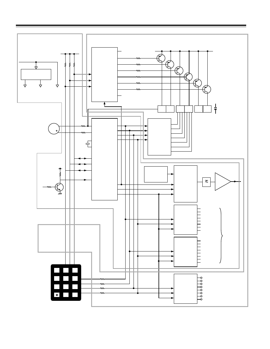
THE INPUT/OUTPUT CHALLENGE
AS JUST MENTIONED the 16C84 has 13 input/output (I/O)
pins for controlling its environment. How many are
actually needed? The following is the first-pass answer:
Inputs—total of 15 as follows:
PTT Line Monitoring . . . . . . . . . . . . . . . . . . . . . . . . . . . 1
Keypad 4
× 3 . . . . . . . . . . . . . . . . . . . . . . . . . . . . . . . . 12
Shaft Encoder . . . . . . . . . . . . . . . . . . . . . . . . . . . . . . . 2
Outputs—Total of 74 as follows:
6 Digits
× 7 Segments + Decimal . . . . . . . . . . . . . . . 48
Status LEDs . . . . . . . . . . . . . . . . . . . . . . . . . . . . . . . . . . 8
Band Switch Outputs . . . . . . . . . . . . . . . . . . . . . . . . . 15
AD9850 Control . . . . . . . . . . . . . . . . . . . . . . . . . . . . . . 3
Giving a grand total (apparently) of 89.
Clearly something has to give and some supplemental
hardware is needed. There is, however, one mitigating
feature. The 13 I/O pins on the PIC can be used as either
inputs or outputs—and you can change them “on the
fly” in midprogram so with cunning they can be both!
Firstly, the 12 keypad switches aren’t individually moni-
tored. Each row is tested in turn looking at each column
in turn for key presses. This needs only seven I/O lines.
Next, rather than drive each display separately, each
one is driven in turn—in rapid succession; i.e., they are
multiplexed. Two low-cost decoder chips are added and
this gets the I/O count for the display segments down to
seven. And of these, three outputs are in fact the same
lines as used for the three inputs for the keypad col-
umns; and the other four outputs are also multiplexed to
drive the keypad rows.
Then three serial in, parallel out latches are added to
handle status and band switching.
These have three unique data lines, a common clock line
(with all four again multiplexed with the display)—and a
latch line shared with the AD9850.
The final touch is to drive the decimal point output on
the same line as the shaft encoder direction input.
If you have kept up with this, then you will agree that the
total I/O count is now down to 13! Figure 4 shows what it
all looks like—and for good measure two lines are also
shared with in situ programming. The only other viable
approach would be a multi-PIC solution. It turns out to
be marginally more expensive and significantly more
intellectually demanding.
There now remains but one question. Can we multiplex
all this multiplexing fast enough in the software so that the
user sees “instant” response and smooth “continuous”
operation? The answer, it transpires, is that it is not even
difficult!
BUDGETS
Cost—If you were to buy all the electronic components
from new, you should allow about £75.
Time—Construction time is obviously very variable, but
a good estimate would be one day each to make the
PCBs and one and one-half days to assemble them. You
will need about two hours to build the DDS subassembly.
So this is not a “weekend project,” but it probably won’t
exceed two!
If you design your own software, times are impossible
to estimate. But you can write some software to do some
one useful thing—say, generate a fixed DDS output
frequency—very quickly. Its the integration of the whole
which takes time.
Power—you need 12 V dc at 400 mA, smoothed but not
necessarily regulated. From 10 V–13 V is acceptable.
REV. 0
–6–
AN-557
1
4
7
2
5
8
3
6
9
0
USB
Rate
Cal
CW
Scan
Mem
A/B
A=B
Split
#
LSB
Freq
Save
3-TO-8
DECODER
0
1
ENABLE
A
B
C
PTT
LINE
3.
7
2
7.
5
6
5V
BCD TO
7-SEG
DECODER
A
B
C
D
E
F
G
2
3
4
5
6
7
RA3
RB7
OSC1
OSC2
RA0
RA1
RA2
RA4
RB0
RB1
RB2
RB3
RB4
RB5
RB6
110MHz
REFERENCE
CLOCK
OSCILLATOR
AD9850
CLOCK
DATA
W_CLOCK
FQ_UD
BUFFER
LPF
DATA
CLOCK
LATCH
8-BIT SR
AND
LATCH
USE USB IF
USE CW IF
USE LSB IF
BROADBAND
[SPARE]
1.8MHz
3.5MHz
7.0MHz
DATA
CLOCK
LATCH
8-BIT SR
AND
LATCH
24MHz
28MHz
29MHz
10MHz
14MHz
15MHz
18MHz
21MHz
DATA
CLOCK
LATCH
8-BIT SR
AND
LATCH
CW
USB
SIG GEN MODE
Rx = VFO A
Rx = VFO B
Tx = VFO A
Tx = VFO B
LSB
DIRECTION
PULSES
5V
5V, 8V
REGULATORS
5V TO
LOGIC
8V TO
REFERENCE
OSCILLATOR
BUFFER
5V
DDS BOARD
DISPLAY BOARD
DISPLAY
BOARD
12V
SWITCH
OUTPUTS
TO HOST
Tx/Rx
RF OUT
7 dBm
COMMON
ANODE
PIC16C84
4MHz
Figure 4. PIC “N” MIX block diagram, illustrating PIC input/output allocations and physical partitioning. Besides power
supply distribution and decoupling, all functional elements are shown.
–7–
AN-557
REV. 0
PART 2 OF 5
In this issue the alternatives and techniques for mechani-
cal construction are explored. These include a process
for making one-off PCBs—and for mounting the DDS
chip on a DIL socket carrier.
OVERALL STRATEGY
When it comes to the gross layout of the hardware,
flexibility is a design objective. When it comes to the
mounting of the DDS chip itself, a successful outcome is
likely only if you absolutely follow the rules and allow
me to adopt a somewhat dictatorial style.
Your first decision revolves around whether you are
building an external injection source or are integrating it
mechanically with your Tx/Rx.
In either case, self-evidently, the tuning knob and key-
pad need to go on the front panel with the display board
immediately behind it.
The DDS board is the same size as the display board. It is
designed for mounting parallel to and behind the display
board, or at right-angles to it, or completely remotely
from it and connected to it by ribbon cable. The last
choice is not relevant in a self-contained external source.
The tuning knob may be mounted on either side of the
display, the choice being governed simply by whether
you are right or left-handed. The keypad should be
mounted on the same side of the display as the tuning
knob. Should you mount it on the opposite side of the
display, although it may give some appearance of better
aesthetic balance, you are courting an ergonomic disas-
ter. Visual feedback of your key presses is given via the
display and status LEDs and your forearm will inevitably
obscure the view.
In the photographs, you will note that my keypad is
mounted contrary to these recommendations. This is a
layout peculiar to my requirements since I am unusual
in being mostly ambidextrous, preferring twisting
motions (e.g., screw drivers) with my right hand and
pushing motions (e.g., sawing) with my left hand. In
practice, I, therefore, use both hands, but most people
would find this uncomfortable.
The second decision is whether to build the shaft
encoder as an integral part of and mounted on the DDS
and display boards—or to split them. The choice is
yours and is governed mostly by where you are starting
from. A 12" separation between the two presents no
performance issues. If you want to take this approach,
simply cut both boards, separate them and reconnect
them using four flying leads or some ribbon cable. The
four leads are +5 V, 0 V, pulses and direction. Obviously
you could build them like this in the first place.
The final consideration is the housing for a stand-alone
unit. Those of us who have built so far have found no
need for a screened enclosure but it would obviously
represent good practice. In any event, you will need to
consider weighting or securing the box since Newton’s
Second Law applies when you press the keys—and the
last thing you want is the box skidding around.
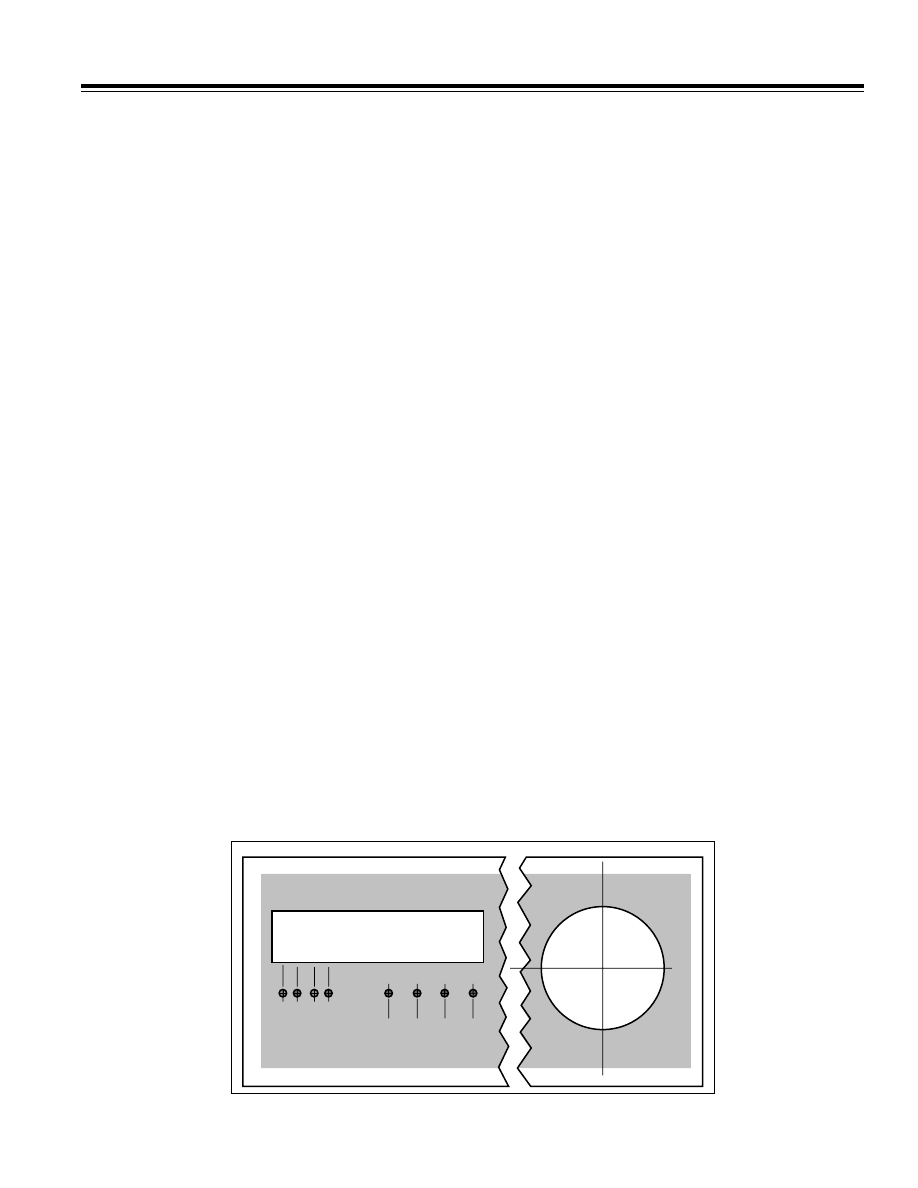
DISPLAY BOARD MOUNTING
The display board mounts immediately behind the front
panel. You will need an aperture of 3"
× 3/4" to view the
frequency readout. Having cut the aperture, you need to
back the hole with some optical filter material which
either corresponds to the color of your display (typically
red/green) or—and preferably—is circularly polarized.
The latter gives much superior performance in bright
natural light but for some reason has become expensive
in recent years.
Figure 5 is a suggested front panel template which also
shows how I have accommodated the status LEDs.
Three mm holes are drilled for these, the LEDs are
inserted in the board but not soldered. The front panel is
mounted into position, and the LEDs are adjusted in their
3"
ⴛ 0.75" DISPLAY CUT-OUT
3.25" NOMINAL HEIGHT FRONT PANEL
Rx
Tx
LSB
CW
USB
SIG
GEN
DISPLAY BOARD - 6.1"
ⴛ 2.75"
Figure 5. Drilling template for front panel. The position of the tuning knob shown assumes you are mounting the shaft
encoder on the display and DDS boards. It could be much further to the right or on the opposite side of the display.
REV. 0
–8–
AN-557
holes for equal protrusion. They are then tacked and
finally soldered to the display board when fully aligned.
If like me, you deprecate the idea of screw-heads showing
on the front panel, then you will need to glue some nuts
or threaded pillars to the back of the front panel to
mount the display board. I find nut rivets ideal for this
since they have a large surface area which makes for
strong and permanent adhesion using super glue.
DDS BOARD MOUNTING
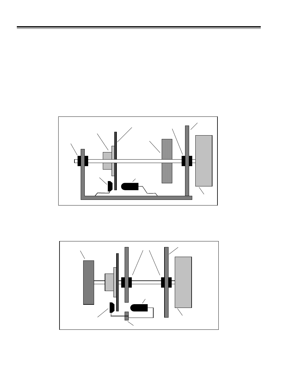
Figure 6 shows the configuration for right angle mount-
ing and Figure 7 illustrates parallel mounting.
REAR BEARING
DISC MOUNTING KNOB
ACETATE DISC
FLYWHEEL
FRONT BEARING
DISPLAY BOARD
TUNING KNOB
DDS BOARD
IR DETECTOR
IR DIODE
Figure 6. DDS board mounted at right angles to and integral with the display board. Also illustrates a suggested mounting
method (not to scale) for the shaft encoder disc, IR diode and detector. Note the long lead lengths on the latter to give simple
adjustment of diode and detector positions relative to the disc. The disc needs to be mounted near enough to the display
board to clear the x’tal oscillator enclosure to be described later. The rear bearing is mounted on a piece of PCB soldered to
the DDS board and/or the rear of the x’tal oscillator enclosure.
DDS BOARD
DISPLAY BOARD
IR DETECTOR
IR DIODE
FLYWHEEL
TUNING KNOB
BEARINGS
Figure 7. Alternative mounting method (not-to-scale) where the DDS board is mounted parallel to the display board on
spacers (not shown). A small hole is drilled in the DDS board to pass the infrared, and the rear bearings are fitted to the DDS
board. The leads for the detector pass through the board to the tracks—which are cut to avoid interference with the rear
bearing. The detail will become apparent when the DDS PCB is described later.
To ensure full access during commissioning I would
strongly recommend that you avoid the parallel mounting
configuration to start with. If this is your target configu-
ration, join the two boards with a short length of 0.1"
pitch ribbon cable. This allows access to both sides of
both boards for testing.
If you are mounting the two boards at right angles in close
proximity, then the best approach is to permanently
solder the two boards together as shown in Figure 6.
Butt the two boards to form a small “T” junction (not an
“L”), tack them lightly together, check the angle and
then run beads of solder along the full length of both

–9–
AN-557
REV. 0
sides to intimately join the ground planes. Join the
edge-connectors with a small solder bridge and test
for shorts.
A further advantage of taking this approach is that the
display board need not be secured to the front panel.
Mounting the DDS board to a horizontal base with the
display ICs touching the rear of the optical filter provides
effective location.
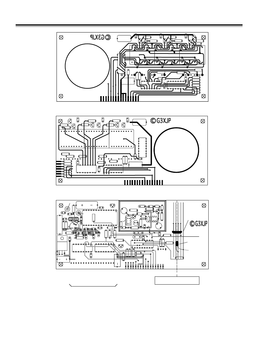
MAKING THE PCBs
In my article on the Third Method Transceiver, I
described an approach to constructing boards without
etching which proved very popular. It would be perfectly
viable to use this technique for the display board in this
project, but wholly inappropriate for the DDS board. So
what follows is a technique I have used for many years
for making one-off PCBs without the expense of UV
exposure techniques. I must emphasize that this
approach is viable only for one-offs and is hopeless if
you need greater quantities. I would also be very sur-
prised if these particular boards can be made using an
etch-resist pen, since some of the tracking is very fine.
The technique revolves around removal of material
where you want to remove copper—rather than apply-
ing resist where you want to retain copper.
The board is firstly cut to size and then drilled. For any
surface mounting areas, the board may be gently
punched but not drilled. The idea is to give yourself
guides to draw the artwork directly onto the board.
With the board clean but not polished, it is sprayed both
sides with an aerosol of car paint. Matt black is best for a
contrast color against the copper. It is important to put
on a light enough coat to just cover it, but not to get any
substantial build up of paint thickness.
Then, only after the paint is truly dry, the paint is
removed between the tracks using a scribing tool. You
use the holes, punch marks and master artwork as a
guide. You only need to remove a fine line of paint. In
fact if you stand a few feet back from the finished board,
it looks substantially like continuous copper. Note that
if, for example, you have two parallel tracks, you would
need three scribed lines to implement it.
The technique takes a little getting used to, but if you
should make a mistake, simply repaint the affected area
with a small brush and do it again—differently!
There are some important tips:
Tape the board down to a reasonable block of wood to
stop it skidding around and to prevent scratching the
paint on the reverse side. You can also use a square
against the edge of the wood if you want posh lines—
but the square needs to be transparent if you want to
avoid frustration. Use a piece of Vero board as a guide if
you need to scribe edge connectors. Scribe the board at
a good room temperature—certainly never cold. The
heat from a desk light makes it even easier and helps
prevent paint chipping.
Finally, the scribing tool itself is important. It needs to be
pointed but not incredibly so. And it also wants to retain
the point. I find the best tool is to take a masonry nail—
which is hard steel—cut the head off and grip it in a
draughtsman’s clutch-pencil. Failing that, a long masonry
nail through a cork is pretty comfortable.
Sharpen the point with a rotate and drag motion on a
piece of emery and when you have got it as sharp as you
can, blunt it ever so slightly on a piece of fine wet and
dry. Try it on a piece of scrap, holding the scribe at about
45
°, and you should get a clean fine line. Resist gouging
out the copper. You are only trying to remove paint!
Repeat the sharpening process every ten minutes or so.
You will feel when it is not cutting the paint cleanly. By
the way, for really fine work (you won’t need it here) a
sewing needle is excellent as is an old gramophone
needle.
When you have scribed both sides of the board and
checked it meticulously, etch the board in the conven-
tional manner with ferric chloride. You will find you will
get through very little FeCl because the total amount of
copper removed is very small. Observe all the usual
safety precautions. Keep the board and FeCl solution
gently on the move all the time to get an even etch and
have the courage to overetch it slightly if anything. Make
sure both sides are fully etched before removal.
Wash the board thoroughly in cold water, inspect and
etch further if necessary. Finally wash the board with hot
water and then clean off all the paint using cellulose
thinners. A small paint brush helps to get the paint out
of the holes, but being a good insulator, this is not critical.
Polish the board with fine wet and dry (used wet) or a
polishing block.
Now for the important stage. Using a continuity tester
check for isolation between each and every adjacent
track. If you find any shorts that are obvious, clear then
with a sharp blade. If they are not obvious, my practice
which I hesitate to publicize is to connect two test probes to
a car battery and then blow off the short. Be careful!
The end result is an individual piece of craftsmanship—
produced with no greater effort or time than is needed
to draw the artwork onto film in the first place. And it is
home-brew! You end up with much more ground plane
than is typical with other approaches—which can only
be to the good. And there are no critical processes in the
sense that you can see what is happening all the time
and can avoid moving on until you have got it right. I
commend it to you.

REV. 0
–10–
AN-557
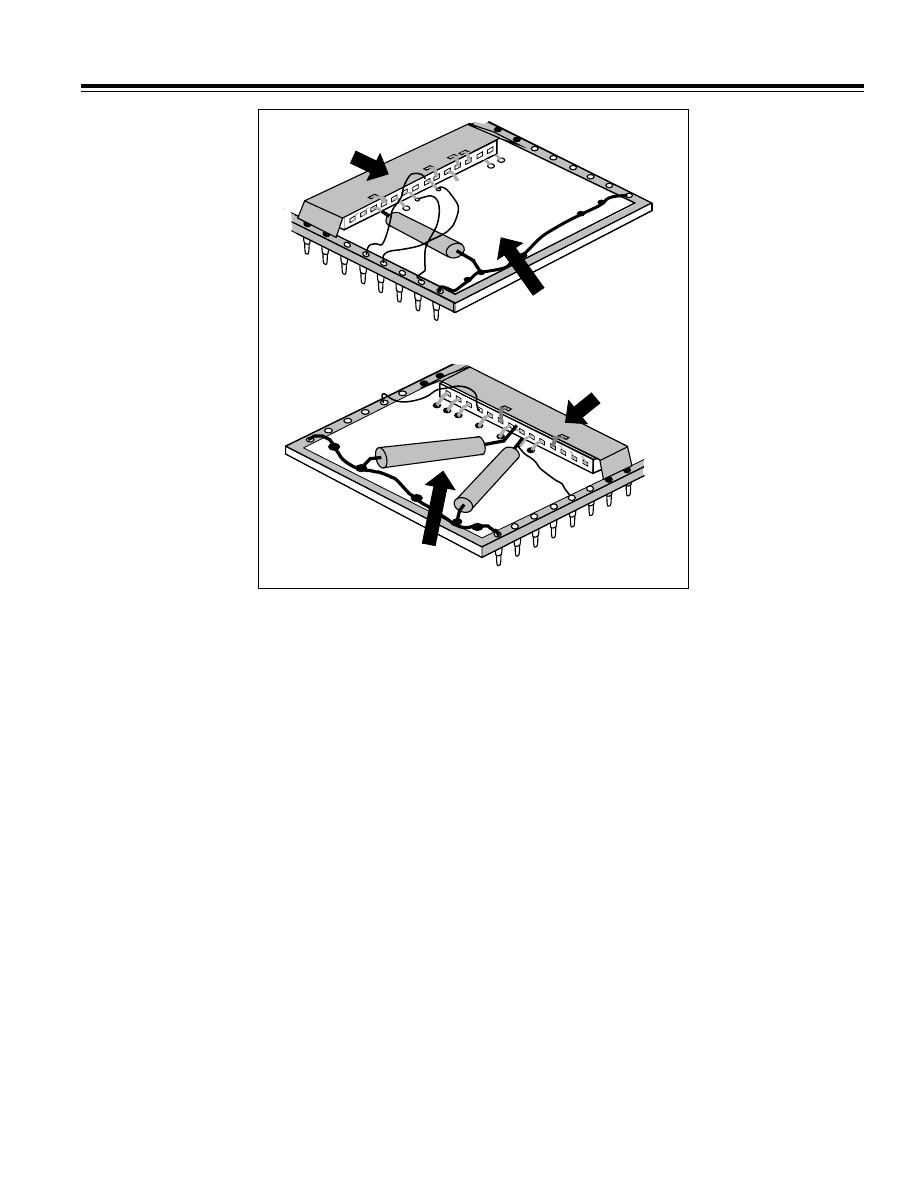
PROCEDURE FOR FITTING THE AD9850 CHIP TO A DIL
CARRIER
CAUTION: Analog Devices recommend taking proper
antistatic precautions when handling the AD9850. It
would be folly to ignore this advice with a chip of this
value.
Take a 28-pin, 0.6" wide turned-pin DIL socket and fit a
piece of PCB, copper side up into the recess between the
pins. It needs to be a snug fit. Most sockets have small
moulding pimples adjacent to Pins 1 and 14. These
should be removed with a sharp knife to allow the PCB
to lie flat.
When the PCB is the correct size for fitting, clean the
copper surface and handle it only by the edges thereafter.
Secure the PCB to the socket by soldering some tinned
copper wires between Pins 1 and 28—and Pins 14 and
15. Solder the wire to the PCB also. This secures the PCB
in place on the socket and establishes an earth connection
point on each corner.
Take the socket and secure it to something heavy
enough to allow you to work on it without it sliding
around. I use a small block of wood with some antistatic
foam stuck to it—and press the legs of the socket into
the foam to secure it.
Take the AD9850 chip, turn it over and mark Pin 1 on the
underside with a dab of paint or similar. This ensures
that even when the chip is upside down, you are still
sure which is Pin 1, thus preventing you from connect-
ing it up rotated by 180
°.
Place the chip centrally on the PCB at right angles to the
socket between Pins 7, 8, 21, and 22. Mark the position
of the chip moulding under its pins—on the PCB, using a
sharp pencil. Remove the chip.
Tin the PCB evenly in two strips about 4 mm wide under
where the chip pins will be—up to but not under the
marked moulding position. This is to facilitate soldering
the earthy pins of the chip later.
Secure the chip upside down with a trace of super glue
to the PCB. Make absolutely certain that Pin 1 on the
chip is in the same corner as Pin 1 on the socket.
Check it again!
Please follow the rest of this process without creativity.
The result is illustrated in Figure 8. I have hand mounted
about 10 chips to optimize the process and carefully
observed others deviate (on practice chips!) and get it
wrong. The source of error is always operating on the
wrong pin. Although this may seem surprising, when
you have tried it yourself you will understand why.
From now on, work only in full natural daylight. The idea
is to work down one side of the chip, never taking your
eyes off the job. Should you do so and have to start
recounting the pins, this has proved to be the single
largest source of errors.
You only get one chance to get it right so you must get
some help to dictate the following sequence to you—so
you can stay focused on the job.
The best tool for bending pins is a Stanley knife blade.
Push on the end of the pin with the point of the blade in
the required direction. Not far at this stage; just enough
to be sure of the intended direction later.
In this sequence, “down” means bend the pin towards
the PCB. “Up” means bend it away from the board, ap-
proximately vertically upwards. “Leave” means do
nothing.
1
down
2
down
3
up
4
up
5
down
6
up
7
leave
8
leave
9
leave
10
down
11
up
12
leave
13
leave
14
leave
Now focus on infinity and walk around for several minutes
before addressing the other side.
15
leave
16
leave
17
leave
18
up
19
down
20
leave
21
leave
22
down
23
up
24
down
25
leave
26
down
27
down
28
down
That completes the tricky bit!
Bend down Pins 1 and 2 to within about 1 mm of the
tinned surface and then solder them to the PCB.
To solder the pins to the copper, the best technique is to
place the iron on the board about 2 mm back from the
pin(s) and hold it there for a couple of seconds to heat
the mass of the PCB. Then form a small blob of solder
on the PCB and push it towards the pins. On contact,
remove the iron almost immediately.
–11–
AN-557
REV. 0
Repeat this process for Pins 19, 26–28, 10, 22, 5, and
24 in that order. Make very sure you are operating on
the correct legs. You can bend them up and down
perhaps once before risking amputation but it is not
worth the risk.
Obtain a small strip of copper foil. Copper or brass shim
stock would suffice. In the worst case, a suitable strip
can be removed from a piece of scrap PCB with a sharp
knife or stripped from some foil braided coax.
It needs to be long enough to solder to Pins 7 and 8 of
the socket, pass over the chip and down the other side to
solder to Pins 21 and 22. The width needs to be the same
as (or if anything, a whisker more than) the chip moulding
width. It can be trimmed to size and trial fitted for
width with a pair of scissors. Excess length can be
removed later.
Fix the foil to the chip moulding using a trace of super
glue. When set, bend the ends down, trim to length and
solder to the +5 V pins on the DIL socket (7 and 8, 21
and 22), making sure that it does not touch the PCB
ground plane.
Bend up completely all the +5 V pins on the chip, namely
3, 4, 6, 11, 18, 23 and then quickly solder each one to
the foil.
15
REFOUT
100R
200R
28
7
8
9
10
11
12
13
14
15
16
17
18
19
20
21
22
15
18
23
D7 = RB4
PCB
GROUND PLANE
COPPER FOIL
POWER PLANE
5V
3k9
1
COPPER FOIL
POWER PLANE
5V
PCB
GROUND PLANE
2
3
4
5
6
7
8
1
3
4
6
11
14
21
22
23
24
25
26
27
28
FQ_UD = RB5
FQ_CLK = RB6
CLKIN
Figure 8. DDS assembly. The DDS chip is mounted upside down (dead-bug) on the PCB ground plane. A strip of copper foil
provides a low impedance power plane. Not shown is a 1n decoupling capacitor connected between the ground and power
planes adjacent to Pin 1 on the chip.
There now remains only to attach seven signal pins and
to ease the process, some pins are bent down a little to
near horizontal and some up a few degrees. This gives
more clearance to get the soldering iron in. Bend Pins 8,
21, 25 up a little and Pins 7, 9, 12, 20 down a little.
Trim the three resistors to size and solder down their
earthy ends with the pin end just touching the end of the
target pin, bending the resistors leads as necessary to
get a touch on the end of the pins. Quickly solder the
resistors to the pins.
Take some enamelled copper wire, very thin but not
critically so. Vero wire is ideal. Make off the end of the
wire on the DIL socket end first and then trim the wire to
length. With the end of the wire and the end of the pin
both pretinned, and a clean tinned iron, solder the wire
to the pin (and in one case, to the resistor lead). The best
order is 7, 9, 25, 20, and 8.
Pins 13–17 are not connected.

REV. 0
–12–
AN-557
PART 3 OF 5
In this issue the circuit diagram and PCB layout for the
display board is described together with some construc-
tion notes and the complete project components list.
DISPLAY BOARD DESCRIPTION
Referring to Figure 11, the display element itself comprises
three double-digit seven-segment common anode
displays. They were chosen because they are large and
make for comfortable viewing. Their segments are all
wired in parallel.
1
4
7
2
5
8
3
6
9
0
USB
Rate
Cal
CW
Scan
Mem
A/B
A=B
Split
#
LSB
Freq
Save
Figure 9. Keypad Overlay for Reproduction, 47 mm
Wide by 57.5 mm High
It is traditional to drive 16 character backlit LCD displays
in this sort of application. The cost would be comparable
(for a one-off), power consumption noticeably less and
the software complexity about the same, albeit totally
different in nature. I preferred the LED approach since
I find the LCD character size just a little small for com-
fortable viewing.
The display digits are multiplexed; that is, only one digit
is lit at any one time, and all are lit in turn (rapidly and
frequently) to provide flicker-free viewing. The software
controls the multiplexing process and devotes as much
time to repainting the display as circumstances permit.
In operation, IC12 decodes RA0, 1, 2 to determine which
one digit is being addressed—driving one of the PNP
switches Tr5–Tr10 to handle the digit current. At the
same time, IC11 decodes a BCD input on RB0, 1, 2, 3 to
determine which segments to light; and in addition RA3
is pulled low for a decimal point. By rushing round each
digit in turn and by executing the entire sequence
often enough, the human eye sees a continuous six-
digit display.
Do not be tempted to substitute a different BCD to
seven-segment decoder chip, since the software relies
on the behavior of the ‘LS47 for BCD values greater than
nine to achieve leading zero suppression.
Data is clocked into the latch IC13 as an 8-bit serial
word —and the outputs are updated by a latch pulse on
RB5. These bits drive low current (2 mA) LEDs (D4-D11)
directly via current limiting resistors R41–R48. D4 and
D5 are green LEDs, the others red. This gives a strong
visual clue when you are operating “split.”
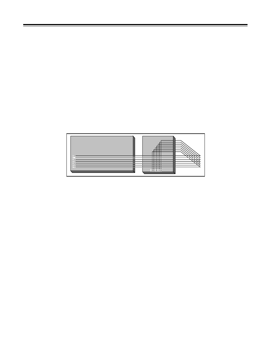
The seven lines to the keypad are routed through the
display board for convenience. They could equally be
taken directly from the DDS board provided some
means is found to mount the series resistors R49–R55.
The resistors are there to prevent potential short-
circuiting of the PIC I/O lines in the event that two or
more keys are pressed simultaneously.
KEYPAD
The keypad is a low cost four-row by three-column
switch matrix designed for push-button phones. The
software polls the keypad periodically looking for key
presses. It does this by driving each row low in turn. For
each row, it then tests each column looking for a low
and if one is found, the column/row intersection defines
which key is pressed. The key press is de-bounced in
software since the contacts rapidly make and break for
up to 5 ms—and without this facility, the average key
press would otherwise be interpreted as about 20
successive identical key presses.
The keypad needs an overlay to give a better feel of the
alternative meaning of the keys in this application.
Figure 9 may be copied at size and glued over the keys,
the digits having been first cut out with a sharp knife.
The keypad is connected to the display board via some
seven-way ribbon cable. You need a cable routing which
brings the top lead from the display board to the most
right-hand connector on the keypad.
–13–
AN-557
REV. 0
DISPLAY BOARD
KEYPAD
Figure 10. Display board to keypad ribbon cable routing viewed from the front. Note that of the eight connectors on the
keypad, the extreme left one is not connected.
Figure 10 shows the best way to achieve this. The cable
is routed across the front of the display board beneath
the frequency display and LEDs. It then passes behind
the keypad and somewhat beyond it. The cable is then
folded back on itself—i.e., through 180
°—and then
folded downwards through 90
°. It is then made off onto
the seven right-most pads on the keypad. This process
produces a neat cable run with the correct connections.
DISPLAY BOARD CONSTRUCTION NOTES
The PCB layout is shown in Figure 12. The rear tracking
is somewhat complex around the display IC sockets. A
perfectly acceptable but less purist approach would be
to bring these pins and those of IC11 out onto small
pads and then hand wire all the segments to the seven-
segment decoder using Vero wire.
Other common anode devices, including single-digit ICs
and those with pins on the vertical edges could easily be
substituted with simple changes to the PCB—or again,
by using Vero wire.
The status LEDs may be tacked onto the board but with-
out shortening their leads for commissioning purposes.
When inserting ICs or IC sockets onto the board with this
form of PCB construction, insert them only far enough to
give a useful tail on the back of the board. Specifically,
avoid bridging tracks or earthling pins on the component
side of the board via the shoulders on the pins.
REV. 0
–14–
AN-557
IC12
74LS138
BCD TO
7-SEG
DECODER/
DRIVER
G1
G2A
3-TO-8
DECODER
G2B
A
B
C
14
1
2
3
4
5
6
13
12
10
9
R35
2.2k
⍀
TR5
BC327
TR6
BC327
TR7
BC327
TR8
BC327
TR9
BC327
TR10
BC327
7, 15 NOT
CONNECTED
1
2
3
RA0
RA1
RA2
IC11
74LS47
A
B
D
C
4, 5 NOT
CONNECTED
V
SS
a
R36
2.2k
⍀
R37
2.2k
⍀
b
c
d
e
f
g
V
DD
LT
16
3
13
12
11
10
9
15
14
a2
b2
c2
d2
e2
f2
g2
ANODE1
14
13
11
10
8
6
5
12
9
ANODE2
IC8
DIGITS 1&2
dp1
a1
b1
c1
d1
e1
f1
g1
dp2
7
16
15
3
2
1
18
17
a2
b2
c2
d2
e2
f2
g2
ANODE1
14
13
11
10
8
6
5
12
9
ANODE2
IC9
DIGITS 3&4
dp1
a1
b1
c1
d1
e1
f1
g1
dp2
7
16
15
3
2
1
18
17
a2
b2
c2
d2
e2
f2
g2
ANODE1
14
13
11
10
8
6
5
12
9
ANODE2
IC10
DIGITS 5&6
dp1
a1
b1
c1
d1
e1
f1
g1
dp2
7
16
15
3
2
1
18
17
R38
2.2k
⍀
R39
2.2k
⍀
R40
2.2k
⍀
8
8
4
4
4
7
1
2
RB0
RB1
6
D3
1N4148
5V
SERIAL IN
PARALLEL OUT
SHIFT REGISTER
AND LATCH
IC13
4094
DATA
LATCH
9, 10 NOT
CONNECTED
V
SS
Q2
Q1
Q7
Q5
Q6
Q8
Q3
V
DD
OE
16
5
4
12
14
13
11
6
8
1
2
5V
Q4
7
RB5
RB2
RB3
RA3
3
CLOCK
R41
3.3k
⍀
R42
3.3k
⍀
15
R
X
= VFO "A"
R43
3.3k
⍀
R44
3.3k
⍀
R45
3.3k
⍀
R46
3.3k
⍀
R47
3.3k
⍀
R48
3.3k
⍀
T
X
= VFO "A"
R
X
= VFO "B"
T
X
= VFO "B"
LSB
CW
USB
SIG GEN MODE
R49
470
⍀
RA2
RB0
RB1
RB2
RA1
RA0
RB3
R51
470
⍀
R52
470
⍀
R53
470
⍀
R54
470
⍀
R55
470
⍀
R50
470
⍀
D4
D5
D6
D7
D8
D9
D10
D11
C39
10nF
C38
10nF
C37
10nF
C36
10nF
C35
10nF
C34
10nF
RB4
5V (FROM DDS BOARD)
C40
100
F
C41
100
F
FROM
DDS
BOARD
TO 4x3
KEYPAD
VIA 7-WAY
RIBBON
CABLE
V
DD
6
4
5
11
Figure 11. Display board circuit diagram. Note that the segments of all the display ICS (8, 9, 10) are wired in parallel except
for some decimal points which are never used and which are not connected. The eight 3 mm status LEDs, D4–D11 are soldered
on the display board, but physically mounted in holes in the front panel.

–15–
AN-557
REV. 0
COMPONENTS LIST
Resistors . . . . . . . . . . . . . 1/8–1/4 W, 5%–10% except R33
R1, R9, R17, R27–31 . . . . . . . . . . . . . . . . . . . . . . . . . 100R
R2 . . . . . . . . . . . . . . . . . . . . . . . . . . . . . . . . . . . . . . . . 330R
R3, R4 . . . . . . . . . . . . . . . . . . . . . . . . . . . . . . . . . . . . . . 10k
R5, R14, R20, R21, R23 . . . . . . . . . . . . . . . . . . . . . . . . . 1k
R6 . . . . . . . . . . . . . . . . . . . . . . . . . . . . . . . . . . . . . . . . 220R
R7, R8, R22 . . . . . . . . . . . . . . . . . . . . . . . . . . . . . . . . . . 4 k 7
R10 . . . . . . . . . . . . . . . . . . . . . . . . . . . . . . . . . . . . . . . 200R
R11 . . . . . . . . . . . . . . . . . . . . . . . . . . . . . . . . . . . . . . . 180R
R12, R15 . . . . . . . . . . . . . . . . . . . . . . . . . . . . . . . . . . . . 56R
R13, R49–55 . . . . . . . . . . . . . . . . . . . . . . . . . . . . . . . . 470R
R16 . . . . . . . . . . . . . . . . . . . . . . . . . . . . . . . . . . . . . . . 5 R 6
R18 . . . . . . . . . . . . . . . . . . . . . . . . . . . . . . . . . . . . . . . . 3 k 9
R19 . . . . . . . . . . . . . . . . . . . . . . . . . . . . . . . . . . . . . . . 560R
R24–26 . . . . . . . . . . . . . . . . . . . . . . . . . . . . . . . . . . . . 270k
R32 . . . . . . . . . . . . . . . . . . . . . . . . . . . . . . . . . . . . . . . . 47k
R33 . . . . . . . . . . . . . . . . . . . . . . . . . . . . . . . . . . . . 10R, 2W
R35–40 . . . . . . . . . . . . . . . . . . . . . . . . . . . . . . . . . . . . . 2 k 2
R41–48 . . . . . . . . . . . . . . . . . . . . . . . . . . . . . . . . . . . . . 3k3
Capacitors
TC1, TC2 . . . . . . . . . . . 2–22p min film dielectric trimmer
C1 . . . . . . . . . . . . . . . . . . . . . . . . . . . . . . . 1n feedthrough
C2, C4, C5, C11–14, C17, C18 . . . . . . . . . 1n disc ceramic
C3 . . . . . . . . . . . . . . . . . . . . 10
µ, 16 V radial electrolytic
C6, C24, C28 . . . . . . . . . . . . . . . . . . . . . 22p ceramic plate
C7 . . . . . . . . . . . . . . . . . . . . . . . . . . . . . 68p ceramic plate
C8, C9, C40, C41 . . . . . . . . . 100
µ, 10v axial electrolytic
C10, C16, C19-23, C34–39 . . . . . . . . . . . 10n disc ceramic
C15 . . . . . . . . . . . . . . . . . . . 470
µ, 16 V axial electrolytic
C25 . . . . . . . . . . . . . . . . . . . . . . . . . . . . 3p3 ceramic plate
C26 . . . . . . . . . . . . . . . . . . . . . . . . . . . . 33p ceramic plate
C27 . . . . . . . . . . . . . . . . . . . . . . . . . . . . 8p2 ceramic plate
C29, C30 . . . . . . . . . . . . . . . . . . . . . . . . 15p ceramic plate
C31, C32 . . . . . . . . . . . . . . . . . . . . . . . . 47p ceramic plate
C33 . . . . . . . . . . . . . . . . . . . . . . . . . . . 100p ceramic plate
Semiconductors
D1 . . . . . . . . . . . . . . . . . . . . . . . . . . . . . . . LD271 IR diode
D2, D3 . . . . . . . . . . . . . . . . . . . . . . . . . . . . . . . . . . 1N4148
D4, D5 . . . . . . . . . . . . . . . 3 mm low current LED (green)
D6–D11 . . . . . . . . . . . . . . . . 3 mm low current LED (red)
IC1 . . . . . . . . . . . . . . . . . . . . . . . . . . . . . . . . . . . . . . . 78L08
IC2 . . . . . . . . . . . . . . . . . . . . . . . . . . . . . . . . . . . . . . . . 7805
IC3 . . . . . . . . . . . . . . . . . . . . . . . . . 16C84-04/P (in socket)
IC4 . . . . . . . . . . . . . . . . . . . . . . . . . . . . . . . . . . AD9850BRS
IC5 . . . . . . . . . . . . . . . . . . . . . . . . . . . . . . . . . . . . HLC2705
IC6, IC7, IC13 . . . . . . . . . . . . . . . . . . . . 4094 (no sockets)
IC8–IC10 . . . . . . . . . . 2-digit common anode 7-seg LED,
Maplin FA01B (green) or BY66W (red)
IC11 . . . . . . . . . . . . . . . . . . . . . . 74LS47 (socket optional)
IC12 . . . . . . . . . . . . . . . . . . . . . . . . . . 74LS138 (no socket)
Tr1 . . . . . . . . . . . . . . . . . . . . . . . . . . . . . . . . . . . . 2N2222A
Tr2 . . . . . . . . . . . . . . . . . . . . . . . . . . . . . . . . . . . . . . . J310
Tr3 . . . . . . . . . . . . . . . . . . . 2N3866 with small heat sink
Tr4 . . . . . . . . . . . . . . . . . . . . . . . . . . . . . . . . . . . . . BC108
Tr5-10 . . . . . . . . . . . . . . . . . . . . . . . . . . . . . . . . . . . BC327
Inductors
L1 . . . . . . . . . . . . . . . . . . . . . . 5 turns 22 swg on 1/4" dia,
1/2" long, tap 1 turn from earthy end
L2 . . . . . . . . . . . . . . . . . . . . . . 5 turns 22swg on 1/4" dia,
1/2" long, centretap
L3 . . . . . . . . . . . . . . . . . . . . . . . . . . . . . . 1
µH axial choke
L4 . . . . . . . . . . . . . . . . . . . . . . . . . . . . 0.68
µH axial choke
T1 . . . . . . . . . . . . . . . . 8 bifilar turns 32 swg on FT37-43
Miscellaneous
2-sided PCB . . . . . . . . . . . . . . . for dimensions see text
Keypad 4x3 . . . . . . . . . . . . . . . . . . . . . . . . Maplin JM09K
7-way 0.1" pitch ribbon cable for above
1-off . . . . . . . . . . . . . 32-pin DIL turned pin socket (0.6")
1-off . . . . . . . . . . . . . 28-pin DIL turned pin socket (0.6")
Mount display ICs on above and cut off unused pins
Display optical filter, 3.5"x1" approx.
1-off . . . . . . . . . . . . . . . . . . 28-pin DIL turned pin socket
(0.6") for DDS assy
1-off . . . . . . . . . . . . . . . . . . 28-pin DIL turned pin socket
(0.6") to mount DDS assy on mother board
1-off . . . . . . . . . . . . . . . . . . 18-pin DIL turned pin socket
(0.3") for 16C84
1-off . . . . . . . . . . . . . . . . . . 14- pin DIL turned pin socket
(0.3") for 74LS47 (optional)
Shaft encoder disc . . . . . . . . . . . . . . . . . . . . . . . see text
Knob to mount encoder disc, approx 1" skirt dia, drill
right Tuning knob, flywheel, shaft and
bushes/bearings . . . . . . . . . . . . . . . . . . . Your choice!
18-way ribbon cable to Tx/Rx . . . . . . . . . . . . (optional)
16-way inter-board ribbon cable . . . . . . . . . . (optional)
12 V dc input connector . . . . . . . . . . . . . . . . . (optional)
RF output connector . . . . . . . . . . . . . . . . . . . . (optional)
18-way host connector . . . . . . . . . . . . . . . . . . (optional)
X1 . . . . . . . . . . . . . . . . . . . . . . approx 110 MHz (see text)
X2 . . . . . . . . . . . . . . . . . . . . . . . . . . . . . . . . . . . . . . . 4 MHz
SUPPLIERS
THE MAJORITY of the above components were purchased
from JAB Electronic Components, PO Box 5774, Great
Barr, Birmingham, B44 8PJ. Tel 0121 6827045. They of-
fer an excellent service.
The significant exceptions are the keypad, IC8–IC10, D1,
D4, D5, D6–D11, Tr1 which are available from Maplins.
The PIC 16C84 (IC3) can also be obtained from Maplin at
a 1—off price of £8.90—if you want to write your own
software. I will be happy to supply the PIC ready pro-
grammed with the features described in this article, an
acetate disc for the shaft encoder and a paper overlay
for the keypad for £15, on receipt of an SAE.
For bushes and bearings, much can be recovered from
scrap potentiometers or variable capacitors. Failing that,
model shops are a good source.
The AD9850BRS DDS chip can be purchased through
any Analog Devices distributor who will sell small
quantities. There may be a long lead time. The price will
depend on delivery and payment methods. I used Kudos
Thame Ltd., 55 Suttons Business Park, Reading, Berks
RG6 1AZ. Tel 0118 935 1010.
REV. 0
–16–
AN-557
Figure 12. Display board PCB drawn for production as described in the text. The ground plane is not shown since all of the
board (both sides) is ground plane copper except where removed to let in the tracking. Holes on the front and rear track views
shown as an “x” are not soldered on that side of the board. They should be lightly countersunk. Holes shown as an “o“ are
soldered to either the track or the ground plane. All holes are 0.7 mm dia. The front panel LEDs (D4–D11) are not shown. They
solder to the pad and ground plane pairs in a horizontal line about half way up the rear view. Nine short wire links are shown
as pecked lines on the rear view.
REAR VIEW – (NONCOMPONENT SIDE) SHOWING REAR TRACK AND SOLDERING POINTS
FRONT VIEW – (COMPONENT SIDE) SHOWING FRONT TRACK AND SOLDERING POINTS
18MHz
C17
RA0
RA1
RA2
RA4
RA3
5V
C20
12V
R17
C15
IC1
RFOUT
R33
R16
R15
TR3
T1
C22
IC2
C16
C8
6.1" x 2.75"
C19
C28
C26
C24
R11
R12
C23
C27
C25
C12
R7
R28
DDS ASSY
COMPRISING
IC4, R9, R10,
R18, C14
C9
R32
R26
R25
R24
D2
R23
IC3
PROGRAMMER
INTERFACE
ONLY
MCLR
RB7
0V
RB6
DIRECTION
PULSE
R19
DIODE
ANODE
D1
IR DETECTOR
IC5
R20
R21
C18
C13
X2
R31
R30
SLOTTED DISC
51MM DIA
C30
C29
TR4
R22
R8
R27
R29
C10
R13
C21
L4
L3
C7
TC2
R6
X1
C33
C31
R4
R3
TR1
L1
L2
R2
TC1
R1
C3
R5
C32
C6
C5
C4
C2
15MHz
14MHz
29MHz
28MHz
24MHz
21MHz
10MHz
0V
USE CW IF
USE USB IF
USE LSB IF
7MHz
3.5MHz
1.8MHz
BROADBAND
[SPARE]
T/R (PTT LINE)
RB1
RB2
RB3
RB0
RB5
0V
SHAFT CENTER LINE
TUNING KNOB
(NOMINALLY 1.75" DIA)
LOGIC INTERFACE TO Tx/Rx
NB ALL TRACKS MARKED 0V
ARE CONNECTED TO
THE GROUND PLANE
TOP VIEW – SHOWING COMPONENT LOCATION AND DRILLING TEMPLATE
5V
0V
IC6
IC7
C11
C1

–17–
AN-557
REV. 0
PART 4 OF 5
In this issue the circuit diagram and PCB layout is
provided for the DDS board together with some con-
struction notes and details for building a shaft encoder.
DDS BOARD DESCRIPTION
Referring to Figure 13, the functional blocks comprise an
x’tal oscillator (the reference clock) feeding the DDS
assembly, followed by a low-pass filter and buffer.
There are two output latches and not least, the PIC
which controls operations.
On the input side, the PIC is monitoring the shaft encoder,
the PTT line and the keypad. Tr1 is a conventional x’tal
oscillator followed by Tr2, a common gate buffer. The
crystal may be any value in the range 100 MHz–125 MHz,
the higher the better. The exact achieved frequency is
trimmed into the software using the calibration process
described next month.
The entire oscillator is surrounded by a PCB enclosure
formed by the board, four sides and a top. The latter has
braid hinges for access—and two holes drilled to allow
adjustment of TC1 and TC2. R7 and R8 bias the AD9850
reference clock input to half rail.
IC4, the AD9850, is operated in serial control mode. That
is, a pulse stream of 32-data bits and eight control bits is
clocked serially in on the D7 line by 40 corresponding
clock pulses on W_CLK. That sequence is then actioned
by pulsing FQ_UD high.
The resulting synthesized sine wave appears on the
complimentary current outputs IOUT and IOUTB, termi-
nated by R9 and R10. R18 sets the on-chip DAC full-scale
output current in accordance with the manufacturer’s
recommendations.
C24–28 and L3, L4 form a 42 MHz, 200
Ω elliptic low-pass
filter taken from the AD9850 data sheet. R11, R12 form
an “L” pad to terminate the filter and to match into the
base of the driver Tr3. This in turn delivers +7 dBm into
50
Ω. It is important that PIC “N” MIX feeds a nonreac-
tive load of about 50
Ω to ensure effective termination of
the LPF. The injection port of, say, an SBL-1 mixer is
ideal. Being double balanced it also reduces the AM
noise floor.
Data is clocked into the latches IC6 and IC7 serially by a
sequence of eight clock pulses followed by a latch pulse.
Pulses for other purposes appear on the data and clock
lines but are effectively ignored since there is no follow-
ing latch pulse.
These two latches as well as IC13 on the display board
and the AD9850 are updated simultaneously by pulsing
RB5 high which is reserved exclusively for this purpose.
The latch outputs are +5 V when true, so you may interface
these with transistor switches etc. to drive the band
switches in your Tx/Rx, switch antennas etc.
The “broad band” output goes true if the displayed
frequency is not one of the explicitly specified ones.
(To be precise, the 10 MHz and 1 MHz digits are compared).
I use this to switch in two relays which short-circuit my
Rx front-end and remove all selectivity. This allows me
to listen on any HF frequency. Obviously Rx performance
is seriously compromised under these circumstances,
but for the ability to listen to broadcast stations, frequency
standards etc., the price is well worth paying. Equally, if
your Rx does not have a front-end for an explicit band
you could diode-OR the bit for that band with the broad
band bit.
IC3, the PIC has been covered previously. Its hardware
configuration is entirely conventional. The three lines
shown as “Programmer interface” together with R30
and R31 may be omitted if you never have any intention
of programming the PIC in situ.
D1 is a cheap IR emitter designed for remote control
applications. IC6, the IR detector is designed for computer
mouse position encoding. It has the merit of producing
decoded outputs which are very easy (and fast) to
handle in software. The “pulses” output goes briefly low
for every dark/light transition. This is used to interrupt
the PIC to handle the consequences. The “direction”
output is a steady level which reflects the last direction
of rotation. The software can, therefore, test this line at
any time pretty well at leisure to determine tuning direc-
tion. This is far cheaper on program size than decoding
the gray code outputs produced by many commercial
shaft encoders.
Tr4 isolates the host transceiver PTT line. The logic on
the PTT line can be of either polarity since the software
assumes the initial level at switch-on corresponds to
receive. This allows for your not connecting a PTT line if
you are running an Rx only. But if running a Tx/Rx this
line must be connected since the software needs to
know the T/R state in order to allow split operation; and
for safety reasons, to cancel any scanning operations
when appropriate.

REV. 0
–18–
AN-557
Construction Notes
There is a preferred order for building and commissioning
the DDS board to ensure access and progressive testing.
The PCB layout is shown in Figure 14.
Build the 110 MHz crystal oscillator first. That is, all the
components within the screening enclosure (but not the
enclosure itself) and omitting for now C1 and C7.
The oscillator components are all surface mounted on
islands on the top copper plane. The leads must be cut
as short as practicable, consistent with being able to get
the iron in. Mount the two coils L1 and L2 last. Fit the tap
to L1.
Fit also C15, IC1 and C18 and insert a temporary jumper
from the 8 V top track to the junction of R1 and C2 to
provide power to the oscillator.
Loosely couple a GDO (as a passive detector) to L2 and
set the GDO to your crystal frequency. Adjust TC1 for
oscillation and peak TC2 for maximum output at the
specified frequency. Repeat several times and check
that the oscillator fires up from cold.
Next fit the interplane wire links (i.e., some old component
leads) which are either under the PIC socket or between
it and the edge connector.
Fit IC2 and solder its tab to the board. Fit C8-C10, R23
and R33. This completes the +5 V rail distribution. Check
for shorts, apply 12 V and verify +5 V is available on the
top track busbar under the shaft encoder detector—second
track from the left. If it is getting this far, all the several
crosses from top to bottom track are verified.
Fit, in order, C29, C30, Tr4, R22, R32, R26, R25, D2.
Check again the links under the PIC socket (IC3), your
last chance, and fit the socket. Now fit R24, C13 and X2.
Now surface mount all the components in the low-pass
filter and buffer amplifier. Fit the transistor Tr3 last and
its heat sink last of all.
Temporarily fit C7, one end to the top track shown, the
other forming the centre tap on L2.
Solder IC5 and D1 to the board without shortening their
leads and adjust them so that they are about 1 cm apart.
Fit the socket ready for the DDS Assembly but do not
insert the assembly itself at this stage. Mount all other
components except C1. Insert IC3 in its socket.
Build the display board and link it to the DDS board.
Check all the interboard leads for any shorts to earth and
for any shorts to any and every other such lead.
Apply 12 V and your display should initialize to 80 m and
the Rx = “A,”’ Tx = “A” and LSB LEDs should light. This
all verifies that the PIC is working—as well as the Display
board. At this stage there is, of course, no actual RF output.
A screwdriver passed between IC5 and D1 from left to
right should produce a decrease in indicated frequency—
and vice versa right to left.
Wire up the keypad and check that all keys work—as
well as the status LEDs.
Verify +5 V on the DDS Assembly socket and check for
any shorts or bridges on all connected pins.
Finally, and only if everything else is working, insert the
DDS Assembly, monitor for RF output from the board
and apply power. Look for RF around 12 MHz–13 MHz. If
there is no output, try peaking TC1 and TC2.
All being well, Key “83” to give signal generator mode.
The RF output should change to 80 m and the status
indicator LEDs should correspond.
Fit the screened compartment around the 110 MHz
oscillator, drilling holes for C1 and for one of C7s leads to
pass through. This compartment must be made from
two-sided fiberglass board, since both its screening and
thermal conductivity properties are needed. Fit a top,
drilling holes for adjustment of TC1 and TC2. Secure the
top using some internal braid hinges.
Repeak TC1 and TC2 for clean stable output at some
known frequency—and specifically ensure the output is
not at a multiple or submultiple of that frequency.
Fit the shaft encoder. Adjust its disc, IC5 and D1 so that
the disc runs just not touching IC5. The position of D1 is
less critical (actually, none of it is very critical). It needs
to be a about 1 cm away from the disc. Note that in
bright incident light, the shaft encoder will not work
reliably and may produce no or apparently random
pulses. It is easy—but less than useful— to end up with a
device which produces an output frequency proportional
to the number of passing clouds!
Fit IC6 and IC7 last of all since their operation is indepen-
dent of the rest of the board.
You do not need the PTT line connected for testing
purposes, but should do so before starting serious
operational use.
If there is evidence of multiplex noise in your receiver, fit
a 1000
µF 15 V electrolytic from the junction of R33 and
IC2 to earth. Multiplex noise is characterized by disap-
pearing completely in sleep mode [73].

–19–
AN-557
REV. 0
If there are occasional musical tones, these may be
reduced by fitting three further decoupling capacitors
(as well as C14), one in each corner of the DDS assembly
from the 5 V power plane to the ground plane. Use two
10 n and a further 1 n with the shortest possible leads.
SHAFT ENCODER
THE shaft encoder assembly comprises a tuning knob, a
length of shafting, some bearings, a flywheel and an
encoder disc. You will also need some means of taking
out any end-float on the shaft. I was fortunate in that
Jack, G3XKF turned up some beautiful brass fittings for
me. Don’t skimp on the mechanics here as the “feel” of
the tuning knob is important to pleasurable operation.
At the very least, the assembly must spin freely with
no binding.
I borrowed a flywheel from an old cassette recorder and
drilled it out to take the shaft. Because of the software
flywheel, you don’t need much physical mass here, but
some inertia is needed to smooth the turning rate. A
heavy tuning knob may be sufficient. Mine is loaded
with lead caps off wine bottles, thereby doubling the
pleasure. While on the subject of tuning knobs, one with
a finger hole or a turning (tram) handle is best.
The software has been tuned for an encoder disc with
180 spokes. Since the detector emits a pulse for every
dark/light transition, this gives a natural tuning rate of
360
× 10 Hz = 3.6 kHz per rev, a rate which is speeded up
or slowed down by the software as appropriate.
Figure 15 shows the Disc I used which may be reproduced
at size onto acetate film (by your local copy shop). Ensure
the “spokes” reproduce black with as much contrast to
the “slots” as possible. Glue it carefully onto an old
knob with the toner side away from the detector to avoid
scratching. Drill the knob right through first and ensure
the disc is properly centered by spinning it (slowly!) on a
shaft before the glue has fully set.
Long parallel tracks are provided on the DDS board to
give flexibility in mounting position. The actual configura-
tion will depend on whether the DDS board is mounted
parallel to or at right angles to the display board.
Next Month
This article concludes with the calibration process and
details of user operation.
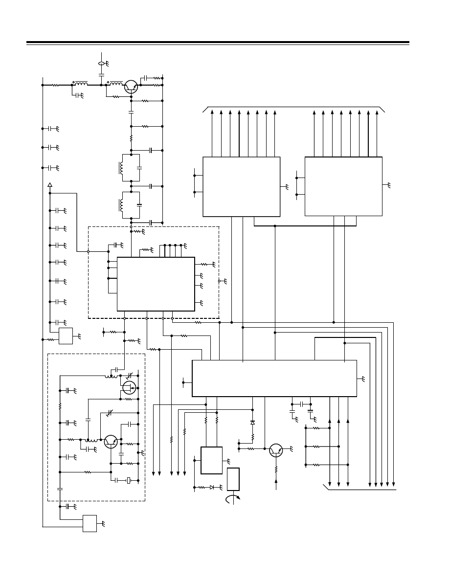
REV. 0
–20–
AN-557
IC6
4094
CLOCK
LATCH
DATA
V
SS
V
DD
16
15
4
14
13
12
11
5
6
8
1
2
3
5V
7
SERIAL IN
PARALLEL
MUST
SHIFT
REGISTER
& LATCH
IC6
4094
9, 10 NOT
CONNECTED
V
SS
Q1
Q5
Q6
Q7
Q8
Q2
Q3
V
DD
OE
16
15
4
14
13
12
11
5
6
8
1
2
3
5V
Q4
7
IC3
16C84
PIC
V
SS
V
DD
14
5
4
3
5V
10
12
11
IC4
AD9850
PIC
5, 24
22
12
10, 19
RESET
27
1
26
28
2
23, 6
11, 18
3
4
C14
1nF
25
7
8
IOUT
C24
22p
L3
1.0
H
L4
0.68
H
R11
180
⍀
R12
56
⍀
R16
56
⍀
R17
100
⍀
20
21
RFOUT
R14
1k
⍀
R15
56
⍀
R13
470
⍀
C21
10nF
C28
22p
C26
33p
C20
10nF
TR3
2N3866
T1
R10
200
⍀
R9
100
⍀
C25
3.3p
D7
W_CLK
FQ_UD
13, 14, 15, 16, 17
NOT CONNECTED
V
DD
R7
4.7k
⍀
13
2
OSC2
16
15
C30
15p
17
18
1
D2
IN4148
R23
1k
⍀
TR4
BC108
5V
R32
4.7k
⍀
IC5
HLC2705
IR
DETECTOR
3
SLOTTED
DISK
2
D1
LD271
R19
560
⍀
R30
100
⍀
R28
100
⍀
R27
100
⍀
R6
220
⍀
TR1
2N2222A
R5
1k
⍀
R4
10k
⍀
R2
330
⍀
IC1
78L08
X1
110MHz
C17 1nF
C16 10nF
C15 470nF
12V
IC2 7805
C10 10nF
C9 100nF
C8 100nF
C13 1nF
C12 1nF
C11 1nF
5V
DDS 200V NN 28-PIN
DIL SOCKET
[SPARE]
BROADBAND
1.8MHz
3.5MHz
7.0MHz
USE LSB IF
10MHz
USE USB IF
USE CW IF
21MHz
24MHz
28MHz
29MHz
14MHz
15MHz
18MHz
9, 10 NOT
CONNECTED
Q1
Q5
Q6
Q7
Q8
Q2
Q3
Q4
SERIAL IN
PARALLEL
MUST
SHIFT
REGISTER
& LATCH
CLOCK
LATCH
DATA
OE
RA2
RA1
RA0
OSC1
RA4
MCLR
RB1
RB2
RB3
RB0
RB5
RB6
RB4
1, 14, 15, 28
RB7
RA3
C29
15p
R22
4.7k
⍀
R21
1k
⍀
R20
1k
⍀
C18
1nF
C1
1nF
R3
10k
⍀
C5
1nF
R1
100
⍀
C2
1nF
C3
10nF
L1
C6 22p
TC1 22p
C4
1nF
L2
C7 68p
TC2 22p
C32
47p
C31
47p
C19 10nF
5V
R8
4.7k
⍀
CLKIN
AVCC
D1
D0
DGND
AGND
D6
D5
D4
D3
D2
IOUTB
R18
3.9k
⍀
C27
8.2p
C22
10nF
C23
10nF
R33
10
⍀
C33 100p
TR2
J310
a
d
g
7, 8, 21, 22
9
27
10
25
24
19
DIRECTION
PULSES
1
4
R31
100
⍀
RB4
RA3
RB6
MCLR
RB7
PROGRAM
INTERFACE
DISPLAY &
KEYPAD
5V
RB1
RB2
RB3
RB0
RB6
R24
270k
⍀
5V
RA0
RA1
RA2
R25
270k
⍀
R26
270k
⍀
DISPLAY
AND
KEYPAD
R29
100
⍀
Tx/Rx DIGITAL
INTERFACE
(OPTIONAL)
PTT LINE
FROM Tx/Rx
Figure 13. DDS board circuit diagram. IC4 and its associated components are mounted on a 28-pin DIL socket to form
the DDS assembly. This plugs into a 28-pin socket on the main board.
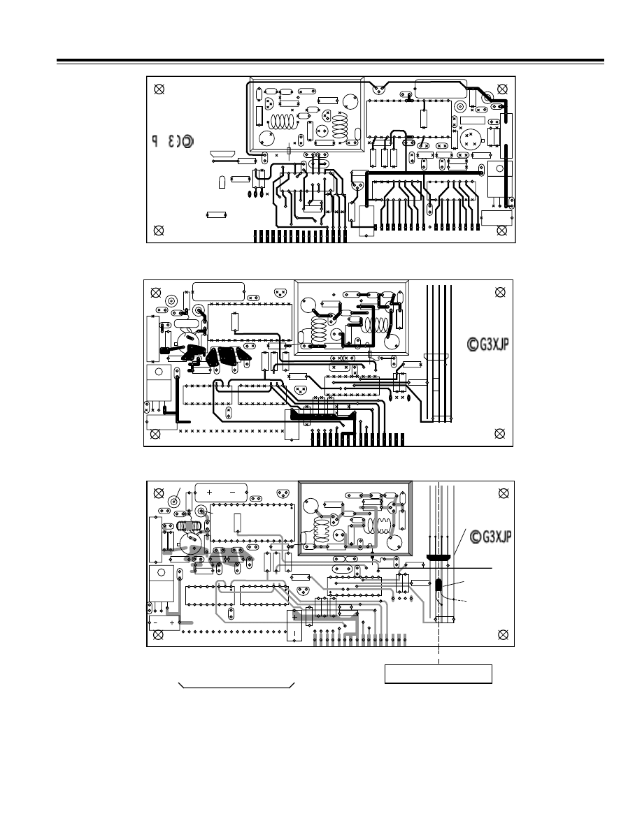
–21–
AN-557
REV. 0
Figure 14. DDS board PCB drawn for production using same conventions as Figure 12. All holes are 0.7 mm dia except three
leads from IC2 which are 1 mm. Ref oscillator is screened by PCB enclosure. C7 uses its leads to connect from tap on L2, via
hold in enclosure to top track. C1 is connected to track via short jumpers. IR detector/diode and disc shown for mounting at
90 degrees to display to top track. C1 is connected to track via short jumpers. IR detector/diode and disc shown for mounting
at 90 degrees to display board.
BOTTOM VIEW – (NON-COMPONENT SIDE) SHOWING BOTTOM TRACK AND SOLDERING POINTS
TOP VIEW – (COMPONENT SIDE) SHOWING TOP TRACK AND SOLDERING POINTS
18MHz
C17
RA0
RA1
RA2
RA4
RA3
5V
C20
12V
R17
C15
IC1
RFOUT
R33
R16
R15
TR3
T1
C22
IC2
C16
C8
6.1" x 2.75"
C19
C28
C26
C24
R11
R12
C23
C27
C25
C12
R7
R28
DDS ASSY
COMPRISING
IC4, R9, R10,
R18, C14
C9
R32
R26
R25
R24
D2
R23
IC3
PROGRAMMER
INTERFACE
ONLY
MCLR
RB7
0V
RB6
DIRECTION
PULSE
R19
DIODE
ANODE
D1
IR DETECTOR
IC5
R20
R21
C18
C13
X2
R31
R30
SLOTTED DISC
51MM DIA
C30
C29
TR4
R22
R8
R27
R29
C10
R13
C21
L4
L3
C7
TC2
R6
X1
C33
C31
R4
R3
TR1
L1
L2
R2
TC1
R1
C3
R5
C32
C6
C5
C4
C2
15MHz
14MHz
29MHz
28MHz
24MHz
21MHz
10MHz
0V
USE CW IF
USE USB IF
USE LSB IF
7MHz
3.5MHz
1.8MHz
BROADBAND
[SPARE]
T/R (PTT LINE)
RB1
RB2
RB3
RB0
RB5
0V
SHAFT CENTER LINE
TUNING KNOB
(NOMINALLY 1.75" DIA)
LOGIC INTERFACE TO Tx/Rx
NB ALL TRACKS MARKED 0V
ARE CONNECTED TO
THE GROUND PLANE
TOP VIEW – SHOWING COMPONENT LOCATION AND DRILLING TEMPLATE
5V
0V
IC6
IC7
C11
C1

REV. 0
–22–
AN-557
PART 5 OF 5
In this concluding article, the process for calibration is
covered. Suggestions for operational use are also
offered together with a complete definition of the key-
pad sequences and the resulting system behavior.
CALIBRATION PROCESS
Because the software has been explicitly written to
handle a range of different reference oscillator crystal
frequencies; and the use of any IF in the HF range (in-
cluding 0 for direct conversion) there is a calibration
process which stores the details of your installation in
long term memory.
You will need to follow this process on first use, any
time you change your Tx/Rx installation and then
periodically, thereafter, to compensate for any crystal
ageing.
There are two separate procedures, namely first cali-
brating the reference oscillator; and then calibrating up
to three IF offsets (USB, LSB, CW). They are both con-
ducted with the synthesizer connected to its mixer in the
target Tx/Rx and with everything warmed up and with a
reasonable ambient room temperature.
On first use, the general idea is to get the calibration
roughly right (i.e., within a few kHz) against any crude
definition of frequency available to you; and then to get
it as good as you can against some known (and typically
off-air) standard.
A WORD OF CAUTION . . .
Any time you enter one of the calibration modes (by
pressing the “Cal” key) you must explicitly exit calibra-
tion mode before resuming normal use. There are only
two ways to do this. One way is to save the calibration
setting (931, 934, 937 or 933) and the other is to key
“999” for a complete restart. Use the latter if in any
doubt.
REFERENCE OSCILLATOR CALIBRATION
This process gives best results when carried out at the
highest possible frequency. In practice it is easiest to get
it roughly right at some low frequency and finalize it
against some HF standard such as WWV on 15 MHz.
On first use, the software is set for a 100 MHz reference
oscillator. This is the lowest permitted frequency and
was chosen to make for easy percentage arithmetic. For
example, if you are using a 116 MHz crystal, you will
actually generate frequencies roughly 16% higher than
that indicated. Roughly, because no two crystals oscilla-
tors will go off at the same frequency.
You will need a separate AM receiver tuned to a station
of known frequency. As an aide to getting started, PIC
“N” MIX memory locations are preloaded with BBC
World Service frequencies. These are not frequency
standards but can be found reliably throughout Europe
on a simple domestic radio with a short-wave band and
will provide basic calibration. Proceed as follows:
Set the synthesizer to indicate the target calibration
frequency.
Key “83” to enter signal generator mode. This mode
ignores all IF offsets (and therefore any offset calibra-
tion errors) and generates the indicated frequency plus
or minus only any calibration error.
Locate the generated frequency on your AM receiver.
You may need a small antenna attached to the synthe-
sizer output. On first use it is worth calculating where
the expected frequency will come out as the error can be
substantial (up to +20%).
Key “83” again to exit signal generator mode.
Key “33” to enter reference clock calibration mode. This
is the same as signal generator mode except that as you
turn the tuning knob the displayed frequency remains
fixed while the software reference oscillator trimmer is
varied —thus altering the emitted frequency.
Turn the tuning knob and check on the other receiver
that you are moving in the right direction. Then keep
turning until you get to the chosen calibration fre-
quency. The tuning is very fine, so you will be turning
for a long time if the error is large.
Zero beat with the frequency standard initially and key
“933” [Save Cal Cal] to retain this coarse calibration.
Now repeat and refine the calibration at the highest pos-
sible HF frequency against some known standard.
Here is a little trick to help. Since tuning for zero beat can
be a bit arbitrary, it is useful to set one VFO 200 Hz above
the calibration frequency and the other VFO
200 Hz below it. When you hold down the A/B key, it will
alternate between the two—and you can easily judge
if the two beat notes are the same—to within a few Hz.
Just take a second opinion, because a significant
percentage of the population is tone deaf—and don’t
know it!
The same trick can be extrapolated to fine tuning IF off-
set calibration.
IF OFFSET CALIBRATION
There is no point in doing this until the reference oscilla-
tor is immaculately calibrated. Or rather, any time you
alter the reference oscillator calibration, you must
repeat this offset calibration.

–23–
AN-557
REV. 0
This procedure lets the synthesizer know the exact fre-
quencies of your IF offsets for LSB, USB and CW (if
fitted). Remember to allow a modest time for crystal
warm-up if you are switching between carrier crystals
on the host.
If you are using direct conversion, either ignore this
procedure and simply use the synthesizer in signal
generator mode—or follow this procedure but enter 0
as the offsets. This applies equally if you are using the
PIC “N” MIX as a QRP Tx.
To make life easy on first use, the USB offset is loaded
with 10.7 MHz, the CW offset with 9 MHz and the LSB
offset with 455 kHz as representing the three common
choices. This may seem obtuse as none of these is correct
for anyone. But it does provide the quickest way to get it
right for most. On first use only then, choose the IF that
is nearest to yours and copy it across to the other two as
follows:
Key “3” followed by “1,” “4” or “7,” selecting your
desired offset from the choice of three.
Key “93” followed by “1,” “4” or “7” thereby overwriting
one unwanted offset.
Repeat to overwrite the other offset.
At this stage all the offsets are identical and at least in
the right part of the spectrum. Now proceed as follows:
Select your USB crystal on the Tx/Rx. This is the lower
frequency of the two sideband crystals.
Key “31” [Cal USB] and turn the tuning knob to zero
beat. At this point the frequency display will show your
offset frequency. When happy, key “931” [Save Cal
USB] to save the result—and reboot the synthesizer.
Select your LSB crystal on the Tx/Rx. This is the higher
frequency of the two sideband crystals.
Key “37” [Cal LSB] and turn the tuning knob to zero beat
followed by “937” [Save Cal LSB] as above.
Repeat the process for your CW crystal if you have one,
otherwise leave it in the centre of the IF passband.
IF offsets are calibrated to 10 Hz. If you want to be fussy,
you can actually trim the carrier crystals themselves by a
maximum of 5 Hz to get it exact. This will have abso-
lutely no effect on IF performance.
This completes the calibration process.
OPERATIONAL USE
If you have relied on a simple VFO up to now, then the
range of features provided may seem daunting at first
sight. There may indeed be some which turn out to be
not useful in your particular operational circumstances.
That is OK; simply ignore them. My general advice is to
try them all out to start with, while contemplating the
circumstances under which you would use them.
At the end of the day, you have 12 keys and a tuning
knob and it does not take long to become familiar with
using them in the right order!
KEYPAD SEQUENCES
Substantial effort has gone into the ergonomic design of
the keypad sequences to make them easy and safe to
use. A brief review of the design thinking will hopefully
make them more memorable. The key sequences are
listed in Table I for easy reference.
All key sequences are executed immediately. For visual
confirmation, the key sequence is displayed and held
briefly on the frequency readout. Any invalid sequence
simply has no effect.
Every attempt has been made to combine the key
legends into crude meaningful sentences. Obvious
examples already discussed are Cal USB (enter USB
calibrate mode) or Save Cal USB (save this frequency as
USB calibration).
A few critical operational functions are achieved with
one key press. Most normal functions require two key
presses with the most commonly used functions being
achieved with two presses of the same key.
The key sequences also have an up/down directional
theme. For example USB is above CW on the keypad
which in turn is above LSB.
All sequences of three keys begin with the “9” key
[Save]. This acts as a qualifier on the two key sequence
which follows. For example, “10” means go to 10 m.
Conversely ”910” means save the present frequency as
the 10 m default. The word “save” is always used here
to mean retain even while powered off.
AT SWITCH-ON
The system will initialize to 3.7 MHz until you change it.
To store and retain a new switch-on frequency, first go
to the desired frequency (by any means, see later) and
enter “990” [Save, Save, Zero]. This will save the start-
up frequency with full 10 Hz resolution. The sideband in
use at save time is not stored; and the system will
initialize to the “normal” one for that frequency.
BAND SWITCHING
TO CHANGE BANDS, key the first two digits of any one
of nine bands in meters. (e.g. “80” for 80 m, “10” for
10 m). The “nonexception” is Top Band (alas, no longer
Top) where you key “16” as per the above rule. The
synthesizer will immediately go to the initialization
frequency for that band and automatically select the
“normal” sideband. If fitted, the band switching and
sideband selection outputs to the host will change
automatically to correspond.

REV. 0
–24–
AN-557
If you are on USB or LSB at band switch time, the new
band will initialize to the “normal” sideband for that fre-
quency. If you are on CW, the new band will initialize on
CW.
To change the initialization frequency for any band, first
go to the desired frequency (by any means, see later)
and enter “9” [Save] followed by the 2-digit band se-
quence. This will save the frequency rounded down to
the nearest 1 kHz.
In fact, you may save any arbitrary frequency against
each 2-digit band code. For example, if you never use
some bands, you may save any useful frequency in their
2-digit allocations. And change them at will.
Specifically, the sideband and band switching outputs
are computed from the 10 MHz and 1 MHz digits of the
actual frequency and not from the 2-digit key sequence.
MANAGING TWO VFOs
Because this is the most useful and critical feature set,
all functions are achieved immediately with one key
press. There are three of them on the bottom row of the
keypad, from left to right:
A/B
Pronounced in full as “VFO A or VFO B.” This swaps be-
tween the two VFOs. Whichever one you are on, you will
switch to the other. In fact, both the frequency and the
mode associated with the VFO are swapped over. In this
context, mode is the sideband (i.e., USB/LSB/CW), dis-
play resolution (10 Hz or 100 Hz) and injection either
high or low side of the IF). Since the two VFOs may be on
nearby or vastly different frequencies, this gives a full
range of facilities from IRT or ITT through to cross-band
capability.
A = B
Sets both VFOs to the same frequency and mode,
namely the ones you are using at the moment of entry.
This is how the system is initialized at power-on—with
both VFOs the same.
This key is used to establish a known situation before
tuning around should you want to be able to revert
quickly to the original frequency (by pressing “A/B”)—
or if you want to use split working for IRT, etc.
Split
This toggles between split and pure transceive opera-
tion. The state of this setting is immediately apparent
from the LED indicators.
If you are operating “split” then the Rx VFO LED will be a
different color (red/green) to the Tx VFO LED. Con-
versely, on pure transceive, they are the same color.
In any event, the frequency readout always applies to
the current transmit/receive state. If you are on receive,
the receive frequency is shown; on transmit, the trans-
mit frequency.
DISPLAY RESOLUTION
By default, the 6-digit display starts with the most sig-
nificant digit on the far left with no leading zero, and
then fills the rest of the digits to the right. Decimal points
are placed after the MHz and kHz digits.
The consequence of this autoranging is that the right
hand digit gives 10 Hz resolution on frequencies below
10 MHz and 100 Hz resolution above 10 MHz.
If you want to suppress the 10 Hz digit below 10 MHz or
show it above 10 MHz then key “78” to toggle back and
forth—per VFO. The whole display moves along in the
appropriate direction, complete with decimal points and
if necessary, suppresses one leading zero.
USB/LSB/CW
THE “NORMAL’ SIDEBAND is selected automatically as
a function of displayed frequency when you switch
bands or go to a memory frequency. If you want to over-
ride this at any time or choose CW, press the USB, CW or
LSB key respectively, twice. The front panel LEDs will
confirm the change, the generated frequency will
change; but of course the displayed frequency itself will
not change. If you have not included the optional IF
selection outputs to your host Tx/Rx, you will have to
select the appropriate offset there manually.
The chosen offset is retained and associated with each
VFO when swapping VFOs.
NORMAL TUNING
TUNING AROUND is achieved—self evidently—by turn-
ing the tuning knob. Clockwise to increase frequency,
anticlockwise to decrease it.
This simple statement belies a number of intelligent tun-
ing algorithms which seek to establish your intent and
act to help.
With the specified shaft encoder disk, the natural tuning
rate is 3.6 kHz per rev. This is a little fast for easy netting
and far too slow for rapid frequency excursions. Accord-
ingly, the software monitors how fast you are turning
the knob—and for how long—and smoothly alters the
tuning rate between the extremes of
⬇1 kHz per rev
through to
⬇50 kHz per rev. If you want to monitor this
effect, especially while getting used to it, key “70” to
toggle on and off the LEDs as a bar-graph rate of tune
indicator.
At extreme turning rates (typically, a quick flick of the
wrist) a software flywheel engages automatically and
tuning continues in rapid 1 kHz steps in the chosen di-
rection with no further turning of the knob. All the LEDs
light when the flywheel is engaged.

–25–
AN-557
REV. 0
The slightest turn of the knob in the opposite direction
immediately cancels any outstanding frequency changes,
resets the tuning rate to minimum and cancels the
flywheel.
Equally, any transmit/receive switching or any key press
achieves the same effect instantly.
Operation of the flywheel may be toggled between
enabled and inhibited by keying “26.” It is enabled at
switch-on.
Since the synthesizer is continuously tunable over the
whole range, you could, in theory get to any frequency
by continuously turning the knob.
This is realistic for modest excursions if the flywheel is
engaged but in practice, large (>2 MHz) excursions are
best achieved using rate tuning or starting from the
nearest band or memory frequency; or entering the fre-
quency on the keypad.
For this reason and to maintain performance, the band
switch outputs to the host are not recomputed in normal
tuning mode unless the flywheel is engaged. Should
you find yourself tuning slowly across a band-edge
boundary and want to update the switching outputs,
simply force this by selecting (or reselecting) the desired
sideband.
UP AND DOWN 1 kHz
If you want to quickly tune to the nearest kHz point, key
“47” to round the frequency down to the nearest kHz —
or key “41” to round up to the nearest kHz.
RATE TUNING
In this mode the tuning knob controls not the frequency
but rather the rate of change of frequency. Thus, the
more you turn the knob clockwise, the faster the fre-
quency will increase. The more you turn the knob
anticlockwise, the faster the frequency will decrease.
Any change of direction will freeze the frequency
instantly. In this mode, the LEDs provide a bar-graph
display to show tuning rate.
To enter this mode, key “22” [Rate Rate]. The kHz deci-
mal point is pulsed to denote nonnormal tuning.
To exit, press any key or switch between transmit and
receive.
KEYPAD FREQUENCY ENTRY
Any frequency may be entered from the keypad to the
nearest kHz. To use this mode, key “88” [Freq Freq]. The
frequency display will blank, showing only the MHz and
kHz decimal points.
At this point you must now enter FIVE digits.
This implies entering a leading zero for frequencies below
10 MHz. For example, 1.812 MHz is entered as “01812.”
Conversely, 18.123 MHz is entered as “18123” and 181 kHz
is entered as “00181.” Immediately the fifth digit is en-
tered, the display auto-ranges, the output frequency is
generated, the “normal” sideband is selected, the front
panel LEDs are updated as are the band select and side-
band select outputs to the host.
If you make a mistake part way through, key either “*”
or “#” to abort the sequence and start again.
MEMORY OPERATION
Ten memories are provided, accessed from keys 60–69
[Mem 0–Mem 9]. These may be visualized simply as
quick jumps in frequency—much like band switching.
Having switched to a memory frequency, tuning proceeds
as normal from that frequency without altering the original
stored frequency.
To change the stored frequency, go to the desired new
frequency by any means and key “9” [Save] followed by
the two-digit memory code. For example, to store the
current frequency in memory location five, key “Save
Mem 5. Memory locations are stored with full 10 Hz
resolution.
SCANNING IN GENERAL
There are several scanning modes which share the
following features in common:
All are entered by a two-key sequence, the first key being
“5” [Scan]. All are exited to normal tuning mode by
pressing any key. Scanning stops immediately on
transmit/receive switching. If scanning and operating
“Split,” then the system reverts to pure transceive on
any transmit/receive change. While any scan mode is
engaged, the kHz decimal point is pulsed as a visual
reminder.
These scanning modes are useful not only for monitoring
activity in a number of different operational situations,
but are invaluable in adjusting band/high/low-pass
filters in signal generator mode.
SPOT FREQUENCY SCANNING
To switch continuously between two frequencies, first
place one VFO on each frequency. Then key “5*” [Scan
A/B]. Turn the tuning knob clockwise to increase the
switching delay and anticlockwise to decrease it. The
amount of delay is shown on the LED bargraph.
MEMORY SCANNING
To cycle between the ten memory locations, key “56”
[Scan Mem].
Again, the tuning knob controls switching delay.

REV. 0
–26–
AN-557
RANGE SCANNING
To scan across a range of frequencies, put one VFO at
each end of the range and then key “58” [Scan Freq].
You will then tune up from the low to the high limit,
switch back to the low limit—and repeat continuously.
At switch time, the line to the “RxA” LED is pulsed
briefly low and can be used to synchronize a “scope, etc.
The tuning knob now controls the frequency increments
and hence the tuning speed—as shown on the bar
graph. The display is dimmed in this mode to improve
performance.
GUARD CHANNEL SCANNING
To monitor a fixed frequency for activity—or lack of it —
while tuning elsewhere, first tune to the fixed frequency
(or guard channel). Then switch VFOs [A/B] and tune
around (or even switch bands), leaving the other VFO on
the guard channel.
Obviously, you can manually switch back and forth to
the guard channel at any time [A/B], but to do it auto-
matically key “55” [Scan Scan]. You may still tune on
the main VFO, but approximately every 20 seconds the
software will switch to the guard channel for about
one second and then switch back again. For perfor-
mance reasons, the flywheel is disabled on the main
VFO, but otherwise full normal tuning is available.
SELECT BROAD BAND
If the display frequency does not coincide with one of
the nine HF amateur bands, the band selection logic
automatically selects the “broad band” output. This is
so that you have the choice of using some different
front-end on your Rx. If you want to force this output,
then key “72” to toggle this output bit on and off.
SIGNAL GENERATOR MODE
In signal generator mode, the displayed frequency is
generated with no offsets. Key “83” to toggle signal
generator mode on and off. The “Sig Gen” LED provides
visual confirmation.
You may tune, switch bands and scan while still in
signal generator mode. The theoretical frequency range
of the DDS chip and control logic is from audio to half
the reference clock frequency. In practice, the LPF and
buffer amplifier limit this response at both ends of the
spectrum, so if you need the extremes, capacitively
couple an output from the DDS subassembly output pin
(Pin 19).
HI/LO SIDE INJECTION
By default, the synthesizer generates hi-side injection.
That is, wanted frequency plus intermediate frequency
offset. If you have a high IF and are on one of the higher
HF bands, the injection frequency is getting close to the
top limit for adequately suppressing unwanted birdies.
You may force lo-side injection any time by keying “87’
or hi-side injection by keying “81.” This choice is
retained with the VFO currently in use, so one option is
to have both VFOs on the same frequency, but one each
on hi/lo side injection.
The sideband selection outputs are switched to corre-
spond, so if all is setup and calibrated properly, you
should hear no perceptible shift in net frequency.
This feature is also useful if you have an asymmetric IF
filter since you may arrange to always use it on the same
sideband.
The facility is retained for flexibility since it may be
possible to use the synthesizer on 6 m with lo-side
injection into a high IF—or with HF transceivers using
up-conversion architectures. Neither of these possibili-
ties has been tried.
SLEEP MODE
This mode was included in development to determine if
the PIC and/or the multiplexed display was coupling any
noise into the DDS output. In Sleep mode, the PIC stops
executing the program so the displays and keypad are
effectively switched off and the DDS continues to gener-
ate the last commanded output. In my installation there
is no perceptible difference in noise on the DDS output
at any frequency.
The facility was retained because the substantial power
saving may be useful in some environments—and noise
is an insidious beast prone to appear unsolicited at
any time.
To enter Sleep mode key “73.” To exit Sleep mode, simply
turn the tuning knob.
IN CONCLUSION
Hopefully this article will have inspired you to upgrade
a conventional injection system. My intention in writing
it was to remove some of the mystique surrounding
“computers” by showing their place in a real-world
useful application. I look forward to reading about the
fruits of your labors in the near future.
ACKNOWLEDGMENTS
My thanks go to Jack, G3XKF who built the first production
prototype and suffered some of the early software. Jack
is also responsible for the photography and was good
enough to turn up the bushes for my shaft
encoder.
My thanks also to Keith, G3OHN who independently
designed and built something similar for his Third
Method transceiver Much useful mutual learning occurred
over the air. Also to David, G3LUB for his help with
spurious measurements.
And lastly, to my wife Fran who was reliably advised she
had seen the last project withthe third method transceiver.
–27–
AN-557
REV. 0
Table I. Summary of Two-Key Entries
First Key
⇒
1
2
3
4
5
6
7
8
Second Key
⇓
USB
Rate
Cal
CW
Scan
Mem
LSB
Freq
0
9 10 m
9 20 m
9 30 m
9 40 m
9 Mem 0
Bar Graph
9 80 m
on Tune
1
Select
9 Cal
Up 1 kHz
9 Mem 1
Hi Side
USB
USB offset
Injection
2
9 12 m
Tune Rate
9 Mem 2
Broad
Mode
Band
3
9 Cal Ref
9 Mem 3
Sleep
Sig Gen
Clock
Mode
Mode
4
9 Cal
Select CW
9 Mem 4
CW Offset
5
9 15 m
Guard
9 Mem 5
Channel
6
9 160 m
Flywheel
Scan
9 Mem 6
Disable
Memories
7
9 17 m
9 Cal
Down 1 kHz
9 Mem 7
Select LSB
Lo Side
LSB Offset
Injection
8
Scan Freq
9 Mem 8
Shift
Keypad
Display
Freq Entry
9
9 Mem 9
*
Scan VFOs
Note that the ergonomic beauty of the entries can only be visualized when looking at the keypad layout with overlay legends. Entries shown preceded
with a “9” save the current frequency in that location when the two-key entry is preceded by the “Save” [9] key. Other combinations are “990” which
saves the power-on frequency and “999” which restarts the software.
Figure 15. 180 slot encoder disc, 51 mm dia for repro-
duction on acetate film.
PRINTED IN U.S.A.
E3732
–
.5
–
4/00 (rev. 0)
Wyszukiwarka
Podobne podstrony:
J Pachelbel Canon in D (re) Organ transcription (score sheet)
CCD imaging in amateur and professional astronomy, ccd
audiovisual translation in amateur translation
Amateur Radio
J Pachelbel Canon in D (re) Organ transcription (score sheet)
uptodate2 in your dreams transcript
Transcendentalism in Movies
Albinoni Adagio In G Minor (Sol Minore) Organ Solo Transcription (Score Sheet)
alternatywne radio in london
AFV Interiors German AFV Radio Equipment In WWII
Burke Transcendence in Classical Samkhya
John Gregory Betancourt Sherlock Holmes In The Amateur Mendicant Society
Nature of bacterial colonization influences transcription of mucin genes in mice during the first we
Albinoni Adagio In G Minor (Sol Minore) Piano Transcription (Score Sheet)
Pager Handbook for the Radio Amateur
0253215757 Indiana University Press Transcendence in Philosophy and Religion Jun 2003
Pachelbel Canon In D (Guitar Transcription)
Albinoni Adagio In G Minor (Sol Minore) Organ Solo Transcription (Score Sheet)
radio jako medium audialne
więcej podobnych podstron