Philips Semiconductors
Interconnectivity
______________________________________________________________________________________________
Philips Semiconductors - Asia Product Innovation Centre
Visit
http://www.flexiusb.com
8 June 1998
Application Notes
Interfacing PDIUSBD12 to Hitachi H8S/2357

Interconnectivity
Page 2 of 3
Application Notes: Interfacing PDIUSBD12 to Hitachi H8S/2357
______________________________________________________________________________________________
Philips Semiconductors - Asia Product Innovation Centre
Visit
http://www.flexiusb.com
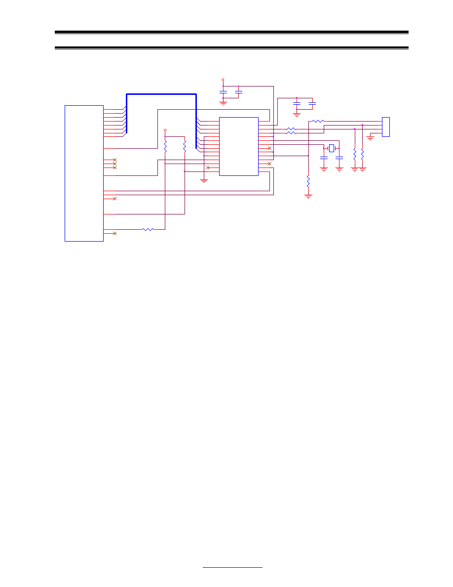
Example Interfacing Circuit in Non-DMA Mode
Above schematic shows interfacing PDIUSBD12 to H8S/2357 with minimum glue logic
components. The PDIUSBD12 works in non-DMA mode.
1. Interrupt Handling
Program the IRQ Sense Control Register (ISCRH and ISCRL) to specify low-level sense IRQ
input.
2. Address Mapping
The bus controller partitions the total 16Mbytes address space into eight areas, 0 to 7, in 2Mbytes
units. The bus controller will output CS0 to CS7 when external address space for each area is
accessed.
PDIUSBD12 can be mapped to any address area, where is simple for interfacing requirements.
In above example circuit, PDISUBD12’s base address is mapped to H’FFFF08 in CS7 area.
Assuming that it is the only external device within this area, CS7 can be directly connected to
CS_N.
The external bus specifications, bus width, number of access states and number of program wait
states, can be programmed for each area. Recommend setting for PDIUSBD12 are 8-bit bus in
Bus Width Control Register (ABWCR), enable wait states in Access State Control Register
(ASTCR) and 1 program wait states in Wait Control Register (WCRH and WCRL).
3. Using DMA
H8S/2357 can be programmed to single-address DMA to work with PDIUSBD12. In single
address DMA mode, the source and destination are accessed within the same read/write cycle.
But this doesn’t mean DMA transfer will be significantly faster than non-DMA, because the
transfer rate is also limited by USB bus maximum bulk transfer rate (1.152MBytes/S) and
PDIUSBD12 parallel bus interface speed (2MBytes/s).
VCC
VCC
R2
18
J1
USB_CON4B
1
2
3
4
C6
68P
R3
18
C5
22P
C2
0.1u
U2
PDIUSBD12
DATA0
1
DATA1
2
DATA2
3
DATA3
4
GND
5
DATA4
6
DATA5
7
DATA6
8
DATA7
9
ALE
10
CS_N
11
SUSPEND
12
CLKOUT
13
INT_N
14
RD_N
15
WR_N
16
DMREQ
17
DMACK_N
18
EOT_N
19
RESET_N
20
GL_N
21
XTAL1
22
XTAL2
23
VCC
24
D-
25
D+
26
VOUT3.3
27
A0
28
C1
470P
C4
1u
C3
0.1u
R4
47K
R5
10K
R1
4.7K
R8
1M
Y1
6MHz
R6
1M
R7
1M
U1
H8S/2357
D0
D1
D2
D3
D4
D5
D6
D7
A0
-DREQ0
-DACK0
-CS7
-RD
-LWR
-IRQ0
P1.0
-TEND
P1.1
-HWR
R9
4.7K

Interconnectivity
Page 3 of 3
Application Notes: Interfacing PDIUSBD12 to Hitachi H8S/2357
______________________________________________________________________________________________
Philips Semiconductors - Asia Product Innovation Centre
Visit
http://www.flexiusb.com
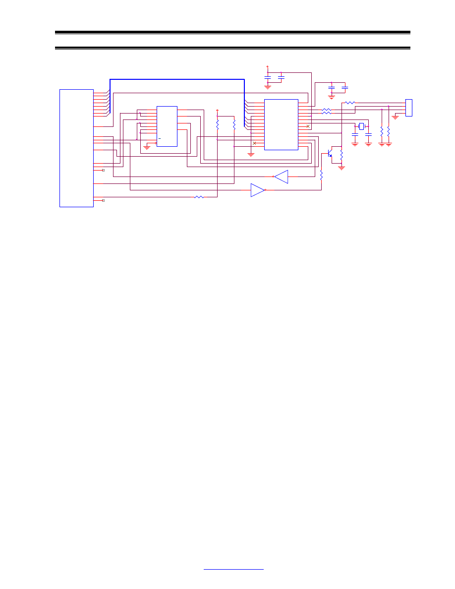
Above circuit shows single address mode DMA interface. A quad 2-input multiplexer, 74HC157,
is used to generate RD_N, WR_N and proper delay on DMACK_N to PDIUSBD12. DMREQ
needs to be inverted and TEND from H8S/2357 needs to be converted to an open collector
output.
4. I/O Ports
In example interfacing schematic, PDIUSBD12’s SUSPEND pin is connected to P1.0 which is
configured as a general input port by default. P1.0 may be configured to a general output port
when it is required to drive SUSPEND pin low during remote wake up.
The 4.7K resistor (R9) is added as protection against the faulty situation when P1.0 output high
and PDIUSBD12 pulls SUSPEND pin low.
There are 3 registers to configure port 1: Port 1 Data Direction Register (P1DDR), Port 1 Data
Register (P1DR) and Port 1 Register (PORT1).
VCC
VCC
R2
18
J1
USB_CON4B
1
2
3
4
C6
68P
R3
18
C5
22P
C2
0.1u
U2
PDIUSBD12
DATA0
1
DATA1
2
DATA2
3
DATA3
4
GND
5
DATA4
6
DATA5
7
DATA6
8
DATA7
9
ALE
10
CS_N
11
SUSPEND
12
CLKOUT
13
INT_N
14
RD_N
15
WR_N
16
DMREQ
17
DMACK_N
18
EOT_N
19
RESET_N
20
GL_N
21
XTAL1
22
XTAL2
23
VCC
24
D-
25
D+
26
VOUT3.3
27
A0
28
C1
470P
C4
1u
C3
0.1u
R4
47K
R5
10K
R1
4.7K
R8
1M
R10
1K
Y1
6MHz
R6
1M
R7
1M
U4A
74HC04
1
2
U3
74HC157
1A
2
1B
3
2A
5
2B
6
3A
11
3B
10
4A
14
4B
13
A/B
1
G
15
1Y
4
2Y
7
3Y
9
4Y
12
U4B
74HC04
3
4
Q1
NPN
R9
1M
U1
H8S/2357
D0
D1
D2
D3
D4
D5
D6
D7
A0
-DREQ0
-DACK0
-CS7
-RD
-LWR
-IRQ0
P1.0
-TEND
P1.1
-HWR
Document Outline
Wyszukiwarka
Podobne podstrony:
PDIUSBP1
PDIUSBP1
PDIUSBH11A KEYBOARD APPLICA
PDIUSBH11A APPNOTES
PDIUSBD11 KEYBOARD MOUSE
PDIUSBH11A KBD APPNOTES
PDIUSBD12 HITACHI H8S 2357
PDIUSBH11A APPLICATION NOTE
PDIUSBH11A H12 FIRMWARE
więcej podobnych podstron