7
9
25274 75349
1 1>
CIRCUIT
CELLAR
®
www.circuitcellar.com
T H E M A G A Z I N E F O R C O M P U T E R A P P L I C AT I O N S
$4.95 U.S. ($5.95 Canada)
#160 November 2003
EMBEDDED DEVELOPMENT
Mixed-Signal Simulator
All-Digital Amplifier
Efficient Menu System
Future of FPGA

Now with
instrumentation-quality
programmable analog.
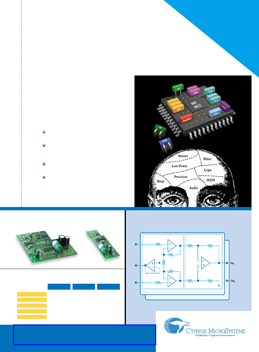
Powerful new programmable analog and digital
blocks with memory and MCU for less than $2.
Winner of the EDN Innovation of the Year award,
our PSoC
TM
Programmable System-on-Chip
TM
device
is changing the face of embedded design.
Replace 1,000s of fixed-function devices
with a couple of keystrokes
Dynamically reconfigure a PSoC device,
changing functionality on the fly in any
application
Select from hundreds of predefined
blocks in our mixed-signal library
Already designed into 1,000s of applications;
check out our online app note library
PSoC
™
Mixed-Signal Array.
It’ll change the way you
think about embedded design.
Instrumentation Amp with Driven Shield
Front End with Adjustable Gain
Difference Amp
Instrumentation Amp 2
CYPRESS ENHANCED ANALOG
™
(CEA
™
)
•
Rail-to-rail analog
•
Instrumentation amps
•
Lower voltage offset
•
Lower input leakage currents
•
Programmable gains
•
Better stability
One of 1,000s of examples of programmable analog blocks.
PSoC Mixed-Signal Arrays with M8 Microcontroller
CY8C27X
CY8C24X
CY8C22X
126
3
8
4
4
16K
4K
2K
256
256
256
low as $1.99
low as 99¢
low as 69¢
CEA ANALOG BLOCKS
DIGITAL BLOCKS
HI REL SONOS FLASH
SRAM
COST
Reduce board size and BOM up to 80%
before
after
Check out our free online training and our 4-hour applications support:
w w w . c y p r e s s . c o m / a d / p s o c - c e a 1
$30,000
PSoC International
Design Contest
w w w. c y pr es s . c o m
/a d /p s o c - c e a1
©
Cypress
Microsystems,
Inc.
2003.
PSoC,
Programmable
System-on-Chip,
Cypress
Enhanced
Analog
and
CEA
are
trademarks
of
Cypress
Microsystems,
Inc.
All
other
trademarks
are
the
property
of
their
respective
owners.
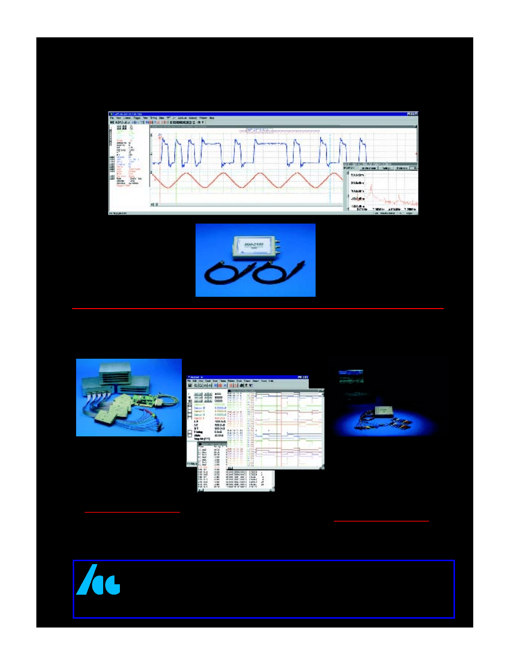
Digital Oscilloscopes
•
2 Channel Digital Oscilloscope
•
100 MSa/s
max single shot rate
•
32K samples per channel
•
Advanced Triggering
•
Only 9 oz and 6.3” x 3.75” x 1.25”
•
Small, Lightweight, and Portable
•
Parallel Port
interface to PC
•
Advanced Math options
•
FFT Spectrum Analyzer options
DSO-2102S
$525
DSO-2102M
$650
Each includes
Oscilloscope
,
Probes, Interface Cable, Power
Adapter, and software for
Win95/98, WinNT, Win2000
and DOS.
•
40 to 160 channels
•
up to 500 MSa/s
•
Variable Threshold
•
8 External Clocks
•
16 Level Triggering
•
up to 512K samples/ch
•
Optional Parallel Interface
•
Optional 100 MSa/s Pattern Generator
LA4240-32K (200MHz, 40CH)
$1350
LA4280-32K (200MHz, 80CH)
$2000
LA4540-128K (500MHz, 40CH)
$1900
LA4580-128K (500MHz, 80CH)
$2800
LA45160-128K (500MHz, 160CH)
$7000
Logic Analyzers
• 24 Channel Logic Analyzer
• 100MSa/S max sample rate
• Variable Threshold Voltage
• Large 128k Buffer
• Small, Lightweight and Portable
• Only 4 oz and 4.75” x 2.75” x 1”
• Parallel Port Interface to PC
• Trigger Out
• Windows 95/98 Software
LA2124-128K (100MSa/s, 24CH)
Clips, Wires, Interface Cable, AC
Adapter and Software
$800
All prices include Pods and Software

E
ach year, we use the Embedded Development issue to feature the
newest methods and tools used to design hardware and software. This
month, we have a variety of compelling articles about developing embed-
ded applications.
When you’re working with both analog and digital signals, simulation
can get complicated if you have to handle the signals separately. But, what
if you could simultaneously simulate both parts? Engin Ipek and Bruce
Land explain how to build a mixed-signal simulator that you can use to
gather analysis for display on a monitor (p. 14). The simulator was origi-
nally designed for use with small Atmel AT90S8515-based projects, but the
source code can be modified to work with multiple processors.
Aubrey Kagan provides a solution to another problem (p. 44). In
embedded systems, space is often critical. By carefully organizing hierar-
chal menus, Aubrey devised a way to reuse software for displaying and
changing parameters in order to save ROM space. This is especially use-
ful when your client’s requirements change; with a flexible menu, you can
simply alter the flow of the hierarchy to modify the program.
This month, we’re also showcasing the winners of the Motorola Flash
Innovation 2003 Design Contest (p. 22). The contestants worked with the
HC08 Q-Family to develop a number of unique and exciting projects. For
those of you who are interested in reading more about the winning
designs, we have posted dozens of abstracts and full entries on our web
site (www.circuitcellar.com/fi2003).
While you’re on the web site, you should also take the opportunity to
check out the revised Author’s Guide (www.circuitcellar.com/authors). With
the editorial calendar, you will find definitions of our monthly themes and
suggestions for article topics. The issues fill up quickly, so it’s a good idea
to send in your proposals as early as possible. (Note that the deadlines are
for final materials. Proposals should be submitted in advance.)
2004 Editorial Calendar
Issue
Theme
Deadline
January
Analog Techniques
October 1
February
Wireless Communication
November 3
March
Embedded Applications
December 1
April
Robotics
January 2
May
Communications
February 2
June
Measurement & Sensors
March 1
July
Graphics & Video
April 1
August
Embedded Programming
May 3
September
Signal Processing
June 1
October
Data Acquisition
July 1
November
Internet & Connectivity
August 2
December
Embedded Development
September 1
4
Issue 160 November 2003
www.circuitcellar.com
CIRCUIT CELLAR
®
EDITORIAL DIRECTOR/FOUNDER
Steve Ciarcia
MANAGING EDITOR
Jennifer Huber
TECHNICAL EDITOR
C.J. Abate
WEST COAST EDITOR
Tom Cantrell
CONTRIBUTING EDITORS
Ingo Cyliax
Fred Eady
George Martin
George Novacek
Jeff Bachiochi
NEW PRODUCTS EDITOR
John Gorsky
PROJECT EDITORS
Steve Bedford
Ken Davidson
David Tweed
ADVERTISING
PUBLISHER
Dan Rodrigues
E-mail: dan@circuitcellar.com
ASSOCIATE PUBLISHER/DIRECTOR OF SALES
Sean Donnelly
Fax: (860) 871-0411
(860) 872-3064
E-mail: sean@circuitcellar.com
Cell phone: (860) 930-4326
ADVERTISING COORDINATOR
Valerie Luster
Fax: (860) 871-0411
(860) 875-2199
E-mail: val.luster@circuitcellar.com
ADVERTISING ASSISTANT
Deborah Lavoie
Fax: (860) 871-0411
(860) 875-2199
E-mail: debbie.lavoie@circuitcellar.com
CONTACTING CIRCUIT CELLAR
SUBSCRIPTIONS:
INFORMATION: www.circuitcellar.com or subscribe@circuitcellar.com
To Subscribe: (800) 269-6301, www.circuitcellar.com/subscribe.htm, or
subscribe@circuitcellar.com
PROBLEMS: subscribe@circuitcellar.com
GENERAL INFORMATION:
TELEPHONE: (860) 875-2199 Fax: (860) 871-0411
INTERNET: info@circuitcellar.com, editor@circuitcellar.com, or www.circuitcellar.com
EDITORIAL OFFICES: Editor, Circuit Cellar, 4 Park St., Vernon, CT 06066
NEW PRODUCTS: New Products, Circuit Cellar, 4 Park St., Vernon, CT 06066
newproducts@circuitcellar.com
AUTHOR CONTACT:
E-MAIL: Author addresses (when available) are included at the end of each article
CIRCUIT CELLAR®, THE MAGAZINE FOR COMPUTER APPLICATIONS (ISSN 1528-0608) and Circuit Cellar Online are pub-
lished monthly by Circuit Cellar Incorporated, 4 Park Street, Suite 20, Vernon, CT 06066 (860) 875-2751. Periodical rates paid at
Vernon, CT and additional offices. One-year (12 issues) subscription rate USA and possessions $21.95, Canada/Mexico
$31.95, all other countries $49.95. Two-year (24 issues) subscription rate USA and possessions $39.95, Canada/Mexico
$55, all other countries $85. All subscription orders payable in U.S. funds only via VISA, MasterCard, international postal money
order, or check drawn on U.S. bank.
Direct subscription orders and subscription-related questions to Circuit Cellar Subscriptions, P.O. Box 5650, Hanover, NH
03755-5650 or call (800) 269-6301.
Postmaster: Send address changes to Circuit Cellar, Circulation Dept., P.O. Box 5650, Hanover, NH 03755-5650.
For information on authorized reprints of articles,
contact Jeannette Ciarcia (860) 875-2199 or e-mail jciarcia@circuitcellar.com.
Circuit Cellar® makes no warranties and assumes no responsibility or liability of any kind for errors in these programs or schematics or for the
consequences of any such errors. Furthermore, because of possible variation in the quality and condition of materials and workmanship of read-
er-assembled projects, Circuit Cellar® disclaims any responsibility for the safe and proper function of reader-assembled projects based upon or
from plans, descriptions, or information published by Circuit Cellar®.
The information provided by Circuit Cellar® is for educational purposes. Circuit Cellar® makes no claims or warrants that readers have a right to
build things based upon these ideas under patent or other relevant intellectual property law in their jurisdiction, or that readers have a right to
construct or operate any of the devices described herein under the relevant patent or other intellectual property law of the reader’s jurisdiction.
The reader assumes any risk of infringement liability for constructing or operating such devices.
Entire contents copyright © 2001 by Circuit Cellar Incorporated. All rights reserved. Circuit Cellar and Circuit Cellar INK are registered trademarks
of Circuit Cellar Inc. Reproduction of this publication in whole or in part without written consent from Circuit Cellar Inc. is prohibited.
CHIEF FINANCIAL OFFICER
Jeannette Ciarcia
CUSTOMER SERVICE
Elaine Johnston
ACCOUNTANT
Jeff Yanco
ART DIRECTOR
KC Prescott
GRAPHIC DESIGNER
Mary Turek
STAFF ENGINEER
John Gorsky
QUIZ COORDINATOR
David Tweed
Cover photograph Chris Rakoczy—Rakoczy Photography
PRINTED IN THE UNITED STATES
Tools and Techniques of the Trade
jennifer.huber@circuitcellar.com
TASK MANAGER

6
Issue 160 November 2003
CIRCUIT CELLAR
®
www.circuitcellar.com
November 2003: Embedded Development
Flash Innovation 2003 Design Contest Winners
Announcement
Timing (Analysis) is Everything
A How-To Guide for Timing Analysis
Philip Nowe
Build An All-Digital Amplifier
Yoon Cho, Joe Huntley, Greg Nuttall, Bryan Olson, &
Derek Richardson, edited by David Tweed
Hierarchical Menus in Embedded Systems
High-Temperature Superconductor Overview
Programming the 386 in 32-Bit Protected Mode
OOPic Eases Programming Headaches
TASK MANAGER
Tools and Techniques of the Trade
PRIORITY INTERRUPT
Internet Infamy
FEATURES
COLUMNS
DEPARTMENTS
Check out AVR today at www.atmel.com/ad/fastavr
Introducing the Atmel AVR
®
. An 8-bit MCU that
can help you beat the pants off your competition.
AVR is a RISC CPU running single cycle instructions.
With its rich, CISC-like instruction set and 32 working registers,
it has very high code density and searingly fast execution–up to
16 MIPS. That’s 12 times faster than conventional 8-bit micros.
We like to think of it as 16-bit performance at an 8-bit price.
With up to 128 Kbytes of programmable Flash and EEPROM,
AVR is not only up to 12 times faster than the MCU you’re using
now. It’s probably 12 times smarter, too.
And when you consider that it can help slash months off your
development schedule and save thousands of dollars in project
cost, it could make you look pretty smart, too.
AVR comes in a wide range of package and performance
options covering a huge number of consumer and industrial
applications. And it’s supported by some of the best development
tools in the business.
So get your project started right. Check out AVR today at
www.atmel.com/ad/fastavr. Then register to qualify for your free
evaluation kit and bumper sticker. And get ready to take on the world.
Our AVR microcontroller is
probably 12 times faster than
the one you’re using now.
(It’s also smarter.)
AVR 8-bit RISC Microcontrollers
© 2002 Atmel Corporation. Atmel and the Atmel logo are registered trademarks of Atmel Corporation.
8
Issue 160 November 2003
CIRCUIT CELLAR
®
www.circuitcellar.com
Edited by John Gorsky
NEW PRODUCT NEWS
LOW-COST SDK FOR BLUESTREAK ARM9-BASED SoC
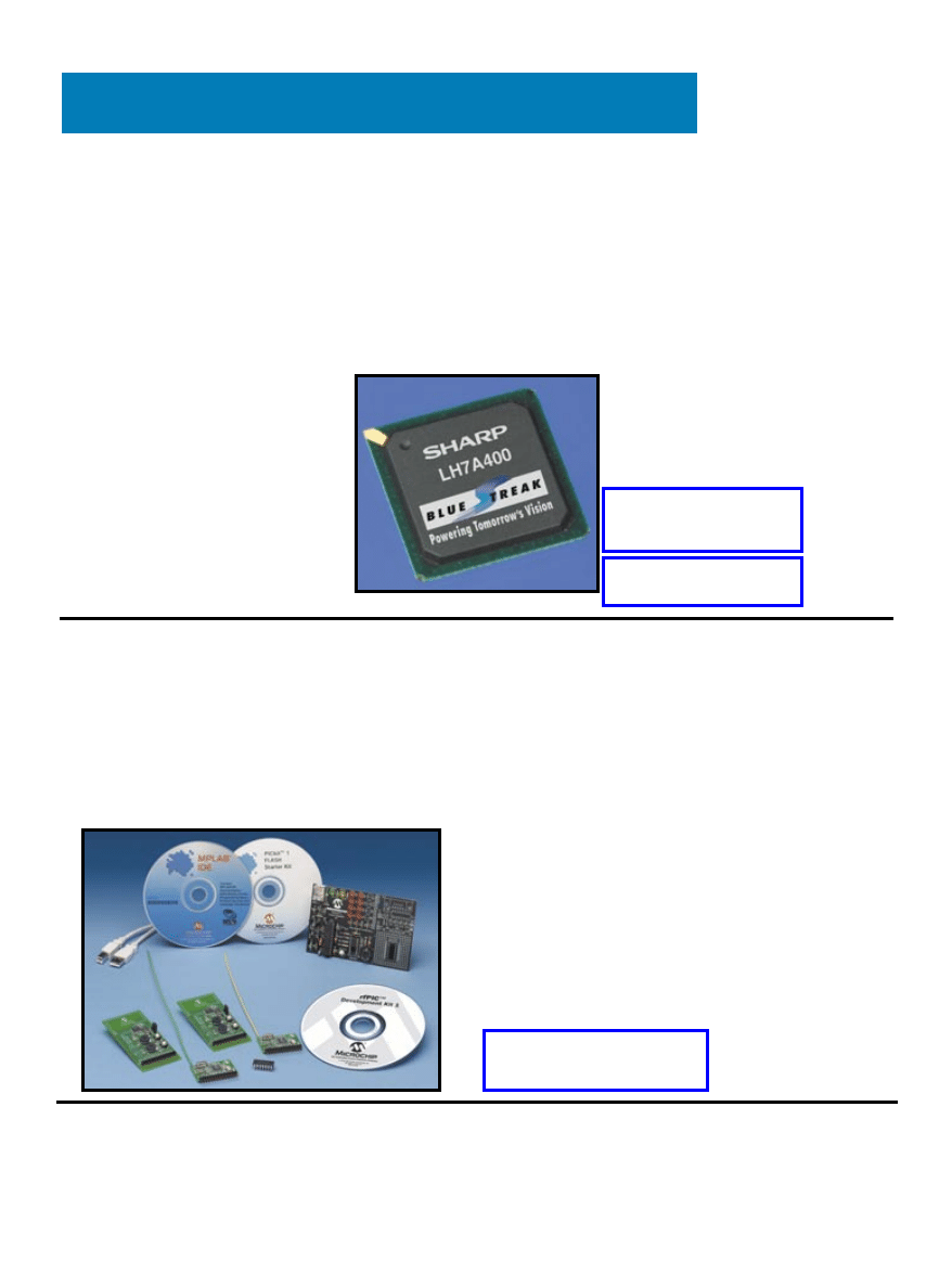
The LH7A400 Zoom SDK is a complete hardware and
software solution, enabling developers to immediately
begin developing applications and evaluating the function-
ality of the Sharp LH7A400 SoC and Card Engine (embed-
ded-computing module). The SDK simplifies development
by providing production quality software (device drivers
and bootloader) and binary board support packages for
Windows CE and Linux. It also provides optional display
kits that can be immediately connected to the develop-
ment kit, as well as expansion headers that provide easy
access to all of the Card Engine periph-
erals for application development, proto-
typing, and debugging.
The compact LH7A400 Card Engine is
a product-ready embedded-computing
module that offers the essential features
for handheld and embedded-networking
applications in the industrial, consumer,
and medial markets. The Card Engine
comes standard with the following hard-
ware: an LH7A400 ARM922T SoC run-
ning at 200 MHz, on-board flash memo-
ry (up to 32 MB), SDRAM (up to 64 MB),
a touchscreen controller, and a
10/100BaseT Ethernet controller. It also includes audio
codec, CompactFlash, and MCU-specific peripherals (e.g.,
an integrated LCD controller, USB client, I
2
C,
PCMCIA/CF, and RTC).
The LH7A400 is a highly integrated general-purpose
SoC that’s based on an industry-standard ARM9 core. It’s
specifically designed to meet the performance, power con-
sumption, and cost requirements of engineers designing
multimedia and mobile handheld applications. The starter
kit developed for the BlueStreak LH7A400 SoC is designed
to scale with the OEM’s product
roadmap. You can seamlessly plug
Sharp’s next-generation BlueStreak
MCUs and SoCs into the same applica-
tion board. The Zoom Starter
Development Kit for Sharp’s BlueStreak
LH7A400 costs $349.
Logic Product Development
(612) 672-9495
www.logicpd.com
Sharp Microelectronics
www.sharpsma.com
STATEMENT REQUIRED BY THE ACT OF AUGUST 12, 1970, TITLE 39, UNITED STATES CODE SHOWING THE OWNERSHIP, MANAGEMENT AND CIRCULATION OF CIRCUIT CELLAR, THE MAGAZINE FOR COMPUTER APPLICATIONS, published monthly at 4 Park
Street, Vernon, CT 06066. Annual subscription price is $21.95. The names and addresses of the Publisher, Editorial Director, and Managing Editor are: Publisher, Daniel Rodrigues, 4 Park Street, Vernon, CT 06066; Editorial Director, Steven Ciarcia, 4 Park Street, Vernon, CT
06066; Managing Editor, Jennifer Huber, 4 Park Street, Vernon, CT 06066. The owner is Circuit Cellar, Inc., Vernon, CT 06066. The names and addresses of stockholders holding one percent or more of the total amount of stock are: Steven Ciarcia, 4 Park Street, Vernon, CT
06066. The average number of copies of each issue during the preceding twelve months is: A) Total number of copies printed (net press run) 24,890; B) Paid/Requested Circulation (1) Mail subscriptions: 13,908; (3) Sales through dealers and carriers, street vendors and counter
sales: 5,871 C) Total paid circulation: 19,779; D) Free distribution by mail (samples, and other free issues): 208; E) Free distribution outside the mail (carrier, or other means): 763; F) Total free distribution: 971; G) Total Distribution: 20,750; H) Copies not distributed: (1) Office use
leftover, estimated newsstand returns, spoiled after printing: 4,140; I) Total: 24,890. Percent paid and/or requested circulation: 95.32%. Actual number of copies of the single issue published nearest to filing date is October 2003, Issue #159; A) Total number of copies printed (net
press run) 24,040; B) Paid/Requested Circulation (1) Mail subscriptions: 12,040; (3) Sales through dealers and carriers, street vendors and counter sales: 6,648; C) Total paid circulation: 18,688; D) Free distribution by mail (samples, and other free issues): 211; E) Free distribution
outside the mail (carrier, or other means): 861; F) Total free distribution: 1,072; G) Total Distribution: 19,760; H) Copies not distributed: (1) Office use leftover, estimated newsstand returns, spoiled after printing: 4,280; I) Total: 24,040. Percent paid and/or requested circulation:
94.58%. I certify that the statements made by me above are correct and complete. Daniel Rodrigues, Publisher.
MODULAR rfPIC DEVELOPMENT TOOL
The rfPIC Development Kit 1 provides you with an easy
way to evaluate low-power RF communication links for
embedded-control applications based on the rfPIC12F675
microcontroller plus an UHF RF transmitter and the
rfRXD0420 receiver device.
Designed to work in tandem with the popular PICkit 1
Flash Starter Kit, the rfPIC Development Kit 1 consists of
transmitter and receiver modules supporting the 315- and
433-MHz frequencies. The receiver modules, featuring the
rfRXD0420 device, plug directly into the PICkit 1 develop-
ment board for demonstration and development. All of the
design files are available, offering you the ability to
migrate the module design into the application for lower-
cost volume production.
Target applications for the rfPIC family of products
include the following: remote control (e.g., home appli-
ances, fan control, light control, and PC peripherals); com-
mand and control (e.g., air conditioning thermostats and
water irrigation systems); wireless sensors (e.g., tempera-
ture, smoke detectors, and water level); home security
(e.g., garage door openers and remote infrared sensors); and
automotive (e.g., tire pressure sensors, remote control, and
remote keyless entry).
Available with 315/433-MHz amplitude shift keying,
the rfPIC receiver module costs $25. The rfPIC transmitter
module costs $30. For $135, you can purchase a kit that
includes two receivers, two transmitters, and the PICkit 1
Flash Starter Kit.

NEW PRODUCT NEWS
10
Issue 160 November 2003
CIRCUIT CELLAR
®
www.circuitcellar.com
NIOS DEVELOPMENT KIT
The Nios Development Kit (Stratix Professional
Edition) features the largest FPGA available in a Nios
development kit, greater on-chip memory, increased
debug features, and newly bundled debugging software.
The kit’s Stratix FPGA provides resources to support the
development of complex, high-performance designs, and
the increased debug features and bundled software accel-
erate the development of systems based on the soft Nios
embedded-processor core.
The development kit
includes the latest release
of the Nios embedded
processor, V. 3.02, and the
Stratix EP1S40 device. The
development board features
16 MB of SDRAM, 1 MB of
SRAM, 8 MB of flash mem-
ory, a 10/100 Ethernet port,
two serial ports, and a
Mictor connector for soft-
ware trace debugging.
Furthermore, it includes
two expansion headers
(with more than 80 avail-
able user-defined I/O pins), a power supply, and a
ByteBlaster II download cable. The Nios processor also
contains the enhanced on-chip instrumentation (OCI)
core and software provided by First Silicon Solutions
(FS2) for real-time software debugging.
The development kit includes the Quartus II design
software and a complete suite of software development
tools. Bundled tools include Red Hat’s GNUPro compil-
er and GDB/insight debugging
tool, as well as evaluation ver-
sions of Accelerated
Technology’s Nucleus RTOS and
the code/lab Developer Suite,
which offers native support for
FS2’s BlackBox debug probe and
support for Altera’s ByteBlaster II
download cable for software
debug. The Nios Development
Kit (Stratix Professional Edition)
costs $2495.
www.circuitcellar.com
CIRCUIT CELLAR
®
Issue 160 November 2003
11
NEW PRODUCT NEWS
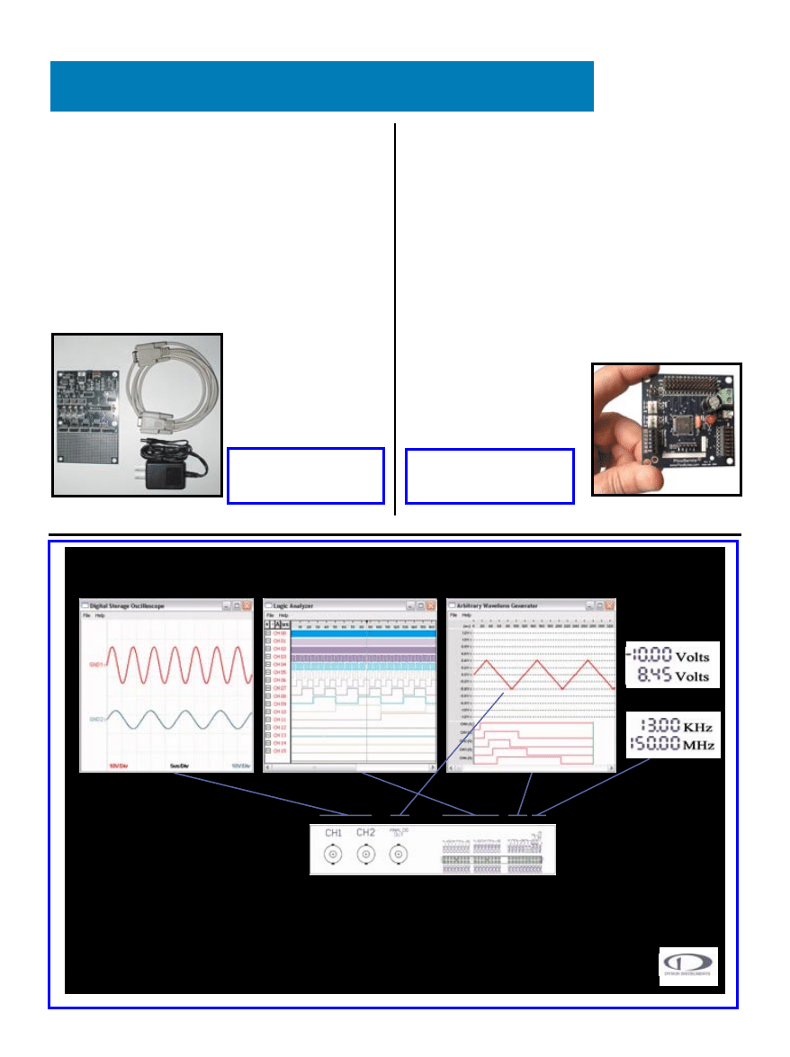
– 2 Channels, 5mV/Div to 20V/Div, 50nS/Div to 100mS/Div, Up to 80MSPS
– 1 Analog Output, 5 Digital Outputs, Up to 80MSPS
– 16 Channels, Multiple Trigger Options, Up To 80MSPS
Two Programmable Power Supplies
Dynon Instruments
Introduces the
PSoC EVALUATION KIT
The PSoC Evaluation Kit is a flexible evaluation sys-
tem that allows easy interfacing with the included PSoC
chip. The kit is easily integrated for use in embedded
systems. The 28-pin PSoC chip is socketed to allow for
the insertion of the ICE pod foot from the Cypress PSoC
Designer development kit for full in-circuit emulation.
In-system serial programming connectors are provided
for both the Cypress ISSP interface and the Arista
Systems RS-232 Serial PSoC Programmer.
Included are a precision analog interface, an RS-232
port, a precision oscillator, and in-system serial program-
ming. The kit also features an input voltage range of 7 to
30 VDC, a 9-VDC wall-
mount power supply,
headers for all of the
available I/O, and a large
prototyping area. The
PSoc Evaluation Kit
costs $199. Custom ver-
sions are available.
McGilvra Engineering
(517) 783-2623
www.mcgilvra.com
SERIAL R/C SERVO AND I/O CONTROLLER
The PicoServio (or Servio) is an intelligent serial R/C
servo and I/O slave controller capable of controlling up to
20 R/C servos with 16-bit resolution and 256 speed set-
tings. It has eight A/D converter ports capable of 10-bit
resolution at 40 samples per second. The controller has
two PWM signal generators capable of up to 10-bit resolu-
tion with direction control for H-Bridge connections. Any
unused A/D or servo ports can be configured as digital I/O.
The Servio offers powerful features such as monitoring
and sweep commands that offload the burden of constant
polling and control from the master CPU. An included
comprehensive user and technical manual explains all
aspects of operation and provides code examples.
The Servio consumes less than 14 mA and weighs only
0.8 oz. (22 grams) in a 2.5
″
×
2.5
″
(63 mm × 63 mm) foot-
print, which makes it ideal
for battery and mobile opera-
tions. PicoServio costs
$99.95.

12
Issue 160 November 2003
CIRCUIT CELLAR
®
www.circuitcellar.com
LOW-COST, 900-MHZ TRANSCEIVER
The 9XCite is a low-cost, FCC-approved, 900-MHz
wireless OEM module. The module breaks the low-cost
pricing barrier while providing long-range wireless to
OEMs with no configuration required.
The 9XCite module has a 1-mW power output. It is pin-
for-pin and software-compatible with MaxStream’s 100-
mW 9XStream 900-MHz transceiver. With OEMs, only
one interface needs to be designed to integrate wireless
links of various power
requirements into
applications.
This high-perform-
ance transceiver boasts
a –10-dBm receive sen-
sitivity providing
extended transmission.
The high-receiver sensi-
tivity allows the 9XCite
to compete with mod-
ules operating at 10
times the power output.
The 9XCite communi-
cates 300
′
(90 m)
indoors and in urban
environments, and 1000
′
(300 m) line-of-sight with dipole
antennas.
The 9XCite module accepts 2.85 to 5.50 VDC and is
optimized for low-power applications. Transmit and
receive current is less than 50 mA; power-down current
can operate as low as 20 µA. Data throughput is user-selec-
table at 9600 or 38,400 bps, and it provides interface data
rates from 1200 to 57,600 bps. Frequency hopping or sin-
gle-channel modes are
also user-selectable.
Support for RS-232 is
available for peer-to-peer,
point-to-point, point-to-
multipoint, and multidrop
networking topologies.
The 9XCite develop-
ment kit costs $199.
9XCite modules are avail-
able for $37 in quantities
of 1000.
MaxStream
(801) 765-9885
www.maxstream.net
NEW PRODUCT NEWS
www.circuitcellar.com
CIRCUIT CELLAR
®
Issue 160 November 2003
13
You may contact the quizmasters at eq@circuitcellar.com
CIRCUIT CELLAR
—
Test Y
Your E
EQ
Problem 2
—
What is the Curie point of a material?
Problem 3
—
How can this be used to regulate tem-
perature of, say, a soldering iron?
Problem 4
—
A certain kind of spectroscopy
requires that an AC voltage in the range of 1 to
25 kHz at 2 kV
RMS
be applied to a capacitive load of
about 1 nF. How much power does the power supply
need to deliver? How much current?
Contributed by David Tweed
Edited by David Tweed
Problem 1
—
While browsing some C code, you
come across an aaa.h file, which contains the follow-
ing lines:
GLOBAL int aaa_function1();
GLOBAL int aaa_function2();
The corresponding aaa.c file includes the following:
#define GLOBAL extern
#include "bbb.h"
#include "ccc.h"
#undef GLOBAL
#define GLOBAL
#include "aaa.h"
What is the purpose of the
GLOBAL
symbol?
view the contents of the memory and
the register file at each time step. It is
also possible to perform DC and tran-
sient analyses on the analog circuitry
and timing analysis on the logic compo-
nents (e.g., CMOS, TTL, etc.). An RS-
232 terminal emulator is implemented
to model communication using the
’8515’s UART. You have the ability to
edit models for new devices or change
certain parameters on the existing
devices. The results of the analog simu-
lation are output in an Excel file, and
the digital and RTL-level simulation
results can be viewed using GTKwave.
There are several devices that are pro-
vided by the simulator as library mod-
els: linear resistors and capacitors, ideal
and controlled sources, ideal op-amps,
diodes, and MOSFETs (Spice level 1
model) and Bipolar Junction Transistors
(BJTs). Noise sources, push-button
switches, logic gates and flip-flops,
AT90S8515 microcontrollers (at RTL
level), and the RS-232 terminal emula-
tor are also provided by simulator.
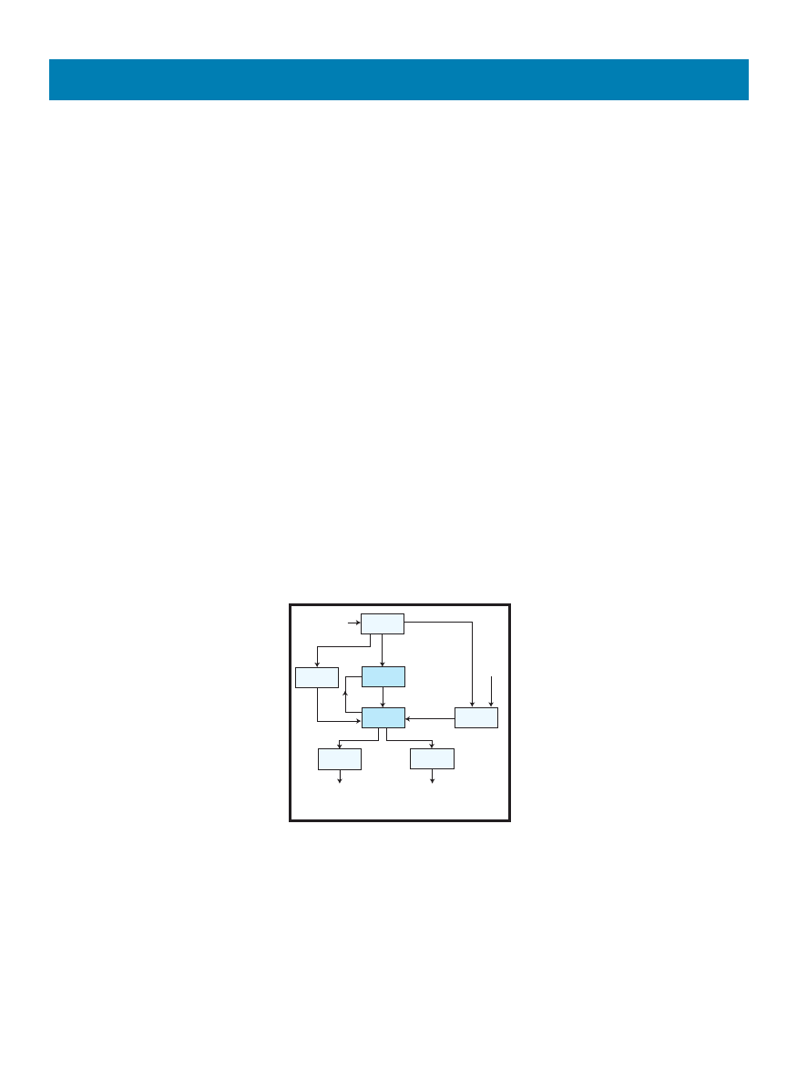
HIGH-LEVEL DESIGN
The simulator was written in Java.
Refer to Figure 1 to see how we organ-
ized the code. Each box represents a
class, and the arrows denote the inter-
action of one class with another. The
outputs of one type of class that are
passed to another class as inputs are
shown on each arrow (e.g., the parser
passes an array of logic elements to
the logic class). For simplicity, only
the major classes and the main
14
Issue 160 November 2003
CIRCUIT CELLAR
®
www.circuitcellar.com
T
oday, one of the most efficient and
cost-effective methods of placing ran-
dom logic in electronic equipment is
to use a microcontroller. Because of
their high I/O capabilities, low cost,
low power, and off-the-shelf availabili-
ty, microcontrollers are widely used in
embedded design projects, from engine
control systems to cellular phones, cal-
culators, and digital clocks. In many of
these real-time applications, a micro-
controller is used to interface to the
external world in order to monitor,
generate, or sample analog and digital
signals by interacting with other hard-
ware. In cases where the design con-
tains both analog and digital signals, it
is usually insufficient to simulate the
digital and analog parts separately.
In an attempt to provide a solution
to this problem, as well as to facilitate
the lab preparation process for the
microcontroller-based digital design
class at Cornell University, we
designed a mixed-signal simulator that
can be used to analyze the analog, dig-
ital (gate level), and program behavior
of small systems built around Atmel
AT90S8515 microcontrollers. The
simulator allows you to set up mixed-
signal systems by using a simple hard-
ware-description language whose syn-
tax is similar to Spice netlist format.
You can also specify the programs to
run on the microcontrollers.
In order to run the simulator, you
must provide a netlist file that lists all
of the electrical connections in the
system, an optional stimulus file
Mixed-Signal AVR Simulator
Engin and Bruce have designed a mixed-signal AVR simulator that you can use to analyze
the analog, digital, and program behavior of small systems built around AT90S8515 micro-
controllers. The simulator is a great tool to have in the classroom, but, as you’ll soon see, it’s
also perfect for your workbench, particularly because you can modify the source code to
handle multiple processors.
describing external events (e.g., button
pushes, received signals, noise, etc.),
and a hex file describing the initial
state of the instruction and data mem-
ories of the microcontroller. (These
hex files can be easily generated from
assembly files using Atmel’s AVR
Studio or a compiler.) After the files
have been provided, the simulator
compiles the circuit, checks for poten-
tial problems, and reports any errors.
After a circuit has been compiled suc-
cessfully, you can run the hex files and
FEATURE ARTICLE
by Engin Ipek & Bruce Land
Parser
Netlist file
Hex file address
Logic element
Logic
Logic
Compiler
Solver
Element A, z
Logic
Hex
reader
Hex file
AT90S8515
XLS
VCD
Analog results
Digital results
Excel file containing
results of analog
simulation
VDC file containing
results of digital
simulation
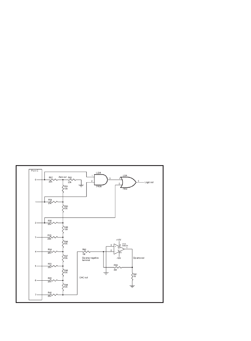
Figure 1—The parser class reads the netlist file. The
compiler class generates linear models of every analog
circuit element for the next iteration. The logic class
instantiates a logic solver based on the information about
the logic gates. The hex reader reads the contents of the
hex file and loads the microcontroller model with the
appropriate data and instructions. The solver class calcu-
lates the voltages at every node for the current iteration.
The current voltage levels at each node are passed back
to the compiler class, which generates linear models of
all circuit elements for the next iteration. The XLS class
creates an Excel file containing the results of the analog
simulation, and the VCD class generates a VCD file
containing the results of the digital simulation.
www.circuitcellar.com
CIRCUIT CELLAR
®
Issue 160 November 2003
15
specified simulation termination time
is reached. At that point, the solver
passes the values it has stored
throughout the simulation to the XLS
and VCD classes, which generate an
Excel file containing the analog
results and a VCD file (to be viewed
by GTKwave) containing the RTL-
level and digital results, respectively.
The nonlinear equations are solved
using the Newton-Raphson algorithm,
while the transient analysis is based on
the Backward-Euler integration formula.
At every iteration, the results for the
shared nodes of all three simulations
(RTL, logic, and analog) are converted to
the appropriate signal domain and passed
as an input to the appropriate model (e.g.,
the microcontroller’s digital outputs that
are inputs to analog circuitry are convert-
ed into analog and passed to the analog
compiler class for the next iteration).
Because of the use of the Backward-
Euler formula, only stable circuits can
be successfully simulated. Hence,
undamped sine wave oscillators
should be implemented using the volt-
age sources. The Wien-bridge oscilla-
tor, for instance, will have an artificial
damping constant associated with it.
Thus, the simulation results will not
reflect the physical reality.
NETLIST FILES
Every netlist file begins with a state-
ment in the form of MCU filename.hex.
Note that filename.hex is the hex file
that contains a memory image of the
initial processor state. This statement is
followed by a description of the connec-
tions in the circuit. In order to make
these connections, you must assign a
unique number from one to n to each
node, where n is the number of nodes
in the circuit (excluding GND).
By default, node 0 always corre-
sponds to ground, but aside from this
convention, you are free to select any
number to correspond to any node.
Listing the element name, the input
and output nodes, and the parameters
related to the operation of the element
specifies connections. For instance,
R 1 2 1000 places a 1-k
Ω
resistor
between nodes 1 and 2. You may
download a full list of the parameters
that must be specified for every ele-
ment from the Circuit Cellar ftp site.
inputs/outputs of those classes are
shown. You may download the code
from the Circuit Cellar ftp site.
The simulation begins when the pars-
er reads the netlist file and determines
the location of the hex file containing an
image of the memory at time t, which
equals zero. This information is passed
to the hex reader, which reads the hex
file and loads the appropriate data and
instructions into the RTL-level model
of the ’8515. The loaded model is then
given to the solver class as an input.
As the parser goes through the
netlist file, it also creates an array of
the logic elements (logic gates and flip-
flops) that you reference. Every logic
element object in this array includes
the type of the element (e.g., D flip-
flop) and the connections to its fan-in
and fan-out. The array is passed to the
logic class, which instantiates a logic
solver based on the nodes, connections,
and initial inputs in the
LogicElement[]
array. This logic solver is then given to
the solver class as an input.
Finally, the parser creates an array of
analog elements with initial conditions
on nodes at time t = 0, and then passes
the array to the compiler class. The
compiler generates linear models of
every component for the next iteration
of the simulation, and it uses these lin-
ear models with the initial conditions
to generate a matrix equation:
Ax = z
where A is an n × n matrix (for n ana-
log components) and z is a vector of
length n.
After the logic simulator, the RTL-
level model of the microcontroller and
the matrix equation are passed to the
solver. The solver determines the
dependencies between the submitted
nodes and solves the matrices and logic
equations for the next time step. It also
advances the microcontroller’s simula-
tion by one clock cycle. The results
from the current time step are returned
to the compiler, which regenerates the
linear models for the next iteration and
passes A and z back to the solver.
This cycle continues until the user-
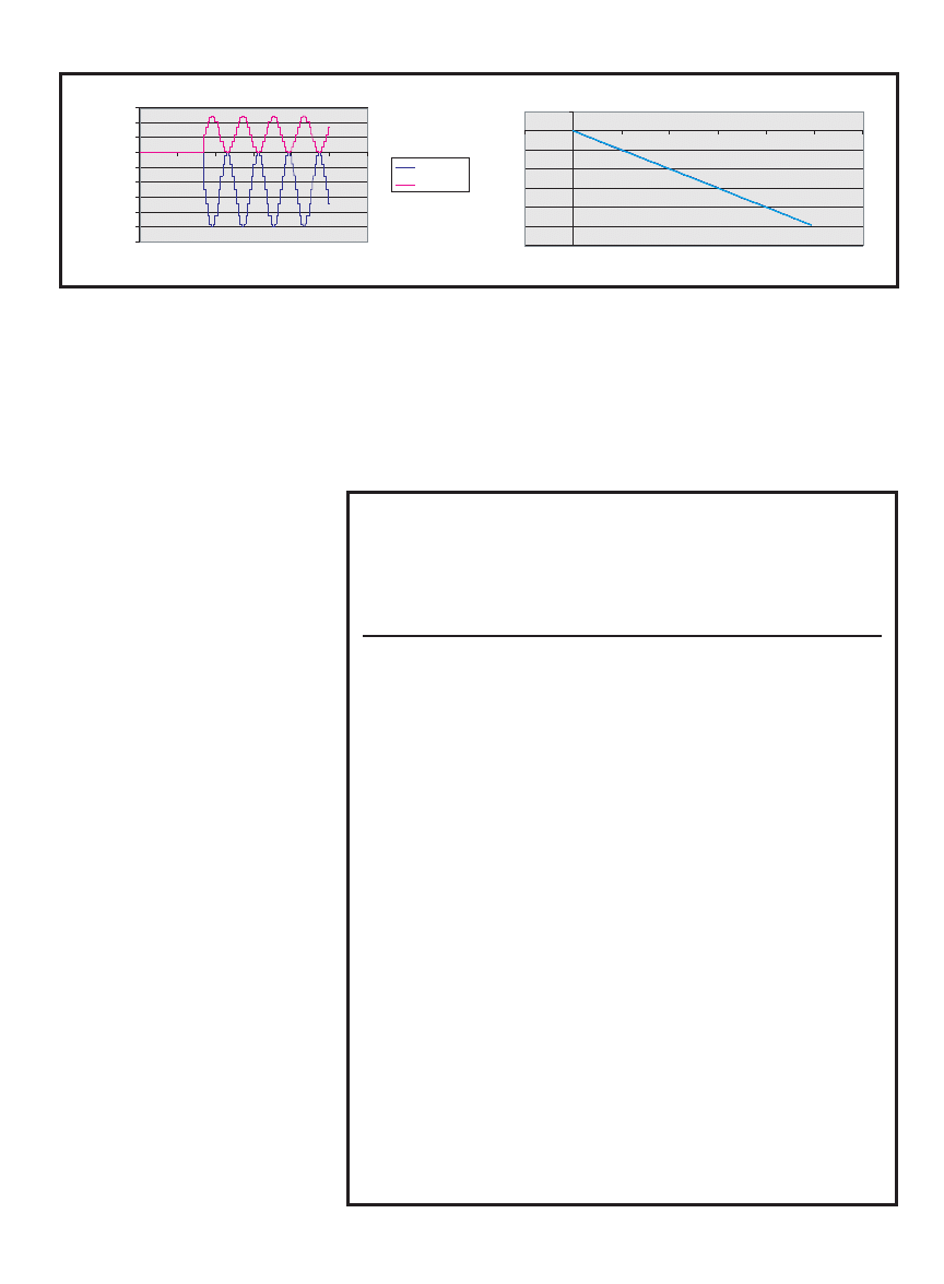
Figure 2—Port C of the microcontroller is set up to generate a sine wave. The output is then converted to analog
using an R-2R ladder DAC. The signal is amplified by an inverting op-amp circuit with a gain of –2. To illustrate
the use of logic gates, the two least significant bits of port C are input to an AND gate, and the result is ORed
with bit 2 of port C.
16
Issue 160 November 2003
CIRCUIT CELLAR
®
www.circuitcellar.com
the node number that you specify.
DUMPLOGIC’s format is identical to
DUMPANALOG’s format.
Buttons and random voltage sources
Connections to the microcontroller
are made by statements in the follow-
ing form:
PORT node_number IO_address
bit_number
where
node_number specifies the num-
ber you assign,
IO_address gives the
address of the port, and
bit_number
shows which bit of the port to connect.
To store the values of any nodes, reg-
isters, or memory locations and view
them after the simulation, use the
DUMP, DUMPANALOG, and DUMPLOGIC
statements. The
DUMP statement is for
the microcontroller, and
DUMPANALOG
is for analog signals. The
DUMPLOGIC
statement is used for logic signals.
The
DUMP statement has the follow-
ing general form:
DUMP name1 memAddr1 name2
memAddr2 … end
where
name1…N is any string you choose,
and
memAddr is the memory address of
the specific register/memory location
that you want to view. The VCD file
uses
name1… nameN when displaying the
results. Because there is no memory
address for the PC, the memAddr field
should be “PC” when storing the PC
(e.g.,
DUMP mcuPC PC end).
The
DUMPANALOG statement has the
following general form:
DUMPANALOG name1 node1 name2
node2 … end
where
name1…N is any string you
choose and
node1…N corresponds to
have stimulus files associated with
them. At each simulation step, the val-
ues for the buttons and random voltage
sources are read from these files. An
Listing 1—The netlist file describes the hardware depicted in Figure 2. The first line specifies the name of
the hex file containing the memory image at t = 0. Statements of the form
R node1 node2
resistance (Ohms) define the DAC. Port C connections are made by statements in the following
form:
PORT bit_number IO_address node_number. The op-amp is defined by declaring
the following:
OPAMP pos_terminal neg_terminal output_terminal pos_sup-
ply_voltage(V). The AND gate is specified by AND input1 input2 output. The OR gate
is similar to the AND gate in terms of its declaration.
DUMP statements map memory locations and nodes
to user specified names so that the results are more readable.
MCU itestsinewave.hex
R 1 9 20000
R 9 0 20000
R 2 10 20000
R 3 11 20000
R 4 12 20000
R 5 13 20000
R 6 14 20000
R 7 15 20000
R 8 16 20000
R 9 10 10000
R 10 11 10000
R 11 12 10000
R 12 13 10000
R 13 14 10000
R 14 15 10000
R 15 16 10000
PORT 1 21 0
PORT 2 21 1
PORT 3 21 2
PORT 4 21 3
PORT 5 21 4
PORT 6 21 5
PORT 7 21 6
PORT 8 21 7
OPAMP 17 0 18
R 17 18 2000000
R 18 0 1000
R 16 17 1000000
AND 1 2 20
OR 3 20 21
DUMPLOGIC logicOUT 21 ENDDUMP
DUMP portc 53 R0 0 R1 1 R2 2 R3 3 R4 5 R5 5 R6 6 R7 7 R8 8 R9 9
ENDDUMP
DUMPANALOG opAmpOut 18 dacOut 16 zeroOut 9 opAmpNegTerminal 17
ENDDUMP
end
Op-amp output vs. DAC output
y = –2x + 2E–11
R
2
= 1
–12
–10
–8
–6
–4
–2
0
2
-1
0
1
2
3
4
5
6
DAC Output (V)
O
p-am
p out
put
(
V
)
Op-amp output vs. number of cycles
–12
–10
–8
–6
–4
–2
0
2
4
6
0
2000
4000
6000
8000
10000
12000
Time (CPU clock cycles)
V
o
lt
ag
e (
V
)
opAmpOut
dacOut
a)
b)
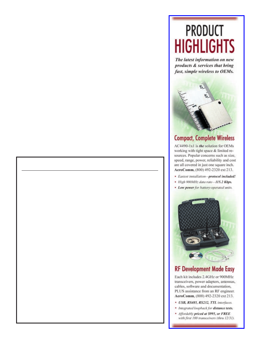
Figure 3a—The voltages at the output of the DAC and the op-amp are shown by dacOut and opAmpOut, respectively. The microcontroller spends the initial 3600 cycles run-
ning the boot code and no changes to port C take place. After the boot code is executed, the microcontroller generates a 4.95-kHz sine wave. The DAC converts the sine
wave to analog and the op-amp amplifies the output of the DAC by a factor of –2. b—The x- and y-axes show the voltages at the outputs of the DAC and the op-amp, respec-
tively. The op-amp’s gain is equal to –2, and the amplifier is perfectly linear because it is an ideal op-amp.


www.circuitcellar.com
CIRCUIT CELLAR
®
Issue 160 November 2003
19
troller was found to be cycle-accurate
in all test cases. The circuit in Figure 2
and corresponding results in Figure 3
are typical outcomes of the simulation.
The circuit in Figure 2 generates a
4.95-kHz sine wave. Port C of the
microcontroller is set up to generate a
new value every one-sixteenth of a
cycle so that you can obtain a total of
16 samples per cycle of the sine wave.
The output is then converted to analog
using an R-2R ladder DAC, and the sig-
nal is amplified by an inverting op-amp
circuit of gain –2. To illustrate the use
of logic gates, port C’s two least signifi-
cant bits are input to an AND gate.
The result is ORed with bit 2 of port C.
Listing 1 is the netlist file describing
the hardware in the schematic diagram.
The first line provides the name of the
hex file to be loaded into the memory.
The DAC is defined next, followed by
the connections to port C and the
logic gates. The
DUMP statements at
the end specify the nodes whose values
example stimulus file is provided below,
assuming that button b1 and random
voltage source v1 have been declared and
tied to this stimulus file in the netlist:
#0
b1 0
v1 0
#5
b1 1
#10
b1 0
v1 2.45
end
The button is off and the random voltage
source is outputting 0 V at cycle 0 (of the
MCU). At cycle 5, b1 turns on. At cycle
10, b1 turns off and v1 outputs 2.45 V.
RESULTS
The results of the simulation were
found accurate to six decimal places
when PSpice analog simulator was
taken as a reference. The microcon-
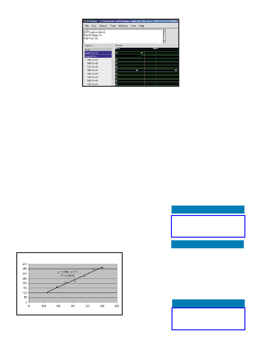
Listing 2—As you study the C code for the sine wave generator, remember that the values for the sine func-
tion are stored in an array. A timer-based interrupt is used to output the next sine value each time it is triggered.
//Sine wave generator using C
//4.95kHz frequency
#include <90s8515.h>
//Define constants
#define prescale1 1
#define clear_on_match 8
//Sample number
unsigned char sample ;
//Table of sine values
flash unsigned char sinetable[16]={0x80, 0xb1, 0xda, 0xf6, 0xff,
0x26, 0x0a,0x00, 0x0a, 0x26,
0x4f};
//***************************************************************
//timer 1 compare-match A ISR
interrupt [TIM1_COMPA] void cmpA_overflow(void)
{
PORTC = sinetable[sample++] ;
//PORTC = Next sine value
if (sample == 16) sample=0 ;
//Go back to beginning of
//table if period complete
}
//***************************************************************
void main(void)
{
sample = 0 ; //Initialize sample # to beginning of table
TIMSK = 0x40 ;
//Timer 1 CompareA
DDRC = 0xff ;
//Port C are outputs
OCR1A = 100; //Set up OCR1A
TCCR1B = prescale1 + clear_on_match ;
//Setup clear on match
TCNT1 = 0;
//Turn on all interrupts
#asm
sei
#endasm
while(1){}
//Do nothing, wait for ISR to be called
}
20
Issue 160 November 2003
CIRCUIT CELLAR
®
www.circuitcellar.com
could be extended to handle
multiple processors by modify-
ing the source code. You could
implement frequency domain
analysis. Furthermore, it
would be relatively easy to
write additional library models
(e.g., an LCD). As a result, we
believe that the simulator
could be used as a teaching tool
in any lab setting.
I
RESOURCES
V. Litovski and M. Zwolinski, VLSI
Circuit Simulation and
Optimization,
Chapman and Hall,
London, England, 1997.
W. H. Press, et al., Numerical
Recipes in C: The Art of Scientific
Computing,
Cambridge University
Press, Cambridge, England, 1993.
PROJECT FILES
SOURCES
AT90S8515 Microcontroller
Atmel Corp.
(408) 441-0311
www.atmel.com
are to be stored in Excel and
VCD files for viewing after the
simulation. These nodes are
also named in the body of the
DUMP statements to facilitate the
viewing process.
Listing 2 shows the C code that
runs on the microcontroller. To
run the simulator, we compiled
this file using the CodeVisionAVR
C compiler with Intel hex select-
ed as the output file format.
Figure 3 depicts the results of
the simulation. The plots are
taken directly from the Excel
file generated by the simulator.
The node names agree with the
definitions in the
DUMP state-
ments. Figure 3a shows the output of
the DAC and the output of the op-amp
versus time. The microcontroller
spends the initial 3600 cycles running
the boot code. Consequently, port C
does not change during this time.
Figure 3b shows the op-amp’s gain. As
expected, the gain is equal to –2, and
the amplifier is perfectly linear because
it is an ideal op-amp. (R
2
= 1 and y = –2x
on the plot.)
The results of the digital simulation
are shown in Photo 1. The top two
rows show the values of port C and the
output of the OR gate, respectively.
The performance of the simulator
was evaluated based on the ratio of the
simulation time to real time. Although
the nonlinear transient analysis algo-
rithm used in the simulator has O(n
3
)
asymptotic complexity, linear circuits
such as the one shown here can be
simulated reasonably quickly. The
program spends a significant amount
of its time (30% for this example) gen-
erating the output files, so reducing
the number of output nodes for which
the simulator saves data significantly
improves performance. Hence, for fast
simulations, only essential signals
should be stored.
Figure 4 depicts the performance of
the simulator for the sine wave gener-
ator example. As indicated by the plot,
the simulator is approximately 700 times
slower with respect to real time, which
is adequate for testing typical micro-
controller-based designs. For instance,
it takes roughly 1.5 min. to simulate
one million instructions of the sine
wave generator, where 10,000 instruc-
tions are enough to see four full cycles
of the sine wave.
THINKING AHEAD
Test results showed that our pro-
gram could successfully simulate the
mixed-signal behavior of small sys-
tems built around
AT90S8515 micro-
controllers in a rea-
sonable amount of
time. The major dif-
ference between our
simulator and simi-
lar commercially
available simulators
is that we provide an
open-source imple-
mentation. Although
only a single micro-
controller is support-
ed, the simulator
was designed so it
Engin Ipek is currently studying
toward a Ph.D. in Electrical and
Computer Engineering at Cornell
University, where he earned his
B.S. His technical interests
include computer architecture,
digital VLSI design, and embedded
systems. You may contact Engin at
ei23@cornell.edu.
Bruce Land is a senior research asso-
ciate in both Neurobiology and
Behavior and Electrical and Computer
Engineering at Cornell University. He
teaches two courses in Neurobiology
and Behavior and one in Electrical
and Computer Engineering. Bruce also
provides general research support in
electronics design and computer tech-
niques. When time allows, he enjoys
neural modeling. You may reach him
at brl4@cornell.edu.
Figure 4—The y–axis indicates the simulation time in microseconds, and the
x–axis indicates the real time in milliseconds. For the sine wave example, the
simulator is approximately 700 times slower with respect to real time.
Photo 1—The top row shows the value of port C at each time step. The
second row corresponds to the output of the OR gate. R0 through R9
show the values of registers zero through nine. As expected, port C output
corresponds to the sine value stored in memory, and the output of the OR
gate corresponds to Port C.0 and Port C.1, or Port C.3.
Simulation time vs. real time
Simulation time (µs)
Real time (ms)

The Motorola Flash Innovation 2003 Design Contest was a great success.
Innovative designs are what we asked for, and innovative designs are what we got—tons of them.
Last spring, engineers began entering projects featuring the HC08 Q-Family from Motorola, and when
our judges sat down to study the submissions, they were presented with entries from such diverse loca-
tions as the United States, Italy, and Thailand. Richard Dreher took the Grand Prize for his Remote
Observation Station, which is an 68HC908QY4-based design that allows you to monitor a track of land
by sending video images to an off-location television. Dozens of other contestants earned First Prize and
Distinctive Entry honors for their innovative, cost-effective designs. Congratulations to the winners!
We would like to thank all of the entrants for helping to make this design contest one of our most
competitive to date. You proved that with a little ingenuity and a straightforward design plan, the poten-
tial for HC08-based embedded applications is limitless.
For complete projects, visit www.circuitcellar.com/fi2003
Flash Innovation 2003 Design
Contest Winners Announcement
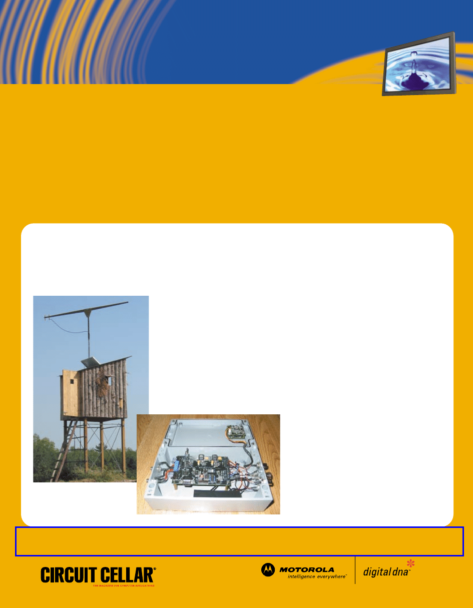
Remote Observation Station
Have you ever wondered what the birds, deer, or bears were
doing in your backyard when you weren’t around? With the Remote
Observation Station, you can watch wildlife on your TV in the com-
fort of your living room. The station includes a camera and transmitter that sends a picture to a TV, which can be up to a mile
or two away. The station gets its power from a PV solar panel and a rechargeable battery, which rely on the system’s control
board for direction. The control board also produces battery state information, which it overlays on the picture sent to your TV.
So, while you’re watching the wildlife, you can also monitor the status of your battery.
The unit integrates six electronic devices, including a CCD video camera, PV solar
panel, rechargeable battery, temperature sensor, RF video transmitter, and the system
control board (PVCC). The control board is based on the Motorola 68HC908QY4 micro-
controller. The board sits at the center of the system, providing a PV charge controller,
two high-efficiency voltage regulators, a video sync separator, and an RS-232 serial
interface for system configuration.
The PVCC control board provides a simple on/off battery charger using the PV solar
panel as a power source. The primary job of the charge controller is to prevent the bat-
tery from being overcharged. The control board also adds battery state information in the
form of a text overlay (on-screen display, or OSD) to the video signal generated by the
CCD camera before it reaches the video transmitter. Additionally, a PC can be connected
to the control board via the DB9 connector.
The system has three operating modes: Configuration mode allows you to control
user settings with your PC; Charge Control mode with OSD sends the battery’s voltage
and temperature to the video signal; and Charge
Control mode without OSD is used when you
don’t need the diagnostic display. The PVCC
configuration utility communicates with the
PVCC board while in Configuration mode. With
this utility, you can set a variety of options,
including the full-charge set point (the off set
point) and the PV reconnect set point (the on
set point). You can also choose to enable the
transmission of an Amateur Radio call sign if a
ham frequency is being used.
Richard Dreher
U.S.
Grand Prize
First Prize
North America and South America Region
For complete projects, visit www.circuitcellar.com/fi2003
NTSC Video Using the 68HC908QY4
The Motorola 68HC908QY4 is used to produce an NTSC video signal that can be
used in several applications. By using a 28.63636-MHz clock, the ‘908QY4 bus
speed is 7.15909 MHz, which is twice the chroma frequency of 3.579545 MHz.
The interrupt timer is used to generate an interrupt every 455 bus cycles, resulting
in an interrupt rate of 15.734 kHz, which is the frequency of NTSC sync. Because
interrupts that occur in the middle of a multicycle instruction are not recognized
until the instruction is completed, the main line consists of a table of NOPs. All of
the sync functions are performed during the inter-
rupt, and the interrupt routine is returned to the
start of the NOP table. The ‘908QY4 can be used
to produce NTSC sync for applications such as an
NTSC test-pattern generator that produces simple
test patterns in order to evaluate a TV’s geometric
distortion, high-voltage regulation, and interlace
quality.
Jed Margolin
Smart-E-Touch
The Smart-E-Touch is an intelligent, touch screen-based user interface design. A
Nitron 68HC908QY4 microcontroller controls and monitors a pair of Motorola e-field
sensors. The e-field sensors, in turn, monitor an XY grid on the PCB for the capaci-
tive sensing of the touch screen. After the Nitron has translated a “touch” from the
e-field sensor data, it then outputs an XY coordinate to its RS-232 serial port. A
main system controller—a PC or equivalent controller—then receives this XY coordi-
nate and can act upon it. The touch screen
is built into the circuit board that houses the
controller circuitry. So, the touch screen is
part of the system controller board. The
Smart-E-Touch is a natural replacement for
resistive touch screens and custom-made
user interfaces.
Bruce Pride
U.S.
Wireless,
Solar-Powered,
Acoustic Wave
Soil Moisture
Detection
System
The advantage of
using acoustic
waves to measure
the moisture con-
tent of soil is that
acoustic waves measure the moisture con-
tent in a volume of soil that radiates out-
ward from the acoustic source to the detec-
tor rather than measure the moisture con-
tent at only one point. Each detector is
solar-powered and uses wireless trans-
ceivers to send the measured data to a serv-
er. The heart of each source and detector
unit (SDU) is the 68HC908QT4. The SDU’s
acoustic source consists of a piezoelectric
speaker excited by a 5-kHz square wave
generated by the 68HC908QT4. The SDU’s
detector unit consists of an electret micro-
phone whose output is AC coupled to a
high-gain, band-pass filter. The result is then
peak detected before being sampled by the
microcontroller’s ADC. The ’908QT4 is con-
nected to a Manchester CODEC and RF
transceiver for communications with a desk-
top computer.
Cheng-Yang Tan
U.S.
Distinctive Excellence
North America and South America Region
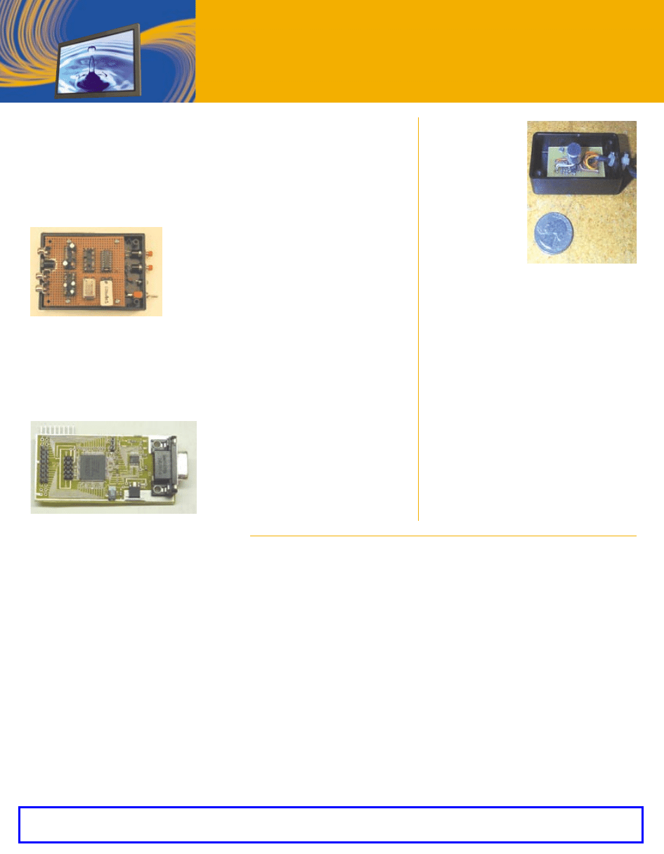
Servo Digitizer
The Servo Digitizer, which is based on the 68HC908QT4, channels control input from a model airplane radio
remote control to a flight simulator program running on a PC. It translates a PWM signal output from the
remote control into ASCII data and sends it to the PC via an RS-232 serial port.
Sitti Amarittapark
, U.S.
Laser Spirograph
The 68HC908QT4-based laser projects onto a primary offset mirror. The primary mirror spins a circular
image onto the secondary mirror, which is also spinning. The secondary mirror then projects the first pattern
onto a wall or screen. The difference in mirror speeds of the two motors creates spirograph-like images.
Matthew Bieker
, U.S.
Printed Circuit Board Drill
The low-cost, fully automated machine drills blank PCBs with minimum custom machining. Data is trans-
ferred to the PCB drill from an Excellon drill file generated by a PCB CAD program running on a PC. The con-
troller is designed around the 68HC908QY4.
Thomas Dvorak
, U.S.
Intelligent Humidity-Compensated Thermostat
Built with an intelligent sensor, 68HC908QY4, and a couple of relays and switches, the thermostat periodi-
cally reads both the temperature and relative humidity of the inside air. Using a preprogrammed table, it com-
pares these temperatures to user-defined preferences, and adjusts the heat or air conditioning accordingly.
Charles Edmondson
, U.S.
Martial Arts Digital Simulator
The interactive martial arts training system incorporates high-quality digitized audio and speech feedback to
simulate sparring with an opponent. The 68HC908QT4 “listens” for impacts on the sensor through its built-
in ADC, monitors the spar time, and tracks the user’s performance during the workout.
Themi Kotsiras
,
Canada
Enviro-Alarm
Built with a 68HC908QT4, an optically isolated remote alarm interface, a low-dropout voltage regulator, a 9-V
battery, and a few sensors, the Enviro-Alarm monitors for leaks around a basement sump pump. The remote
alarm interface connects to a Cat 5 cable that runs to a wiring closet for integration with a PC-based home
automation system.
Kenneth Lumia
, U.S.
Peak Power Controller
The Peak Power Controller acts as an impedance transformer between the source and load. It monitors the
power output from the source and dynamically adjusts the effective load impedance to maintain operation
at the peak power point. The 68HC908QT4-based controller operates as a boost converter, maximizing the
input power.
James McGuire
, U.S.
Flow Rate Failure Detector
The 68HC908QT4-based detector monitors conditions that may cause a rise in temperature, such as a signifi-
cant drop of the air-flow rate and an escalation of the intake temperature. The detector also monitors equip-
ment for overheating.
Colin O’Flynn
, Canada
Nitro-Debugger
The 68HC908QY4-based Nitro-Debugger is a small, non-intrusive debugging device that connects to an exter-
nal circuit board’s microprocessor bus. It monitors, captures, and then converts a single bus cycle into useful
data. The data is displayed by an ASCII terminal emulator via an RS-232 connection.
Bruce Pride
, U.S.
Boost Pump Control
The liquid pump monitor system protects a pump from running dry by monitoring the inlet and outlet pres-
sures. The 68HC908QY2-based system is typically used to assist freon compressors that have long pipes
Innovate with the HCO8
from Motorola
For complete projects, visit www.circuitcellar.com/fi2003
First Prize
Europe, the Middle East, and Africa Region
Low-Cost Intelligent Sensors Network
The low-cost intelligent sensors network is based on
the 68HC908QY4. It is ideal for applications that
require low-speed, two-wire bidirectional data com-
munication, including home or office automation,
remote technological process monitoring, industry
control, security/fire alarm systems, and remote light
control. A simple time-triggered protocol ensures a
predictable data delivery time. The quasi-harmonic
constant frequency network signals are secure from
electromagnetic compatibility problems.
Victor Kremin
Ukraine
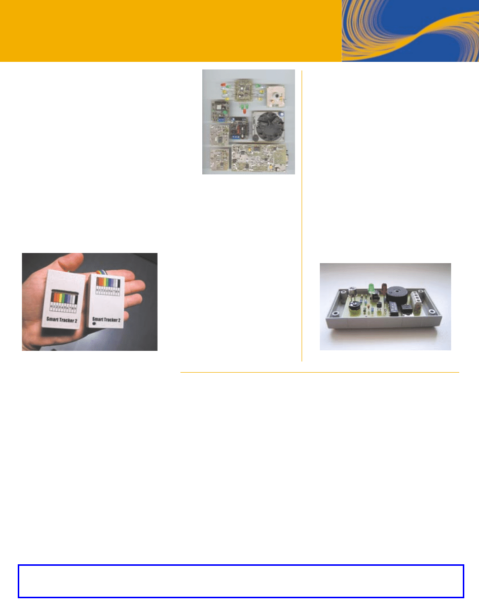
Smart Tracker 2: An Innovative Wire Tracker
The Smart Tracker 2 is a low-cost, compact wire identification device. A 10-chan-
nel transmitter injects test signals into up to 10 wires. A small probe can be con-
nected between any of the wires to identify both of them simultaneously, without a
ground connection. The probe also identifies any short circuits between the wires.
The transmitter has 10 outputs—each identified by a different color—with a small
grabber on each end. The outputs, which are driven by a 68HC908QY4, are con-
nected to one end of the wires to be
identified, in any order. The receiver
has two inputs (red and green) and 10
bicolor red/green LEDs, each of which
is associated with one of the transmit-
ter colors. The transmitter successively
injects a binary word on each of the
10 outputs using a software-based bit-
banging UART transmitter. The receiver
can identify a wire by “listening” to the
input.
Robert Lacoste
France
Gas Alarm
The Gas Alarm is ideal for use in the kitchen
or garage, near a gas boiler, or while camp-
ing. The 68HC908QT2 microcontroller-based
combustible gas detector is small, cost-effec-
tive, and flexible. The electronic circuit evalu-
ates change in the internal sensor resistance.
A few comparators are used to watch the ref-
erence voltage, sensor resistance, and sensor
proper operation. An oscillator isn’t needed
because the detector uses the Nitron micro-
controller’s oscillator. There are built-in delays
for after power-up and after gas is first
detected in order to avoid false alarms. By
changing the sensor type, the detector can be
used for various gases. You can also add an
additional comparator to detect two different
gas concentrations.
Radek Vaclavik
Czech Republic
Magic Lamp
With a 68HC908QT4, some transistors, resistors, and three LEDs (red, green, and blue), the Magic Lamp can
control LED light intensity.
Jens Altenburg
, Germany
Rear Muffler Actuator Control
The Rear Muffler Actuator Control adjusts the sound of an electromotive actuated muffler based on engine
speed. The 68HC908QT4 evaluates the speed, the position of an optional mode switch, and the actuator
current. It also controls the motor driver and provides the control algorithm and safety functions.
Andreas Bartelmus
, Germany
414O Option Board
The Nitron 68HC908QY1CP-based project makes a 4I4O board compatible with a former 4E4S board, and
enables the use of other 0- to 10-V and 4- to 20-mA opto-isolated boards.
Damien Bataille
, France
Artificial Vision System for the Blind
The vision system measures the distance to an object and records the data on a unique hand-held slider,
which is read similarly to Braille. The device estimates an object’s speed using the Doppler effect.
Victor Kremin
, Ukraine
Low-Cost Evaluation Board/Programmer for ’908Qx Series Microcontrollers
The evaluation board enhances the 68HC908Q demo board. This board enables you to build a prototype of a
small device, program 68HC908Q chips, and monitor the connection board using a two-wire (one signal plus
ground) connection to the target system and RS-232C connection to a PC. A 10-position DIP switch is used
to configure the board. There are also three push-button switches and a socket for an oscillator.
Grzegorz Mazur
, Poland
Radio Security System
The Radio Security System system uses a 68HC908QT1-based transmitter and a 68HC908QT2-based receiv-
er to thwart car radio theft by hiding a radio receiver. The theft-deterrent system uses short-distance remote
control with a low-frequency radio signal.
Salvador Perdomo
, Spain
DVD-Thermometer
The 68HC908QT4-based multimedia DVD-Thermometer displays the temperature on a TV with full-color graph-
ics. Animated pictures can be added along with CD-quality audio announcements.
Alberto Ricci Bitti
, Italy
Wireless Mousetrap Monitoring System
The 68HC908QT4-based system consists of a monitoring station—a computer-controlled receiver with an
LCD and a relay output—and up to 20 mouse sensors. A sensor is placed inside each live-catch trap. When a
mouse is captured, the sensor transmits the trap ID to a master unit, which logs the trap ID and displays it
on the LCD. The receiver can also dispatch a call to an external service, triggering an ordinary automatic
phone dialer connected to its relay out.
Alberto Ricci Bitti
, Italy
Counter
The Counter is based on the MC68HC908QTx. Five seven-segment LEDs are used for display. Powered by a
single 5-V power supply, the counter is ideal for industrial process control and monitoring applications.
Tito Smailagich
, Yugoslavia
Tiny Altimeter
The Tiny Altimeter measures altitude and can store data in internal memory every 200 ms. Based on the
68HC908QT4, the altimeter measures atmospheric pressure and recalculates pressure changes to the alti-
tude values without an antenna. The system achieves 0.5-m (1.6
′
) resolution.
Radek Vaclavik
, Czech Republic
Distinctive Excellence
Europe, the Middle East, and Africa Region
First Prize
Asia and the Pacific Rim Region*
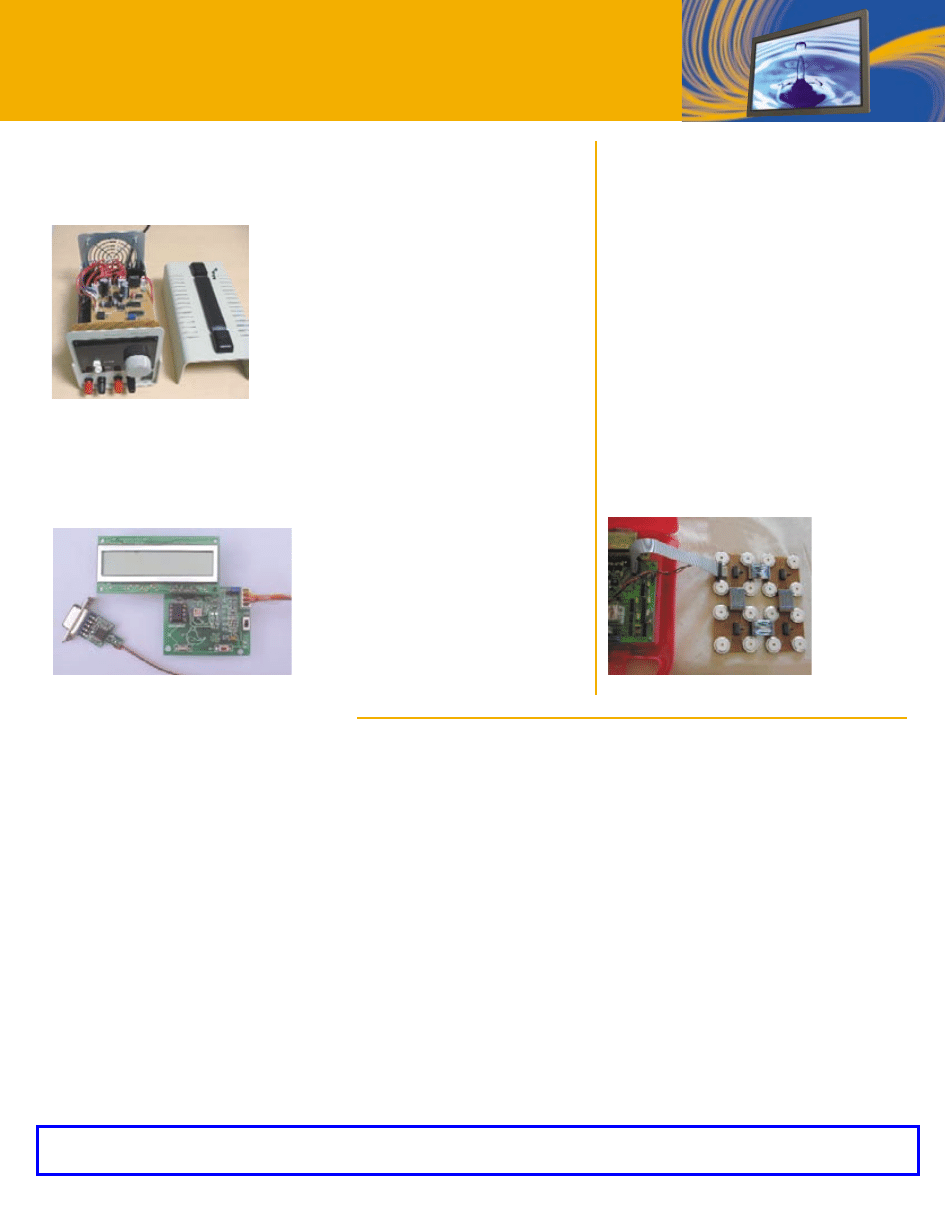
Programmable DC Power Supply
Instead of the classic transformer—with a regulator, lots of wires, and a 5-V
power supply—this power supply is more like a real tool. The power supply is
based on the 68HC908QT4, and features 0.6- to 20-V output voltage with 8-mV
resolution, and 0- to 2.5-A output current with
10-mA resolution. Other features include short-
circuit protection, adjustable current limit (5-ms
response time), 5-mVPP maximum output ripple,
and a 2 × 16 LCD. The power supply can drive
the LCD using only three I/O lines, two of which
are shared with other peripherals. The resolution
of the internal ADC can be increased from 8 to
14 bits. Integer arithmetic is used to save com-
putational power and ROM.
Mihai Tudosie
Japan
Tilt Detector
The Tilt Detector is based on a 68HC908QT4 microcontroller. The small detector
can measure 360° of tilt and display the result on its LCD, which is controlled by
only two pins. The tilt data is stored in the detector and can be displayed on the
screen. The detector can handle operations, or it can send stored data to a PC. In
order to improve the measurement accuracy, the gadget can calibrate the sensor
and save the calibration parameters for
better performance. It can also measure
acceleration in the range of –2 to +2 g.
There are two versions of the circuit: one
is a digital version, which is powered by
an input capture function with high accura-
cy, and the other is a low-cost analog ver-
sion, which is powered by the inner ADC.
Hua Zhou
China
For complete projects, visit www.circuitcellar.com/fi2003
µTelemetry: The Micro Telemetry System for R/C Race Cars
The µTelemetry is an inexpensive, wireless telemetry system that monitors voltage, speed, and temperature
in real-time. It was designed for use in remote-controlled race cars, but also works well for a variety of data-
acquisition applications. The transmitter and receiver are designed with the 68HC908QT4.
Virachat Boondharigaputra
, Thailand
Intelligent Fishbowl
The Intelligent Fishbowl controls and displays the temperature in a fishbowl, and also automatically feeds
the fish. Based on the 16-pin 68HC908QT2, the low-cost system also controls lighting for the fishbowl.
Zhang Chongguang
, China
Mini Node
The Mini Node is a creative solution to the horizontal switch plates now popular in Australia. To continue
using an HCS II and X10 system for home control, the 68HC908QT4-based Mini Node connects to the HCS
II via the RS-485 network. It automates house lights that are controlled by more then one wall switch.
Kamal Gendi
, Australia
iButton-based Personal Identification System (iBPIS)
For use in offices, the iBPIS stores personnel information on the Maxim iButton; the data then can be dis-
played on a PC or hand-held device through an IR link. The system consists of three modules: the
68HC908QT4-based iButton user module (iBU), the iButton enquiry module (iBE), and iButton programming
module (iBP).
Sunil Jha
, India
Low-Power Optical Smoke Detector
The 68HC908QT4 is the core processor of the Low-Power Optical Smoke Detector. Using an infrared LED
and receivers, the unit detects the presence of smoke particles in the air, thus triggering a signal to any com-
mercial fire-monitoring panel so that an alarm can sound or other recovery actions can be taken.
Steven Wong Kai Juan
, Singapore
Blood Pressure Monitor
The Blood Pressure Monitor measures the oscillations in pressure in the cuff. A sensor translates the pres-
sure to capacitance, which is then measured by a 68HC908QT4-based circuit. The circuit also detects the
small variations in pressure during deflation to calculate the systolic and diastolic readings, which it displays
on a
1 × 16 LCD.
Ganesh Raaja Maharajan
, India
Automobile Cruise Control
The stand-alone Automobile Cruise Control is a microwave radar-guided, 68HC908QT4-based cruise control
system for all types of vehicles. Using the Doppler effect, the system detects stationary and moving objects
50 to 75 m ahead or behind the vehicle.
Indranil Majumdar
, India
VGA Signal Probe
This VGA Signal Probe uses a 68HC908QT4 to digitize an analog signal and generate a corresponding VGA
video signal that represents the time sequence of the samples. This allows a simple audio-bandwidth CRO to
be implemented using two eight-pin ICs.
Lindsay Meek
, Australia
Intellistick: The Eye of the Blind
The 68HC908QT4-based Intellistick is a walking stick for blind people that uses ultrasonic ranging to detect
obstacles. Audible warning sounds (various beeps) indicate the distance of the obstacle.
H.N. Naveen
, India
RS-232-to-RS-485 Communications Multiplexer
The multiplexer provides eight RS-485 communications ports using one RS-232-to-RS-485 conversion circuit.
A 68HC908QY1 controls eight analog switches and builds connections between a real RS-485 communica-
tions port and any one of the eight virtual ports. You can control the target channel manually, let the MCU do
it automatically, or use a specially designed program running on the PC. An LCD displays the statuses.
Hua Zhou
, China
Distinctive Excellence
Asia and the Pacific Rim Region*
Acoustical Cellular Automata
Parallel Processor
The mathematical concept known as cellular
automata (CA) is primarily modeled as a two-
dimensional graphical presentation. Humans
have the ability to localize sound sources in
two and even three dimensions due to the
physical shape of the human head and ears.
Thus, we have the ability to discern the posi-
tion of the sounds around us. The Acoustical
Cellular Automata Parallel Processor applies
cellular automata to a two-dimensional array
of sound emitters. The design uses multiple
microcomputers connected in a two-dimen-
sional array to form a larger parallel array
processor. The array processor, built with the
68HC908QY4, is programmed to handle the
specific case of CA with multiple sound emit-
ters to display the cell states. The microcom-
puter module actually controls four cells in
the array, and is connected to four sound
emitters (transducers). The module can be
connected
to other
modules to
form a large
array that
could con-
ceivably
cover a
wall.
Raymond
Weisling
*Includes all other countries not included in other regions

28
Issue 160 November 2003
CIRCUIT CELLAR
®
www.circuitcellar.com
A
s a hardware designer and manag-
er, I’ve noticed that many electrical
engineering students are often missing
something when they begin their first
full-time jobs. They’ve been taught
how to design great circuits, some of
them quite complex, but they haven’t
been taught the importance of timing.
What does timing analysis mean?
Why is timing analysis important?
How is it done? In this article, I
answer these questions. In addition, I
present you with a real design prob-
lem that was solved with timing
analysis. So, here we go!
WHY TIMING ANALYSIS?
There are a couple of reasons for
performing timing analysis. First and
foremost, it can be used to verify that
a circuit will meet all of its timing
requirements. Timing analysis can
also help with component selection.
An example is when you are trying to
determine what memory device speed
you should use with a microprocessor.
Using a memory device that is
too slow may not work in the
circuit (or would degrade per-
formance by introducing wait
states), and using one that is
too fast will likely cost more
than it needs to.
A WORKING DEFINITION
Timing analysis is the
methodical analysis of a digital
circuit to determine if the tim-
and hold timing. Red indicates that a
condition has not been met. If the set-
up time is read and has a margin of –1,
the set-up time has not been met and
is off by 1 ns. The hold time indicates
that there is 1-ns margin.
In Photo 1, the gray areas of the
waveforms indicate the uncertainty of
when the edge occurs. Notice that the
output of logic gate 2 has the largest
uncertainty, because the uncertainty
is cumulative as you go through a
delay chain. So, the delay at the out-
put of logic gate 2 is equal to the delay
from CLK A to Q of flip-flop A as well
as the delays through logic gates 1 and
2. Note that the waveform also uses
color highlighting to indicate that con-
straints are not being met.
As you can see in Photo 1, there is a
D input set-up time problem to flip-
flop B. Sometimes, when discussing
timing issues, I hear designers say that
timing doesn’t really matter because
the processor has a memory controller
with variable timing. This may be true,
but it usually means that the
processor allows for a pro-
grammable number of wait
states. If you add another wait
state (i.e., one more clock
cycle before clocking in the
data), then the problem in
Photo 1 will go away. But
what if you don’t want the per-
formance hit of adding a wait
state, or what if the processor
doesn’t allow wait states? You
Timing (Analysis) is Everything
FEATURE ARTICLE
by Philip Nowe
Philip’s main issue with young engineers is that many of them have been taught excellent
circuit design techniques but haven’t been schooled in the importance of timing analysis.
What is timing analysis? Why is timing analysis important? How do you perform timing
analysis? Whatever your level of expertise, you’re sure to find Philip’s answers informative.
ing constraints imposed by compo-
nents or interfaces are met. Typically,
this means that you are trying to
prove that all set-up, hold, and pulse-
width times are being met.
A minimum or maximum digital
simulation is not actually the worst-
case analysis. That is what a number
of entry-level engineers believe. The
worst-case analysis takes into account
minimum delays through some paths
and maximum delays through other
paths. For instance, the worst-case
set-up timing with respect to flip-flop B
in Figure 1 would be the minimum
delay to the clock input combined
with the maximum delay to the data
input of flip-flop B.
Let’s assume the timing values in
Table 1 are for the circuit elements in
Figure 1. Do you think that there is a
problem with these values? Take a
look at this circuit in a waveform
view in Photo 1. Notice that the bot-
tom of the photo shows the parame-
ters used in determining the set-up
D
Q
D Flip-flop
A
CLK
CLK A
Logic
gates
1
Logic
gates
2
D
Q
D Flip-flop
B
CLK
Clock
delay
CLK B
Figure 1—The simplified digital circuit contains delays in the data and the
clock paths. The timing values are shown in Table 1 (see p. 29).
A How-To Guide for Timing Analysis
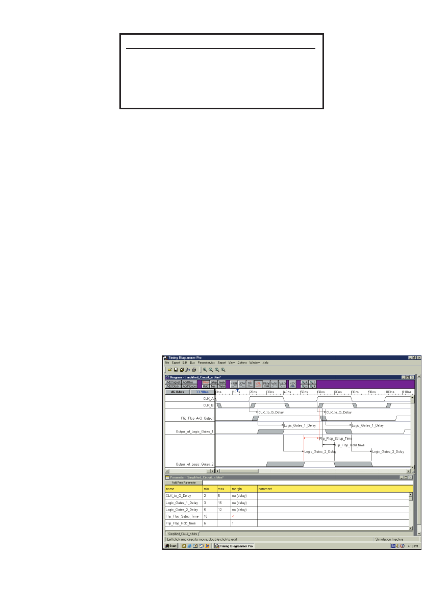
www.circuitcellar.com
CIRCUIT CELLAR
®
Issue 160 November 2003
29
the signal timing, I put on
the diagram the minimum
and maximum timing for
every signal edge. Each
time I changed the compo-
nents in a signal path, I
updated the numbers on
the drawing. The next pos-
sible step in the evolution
of timing analysis would
be to put the timing num-
bers in a spreadsheet and let the
spreadsheet do the calculations.
Table 2 shows the original simpli-
fied circuit analyzed in a spreadsheet
format. For the set-up time calcula-
tion, use the maximum data delay and
the minimum clock delay (less set-up
time) to determine if the set-up time
is met. For the hold time, use the
minimum data hold delay and the
maximum clock delay plus the hold
time to see if the hold time is met.
This is straightforward but time-con-
suming. What you need to do is to cal-
culate each of the signal paths going
to flip-flop B, for instance. The advan-
tage of using a spreadsheet is that it
saves you time when making changes
to the design. A combination of a
spreadsheet and a drawing seems like
the right way to go.
I’m familiar with two popular semi-
manual timing analysis products:
would have to solve the
timing problem.
Another case involves
hold problems. Adding
wait states often cannot
solve this, because the
timing chain for the
D input is tied to the
current clock edge not to
the delays from the pre-
vious clock edge. In such
a case, you need to make some
changes to the design to make the
timing work.
Okay, so you agree that there is a
problem. So what? What will happen
if you don’t fix it? There are three
possibilities for set-up and hold times
(see Figure 2).
As you can see in Figure 2a, the sig-
nal of interest can meet the timing
with proper set-up and hold times.
The next possibility is that the signal
may miss it completely and get
caught on the next clock edge (see
Figure 2b). (Note that this can be a
problem if you don’t want the per-
formance penalty.)
The last possibility is that the input
signal changes inside of the set-up and
hold window (see Figure 2c). What
happens in this case? The output of
the flip-flop can become metastable,
which means that the output can
oscillate from zero to one or from one
to zero a few times (or many times)
before it stabilizes to a zero or one.
The resulting state is random. (For
more information on metastability,
refer to H. Johnson and M. Graham’s
book, High-Speed Digital Design: A
Handbook of Black Magic
).
Obviously, this is not a good situa-
tion, because the output of the flip-
flop may be wrong, and it may take
longer than the normal propagation
delay to get to the wrong value.
Knowing that you have a problem is
the first step. So, how can you fix it?
There are many ways to solve timing
problems. In this simplified circuit, you
are off by 1 ns. You can change either
logic gates 1 or 2 so that they are faster
parts. Another option is to select a flip-
flop that has a smaller set-up and hold
window. Timing analysis doesn’t fix
the problem; it just tells you that there
is a problem. Remember, when you
make a change to your circuit, rerun
the timing analysis to make sure that
the problem is fixed and that another
one hasn’t been created. Hopefully, I
have convinced you that timing analy-
sis is important. Now I’ll show you
how to do it.
HOW IS IT DONE?
Timing analysis has been achieved
in many different ways over the years.
You can use anything from a manual
approach (i.e., using spreadsheets and
a drawing program or just pen and
paper) to what I refer to as semimanu-
al CAD programs. You can also use
fully automatic static and dynamic
timing-analysis tools.
I am visually oriented like most
engineers, so I prefer to draw my timing
diagrams. For the first board I devel-
oped, I used my schematic drawing
tool to draw the timing waveforms. For
Table 1—Here are the timing values for the circuit illustrated in Figure 1.
Photo 1—I used Timing Diagrammer Pro for the timing analysis of the simplified digital circuit. Note that the gray
areas on the waveform denote regions of uncertainty. The red areas show a timing violation.
Timing parameter
Minimum value
Maximum value
Nominal CLK frequency
25 MHz
25 MHz
CLK to Q delay (both flip-flops)
2 ns
5 ns
Clock delay
1 ns
3 ns
Propagation delay through logic gates 1
3 ns
15 ns
Propagation delay through logic gates 2
5 ns
12 ns
D input setup time to CLK (both flip-flops)
10 ns
D input hold time after CLK (both flip-flops)
6 ns
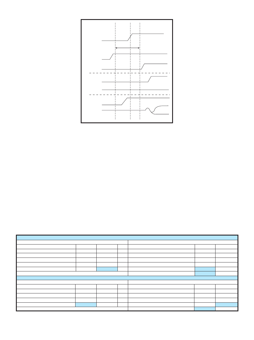
30
Issue 160 November 2003
CIRCUIT CELLAR
®
www.circuitcellar.com
SynaptiCAD’s Timing
Diagrammer Pro and Forte
Design’s Systems
TimingDesigner. These two prod-
ucts are roughly similar. The
timing diagrams in this article
use Timing Diagrammer Pro.
The Timing Diagrammer Pro
is a timing analysis tool
designed to assist the digital
designer in modeling and ana-
lyzing digital circuits. (Another
tool from SynaptiCAD is
Waveformer Pro, which also
allows you to export waveforms
as VHDL or Verilog for simula-
tion purposes.) It has two main
windows for analysis, the first
of which is the diagram editor
window where you draw the
waveforms. There are special
tools to help with clocks, and
you can create waveforms from
other waveforms. You can do
so with a Boolean equation—
(SIG0 and SIG1 and SIG3) delay
20 ns—or it can be specified using
VHDL or Verilog. The other impor-
tant window is the parameter win-
dow, which is like the aforemen-
tioned spreadsheet; it holds the tim-
ing parameters of the design. The
power of Timing Diagrammer Pro is
that the parameter values and the
timing waveforms are linked.
TIMING DIAGRAMMER PRO
Performing a timing analysis using
Timing Diagrammer Pro is straight-
forward. First, you need to draw in
the waveforms. Initially, there are no
delays or constraints; you don’t have
to be accurate at first, because the
accuracy comes when you add the
delays and constraints.
Second, you need to add the delay
and constraint information to the
waveforms; this will automatically
add the delays and constraints to the
parameter spreadsheet. Then, enter
the exact minimum and maximum
numbers for the delays and con-
straints in the parameter spreadsheet.
Doing so automatically updates the
view in the diagram editor win-
dow and shows the areas of tim-
ing uncertainty.
Timing Diagrammer Pro
allows you to use libraries of
timing values for parts. Thus,
you can reuse some of the work
that you’ve (or someone else)
done already.
DESIGN SEQUENCE
You now know how to use
Timing Diagrammer Pro to per-
form timing analysis, but how
can you use the tool in a real
project? The following sequence
has worked well for my team for
a number of design projects.
First, capture the interface
specifications in Timing
Diagrammer Pro with all of the
timing constraints shown. An
interface is any part of the design
that interacts with another part,
such as a write cycle from a
microprocessor to a memory and
a connection to a PCI bus. These inter-
face specifications form the basis for
subsequent design decisions; they may
give the designers an early indication
as to whether the design is feasible,
impossible, or sheer lunacy. For
instance, if the interface specifications
dictate that you will have to use a
34-ps SRAM, you’ll probably try to get
on another design project!
As the design progresses, put real tim-
ing numbers into Timing Diagrammer
Pro, which will immediately tell you
if the constraints are still met. At
CLK
T
SU
T
H
State
unknown
D
Q
D
Q
D
Q
Figure 2a—Data arrives before the set-up time requirement. Data is
clocked into the flip-flop on the rising edge of CLK. b—Data arrives after
the hold time, which results in the data being clocked into the flip-flop on
the next rising edge of CLK. c—Data arrives within the set-up and hold
window, which results in an indeterminate output from the flip-flop.
a)
b)
c)
Table 2—For the simplified circuit, the set-up time slack is equal to the minimum clock delay minus the maximum data delay. The hold time slack is equal to the minimum data
delay minus the maximum clock delay.
Set-up time calculation
Data delay
Clock delay
Timing parameter
Minimum (ns) Maximum (ns)
Timing parameter
Minimum (ns) Maximum (ns)
CLK A or CLK B to Q delay
2
5
CLK A or B period
40 40
Propagation Delay1 through logic gates
3
15
CLK A to B delay
1
3
Propagation Delay2 through logic gates
5
12
Minus D input setup time to CLK1
10
10
Total data propagation delay
10
32
Time from CLK to CLK1 accounting for set-up time
31
33
Slack for set-up time
–1
Hold time calculation
Data hold
Clock delay
Timing parameter
Minimum (ns) Maximum (ns)
Timing parameter
Minimum (ns) Maximum (ns)
CLK A or CLK B to Q delay
2
5
CLK A to B delay
1
3
Propagation Delay1 through logic gates
3
15
D input hold time after CLK B
6 6
Propagation Delay2 through logic gates
5
12
Total data hold time beyond CLK B
10
32
Time from CLK to CLK1 accounting for set-up time
7 9
Slack for hold time
1
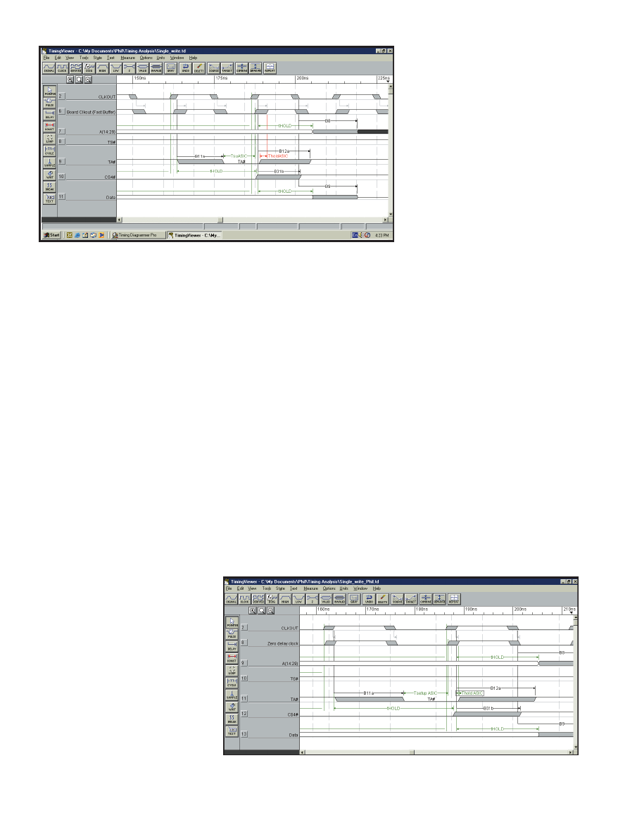
www.circuitcellar.com
CIRCUIT CELLAR
®
Issue 160 November 2003
31
some point, there may be more than
one option. Using this tool, you can
model each of the possible solutions
to determine if they work. If they do
not work, then redesign, whether that
means simply changing to a faster
component or a completely new cir-
cuit. An alternative might be to
change the original requirements,
assuming that your customer allows
you to do so. Don’t count on it!
When it comes time to review your
design prior to building your PCB, for
instance, if the Timing Diagrammer
Pro files are up to date, you have proof
that your design will meet the timing
requirements. Note that if your circuit
has critical timing paths, you may
want to include PCB delays in the
timing analysis as well.
AUTOMATIC CAD TOOLS
ASIC designers have been using stat-
ic timing analysis tools for a long time.
Synopsys’s Primetime is an example.
The tools go through the entire design
and determine if there are any timing
violations (with some constraints from
the user to minimize false paths). There
are static timing analysis tools for
board-level design, as well (e.g., BLAST,
which was developed by Innoveda).
These tools generally cost significantly
more than Timing Diagrammer Pro
and Timing Designer.
What if a tool shows that you are in
error? Is this always true? You may say
that timing analysis is too pessimistic
and, at times, you may be right. For
instance, if the elements in the simpli-
fied circuit depicted in Figure 1 are in
one FPGA, it is less likely that the
data path will exhibit a maximum
delay and the clock path will exhibit a
minimum delay. This is because they
are in the same part, and delays on a
chip tend to track each other. The data
path may be at the maximum delay
but the clock delay will be too. For
most other cases, however, it is best to
use worst-case timing numbers.
A PROBLEM SOLVED
At a former employer of mine, we
had a problem with a card we were
working on. We couldn’t write to some
of the address space in one of our
ASICs on a new spin of the card. So,
after playing with the software to make
sure that it was not the cause of the
problem, we hooked up the logic ana-
lyzer to see what was going on. At first
glance, the timing looked fine, and we
scratched our heads. But just before we
went home late that evening, one of
the ASIC designers said that he found
it funny that the first write cycle that
had worked was the only one that
worked. It would have been nicer if he
had mentioned that earlier!
When we returned to the lab the
next day, we concentrated on looking
at the second and subsequent write
cycles. One of the control signals to
the ASIC was rising at the same time
as the clock. Our hypothesis was that
the timing wasn’t OK.
We decided to try moving the clock
signal in time by delaying the clock.
We initially did this by adding a long
wire to the clock signal. As a result,
the write cycle worked! Well, it most-
ly worked. Next, we used a footprint-
compatible buffer, which was slower
and seemed to work well enough for
the card to be used by the SW develop-
ers and other testers to continue with
their work. However, it didn’t explain
exactly what was wrong. Why was the
control signal so close to the clock sig-
nal? Why hadn’t we seen this on the
previous version of the card?
We went back to the timing analysis
for the previous version of the card, and
it showed that there shouldn’t have been
any problems. On closer inspection,
however, we noticed that the analysis
was done to the wrong clock edge. When
the timing analysis was changed to
the correct clock edge, it immediately
Photo 2—Note the width of the Board Clkout signal. This is the result of it being an ordinary buffer that is heavily
loaded on the board. Again, red indicates a timing violation.
Photo 3—I used a zero-delay clock driver. The area of uncertainty on this clock is significantly less than the Board
Clkout signal in Photo 2. Notice the lack of red this time. It works!
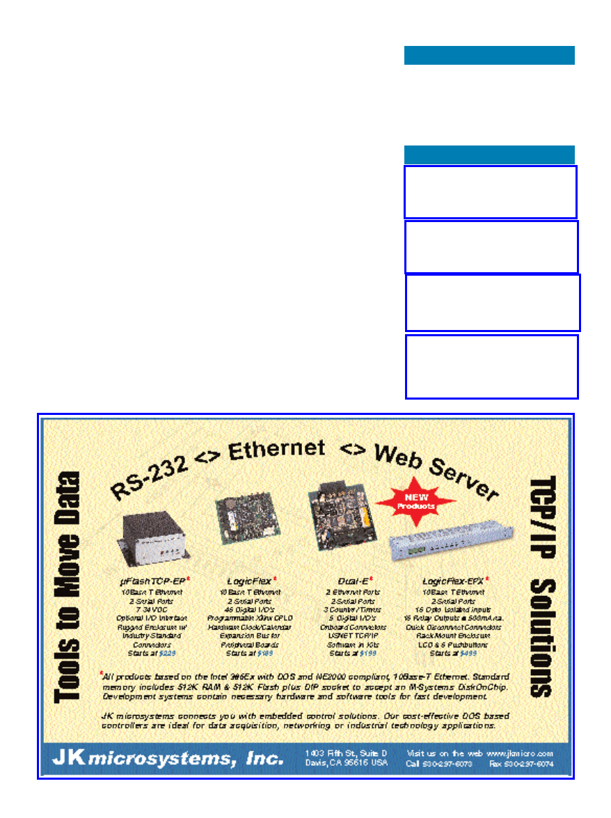
32
Issue 160 November 2003
CIRCUIT CELLAR
®
www.circuitcellar.com
SOURCES
Timing Designer
Forte Design Systems
(800) 585-4120
www.forteds.com
BLAST
Mentor Graphics Corp. (Innoveda)
(800) 547-3000
www.innoveda.com
PrimeTime
Synopsys, Inc.
(800) 541-7737
www.synopsis.com
Timing Diagrammer Pro and
Waveformer Pro
SynaptiCAD, Inc.
(800) 804-7073
www.synapticad.com
RESOURCE
H. Johnson and M. Graham, High-
Speed Digital Design: A Handbook
of Black Magic
, Prentice Hall,
Upper Saddle River, NJ, 1993.
Philip Nowe earned a Bachelor’s in
Engineering at Carleton University in
Ottawa, Canada. He has been work-
ing in the hardware design industry
for the past 20 years. He has experi-
ence in board design, PLD/FPGA
design, and hardware management.
Currently, Philip is a digital design
consultant. You may contact him at
pnowe@sympatico.ca.
flagged that there was a problem.
Why wasn’t there a problem with
the previous version of the card? After
talking to the software folks, we found
out that the same write cycle on the
previous version of the card didn’t
work either! They had found a way
around it, so they didn’t complain too
loudly. At that point, we knew that
we had a problem that needed to be
solved on both circuit cards. The prob-
lem with the timing in the circuit was
that the clock was being delayed quite
a bit because of the load on the clock.
The new version of the card added two
more loads to the clock line, which,
in turn, caused the clock to rise more
slowly and arrive coincidently with
the control signal.
We looked at the buffer and found
another part that was a zero-delay
buffer, which meant it had a PLL in it to
synchronize the output clocks with the
input clock. We put the timing numbers
from the new part in the timing analy-
sis, and it worked. We then dead-bugged
the part on the board, which was not an
easy feat with a number of BGAs. After
we had solved a few other problems
with the ASIC, the board worked.
Photo 2 shows the timing analysis
for the circuit with the old clock
buffer. Photo 3 depicts the timing
analysis with the zero-delay buffer. (I
used Forte Systems’s Timing Viewer,
because the analysis was performed
in Timing Designer.)
CONVINCED YET?
I hope I’ve convinced you of the
importance of timing analysis, which
you can now perform manually or with
a semiautomatic CAD tool. Remember,
whether you have a design running at
1 MHz or 1.5 GHz, timing matters!
I

Open Frame Power Supplies
Jameco offers a wide selection of open-frame
power supplies suitable for production, pro-
totype and design environments. Be sure to
check out our selection of Artesyn, Mean Well
and dozens of other brands with universal input, PFC
and other features you need on our web site today!
Wall Transformers
We offer a complete selection of AC-to-AC
and AC-to-DC wall transformers for general
purpose and production applications.
Most are UL approved and available
with various power plugs.
Be sure to visit our web site
and learn more.
Low-Noise Fans
Jameco offers hundreds of low-noise fans at
outstanding prices. These agency-approved low-profile
fans feature ball or sleeve bearings so you can be
assured your system will be run-
ning cool for years to come.
Get more details by asking
for a FREE catalog today.
Table-Top Transformers
Outfit your product with a professional table-top
transformer. Jameco offers a wide variety
of configurations with regulated and
unregulated outputs. Don’t forget to ask
for a FREE catalog and learn about our
selection of domestic and international
input power cords.
DC-to-DC Converters
Jameco now offers a wide selection of Isolated
and Point-of-Load DC-to-DC converters suit-
able for distributed power architectures.
Avoid the hassles of “large company”
distribution channels and get immediate
delivery from Jameco today!
219150MC
102955MC
184866MC
155213MC
210809MC
Mfr. Cross
Output Rating
Input
Jameco
Mfr.
Reference No.
(Volts@Current)
(VAC@Hz)
Part No.
Price
Mean Well
S-25-5
+5V@0-5A
85-264@47-63
123246MC
$43.95
Mean Well
S-60-24
+24V@0-2.5A
85-264@47-63
123351MC
57.95
Mean Well
S-150-24
+24V@0-6.5A
88-132/176-264@47-63 123449MC
76.95
Mean Well
SP-300-24
+24V@0-12.5A
88-264@47-63
137402MC
185.95
Power-One
PFC-500-1024
+24V@0.6-21A
85-264@47-63
202905MC
69.95
Mfr. Cross
Output Rating
Jameco
Manufacturer
Reference No.
(Voltage@Current)
Part No.
Price
Skynet
SNP-0502-B
+5V@0-2A
184866MC
$13.49
Artesyn
NLP25-7608
+5V@0.2-2A; +12V@0.1-0.8A;
218501MC
39.95
-12V@0-0.1A
Mean Well
PS-65-24
+24V@0-2.7A
148646MC
33.95
Artesyn
NLP150L-96Q5366
+3.3V@0.5+10A;
219029MC
116.85
+5.1V@1.5-2.0A;
+12V@0-2A;+12V@0-0.65A
Digital Power
USS250-115
+15V@0-16.5A
204564MC
49.95
Mfr. Cross
Output Rating
Size (+0%-20%)
Agency
Jameco
Reference No.
(Volts@Current)
H" x W" x D"
Approvals
Part No.
Price
DC1205F12
+12@500mA
2.5 x 1.9 x 1.6
UL/CSA
102496MC
$4.95
SC102TA1200-B02
+12@1500mA
2.9 x 2.0 x 2.6
UL/CUL
210809MC
12.95
DCR1205F12
+12@500mA
3.2 x 2.2 x 1.9
—
162996MC
8.95
DC1205F5
+12@500mA
2.5 x 2.1 x 1.7
UL/CSA
102277MC
4.95
41-2-15
+12@300mA
2.9 x 2.0 x 1.6
UL/CSA
190043MC
4.49
Mfr. Cross
Power
Output Rating
Input
Size (+0%-20%) Jameco
Reference No.
(W)
(Volts@Current)
(VAC@Hz)
H" x W" x D"
Part No.
Price
SPU50-6
60
+24@2.5A
100-240@47-63
5.6 x 2.9 x 1.6 161605MC $44.95
P40A-3P2JU
40
+12@3.3A
100-240@50-60
5.5 x 2.3 x 1.5 155213MC
34.95
SPU50-3
60
+12@5.0A
100-240@47-63
5.6 x 2.9 x 1.5 155230MC
49.95
KWM12F-P2MU
18
+12@1.5A
100-240@47-63
4.0 x 1.9 x 1.5 216531MC
26.95
P40A6P2J
40
+24@1.66A
100-240@50-60
4.1 x 2.6 x 1.4 181884MC
33.95
Mfr. Cross
Power
Output Rating
Jameco
Mfr.
Reference No.
(W)
(Volts@Current)
Input Range
Part No.
Price
Mean Well SCW03A-05
3.0
+5V@600mA
9-18V
213268MC
$15.49
Mean Well SD-25A-24
26.4
+24@1100mA
9-18V
175812MC
40.95
Mean Well SKE15A-05
15.0
+5V@3000mA
9-18V
155715MC
34.95
Artesyn
SIL06C-05SADJ-V
20.0
+0.9-3.3V@6
4.5-5.5V
219150MC
12.35
Astec
AA9090A
21.0 +5.1V@3750mA;
0-20V
109276MC
6.95
+12.6V@100mA;
-26V@40mA
Mfr. Cross
Voltage Air Flow Noise
Size
Jameco
Mfr.
Reference No.
(VDC)
(CFM)
(dBA)
H" x W" x D"
Part No.
Price
Sunon
KD1208PTB1-6
12
42.5
33.5
3.15 x 3.15 x 1.00
102955MC
$5.25
NMB
3110KL-04W-B10
12
25
25
3.15 x 3.15 x 1.00
131748MC
7.95
Sunon
KD1204PFB2-8
12
6.3
30
1.60 x 1.60 x 0.40
161699MC
7.95
Sunon
KD1212PMB1-6A
12
108
42
4.68 x 4.68 x 1.50
94625MC
11.95
Sunon
KD0504PFB2-8
5
5.5
23
1.60 x 1.60 x 0.40
196373MC
8.49
Closed Frame
Power Supplies
Jameco offers hundreds of closed frame
supplies from the names you trust, all priced to
help you save! Call for a FREE catalog and learn
more about our selection featuring low-leakage
medical supplies, power factor correction,
universal input and much more.
123246MC
We also stock CPU fans.
Visit our web site for a
complete listing.
outputs of the DDX-4100 to power lev-
els that can deliver up to 35 W per chan-
nel, or the sections can be paralleled to
create a single channel of up to 70 W
(into 4
Ω
). It includes built-in thermal
overload and short-circuit protection,
and operates from a single supply of 9 to
30 V. The DDA-2060 is so efficient (88%
minimum) that the only heatsinking
needed can be built into the PCB’s art-
work—about 5
″
squared of 2-oz. copper.
And last, but certainly not least, the
Microchip PIC16F877 provides the
means to control the system through
its I
2
C bus. It supports input from
both an IR remote control and a front-
panel keypad. System status is dis-
played on an alphanumeric vacuum-
fluorescent display.
For our senior design project at
Camosun College, we decided to pull
these technologies together into a
highly integrated, easy-to-use unit for
home-theater applications. We also
decided to enter the project in the
2002 Mad Dash for Flash Cash
Microchip PIC design contest.
The project required us to solve
interface problems, overcome noise in
the data lines, come up with a suitable
user interface, and design a power sup-
ply capable of supporting it all. Figure 1
shows the solution we came up with.
DIGITAL AMPLIFICATION
Applying digital technology to audio
entertainment equipment affects three
34
Issue 160 November 2003
CIRCUIT CELLAR
®
www.circuitcellar.com
O
ver the past few years, a number
of digital audio technologies have
matured to a point that makes it pos-
sible to build a powerful, low-cost sur-
round-sound processor and multichan-
nel power amplifier. These technolo-
gies include single-chip implementa-
tions of several key functions.
The Crystal/Cirrus CS8415A receiv-
er handles multiple S/PDIF, TOSLINK,
and AES/EBU inputs by performing
signal switching along with clock and
data recovery. The Philips SAA2505H
DUET input processor decodes PCM
(two channels), MPEG (one to eight
channels), or Dolby AC-3 (one to six
Pure Digital Audio
What do you get when you lock a group of engineers, a PIC16F877, and various audio parts
in the same electronics lab? Just what you’d expect—an intelligent design that will enhance any
home entertainment system without breaking the bank. Follow this step-by-step article, and
you’ll soon have a powerful, all-digital audio amplifier for your home entertainment system.
channels); it performs optional mixing
and bass redirection, and produces up
to four two-channel I
2
S streams.
The Apogee DDX-4100 digital audio
processor accepts one or two I
2
S
streams, and it can accept S/PDIF and
AC97 streams directly. The DDX-
4100 performs optional sample-rate
conversion followed by digital signal
processing (bass redirection, equaliza-
tion, and surround-sound processing).
Finally, it outputs the audio on its five
DDX (three-state PWM) outputs or as
three I
2
S streams.
The DDX-2060 two-channel digital
power amplifier converts the PWM
FEATURE ARTICLE
by Yoon Cho, Joe Huntley, Greg Nuttall, Bryan Olson, and Derek Richardson
CONTEST ENTRY
Build An All-Digital Amplifier
Power supply
28 V
5 V
3.3 V
On/off controls
Control
processor
PIC16F877
IR
Receiver
4 MHz
VF Display
Push buttons
EEPROM
TO SLINK
#1
TO SLINK
#2
S/PDIF #1
S/PDIF #2
Digital
audio
receiver
I
2
C
CS8415A
40.5
MHz
Digital
audio
decoder
I
2
S
SAA2505
I
2
S
I
2
S
Digital
audio
processor
Digital
audio
processor
DDX4100
I
2
S
Digital
power
amplifier
Digital
power
amplifier
(bridged)
Digital
power
amplifier
Digital
power
amplifier
DDX4100
DDX
DDX
DDX
DDX
DDX2060
DDX2060
DDX2060
Center
Effects
Subwoofer
Left
Right
Left
surround
Right
surround
DDX2060
Figure 1—We combined the Microchip PIC16F877, Crystal/Cirrus CS8415A, Philips SAA2505H, and Apogee
DDX4100 and DDX2060 to produce a powerful seven-channel, all-digital audio processor and amplifier. The unit
accepts linear PCM stereo signals, compressed multichannel MPEG, or AC-3 streams, and drives six full-range
speakers at up to 35 W each and a seventh subwoofer channel at up to 70 W.
www.circuitcellar.com
CIRCUIT CELLAR
®
Issue 160 November 2003
35
desired signal, the noise is amplified
along with it and appears at the output.
The digital approach avoids noise by con-
verting to analog at an extremely high
power level and then using only coils
and capacitors in the output filter. The
only possible sources of noise are the
power supply and output power transis-
tors. There’s also a possibility that the
filter coils pick up stray magnetic fields,
but this can be controlled.
Analog audio power amplifiers typi-
cally operate in a Class AB mode in
order to strike a good balance between
efficiency and distortion. However, the
maximum efficiency of a Class B
amplifier is 50%, and the further a
Class AB amplifier moves away from
Class B operation, the worse it gets.
The digital power amplifier operates its
output devices in either a full-off or
full-on state, which means that either
the current through the device is zero
or the voltage across it is extremely
low. Because the power dissipated by
the device is the product of the current
through it and the voltage across it, the
value is low in either case. An
overall efficiency of nearly
90% is readily achievable.
SPECIFICATION
The devices and audio
input format mostly deter-
mine the audio performance
specifications. Follow the sig-
nal chain backward from the
speaker terminals to see how
these play together.
The DDX2060 output
devices provide two channels
that each can handle a power
supply of 9 to 30 V and a max-
imum output current of 5 A
(short-circuit limit). The out-
put power rating of 35 W
translates to 16.7 V
RMS
and
2.1A
RMS
across an 8-
Ω
load, or
24 V and 3-A peak for a sine
wave signal. The two chan-
nels of a single device can be
operated in parallel in order to
double the current capacity,
which means that up to 70 W
can be delivered to a 4-
Ω
load.
There are not a lot of details
available about the DDX three-
state PWM signal, but it
The DDX4100 processor produces a
three-state PWM signal that is passed to
the DDX2060 power amplifier, which,
in turn, applies positive supply volts, 0 V,
or negative supply volts to the output
filter. A bridge configuration of the out-
put drivers ensures that the peak output
voltage is precisely symmetrical by con-
necting the same power supply in two
different ways to the output pins.
Analog circuits suffer from nonlinear-
ities primarily because of the semicon-
ductor devices used in the signal path,
which are not inherently linear. This is
usually reduced, but not eliminated, by
using large amounts of negative feed-
back. The digital circuit eliminates this
by operating the power devices at just
one value when on or off completely.
The only remaining nonlinearities arise
from the finite slew rate of the output
devices interacting with short pulses.
Analog circuits, especially those
dealing with low signal levels, can pick
up noise from the environment or even
from their own devices (e.g., resistors and
transistors). After it’s combined with the
broad areas. First, digital signals are
easy to multiplex, making it easier for
a single interconnect cable or optical
fiber to carry stereo linear PCM sig-
nals, compressed MPEG, or AC-3
streams representing up to seven or
eight channels. Metadata is easily
combined with the audio data so that
a piece of equipment can readily iden-
tify the type of signal being presented.
Secondly, digital signals are easy to
manipulate and modify, thanks to
advances in digital signal processing.
Simple functions such as volume control,
equalization, and bass redirection (for
satellite/subwoofer setups) can be com-
bined with more advanced functions
such as MPEG and AC-3 decompression
and surround-sound decoding. In many
ways, it is easier to preserve the overall
audio quality in a digital-processing chain
than in an analog chain. Some functions
can’t be done in the analog domain at all.
The remote control of signal manipu-
lations is another consideration. With
an analog signal-processing chain,
motorized potentiometers or digitally
controlled variable resistors
are required. The former are
expensive, while the latter are
difficult to use without cou-
pling the control signals into
the audio path. A digital chain
avoids these issues and pro-
vides the greatest flexibility in
user interface design.
Finally, it is easy to increase
the power level of a digital sig-
nal to speaker levels with high
efficiency without introducing
audible distortion. This side-
steps many of the issues asso-
ciated with conventional D/A
converters and analog power
amplifiers.
Staying in the digital domain
for as long as possible avoids
many of the problems of con-
ventional analog circuits.
These problems include non-
linearities, noise, and the wast-
ing of power. DDX technology
takes this to its ultimate con-
clusion by performing even the
power amplification in the dig-
ital domain and using a passive
low-pass filter for the final
digital-to-analog conversion.
Control
MUX
S/PDIF
I
2
S
AC97
Phase-
locked
loop
Ext.
Ref.
Sample
rate
converter
Digital
signal
processor
I
2
S
DDX
Five channel
Six channel
in three pairs
∑
Left
Left
∑
Right
Right
Center
Center
Left surround
Right surround
Optional matrixing
Right surround
Left surround
∑
Bass
redirection mix
Low-frequency
effects
Subwoofer
I
2
S
Figure 2a—The DDX4100’s basic signal flow is simple. Included are sample
rate conversion to 48 kHz and digital-signal processing. Five of the output chan-
nels are available in the proprietary DDX format. All six are available as conven-
tional I
2
S signals. b—The DSP functionality includes bass redirection, phantom
center, tone controls, parametric equalization, and volume controls for six chan-
nels. The center and low-frequency-effects channels are only available when
using the AC97 input, so they are shown as dotted lines. Similarly, the center
output channel is only available via I
2
S. There is an optional matrixing function
between the surround channels that supports side-firing speakers.
a)
b)
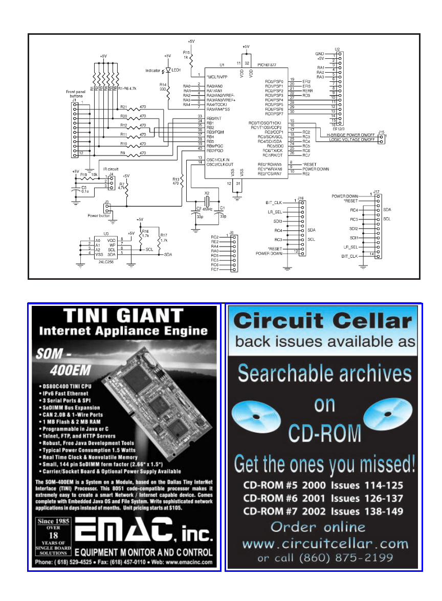
36
Issue 160 November 2003
CIRCUIT CELLAR
®
www.circuitcellar.com
Figure 3—The PIC16F877 is the centerpiece of the design. We can control the entire system through the microcontroller’s I
2
C bus.
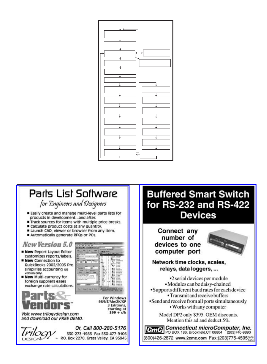
www.circuitcellar.com
CIRCUIT CELLAR
®
Issue 160 November 2003
37
appears to switch at a rate of 384 kHz
nominally, which is eight times over-
sampling for an audio signal sampled at
48 kHz. Presumably, a relatively high-
order noise shaper is used in the
DDX4100 processor to move the quan-
tization noise away from audio frequen-
cies. The overall specification given in
the DDX2060 datasheet is 0.08% typi-
cal THD+noise at an output power
level of 1 W and 0.33% typical at 30 W.
The power efficiency is given as 88%
typical, which means that a device sup-
plying a total of 70 W to one or two loads
only dissipates about 10 W. Because most
program material has a low duty cycle
with respect to full-power operation,
the minimal heatsinking of the output
devices is required, and it can be built
right into the PCB artwork. Apogee has
an entirely separate document devoted
to this aspect of the design. [1]
As you can see in Figure 2, the
DDX4100 digital audio processor incor-
porates numerous functions: it accepts
up to two channels of audio informa-
tion in S/PDIF serial digital format, up
to four channels in I
2
S format, or up to
six channels in AC97 format. If neces-
sary, the digital audio processor sample
rate converts the audio to the 48-kHz
output rate used in the DDX process.
You can use a configurable DSP to
implement volume control, tone con-
trols and parametric equalization, phan-
tom center channel processing, and bass
redirection for an independent subwoofer
channel. The chip can output up to five
channels of audio in the DDX format,
which is suitable for directly driving
DDX amplifier chips, and up to six chan-
nels in I
2
S format for additional process-
ing or conventional D/A conversion.
The chip includes a PLL for clock
multiplication and distribution that can
be driven by internal or external refer-
ences. All of the features of the chip
can be configured via an I
2
C interface.
The amplifier is intended to be able
to handle multichannel audio formats
such as MPEG and AC-3. Because the
DDX4100 cannot decode them, we also
incorporated the Philips SAA2505H
DUET audio processor, which includes
dual DSP cores running at 40 MHz that
can decode both formats in addition to
Figure 4—It helps to create a diagram that shows all
of the possible displays on the VFD. Make sure they
proceed in a logical sequence.
Power-up
Text scrolls on
WELCOME TO
DOLBY DIGITAL !
EEPROM
LOADED
VOLUME = 88
VOL– VOL+ >
*****MUTE*****
SYSTEM SHUTDOWN
GOODBYE !
BASS CONTROL:
TREBLE CONTROL:
BALANCE CONTROL:
DELAY: 54 msec
DEL+ > DEL– >
CHANNEL SELECT
CHANNEL: CH.1
CHOOSE INPUT:
STEREO: < DOLBY:>
SUR. VOLUME: 75
VOL– < VOL+ >
LFE VOLUME: 62
VOL– < VOL+ >
CTR VOLUME: 83
VOL– < VOL+ >
RUN SOUND CHECK?
YES: < NO: >
SOUND CHECK…
LEFT SPEAKER
RIGHT SPEAKER
LEFT SURROUND
RIGHT SURROUND
CENTER SPEAKER
LFE SPEAKER
Displays for 3 s if
up arrow is pressed.
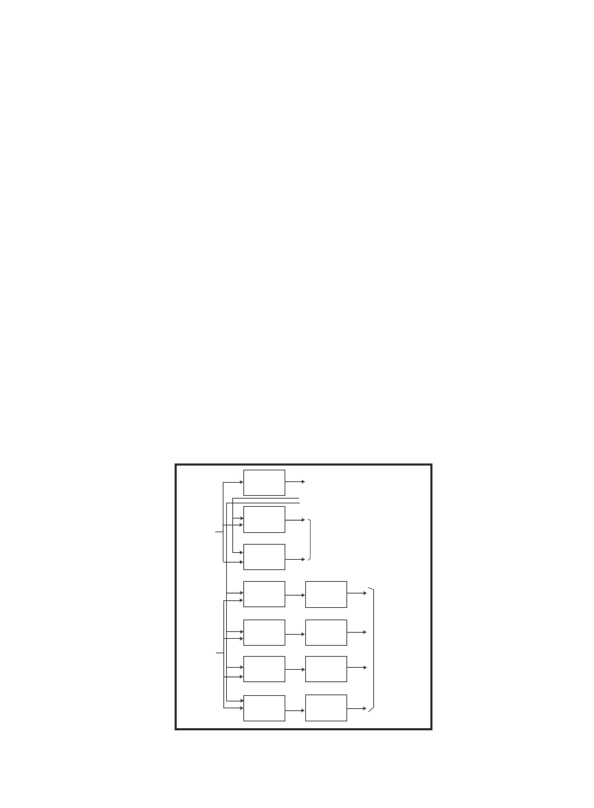
38
Issue 160 November 2003
CIRCUIT CELLAR
®
www.circuitcellar.com
handling conventional stereo PCM. Its
I/O capabilities include two I
2
S inputs
(up to four channels of PCM audio, or
MPEG/AC-3) and four I
2
S outputs
(eight PCM channels). Furthermore, it
has an auxiliary S/PDIF output and is
controlled by an I
2
C interface.
The SAA2505H also provides audio
processing functions, some of which
overlap with the capabilities of the
DDX4100: low frequency enhancement,
bass redirection, karaoke voice mixing,
dynamic range compression, adjustable
time delay for center and surround
channels, digital word length reduction,
audio mute, and error concealment.
Finally, to provide a flexible array of
input options for the amplifier, we
included the CS8415A digital audio
receiver chip, which can select AES/EBU,
S/PDIF, or TOSLINK signals from up to
seven sources. In addition, the chip can
perform clock recovery, separate the
audio data from the auxiliary data chan-
nels in the digital stream, and provide the
audio on an I
2
S output and the auxiliary
data via its I
2
C control interface. We
attached S/PDIF (RCA) connectors to
two of the inputs and TOSLINK (optical
fiber) receivers to another two inputs.
USER INTERFACE
To pull all of these func-
tions together and provide a
unified user interface, we used
a PIC16F877 microcontroller,
particularly because of its
large amount of program
memory and abundance of I/O
pins (see Figure 3). Our code
uses approximately 6 KB of
the 8 KB available in program
memory and all but five of the
I/O pins. It talks to the audio
chips via I
2
C interfaces in
order to determine what kind
of signal is coming in and to
configure the audio chain
appropriately. In addition, it
accepts user commands via
both a set of front panel push
buttons and an IR receiver,
and it displays settings and
status via a front panel vacu-
um fluorescent display (VFD).
The front panel has seven
buttons: Power, Menu Select,
Mute, and four arrows point-
ing left, right, up, and down. The seven
buttons on the universal IR remote con-
trol are used to provide the same inputs.
When the amplifier’s power is off, the
only possible input is to press the Power
switch on the front panel or on the
remote, which powers up the amplifier
and puts the controller in its main loop.
In the main loop, the Power, Menu,
Mute, and volume control functions
(i.e., the left and right arrows) are
immediately accessible. To change
any amplifier parameters other than
volume, the Menu button activates a
series of submenus for bass, treble,
balance, delay, input channel, input
mode, surround volume, LFE volume,
center volume, and channel test. Each
submenu displays an appropriate title
and the current value of the parame-
ter, which you can modify using the
arrow keys (see Figure 4).
DDA users appreciate having a visual
confirmation of the changes they make
to user functions. We chose a VFD
module to implement the user display
because it offers several advantages over
an LCD module or backlit LCD. An
LCD must be viewed up close, at eye-
level, to see the characters. A backlit
LCD improves viewing, although you
still need to be more or less directly in
front of the display in order to see the
characters. Even a small variation in the
angle can result in the appearance of
faded characters (or they can disappear
completely). A VFD is used in most
VCRs, microwaves, and other home
appliances. The VFD’s brightness and
clarity allow you to see the display clear-
ly from across a room and at any angle.
We used a Noritake VFD. The 2 × 16
display module is a drop-in replace-
ment for a typical LCD module (see
Photo 1), which means that we didn’t
need to modify software (or our circuit
diagram) to use the VFD module in
place of an LCD.
Most standard LCDs (as well as the
VFD from Noritake) conform to the
HD44780 model of operation. The
HD44780 is an Hitachi LCD con-
troller/driver. Its specification outlines
initialization procedures for an LCD
module as well as the necessary func-
tions to transmit data for character dis-
play. This specification contained more
information than we needed to initial-
ize our display and send data to it.
Instead, we used the procedure for inter-
facing to Hitachi HD44780-based LCDs
that Myke Predko outlines on his web
site (www.myke.com/engres/lcd.htm).
We interfaced the PIC to the VFD
via four data lines. The
VFD is also capable of
eight-line communication,
but that would require
eight of the PIC’s pins to be
dedicated to VFD commu-
nications. Using the 4-bit
mode allowed us to reserve
four additional pins on the
PICF16877 for future use.
Because of the limitations
of instruction encoding, the
program memory in the
PIC16F877 is divided into
four logical sections, each of
which is capable of storing
2048 words of data. After
our program’s code became
so large that it crossed one
of the boundaries, we had to
rearrange it so that it would
still operate properly. The
problem occurs because the
PIC
CALL and GOTO instruc-
tions can only hold the low-
order 11 bits of the destina-
Switching
regulator
5 V
Switching
regulator
3.3 V
Switching
regulator
5 V
Switching
regulator
29 V
Switching
regulator
29 V
Switching
regulator
29 V
Switching
regulator
29 V
LDO
regulator
27.5 V
LDO
regulator
27.5 V
LDO
regulator
27.5 V
LDO
regulator
27.5 V
To microcontroller
From microcontroller logic on/off
H-Bridge on/off
To output drivers
To digital
audio signal path
13.5 V from
rectifier/filter
34.5 V from
rectifier/filter
Figure 5—The power supply includes two-stage regulation to produce clean power
for the audio output drivers. It also includes features such as software control and
brownout detection.

www.circuitcellar.com
CIRCUIT CELLAR
®
Issue 160 November 2003
39
tion address, which gives 2048 (2
11
) mem-
ory locations that can be accessed direct-
ly. Whenever one of the instructions is
executed, the upper two bits of the 13-bit
program counter are loaded from bits 4
and 3 of the PCLATH register. [2]
When our program grew to more than
2048 words, it crossed over to the next
page of program memory. In order to
jump from one page to a location on a
different page, it is necessary to first load
PCLATH with the page number in bits 4
and 3. We used a macro called LMCALL
to take care of this detail automatically.
IMPLEMENTATION
The majority of the tricky problems
we encountered involved the audio
receiver, decoder, and main CPU
along with its EEPROM. The proper
integration of the units is crucial for
ensuring good performance.
The most important of our recommen-
dations relates to the high-frequency data
and clock lines. In our first design, we
noticed a lot of audio distortion at the
output whenever the unit switched from
simple PCM format into the full six
channels of Dolby decoded information.
The distortion was traced to crosstalk
and interference among the high-frequen-
cy data lines. The first PCB design didn’t
take this possibility into consideration. A
lengthy redesign of the circuit layout and
routing of specific electrical connections
enabled us to generate a clean audio
output that’s free of distortion.
More specifically, we recommend
that you consider several points as
you design the PCB. Carefully lay out
the components to reduce the number
of crossovers of their interconnections
and limit the length of signal lines. Do
not cross signal lines over power traces.
If you need to cross the lines, place a
ferrite chip over the connection. Use
large crosshatched (grid) ground planes
wherever possible in an effort to pro-
vide a clean reference to all of the sig-
nals at all of the points in the design.
Run all critical signals over a continu-
ous ground plane. This will create a
Faraday cage effect and limit the pick-
up of external noise.
The clock lines from the decoder are
of the highest importance and should be
kept as short as possible to avoid inter-
ference. In the board-to-board cables,
run ground lines in parallel between
data and clock lines as a means of can-
celing out crosstalk. Wherever it is not
possible to avoid crossing signal lines,
be sure to do so at a 90° angle so that
the two lines do not couple magnetical-
ly (they cancel out). Additionally, if no
ground plane is opposite this point in
the circuit, use ferrite beads to span
the crossing of the connection.
Read all of the available datasheets
thoroughly. Make sure that you famil-
iarize yourself with the different audio
formats and protocols such as PCM,
SPDIF, and I
2
S.
We spent approximately three weeks
on the design and implementation of the
decoder test board containing the audio
receiver and decoder. Unfortunately,
after testing the implementation, we
were unable to produce an audio output.
Various audio formats were attempted
with no results. After five weeks of test-
ing, an application note from a Phillips
distributor finally arrived containing
information on initializing the

40
Issue 160 November 2003
CIRCUIT CELLAR
®
www.circuitcellar.com
SAA2505H. Two lines that we had left
unconnected were tied to the appro-
priate V
CC
or GND levels, and the
SAA2505H began outputting audio
within minutes. The audio output
from the SAA2505H was now ready to
send data to the DDX-4100 processors
and digital amplifiers.
Another problem that we encountered
was not being able to interface the PIC’s
I
2
C lines (5 V) to the DDX4100 lines
(3.3 V). We solved the problem by using
a MAX3373E bidirectional converter.
POWER SUPPLY
The power supply for the project
underwent many different conceptual
forms, but we ended up with the one
shown in Figure 5. The design requires
three regulated voltage levels: 3.3-, 5-,
and 28-V lines. The 3.3- and 5-V sup-
plies are used in the logic portions of
the circuit. The 28-V line is supplied
to four different points to power the
H-Bridges in the Apogee DDX-2060
digital power driver amplifier ICs.
The logic portion of the power sup-
ply feeds originates from a 9-V second-
ary winding on a toroid transformer.
After full wave rectification, approxi-
mately 13.5 V is sent to three fixed-
value switching regulators. We chose
switch-mode regulators for their wide
voltage input range as well as their
high efficiency. There are two 5-V reg-
ulators and one 3.3-V regulator. One of
the 5-V regulators remains on and con-
tinuously powers the microcontroller.
Originally, the other 5-V regulator
and the 3.3-V regulator were switched
on and off by the microcontroller to
manage the power to the audio cir-
cuits. However, we had problems with
the chips when they were powered
down while the I2C lines were not; it
caused the chips’ input protection
diodes to conduct, and thus powered
up the chip. Consequently, we now
leave the 3.3-V supply on all the time
and only switch off the LCD.
One final feature required in the logic
power supply was a brownout detector
for the DSPs. If the external power sup-
ply ever drops to the point where the 3.3-
V regulator is unable to maintain 97% of
its output, a reset signal is sent to the
DSPs to hold them in Reset mode until
the power reaches an acceptable level
again. Without this feature, the DSP
chips can lock up if a brownout occurs.
The H-Bridge portion of the power sup-
ply provided the largest challenge in the
design. One of the drawbacks of digital
amplification is its low (essentially non-
existent) power supply rejection ratio.
Any variations or noise on the power
supply line directly modulate the output
signal. The voltage to the output drivers
must be exceptionally clean and well reg-
ulated. These four lines are required to
source up to 12 A of peak current when
Photo 1—The Noritake VFD is a drop-in replacement
for standard LCDs. It offers many advantages in line-
powered equipment, where extremely low-power opera-
tion is not required.


www.circuitcellar.com
CIRCUIT CELLAR
®
Issue 160 November 2003
43
the audio drives all the channels to full
output. Therefore, we based the design
on a peak current of 3 A through each
of the H-Bridge’s four branches.
The 28 V originates from a separate
higher-voltage toroid with 24-VAC sec-
ondary windings. After rectification, the
voltage is approximately 34.5 V. We chose
switch-mode regulators because they
can handle input voltages up to 40 V.
However, given the H-Bridge switching
speed, which is on the order of the 400
kHz, there would be undesirable interac-
tions with the 260-kHz switching speed
of the regulators. To fix this problem, we
used a secondary linear low dropout volt-
age (LDO) regulator in series with each
switching regulator. We adjusted the out-
put of these regulators to provide a target
voltage of 27.5 V, which is extremely
close to the ideal 28-V value. This allows
the necessary input voltage headroom for
the LDOs (their maximum input is only
29 V) while maintaining high efficiency.
The microcontroller controls the
H-Bridge power supplies by using the
enable pins on the switching regulators.
The software specifically enables the
logic voltages first and then the H-Bridge
voltage after a short delay. This ensures
that all logic is stable before the micro-
processor enables the audio output.
The reverse occurs for the power-down
sequence, ensuring a quiet power off.
DESIGN FLEXIBILITY
The Dolby Digital Decoder/Power
Amplifier is a highly efficient digital
system that allows for the purest digi-
tal audio signal possible. There are
several ways in which this basic
design can be expanded.
The CS8415A digital audio receiver
allows up to seven inputs, so you can
add additional input connectors to
support extra digital audio sources.
Furthermore, you can change the out-
put drivers to DDX-2100 chips (with
suitable changes to the power supply
and heatsinking), which can supply up
to 50 W per channel, 100 W bridged.
You can add support for the unused fea-
tures of the SAA2505H to the firmware,
including the surround-sound virtualiz-
er, bass management and program down
mixing, and the MPEG 7.1 audio for-
mat, which would allow up to eight
channels of surround sound.
PROJECT FILES
David Tweed was a contributing edi-
tor for this article.
Yoon Cho holds a diploma from
Camosun College, BC and is current-
ly a third-year Computer Engineering
student at the University of Victoria.
You may contact her at
yoon0317@yahoo.com.
Joe Huntley holds a diploma in
Technology in Computer Engineering
from Camosun College. He works as
a technologist at ESI Environmental
Sensors, Canada. You may contact
Joe at huntjoe@hotmail.com.
Greg Nuttall received a diploma in
Electronics Engineering Technology at
Camosun College. He currently works
as a hardware engineer at Coincard
International, and is a fourth-year
Electrical Engineering student at the
University of Victoria. You may reach
him at gnuttall@shaw.ca.
Bryan Olson received a diploma in
Electronics Engineering Technology
from Camosun College. Currently, he
is a marine electronics technician at
V.I. Radar. You may reach him at
bryolson@hotmail.com.
Derek Richardson earned a diploma in
Computer Engineering Technology from
Camosun College. He is a third-year
Computer Engineering student at the
University of Victoria. You may reach
him at richardsonderek@hotmail.com.
REFERENCES
[1] K. Korzeniowski, “Power Stage
Thermal Design for DDX
Amplifiers,” 13000003-02,
Apogee Technology, Inc.,
Norwood, MA.
[2] S. D’Souza, “Implementing a
RESOURCES
Apogee Technology Inc., Direct
Digital Amplification
(DDX):
Pure Digital Sound from Source
to Speaker, 2000.
H. Behrends, “Application of the
SAA2505 Digital Multichannel
Audio Decoder IC (IIC-Control),”
AN990000, 1999.
R. Fischer, “Using the PICmicro
MSSP Module for Master I
2
C
Communications,” AN735,
DS00735A, Microchip
Technology, Inc., 2001.
Noritake Electronics Company,
“Vacuum Fluorescent Display
Module Specification,”
GGM131A, 2000.
SOURCES
CS8415A Audio receiver
Cirrus Logic, Inc.
www.cirrus.com
PIC16F877 Microcontroller
Microchip Technology, Inc.
www.microchip.com
Vacuum fluorescent display module
Noritake Co., Inc.
www.noritake-elec.com
SAA2505H DUET Audio IC
Philips
www.semiconductors.philips.com
Table Read,” AN-556, DS00556E,
Microchip Technology, Inc.,
Chandler, AZ, 2000.
The DDA is a highly flexible audio
system, thanks to its modular design.
It’s a powerhouse in digital audio and
makes an excellent addition to any
home entertainment system!
I

can display a series of options when
the number of lines required for the
options exceeds the number of lines
on the display. Under some circum-
stances some of the options are not
available. (Think of the grayed out
selections in Windows.) Some of the
options are merely lines of text, and
some present data that changes peri-
odically (e.g., time). Other options
present parameters that may be
changed under user control. There are
different units within those parame-
ters (e.g., seconds, percent, degrees
Celsius, and so on).
You should also ask yourself if it is
desirable to change a parameter at any
level of the hierarchy. Is it possible to
place the parameter anywhere on a
line? How can you cater to multiple
languages? Finally, check to see if you
have a timeout on the selection. How
easy would it be to update the software
when the menu structure is changed?
The solutions to these questions are
interrelated. Often, you cannot dis-
cuss one to the exclusion of another.
Each project is unique, so presenting
a generic approach is extremely diffi-
cult, if not impossible. I decided, for
two reasons, to try explaining this
approach while using a real example.
First, it seems to me
that talking about revo-
lutions per minute is
more meaningful than
“Option1Level2.” In
addition to immediately
recognizing a concept
linked to a name, you
44
Issue 160 November 2003
CIRCUIT CELLAR
®
www.circuitcellar.com
I
n a 2002 article titled “Menu
Structures,” Robert Ashby made an
appeal for some thoughts on a method-
ology for implementing menu struc-
tures on embedded systems with limit-
ed resources. [1] Like Robert, I also
thought that there seems to be a dearth
of articles on the subject, and, as I pre-
pared a response to his request, I found
the basis for this article. [2] Several
recent projects have allowed me to dis-
till various methods into one consis-
tent approach for all of my future
needs. This is my fourth attempt!
As society has evolved, the devices
you use have become increasingly
sophisticated because more features
have been added. A microwave oven
has a fairly simple user interface, but
a VCR has several parameters that can
be changed. Cost has dictated that you
use simple display interfaces. Human
logic has allowed you to work with
the limitations by presenting a series
of options. A single selection allows
further refinement to the selection
process until you are left with a single
parameter to change. This selection of
options is intuitive, but the actual
implementation can be confusing. The
flashing 12:00 on many VCRs is evi-
dence of this.
Unfortunately, I cannot
present a method to create
a good human interface.
Aside from being subjec-
tive, it also depends on the
equipment being controlled,
customer requirements, and
user opinion. In this article,
Hierarchical Menus in Embedded Systems
What is the most efficient method for implementing menu structures in embedded systems?
Aubrey had been mulling over this question for several months until he recently worked out
a way to implement a hierarchical menu system that allows you to reuse software for dis-
playing and changing parameters to save ROM space and achieve maximum flexibility.
however, I will show you how to
implement a menu system that will
allow you to reuse the software for
displaying and changing parameters to
save ROM space. More importantly,
the approach will allow you to easily
change the flow of the hierarchy as
the customer and user change their
requirements.
HIERARCHICAL MENUS
Intuitively, you already know how a
hierarchical menu system works (see
Figure 1). The hierarchy of menus
must be defined at the beginning of a
project, because it influences the
approach taken and the flexibility at a
later date. Failure to do so, especially
if your customer doesn’t know what is
possible, will entail additional work
when your client discovers what can
be done. I have found that this
approach allows for changes of that
magnitude with relatively little effort.
You must address several issues
before beginning a design. First, you
must think about how you can select
an option on the display. After you
have made a selection, how can you
back out? Do you go up one level, or
do you go all the way back to level 1?
You must also think about how you
FEATURE ARTICLE
by Aubrey Kagan
Figure 1—Hierarchical menu selection isn’t a difficult concept to grasp.
Level 1
OptionLevel1 1
OptionLevel1 2
OptionLevel1 3
OptionLevel1 4
Level 2
OptionLevel2 1
OptionLevel2 2
OptionLevel2 3
OptionLevel2 4
OptionLevel2 5
Level 3
OptionLevel3 1
OptionLevel3 2
OptionLevel3 3
Level 4
OptionLevel4
www.circuitcellar.com
CIRCUIT CELLAR
®
Issue 160 November 2003
45
Figures 3 and 4 show a portion of
the menu hierarchy that I implement-
ed. Obviously, a real project would
have many more screens. My project
had approximately 70 screens. A sys-
tematic approach is vital for the cod-
ing, documentation, and verification
of the project.
I numbered each screen (i.e., a collec-
tion of lines) for identification. A real
sequence of screens is unnecessary,
because the technique that I used
allows this to be changed, if need be,
which was one of my original require-
ments. I recommend using textual
identifiers associated with the numbers
(e.g., using the C macro
#define to
establish the different screen numbers).
A number of parameters have units,
and the units differ: several are in
floating point, but others are integers,
and some have discrete values with
unique text (e.g., enabled or disabled).
Consistency in the approach to modi-
fication of parameters and the menu
structure will obviously lead to small-
er program size; however, the real
world will conspire to defeat consis-
tency (no doubt a corollary to
Murphy’s Law!).
Unfortunately, in order to explain
the software mechanisms, I need to
familiarize you with the figures. This
should help you understand the flexi-
bility of the approach. I have provided
only the software for the described
also notice other implicit information,
such as the value’s logical maximum.
Second, when you get to the software
implementation, the code has already
been tested and verified, and it is not
a theoretical exercise.
OPTION SELECTION
This project has several interface
requirements: a 4 × 20 LCD; four
input keys, which are used to control
the interface; and screens consisting
of several lines of information. (The
number of lines may exceed the num-
ber of lines on the display.)
The keyboard contains four keys:
Menu, Enter, an up arrow (
↑
), and a
down arrow (
↓
). The Menu function is
used to initiate keyboard entry and
move the hierarchy up one level. The
Enter key will complete a data entry
or accept a menu selection, as well as
allow you to move down a level in the
hierarchy and arrive at a parameter.
The up and down arrow keys are
contextual, because they can be used
to alter parameters, but when there is
a menu selection to be made, the
selection pointer will move in the
selected direction. If the pointer is at
the screen limit, then the screen will
roll in that direction.
A display larger than 2 × 16 intro-
duces a problem. With smaller dis-
plays, only one chunk of information
is visible. More information can be
presented on a larger dis-
play, but not enough for
everything on a single
screen. In order to view all
of the information, the dis-
play screen should have a
four-line window and must
be able to scroll up and
down. Figure 2 depicts this
principle. In order to indi-
cate that there is informa-
tion above or below the
screen view, up and down
arrows are added to the dis-
play when necessary.
A left arrow (
←
) is used to
make menu selections. The
left arrow can move up and
down. When the pointer
moves above or below the
window’s limit, the window
must scroll up or down to
indicate the new selection.
The up and down symbols appear in
the rightmost character position on a
screen line, and the left arrow appears
in the penultimate position. This
means the text is limited to 18 charac-
ters on a 20-character display.
MENU IMPLEMENTATION
Five sublayers of hierarchy in the
menu and parameters, which can be
set in any one of the levels, were also
required in addition to several differ-
ent parameters that had to be changed.
This required different approaches.
Depending on configuration options,
certain lines and parameters do not
necessarily appear because the subse-
quent lines are moved up a level. Note
that multiple languages and a timeout
on keyboard entries are also necessary.
Hierarchy Versn 1.xx
Model X100
Dynamic Reading xx%
06.19.02 16:54
SYSTEM STATUS
USER LEVEL
FACTORY LEVEL
DIAGNOSTICS
BURNER CONTROLS
CONTROL INPUT TYPE
LANGUAGE CONTROLS
SERVICE REMINDER
FULL TANK BLOWDOWN
BLOWDOWN CONTROLS
LOW/HIGH RH ALARMS
DATE/TIME
BURNER 1: ENABLED
BURNER 2: ENABLED
BURNER 3: ENABLED
BURNER 4: ENABLED
BURNER 5: DISABLED
BURNER 6: ENABLED
BURNER 2
ENABLED
Screen 0
Screen 2
Screen 1
Screen 4
Screen 5
Menu
Menu
Enter
Menu
Enter
Enter
Figure 3—You can use the screens to change a binary parameter. When the Enter button is pressed, the selection indicated by
the left arrow is processed.
Selection 1
Selection 2
Selection 3
Selection 4
Selection 5
Selection 6
Selection 7
Figure 2—I’ve displayed a window containing four lines
from a larger screen. When the window includes
Selection 1, the up arrow disappears. When the window
includes the last line of the screen, the down arrow disap-
pears. The window will roll one line down when the left
arrow is in the last line of the window, when the down key
is pressed, and, of course, when the left arrow is not point-
ing at the last line in the screen. Similarly, the window will
roll up one line when the left arrow is in the first line of
the window, when the up key is pressed, and when left
arrow is not pointing at the first line in the screen.
46
Issue 160 November 2003
CIRCUIT CELLAR
®
www.circuitcellar.com
SOFTWARE REALIZATION
Before I go into detail about my
implementation, I will provide you
with an overview of the software
approaches that I used. Although I
used C, it can be easily implemented
in any language, but I hesitate to sug-
gest that assembler is a viable option
for a full-blown system. Many projects
do not have the RAM or ROM to sup-
port this approach in its entirety. It is
possible to use a reduced approach,
keeping in mind that you must tabu-
late everything, because it allows for
versatility in making changes.
Whenever there is a parameter on
the screen, it is incremented or decre-
mented subject to upper and lower
bounds. In addition, some parameters
have a fairly wide range; so modifying
them by one for each key press is
impractical. Holding the key down
will increase the value every 0.5 s by
units, and then tens, hundreds, and
thousands. The transition from units
to tens (and so forth) occurs every 5 s.
PARAMETER DEFINITION
I organized my parameters in a long
list, and gave each one a name and an
combinations; offering much more
would confuse you beyond the point
of no return.
The piece of equipment is produced
as one of two models using the same
controller. One model has three gas
burners. The second model, which is
larger, has six burners. You can enable
or disable each burner. Figure 3
depicts the sequence to do so.
In Screen 0, line 2, the model num-
ber is reported based on a configura-
tion setting. Line 3 includes a display
that continuously displays a change-
able reading. Line 4 is the date and
time derived from an integrated real-
time clock. The colon, which func-
tions as a microcomputer activity
indicator, flashes every second.
In Screen 1, the FACTORY LEVEL
line is visible only when the unit is
being configured in the factory (see
Photo 1). In Screen 2, the LOW/HIGH
RH ALARMS line is visible only
under certain conditions.
Depending on the model type, there
are either three or six burners displayed
on Screen 4. Depending on the configu-
ration, they will display as enabled or
disabled for each of the three or six
burners. Figure 4 describes a sequence
to change a parameter that can vary
between limits. Note that the parameter
changes at a different level in the hierar-
chy than the disable/enable of burner 2
on the extreme right of Figure 3.
All of the displayed messages are
based on the setting of a language
parameter. Although not implemented
in this article, the option is visible on
Screen 2 in Figure 3.
associated number:
#define BURNER1 12
#define BURNER2 13
#define BURNER3 14
The parameters are stored as an array
so they can be accessed using stan-
dard array techniques (e.g., parame-
ters[BURNER]).
Each parameter has a number of
constants associated with it that
determine how it can be changed (i.e.,
maximum value, minimum value, and
step value). A fourth parameter is the
default value, which is normally used
when the unit is first initialized. The
constants are stored in four constant
arrays. During parameter modifica-
tion, while incrementing, the value of
the parameter is not permitted to
exceed the maximum. Similarly, the
minimum defines the parameter’s
lowest possible value. The step value
is the amount the parameter changes,
because the granularity of some
parameters is not one.
MESSAGE LINES
After I had defined and numbered
all of the screens, I collected all of the
possible lines of text. In C, it is possi-
ble to collect the text messages into a
list residing in a two-dimensional con-
stant array. For consistency and ease
of processing, each message should be
of the same length. With multiple lan-
guages I could have used a three-
dimensional array or three two-dimen-
sional arrays. (The implementation of
C that I used ended up with a hybrid
approach.)
Each line in the message list has a
sequential index number associated
with it. This will make it easy to cre-
ate a screen by grouping the index
numbers together to form a screen.
Hierarchy Versn 1.xx
Model X100
Dynamic Reading xx%
06.19.02 16:54
SYSTEM STATUS
USER LEVEL
FACTORY LEVEL
DIAGNOSTICS
FACTORY LOCATION
BLOWER RPM FAULT
BLOWER RESPONSE
RPM TRANSITIONS
CLEAR FAULT HISTORY
RPM TOLERANCE
RPM+/-: 0150
Screen 0
Screen 3
Screen 1
Screen 6
Menu
Menu
Enter
Menu
Enter
Figure 4—A different branch in a parameter selection has a variable parameter.
Listing 1—The messages, which can be entered in any order, are the same length—20 characters.
const unsigned char English[20][30]=
{
//There are 30 messages below of 20 characters in one language
"HIERARCHY Versn ",//0
"MODEL X100 ",//1
"Dynamic Reading ",//2
"SYSTEM STATUS ",//3
"USER LEVEL ",//4
www.circuitcellar.com
CIRCUIT CELLAR
®
Issue 160 November 2003
47
Creating and modifying screens only
requires changing the index number
groupings. The message lines can be
entered in the program in any order so
that adding additional messages does
not introduce a sequencing problem.
This technique allows you to use a
single line in multiple screens. Lines
that differ by only a parameter and
variable (e.g., BURNER x: in Screen 4
and Screen 5 in Figure 3) can be one
line that’s massaged to give the chan-
nel number and add the ENABLED or
DISABLED in Screen 4, or the left
blank in Screen 5.
The @ character is an indicator used
when a parameter must be inserted;
it’s needed when you’re using multi-
ple languages, because the location of
the variable is unlikely to be in the
same place on the line. In English, for
instance, the word “humidity” is
eight letters long, and it would be fol-
lowed by four spaces for a three-digit
humidity number together with the
percentage symbol (%). In German,
the word is dampfleistung, so the
placement of the variable would be
much farther to the right. The pro-
cessing of the line identifies and
removes the symbol and inserts the
value of the desired parameter starting
at the desired location. The message
list is depicted in Listing 1.
SCREENS
One of the requirements of this proj-
ect is to ensure that if an option on a
screen is not enabled, the line or
parameter associated with the option
is not displayed. One way to approach
this is to create an area in RAM to pro-
duce the full screen image (along with
some additional information) regard-
less of whether or not the option is
visible. The associated variables and
parameters should be calculated and
inserted in the appropriate places.
The next step involves an investiga-
tion of the line’s presence. If the line
isn’t required, it’s deleted by shifting
up the lines beneath it. At a later
stage, the image can be transferred
to the display buffer. The up/down
and selection arrows are added when
necessary.
I preserved the image in RAM until
a new screen image was required. This
feature allows other data to supersede
the current display. For instance, if an
alarm is present, it periodically flashes
on the screen via a second display
buffer in RAM. Outputting the origi-
nal screen image without regenerating
the screen restores it. Figure 5 demon-
strates this principle of operation.
For this project, my customer want-
ed the parameters to be visible as he
keys through the hierarchy. Note that
parameters can be changed only after a
password has been entered. This
approach allows the current screen be
maintained in RAM while the display
is occupied with password entry
(through the second display buffer in
RAM). When the password entry is
completed, it’s easy to return to the
current display. All you need to do is
copy the RAM image back to the dis-
play buffer. In the interest of simplici-
ty, I didn’t include these features in
the listings.
As in all projects, you must decide on
certain limits. I opted for a maximum
of 10 lines in any particular screen as
defined in the
MAX_SCREEN_SEL
macro definition. To reiterate, only
four of the display lines can be viewed
Photo 1—The FACTORY LEVEL option was removed
from Screen 1, so the DIAGNOSTICS line moved up.
Screen image
Alternate image
Display buffer
Figure 5—The image to be displayed is prepared in
RAM and then transferred to the display buffer. This
allows the image to be preserved while another mes-
sage (e.g., an alarm or password entry) is displayed on
the screen.
cProcNum[ ] parameter is used to
define the action performed on the
line when the message is copied to
the RAM image (
ProcessLine).
When negotiating through the
menus, pressing the Enter button
takes you to a parameter for change or
display. The parameter name (or
the difference. (One of the lines in the
message array is a row of spaces.)
Some lines may need manipulation
to modify the initial message derived
from the list. For instance, the version
number is added to the message
“HIERARCHY Versn” to produce line 1
on Screen 0 in Figures 3 and 4. The
48
Issue 160 November 2003
CIRCUIT CELLAR
®
www.circuitcellar.com
at any one time. The memory struc-
ture is shown in Listing 2.
Each displayed screen requires some
or all of the parameters to be filled in.
Understanding these parameters is the
key to following what I have done.
cNumberOfLines is the parameter
for the number of lines that make up
a particular screen; it can be between
four and 10. If there are less than four,
the display bulks up by using blank
lines.
cArrowsRequired has to do with
the number of necessary arrows. If the
screen needs arrows, they will be
added. If there are less than five lines,
there won’t be any up or down arrows,
only the selection arrow. In other
words, if this is a zero, a parameter
will need to be changed. If it’s nonze-
ro, there will be another menu screen
as the next level in the hierarchy.
cMsgNo[] is the method by which
lines are grouped together to form a par-
ticular screen. A line index number
forms each element of the array. If there
are less than four lines, the lines should
be padded with blank lines to make up
Listing 2—Every screen must define most of these details to convey which messages are used, whether or
not arrows are needed, what the next state will be, and which parameter to alter.
struct ScreenType {
unsigned char cNumberOfLines;
unsigned char cArrowsRequired;
//Need to display selection arrows
unsigned char cMsgNo[MAX_SCREEN_SEL];
//Message to be displayed
unsigned char cProcNum[MAX_SCREEN_SEL];
//Process to be done on message
unsigned char cParamNum[MAX_SCREEN_SEL];
//Parameter associated with line
unsigned char cNextAction[MAX_SCREEN_SEL];
//Where to go when enter is pressed
unsigned char cAssociatedDisplay[MAX_SCREEN_SEL];
//What to display when enter is pressed
//This can carry a number associated with the line, so that the lines can be
//packed and still correctly identified (it could be eeprom address when the
//line is actually a parameter
};
Why wait? Download AutoTRAX EDA NOW!
Why wait? Download AutoTRAX EDA NOW!
Full Version
$95
Schematic Capture
SPICE Simulation
PCB Layout
Auto-Layout/Router
3D PCB Visualization
Database Support
Schematic Capture
SPICE Simulation
PCB Layout
Auto-Layout/Router
3D PCB Visualization
Database Support
Only
autodesk
®
authorised developer
No Limits!
2.0
It just gets
Better!
To find out more go to
www.autotraxEDA.com
To find out more go to
www.autotraxEDA.com
Drag and drop parts onto your schematic.
Connect them together.
Add virtual instruments such as scopes and function
generators.
Use the PCB design wizard to create your PCB.
Autolayout and autoroute the board.
View the board in 3D.
Output to Gerber and AutoCAD/Solidworks.
Drag and drop parts onto your schematic.
Connect them together.
Add virtual instruments such as scopes and function
generators.
Use the PCB design wizard to create your PCB.
Autolayout and autoroute the board.
View the board in 3D.
Output to Gerber and AutoCAD/Solidworks.
Over 25,000 new users in the last 12 months
Over 25,000 new users in the last 12 months
Full version
to full time-students and schools/colleges (no limits)
FREE
Full version
to full time-students and schools/colleges (no limits)
FREE
Free version available for small scale projects. (pin limited)

50
Issue 160 November 2003
CIRCUIT CELLAR
®
www.circuitcellar.com
address) as defined in the parameter
list is entered in
cParamNum[ ].
There should be an entry for each line
in the display. With a parameter value
of zero, no parameter is used and a
value of 255 (0xff) is for any unused
line. Notice that all the 255 values
should be contiguous to the end of
the array line because this is used to
determine the end of the screen.
The flow of the software through
the hierarchy is set up as a series of
states. (The numbers are used as the
variable
iInterPhase in a switch
construction). When the Enter button
is pressed, the next action is defined
by the
cNextAction[ ] parameter
(
DisplayInterfaceManager).
If this is not a parameter modifica-
tion screen, pressing the Enter but-
ton will invoke a new screen.
cAssociatedDisplay[] will be the
display number that is invoked. There
should be an entry for each line in
the display.
Now let’s consider part of the
Screens[] instantiation of the above
structure as shown in Listing 3. As
you can see, there are eight lines in
the screen. The screen will require
the use of arrows.
The messages are grouped, and if
you check the message listings you
will see that message 7 is BURNER
CONTROLS, and message 8 is CON-
TROL INPUT TYPE, and so on to
make up the display as shown in
Screen 2 in Figure 3.
As you know, the LOW/HIGH RH
ALARMS line is only displayed under
certain conditions. Process 3 (in
ProcessLine) analyzes these circum-
stances. There are no associated
parameters (although there could be
when the project is complete), so the
values are zero, and the line is termi-
nated by 255 (0xff) for the unused
lines. After the Enter button is
pressed for the BURNER CONTROLS
line, the associated manager
(DisplayInterfaceManager) will execute
subtask
BURNER_SELECTION_ENTRY.
After the application is developed fur-
ther, there will be other values for the
remaining lines of the display.
Finally,
BURNER_SCREEN will be
displayed if the Enter button is
pressed on the line. Again, when the
application is further developed, there
will be other values for the remaining
lines of the display.
CONTROL THE PROCESS
A separate task,
DisplayInterfaceManager, pro-
vides the user interface and controls
what appears on the screen and when.
It has many states, which are deter-
mined by the
iInterPhase variable.
Producing something on the screen
is done in two stages. First, the
screen image is prepared in RAM
(
CreateDisplay). At a later stage,
the image that has been created is
transferred to the display buffer with
the arrows added (
TransferDisplay).
The separation of the tasks is neces-
sary to simplify a refresh of the dis-
play when something simple is
changed like the movement of the
selection arrow. The keyboard is also
monitored within these states to
direct the selected displays.
Finally, if a display screen has a

www.circuitcellar.com
CIRCUIT CELLAR
®
Issue 160 November 2003
51
dynamically changing variable, it can
be updated as one of the states (e.g.,
case INITIATE_DISPLAY+1 of the
function). Remember that it takes
time to write to the display, and the
display should not be updated faster
than the update time, or you will only
get partial screens.
At the outset, the initial display
image is created. After that, the user
interaction is roughly the same,
although the key entry may differ for
different menu selections or changing
different parameters. Even though I
have tried to standardize two different
kinds of entries for simplicity, the
advantage of this method is that it is
possible to write numerous tasks to
allow almost any key sequence as need-
ed. The disadvantage is that each sub-
task increases the size of the program,
especially because all keyboard inputs
must be considered in each instance.
When the menu selection leads to
another menu, the process preserves
the relevant details on a dedicated
stack (
PushStack). When returning,
the device (
PopStack) returns to the
selfsame display with the selection
arrow at the same menu entry.
In the case of a selection that leads
to a parameter change, the selected
parameter value (carried from the
cParamNum constant defined in the
Screens[] structure) is loaded into a
temporary location so the modifica-
tion can be ignored by pressing the
Menu button, which will return with-
out modifying the parameter, rather
than the Enter button, which will
return after modifying the value.
The up and down keys also are con-
textual. In a menu selection, a func-
tion (e.g.,
PointerUp, PointerDown)
is invoked to move the selection
arrow and the screen display if neces-
sary. In a parameter change, the up
and down arrows modify a temporary
parameter (e.g., IncreaseParameter,
DecreaseParameter). The value is
transferred back to the parameter
when the Enter button is pressed and
discarded when the Menu button is
pressed.
GENERATE AN IMAGE
When a screen image is generated,
some of the parameters from the
Screens structure are copied to
another structure in RAM (i.e.,
DisplayBuffer), as shown in Listing 4.
Most of the elements are the same
as the Screens structure. The actual
text is copied to the cLine array with-
in the structure.
Additional processing is performed
on the
TransferMsg line for parame-
ter values or other interpretation. If it
is determined that the line should be
removed, the
cParamNum of the asso-
ciated line is changed to 255. When
all of the lines of the particular dis-
play have been processed, the next
stage of the function (
ProcessLine)
compacts the lines upward (based on
whether or not
cParamNum is equal to
255) and overwrites any of the deleted
displays. At that point, the screen
image is created in RAM.
At a later stage, another routine,
TransferDisplay, locates the four
lines to be displayed and copies them
from the image to the display buffer. It
also analyzes which arrows are required
and adds them in the correct locations.
HARDWARE IMPLEMENTATION
At this stage of the game, I will
drop down a level and become more
project-specific. Although the hard-
ware was developed around Rabbit
Semiconductor’s RCM2020 module, I
have tried to make this approach as
universal as possible.
The RCM2020 module includes the
Rabbit 2000 microcomputer (a Z80
derivative), 256 KB of flash memory,
and 128 KB of RAM all on a PCB
measuring less than 2
″
× 2.5
″
. It also
includes I/O lines, an oscillator, and
facilities for battery backing up the
RAM as well as a battery-backed-up
clock/calendar. This is a lot of func-
tionality in a small, reasonably priced
package. Rabbit manufactures and
tests the module, which allowed me
to design a custom, low-volume,
through-hole board with all the advan-
tages of a dense SMD design. The
RCM2020 is mounted on my design
as a mezzanine board.
The display module interface uses
the standard Hitachi HD44780 proto-
col. I have implemented it as a 4-bit
data bus along with the three control
signals on the I/O pins of the Rabbit.
The keyboard input is multiplexed on
some Rabbit I/O pins and consists of
four possible switch closures (or, of
course, a combination of keys).
Listing 4—
DisplayBuffer is the current display in a RAM image. The second element,
cScreenCreatedToGetHere, preserves the screen that was executed to generate this screen so
it can be regenerated if necessary. The third element,
cLine, contains the text of all the message lines.
struct DisplayBufferType {
//This is the memory for the displays sized for the maximum number of rows
unsigned char cArrowsRequired;
//Need to display selection arrows
unsigned char cScreenCreatedToGetHere;
//in order to recreate later
unsigned char cLine[MAX_SCREEN_SEL][21];
unsigned char cParamNum[MAX_SCREEN_SEL];
//Parameter associated with line
unsigned char cNextAction[MAX_SCREEN_SEL]; //where to go when enter is pressed
unsigned char cAssociatedDisplay[MAX_SCREEN_SEL]; //Display to invoke when
//enter is pressed
}DisplayBuffer;
Listing 3—I’ve included the full details for one line of the display. You can add the others as the application
grows.
//USER_LEVEL_SCREEN 2-> Screen[2]
8,
//Equals eight lines
1,
//Arrows required
7,8,9,10,11,12,13,14,0,0,
//Message number
0,0,0,0,0,0,3,0,0,0,
//Processes
0,0,0,0,0,0,0,0,0xff,0xff,
//Associated parameters—0xff used to
//denote line is to be blanked
BURNER_SELECTION_ENTRY,0,0,0,0,0,0,0,0,0,
//
BURNER_SCREEN,0,0,0,0,0,0,0,0,0,
//

52
Issue 160 November 2003
CIRCUIT CELLAR
®
www.circuitcellar.com
External logic provides the enable for
these switches. The software drivers
for these are provided for complete-
ness, but they are not actually within
the scope of this article. The basic
hardware connections are shown in
Figure 6.
DEVELOPMENT ENVIRONMENT
The Rabbit development environment
is implemented on a PC and includes
Dynamic C and a convenient emulator
interface to the RCM2020. You can find
comparisons on the ’Net between
Rabbit’s implementation of C to ANSI C
(groups.yahoo.com/group/rabbit-semi/),
but I’m not going address that issue. I
have tried to keep with standard C;
however, Dynamic C does not allow
for classical multiple module develop-
ment. Using libraries in a manner
similar to multiple modules must be
used to break down large programs.
Rather than having to explain the
library construction (although it is
easy), I resorted to developing this
program as one long module.
In the version of Dynamic C that I
used, there was a restriction that con-
stant arrays be placed in the lower
(i.e., root) 64 KB of flash memory.
With a large number of messages, the
space in the root memory runs out
quickly. The Dynamic C
xstring
function allows the strings to be
placed in extended memory. The
xmem2root function then allows
access to the data as a three-dimen-
sional array. Access to this routine is
in the first section of the
TransferMsg function.
In Dynamic C, it is possible to
change RAM locations while the pro-
gram is running. This is advanta-
geous for this program, because I
have tried to remove it from my
actual hardware, allowing simulation
of switch changes through changing
RAM locations.
USER INTERFACE
The parameters in this application
are grouped into two sets, user and
factory. In the former, you can drill
down the hierarchy and view a partic-
ular setting. In the latter, the option,
and subsequent options and parame-
ters, are only visible if a jumper is
installed on the board. In order to
change a parameter, it must be possi-
ble to invoke a password entry
sequence at any point where a param-
eter is viewed. In this way, you can
see a particular parameter’s setting,
but only authorized users can change
it with a password.
The password entry sequence is not
shown, but it could be introduced as a
step in the keyboard decode when
two keys are simultaneously pressed.
This would then invoke an overriding
sequence that would allow the pass-
word to be entered.
IMPLEMENTATION
I chose to implement the multi-
tasking aspects of the project by
breaking the structure down into
tasks called “phases.” To select a
task, I used a switch statement based
on the
iPhase variable (see Listing 5).
In each task, a number of instructions
are executed until a suitable break
occurs to yield control back to the
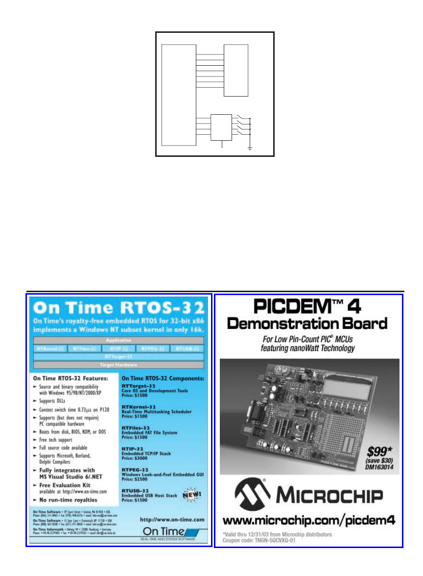
www.circuitcellar.com
CIRCUIT CELLAR
®
Issue 160 November 2003
53
next phase. In many cases, the task
may be divided into subphases and
perhaps subdivided even further.
The tasks that are executed in this
application are the display driver, the
keyboard interface, the display inter-
face manager, and the overall process.
The display driver deals with the
tedious process of sending bytes to the
display module hardware. The key-
board interface monitors key presses
and reports about the inputs.
Obviously, the display manager is the
focus of this article. The overall
process substitutes for most of the
other functions the processor would be
executing in the normal course of
events, which include, in this case,
updating the system time and date.
The display driver is application-spe-
cific. Initially, the display module must
be set to a particular configuration,
which includes the 4-bit format, cursor
style, and data entry. Custom charac-
ters (e.g., an up arrow) are saved as bit
patterns in the RAM on the module.
This provides a simple method of bring-
ing up these characters when desired.
Although it is possible to address
each character on the display individu-
ally, the driver software interfaces via
an array in RAM for each line (e.g.,
cBufferLine1[20]) and a bit on a
status byte that requests an update of
the line (e.g., the WRITE_LINE2 bit on
iStatus). The software scans the four
status bits; when one or more are
active, the associated line in RAM is
output to the display.
The keyboard process maintains a
buffer of three scans of the keyboard
input. As a precaution against contact
bounce, all three must be equal for an
analysis of the input. For any new key-
board input, a timer is initiated so that
the keyboard timeout is refreshed. In
addition, when a key is held down, it
will periodically flag a valid input
(typematic). After a number of these
flags, a variable is incremented to
allow the increment steps to be accel-
erated. In other words, holding the key
down for longer than 1 s results in an
increase of one followed by an addi-
tional increase every 200 ms.
After 10 typematic flags, an output
multiplier is changed, which allows
increments of 10, 100, 1000, and
10,000. This task is used to control
the different timers. Furthermore, it
creates the updated time/date and a
flashing colon between the minutes
and seconds on the bottom line of the
display when the feature is enabled.
PD6
PD5
PD4
PD3
PD2
PD1
PD0
PA7
PA6
PA5
PA4
Rabbit RCM2000
LCD
E
RS
R/*W
D7
D6
D5
D4
Buffer
ENTER
DOWN
UP
MENU
EN
Figure 6—As you study the basic hardware connec-
tions, note that the enable for the keyboard buffer is
generated from some I/O lines and external logic. In
reality, several other groups of inputs are multiplexed
onto PA4–7.
54
Issue 160 November 2003
CIRCUIT CELLAR
®
www.circuitcellar.com
UTILITIES
Some utilities simplify the display
generation. To write a percent value
that is right-justified against the
right-hand side of the screen, use the
PerCent function. To insert a value
(left- or right-justified) starting on a
particular line, use either the
PasteLeft or PasteRight function.
To see how to combine these by insert-
ing a value at the
@ symbol, refer to
case 9 of the
ProcessLine function.
Adding a menu item requires sever-
al steps. First, add the macro for
_ENTRY phase, and then insert this
name in the sixth line (next process)
in the location associated with the
entry in the screen definition. Next,
check if MAX_SCREENS has been
exceeded, update, and add a macro
_SCREEN to describe the new screen.
Insert this name in the seventh line
(associated display) in the location
associated with the entry in the
Screen definition.
The next step is to add the new mes-
sages as necessary and sequentially
number them. Following this, create a
new
_SCREEN entry in the screen.
(Pay attention to the number of lines,
arrows needed, parameters, and so
on.) If the message has a process
associated with it, add a process
number (sequential) and the “case” in
ProcessLine(). Finally, write or
strategically place the _ENTRY in the
DisplayInterfaceManager( ).
Writing your application can get
tricky. Make sure you understand the
subtleties of the program before fol-
lowing the aforementioned steps.
NO MORE HEADACHES
Over the years, the modification of
menus has given me many headaches.
I hope that the system that I have pre-
sented here will preserve what is left of
my sanity and will reduce your devel-
opment and (especially) maintenance
times. I apologize to the C purists for
using of so many global variables. I
guess all the assembly programming I
have done has corrupted my style!
This section of the complete appli-
cation uses 20 KB of flash memory
and the messages use another 15 KB
for the three languages. The RAM
required amounts to 3200 bytes.
These will place significant demands
on a small system’s resources,
because many more menu entries are
likely and the rest of the application
software needs to be completed. Most
of my early experience involved hand-
coding small microcomputers, so I am
aware that this is much larger than a
minimal system can handle.
However, the convenience of a high-
level language and the versatility of
the approach along with the expanded
Aubrey Kagan (P.E.) has 25 years of
experience designing electronic
industrial interfaces and controls. He
earned a B.S.E.E. from the Technion,
Israel Institute of Technology and an
M.B.A. from the University of the
Witwatersrand. His diverse design
experience ranges from projects that
operated miles underground in a
mine to 600 miles above the earth on
the International Space Station. He is
currently a senior design engineer for
Weidmuller Canada. You may reach
him at antediluvian@sympatico.ca.
PROJECT FILES
To download the code, go to
ftp.circuitcellar.com/pub/Circuit_
Cellar/2003/160.
REFERENCES
[1] R. Ashby, “Menu Structures,”
Chip Center, January 2002,
www.chipcenter.com/eexpert/
rashby/rashby054.html.
Structures’ Article,” February
2002, www.chipcenter.com/
eexpert/rashby/rashby056.html.
RESOURCES
———, “RabbitCore 2000,” 001004-
C, www.rabbitsemiconductor.com/
docs/rcm20_devkit_doc.shtml.
SOURCES
HD44780
Hitachi
(650) 589-8300
www.hitachi.com
RCM2020 RabbitCore
Rabbit Semiconductor
(530) 757-8400
www.rabbitsemiconductor.com
capabilities of modern microcomput-
ers have gone a long way to allay my
reservations.
I
Listing 5—With simple cooperative multitasking, it is easy to add additional tasks by adding additional
cases. Remember to increment
iPhase in every task.
while (1)
{
switch (iPhase)
{
case 0:
UpdateDisplay();
break;
case 1:
Keyboard();
break;
case 2:
OverallProcess();
break;
case 3:
DisplayInterfaceManager();
break;
default:
iPhase=0;
break;
}
}

(i.e., absolute zero). Absolute zero is
equal to –273.15°C. In kelvins,
absolute zero is equal to 0K. Really
low temperatures are commonly
measured using the Kelvin scale,
developed by William Thomson
Kelvin in the nineteenth century,
rather than Celsius.
To liquify a gas, you must make it
very cold. A liquified gas stays at its
boiling temperature until it has all
converted back to gas form. Therefore,
liquified gases are a convenient way to
cool other objects to very low temper-
atures. For example, liquefied hydro-
gen, helium, and nitrogen are 20.37,
4.22, and 77.34K, respectively. At
absolute zero, all molecular motion
stops. Absolute zero is not achievable
in the laboratory, although attempts
have resulted in temperatures as low
as 0.00000003K. These sorts of tem-
peratures are not practical. They’re
useful only for research into the basic
properties of matter.
SUPERCONDUCTORS
A superconductor is a material that
has zero resistance to electrical current
when it is cooled to a certain tempera-
ture. The term “superconductor” was
coined by Heike Kamerlingh Onnes in
1911. What’s the big deal about super-
conductors? Electrical resistance caus-
es things to be heavier and less effi-
cient. In other words, it costs money.
So, if you get rid of electrical resist-
ance, you save lots of money.
Superconductors also exhibit
strange properties such as excluding
56
Issue 160 November 2003
CIRCUIT CELLAR
®
www.circuitcellar.com
H
igh-temperature superconductors
and their characteristics simply amaze
me. I hope people who read this arti-
cle will be inspired to experiment
with them. Eventually, I think some-
one will end up developing a room-
temperature superconductor that
changes the world as we know it.
In the 1980s, it looked as though we
were on the brink of a technological
revolution with superconductors. The
advances made with high-temperature
superconductors (HTS) in the ’80s
were so amazing that Nobel prizes
were quickly awarded to several super-
conductor players. The term “super-
conductor” became a household word,
but the excitement has since waned,
at least as far as the general public
goes. However, there’s still great
potential for more advanced supercon-
ductor applications.
ELECTRICAL RESISTANCE
Resistance is the opposition to elec-
trical current flow in a conductor.
Electrical resistance results in heat
generation. To this date, every room-
temperature conductor has some
resistance. Some conductors, such as
gold, have lower resistance than oth-
ers, but the resistance is still there. In
a simple, round wire, the resistance is
proportional to the length of the wire
and inversely proportional to the
cross-sectional area of the wire. If you
want lower resistance wire, you must
make the wire have a bigger diameter.
Making wires have bigger diameters
costs more money because it requires
High-Temperature Superconductor Overview
The expensive cooling processes needed to achieve the superconducting state can make
using superconductors impractical. High-temperature superconductors, on the other hand,
don’t need to be cooled as low, and are therefore less expensive to use. Danny’s review cov-
ers the basics to get you started experimenting with high-temperature superconductors.
more material and increased weight.
On PCBs, the conductive traces
handle current just like wires in larger
systems. If you need to handle more
current, you need to make the traces
wider or the copper thicker. Using
thicker copper on PCBs increases the
cost. And using wider traces takes up
valuable space. If you don’t change to
thicker copper or wider traces when
the current increases beyond the rec-
ommended limits for the PCB design,
you run the risk of burning the traces
like a fuse or at least having hot spots
on the PCB.
Resistance in conductive traces lim-
its the minimum size of integrated
circuits. When you tightly pack the
traces in an integrated circuit, you get
to a point where the traces cannot be
situated any closer because of manu-
facturing limitations, electromagnetic
issues, and so on. The next option is
to make the traces smaller. You then
get to a point where you cannot make
the traces any smaller because of the
current-handling requirements.
Although the heat resulting from
electrical resistance is a nuisance in
many cases, some applications require
it. For example, electric heaters, sol-
dering irons, hair dryers, hand dryers,
and clothes dryers depend on the
resistance of their heater elements in
order to generate heat.
TEMPERATURE REVIEW
There is no limit to how hot some-
thing can get. However, there is a
limit to how cold something can get
FEATURE ARTICLE
by Danny Graves
www.circuitcellar.com
CIRCUIT CELLAR
®
Issue 160 November 2003
57
perature superconductors such as
YBCO is that they are brittle. It is dif-
ficult to make a flexible wire out of
the current HTS ceramic materials. In
addition, ceramics cannot handle the
mechanical stresses of winding elec-
tromagnets. The brittleness is a signif-
icant hindrance to practical usage.
If you have some basic chemistry
experience and equipment, you can
make your own superconductor pellet
from scratch. You can download the
instructions from the web site for the
Oak Ridge National Laboratory, which
is managed by UT-Battelle for the U.S.
Department of Energy. Essentially,
you combine the basic ingredients,
which are fairly inexpensive, grind
them with a mortar and pestle, bake,
and then repeat. The process is fairly
simple and is performed in many high
school chemistry labs.
If you don’t have the inclination to
create a superconductor pellet from
scratch, there are several vendors that
will sell you inexpensive kits that
contain a superconductor pellet ready
to go. Futurescience carries an inex-
pensive kit that contains a small disk
of YBCO, a rare earth magnet, tweez-
ers, Styrofoam cups to hold LN
2
, and
more. You can experiment with the
unusual characteristics of supercon-
ductors such as the Meissner effect
and the zero-resistance effect. The
YBCO disk is mounted via silicone on
a copper pedestal. The silicone allows
the disk to expand and contract with-
out breaking it. The copper pedestal is
for increased heat conduction. With
better heat conduction, you can use
less of the LN
2
. The copper/silicone
pedestal setup also holds the disk at a
good viewing height.
I bought another kit from a different
supplier that was much less well
thought out than the Futurescience kit.
This kit came with the superconductor
disk, a small rare earth magnet, and a
pair of tweezers. Attempts to make the
disk superconduct failed. Apparently, the
YBCO disk was not prepared correctly.
LN
2
is not included with the kits
you can buy off the shelf, but you can
get it from your local industrial/med-
ical gas supplier (see Photo 1). LN
2
usually costs about $2 per gallon in
small quantities. You may have to try
all magnetic fields from their interiors
(i.e., the Meissner effect). So what?
You can make magnets levitate!
Seeing this effect in action will shock
some people the way seeing a UFO or
Bigfoot would. It is truly a strange
effect. It is magic except there is no
trickery by a magician. There is no Uri
Gellar spoon-bending trickery here.
You get conductors to become
superconductors by cooling them.
Many materials will superconduct if
cooled enough. The temperature at
which a material becomes a supercon-
ductor is called the critical tempera-
ture. Unfortunately, the critical tem-
perature for most materials is often
close to absolute zero.
It is interesting to note that many
good room-temperature conductors,
such as copper, gold, and silver, will
not become superconductors (at least
not so far). One theory to explain this
is the lack of a strong interaction
between the electrons and the ion lat-
tice within the material. This lack of
interaction means that the electrons
are freer to move at room tempera-
ture, which results in a good conduc-
tor of electricity. However, the Cooper
pair superconductor theory maintains
that a strong interaction between the
electrons and the ion lattice is neces-
sary for a superconductor.
Nearly 100 years ago, it was discov-
ered that liquid helium could make
superconductors out of materials such
as mercury. Helium was first liquefied
in 1908 by Kamerlingh Onnes. Liquid
helium has a temperature of 4.2K, or
only 4.2K above the coldest tempera-
ture possible. Liquid helium is not
practical or cheap and requires an
expensive refrigeration system.
While the critical temperature of
mercury is 4.2K, the critical tempera-
tures of lead, aluminum, tin, tungsten,
and titanium are 7.2, 1.2, 3.7, 0.015,
and 0.39K, respectively. All of these
materials, like mercury, require expen-
sive, impractical cooling processes to
achieve the superconducting state.
Obviously, to be practical, higher tem-
perature superconductors are needed.
HTS
High-temperature superconductors
exhibit superconductor properties at
much higher temperatures than that
of liquid helium. In fact, inexpensive
and easily obtainable liquid nitrogen
(LN
2
) will sufficiently cool an HTS.
Liquid nitrogen has a boiling point of
–196°C. That’s still cold, but much
easier to accomplish than –273°C. In
addition, nitrogen makes up 80% of
the air we breathe. So, other than the
dangers from the extremely low tem-
perature, LN
2
can be handled safely.
One of the most popular HTS mate-
rials is yttrium barium copper oxide
(YBCO). The lesser-known constituent
element, yttrium, is an abundant ele-
ment. YBCO is a ceramic material
that is an insulator at room tempera-
ture. Yes, that is correct. It is an elec-
trical insulator at room temperature;
however, when you cool it with LN
2
,
YBCO becomes a perfect conductor of
electricity. Strange stuff!
YBCO was discovered at the
University of Houston by a research
team led by Paul C. W. Chu, who filed
a patent application on the same day
that they made the discovery. YBCO
looks nothing like a conductor. It is a
black, powdery material, and if you
check it with a common conductivity
meter, you will see it is truly an insu-
lator at room temperature. However, if
you pour LN
2
over YBCO and check it
with a conductivity meter again, you
will find that it now has become a
conductor.
One drawback to current high-tem-
Photo 1—As the LN
2
warms, it changes back into the
gas state. The loose-fitting top prevents explosion. The
LN
2
lasts a surprisingly long time in this size container.
I got this 10-liter LN
2
container from Airgas in
Clarksville, Tennessee.

one is fixed). When the superconduc-
tor disk is cooled with LN
2
, the mag-
net actually levitates to a position
above the disk from a resting position
on top of the superconductor disk.
The Meissner effect results from the
superconductor material setting up
surface currents that oppose the exter-
nal magnetic field. Because there is no
electrical resistance in the supercon-
ductor, the surface currents can flow
without loss. Therefore, the surface
currents can flow for as long as need-
ed to oppose the magnetic field.
If a magnet is placed on the super-
conductor disk after the disk is
cooled, the zero-resistance effect is
demonstrated as opposed to the
Meissner effect. This will result in the
magnet floating above the supercon-
ductor disk. The physical height at
which a magnet floats above the
superconductor disk because of zero
resistance is higher than the levitation
height that is achieved with the
Meissner effect. Photos 2a and 2b
show the zero-resistance effect in
action floating a neodymium-iron-
boron magnet.
MAGNETIC FIELD PROBLEMS
Placing a superconductor in a mag-
netic field decreases the critical tem-
perature. In fact, if the magnetic field
is strong enough (i.e., critical magnet-
ic field), superconductivity becomes
impossible. Obviously, this fact limits
the practical uses for superconductors
because many applications involve
magnetics.
A group of superconductors known
as Type II superconductors have large
critical magnetic fields that make
58
Issue 160 November 2003
CIRCUIT CELLAR
®
www.circuitcellar.com
several suppliers before you find one
that has a proper experimental/educa-
tional LN
2
container that they will let
you borrow. You can even get a small
quantity of LN
2
in a stainless steel
thermos, although it will not last
long. You cannot seal the thermos to
prevent loss of LN
2
. As the LN
2
changes to the gas state, the pressure
created will burst the thermos; there-
fore, you must leave the thermos vent-
ed. LN
2
can be handled safely if proper
precautions are taken, but you must be
careful with it to prevent injury. If you
search on the Internet for “supercon-
ductors” or “liquid nitrogen,” you will
find several sites that give tips on the
proper handling of LN
2
.
Although LN
2
itself is fairly cheap,
you will find that many dealers want
to charge you $10 to $20 for a few
pints. They lose a bunch of LN
2
when
they try to fill a small thermos, so
they have to charge for the lost mate-
rial too. In addition, the labor of filling
the container with LN
2
may cost more
than the LN
2
itself.
Make sure to pour the LN
2
over the
superconductor disk slowly. If you just
dump a bunch of LN
2
over the super-
conductor, you risk cracking the disk.
Make sure you wear eye protection
when using LN
2
, because things have
a tendency to violently crack when
they are cooled so drastically. If you
don’t wear the glasses, you could end
up with a chunk of YBCO in your eye.
MEISSNER AND ZERO RESISTANCE
A substance that exhibits diamag-
netism opposes a magnet similarly to
the way two magnet faces of the same
polarity oppose each other. A super-
conductor exhibits perfect diamagnet-
ism because it excludes magnetic
fields from its interiors. Any fields
that were present prior to the super-
conducting state are eliminated. When
a superconductor repels a magnet that
is placed on it prior to cooling, it is
called the Meissner effect.
The Meissner effect was named for
one of its discoverers, Walther Meissner.
Meissner and Robert Ochsenfeld dis-
covered the effect in 1933. The
Meissner effect results in a magnet
being levitated above a superconduc-
tor (or vice versa depending on which
them more suitable for practical
magnetic applications. A notable
Type II superconductor is an alloy
consisting of niobium and germanium.
Unfortunately, most Type II supercon-
ductor materials have critical temper-
atures between 10 and 25K.
SUPERCONDUCTOR
APPLICATIONS
There are numerous applications for
superconductors, such as power-line
conductors, super-fast computers,
electromagnetic spacecraft launching
devices, noncontact bearings, and
small, inexpensive medical imaging
equipment. Another application is
Superconducting Quantum
Interference Devices (SQUIDs), which
are used to detect extremely low-level
electromagnetic fields.
The really exciting thing is that the
best applications have not even been
thought of yet. When transistors were
invented, did the pioneers imagine
that they would eventually be shrunk
down to microscopic size and used in
cell phones, GPS receivers, video
games, and PDAs? I doubt it!
So, why would someone want
to learn about superconductors,
experiment with the materials, or
develop practical applications for the
materials? It is fun and interesting
for one thing. Another reason is that
there’s a goldmine to be found in
superconductor application, just like
the goldmine there was for the tran-
sistor back in its early days. It will
probably be some hobbyist in his
garage who makes a big break-
through in new superconducting
materials or applications for existing
Photo 2a—The neodymium-iron-boron magnet is floating about 0.25
″
above a LN
2
cooled yttrium-barium-copper-
oxide superconductor. When I poured about a quarter of a cup of LN
2
into the Styrofoam cup, the levitation effect
amazingly lasted for almost 15 min. before it needed a boost from another shot of LN
2
. b—Here, you can see
another view of a neodymium-iron-boron magnet floating above a LN
2
cooled yttrium-barium-copper-oxide super-
conductor.
a)
b)
www.circuitcellar.com
CIRCUIT CELLAR
®
Issue 160 November 2003
59
materials. The government even
encourages superconductor research.
PATENT INSPIRATION
When you submit a patent applica-
tion, you can request that the applica-
tion be “made special” so that the
patent prosecution is accelerated.
This is called a Petition to Make
Special (PTMS). As slow as the U.S.
Patent and Trademark Office’s
processes are, this is a good thing.
Certain things such as advanced age
of the applicant, environmental appli-
cations, energy applications, illness of
the applicant, and, yes, superconduc-
tivity result in a free PTMS. The fol-
lowing is an excerpt from the USPTO
Manual of Patent Examining
Procedures
(MPEP), chapter 708.2,
regarding superconductivity:
In accordance with the President’s
mandate…the U.S. Patent and
Trademark Office will, on request,
accord ‘special’ status to all patent
applications for inventions involving
superconductivity materials. Examples
of such inventions would include
those directed to superconductive
materials themselves as well as to
their manufacture and applica-
tion…No fee is required.
[1]
Interestingly, the patent process
may have hindered the development
of HTSs. Some companies have tried
to patent the entire class of HTSs.
The legal confrontations resulting
from such legal maneuvers have
stalled some research and the publica-
tion of research results. The commer-
cial potential of high-temperature
superconductors is enormous. When
you have such big commercial poten-
tial, cooperation among individuals
and corporations is naturally hin-
dered. Secrecy is also prevalent and
communication is strategic.
My recent search for “superconduc-
tor” in the patent database on the
USPTO web site (www.uspto.gov)
resulted in 4750 hits. A search for
“YBCO,” under claims, resulted in
199 patent hits. Obviously, there’s
been a lot of superconductor patent
activity during the last 25 years.
FUTURE OF HTSs
I consider room-temperature super-
conductors (or even materials that
will superconduct via freon or dry-ice
cooling) to be the next great techno-
logical leap awaiting mankind. Even
LN
2
-cooled superconductors that can
be easily formed into flexible wires
would be a great leap. Higher tem-
perature superconductors or more
practical applications for current
HTSs could find use in commercial,
military, medical, and spacecraft
applications.
I
Danny Graves, P.E., holds an M.S.E.E.
and is a technical consultant. He cur-
rently performs technical analysis for
patent infringement cases. He also
enjoys technical writing and is in the
process of becoming a registered U.S.
patent agent. You may reach Danny
at dannygraves@bellsouth.net.
REFERENCE
[1] U.S. Patent and Trademark
Office, Manual of Patent
Examining Procedures
, ed. 8,
GPO, Washington, D.C., rev.
February 2003, chapter 708.2.
RESOURCES
Liquid nitrogen container
Airgas
www.airgas.com
Superconductor kit
Futurescience, Inc.
www.futurescience.com
Futurescience, Inc.,
Superconductivity Magnetic
Levitation Demonstration Kit
Model 150
J. Langone, Superconductivity:
The New Alchemy
,
Contemporary Books, Inc., New
York, NY, 1989.
A. Stwertka, Superconductors:
The Irresistible Future
, (Venture
Books) Franklin Watts, Inc., New
York, NY, 1991.
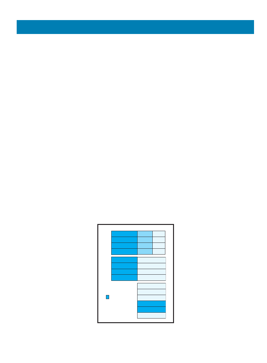
operating modes: Real mode, Virtual 86
mode, and Protected mode. Real mode
is the default: it’s how the chip powers
up, and it’s compatible with the 286
and earlier processors. It’s also called,
with some justification, Brain Dead
mode. Virtual 86 mode is hardly ever
used, and I’ll ignore it for now.
To really enjoy all the 32-bit good-
ness of the 386, you have to enter
Protected mode. Protected mode opens
up an entirely new programming world.
The 386 changes its memory manage-
ment, segmentation is different, new
instructions are available, and hardware
privilege protection is enabled. In short,
when the 386 is in Protected mode, it
behaves like a real 32-bit processor,
not just a faster 8086.
The first thing you’ll notice about
Protected Mode is how roomy it is.
Everything gets bigger. Bigger registers,
bigger memory segments, and a bigger
instruction set. Most registers double in
size to 32 bits (see Figure 1). AX becomes
EAX (extended AX), BX becomes EBX,
and so on. You can still access the low
16 bits as AX, and even the low 8 bits
as AL, just like before. Likewise, the
four address pointers SI, DI, BP, and SP
now have 32-bit extended versions.
That’s easy enough, and it’s a wel-
come change from the cramped regis-
ters of the 8086 and 286. But wait, it
gets better. The 386’s memory seg-
mentation also changes completely in
Protected mode. Segmentation is per-
haps the most hated feature of all x86
processors. Their habit of breaking
memory into 64-KB chunks finally has
60
Issue 160 November 2003
CIRCUIT CELLAR
®
www.circuitcellar.com
B
elieve it or not, there was a time
when Intel’s 386 was the hottest PC
chip around. At 66 MHz, it was blazing-
ly fast. And, best of all, it was a 32-bit
processor. Nervous PC users described
its performance in hushed tones. What
would they do with all that power?
Would it be used for good or evil?
These days, 32-bit processors are,
almost literally, a dime a dozen. Just
counting embedded processors, there are
more than 100 different varieties of
32-bit CPUs, each and every one with
hundreds of happy programmers and
customers. Some cost less than $5.
Others have prices that soar above $500.
Through it all, the x86 family (i.e., 8086,
186, 286, 386, 486, and several flavors
of Pentium and Athlon) has remained
among the most popular. Now that the
386 is too old for PCs, it has found a
new life in embedded systems.
And why not? Intel still makes the
386, and it even produces the special
embedded-only 386EX processor. (AMD
wound down its 386 chips several
months ago.) The 386 may not be the
cheapest, fastest, or most power-efficient
processor around, but it’s familiar to a lot
of programmers, and it’s well supported.
Software, talent, and tools for 386-based
projects are plentiful and often free.
SAME OLD BOSS
Part of the 386’s charm, if I can call it
that, is that it’s part of the x86 family,
which is the best-known chip architec-
ture around. That means the 386 is
upward- and downward-compatible
with older and newer chips from Intel,
Programming the 386 in 32-Bit Protected Mode
Remember when the 386 was the hottest chip on the market? Today, there are dozens of
other 32-bit CPUs, and the 386 is no longer the superlative processor. But wait, there’s a lot
you might not know about the 386. In this article, Jim explains how entering Protected mode
will open your eyes to the 386’s applicability.
AMD, Transmeta, VIA/Centaur,
VAutomation, and other vendors. But
the 386 is also a big step up from its
predecessor, the 286. If you’re an accom-
plished 8086 or 286 programmer, you’ve
got some real treats in store. This
month, I’ll take a look at some of what
makes the 386 so different from all the
other x86 chips that came before it.
The first difference to wrap your head
around is something called Protected
mode. When Intel upgraded from the
16-bit 286 to the 32-bit 386, the compa-
ny had a tough time adding 32-bit good-
ness while still allowing all the old 16-
bit (and 8-bit) code to run. To remedy
this, the 386 now has three different
FEATURE ARTICLE
by Jim Turley
EAX
EBX
ECX
EDX
ESI
EDI
EBP
ESP
31
15
7
0
AH
BH
CH
DH
AL
BL
CL
DL
SI
DI
BP
SP
CS
DS
ES
FS
GS
SS
= New 386 registers
Figure 1—Registers in the 386’s Protected mode
expand to 32 bits with new mnemonics. The older 8-bit
and 16-bit registers are still accessible. Two new seg-
ment registers, FS and GS, have been added.
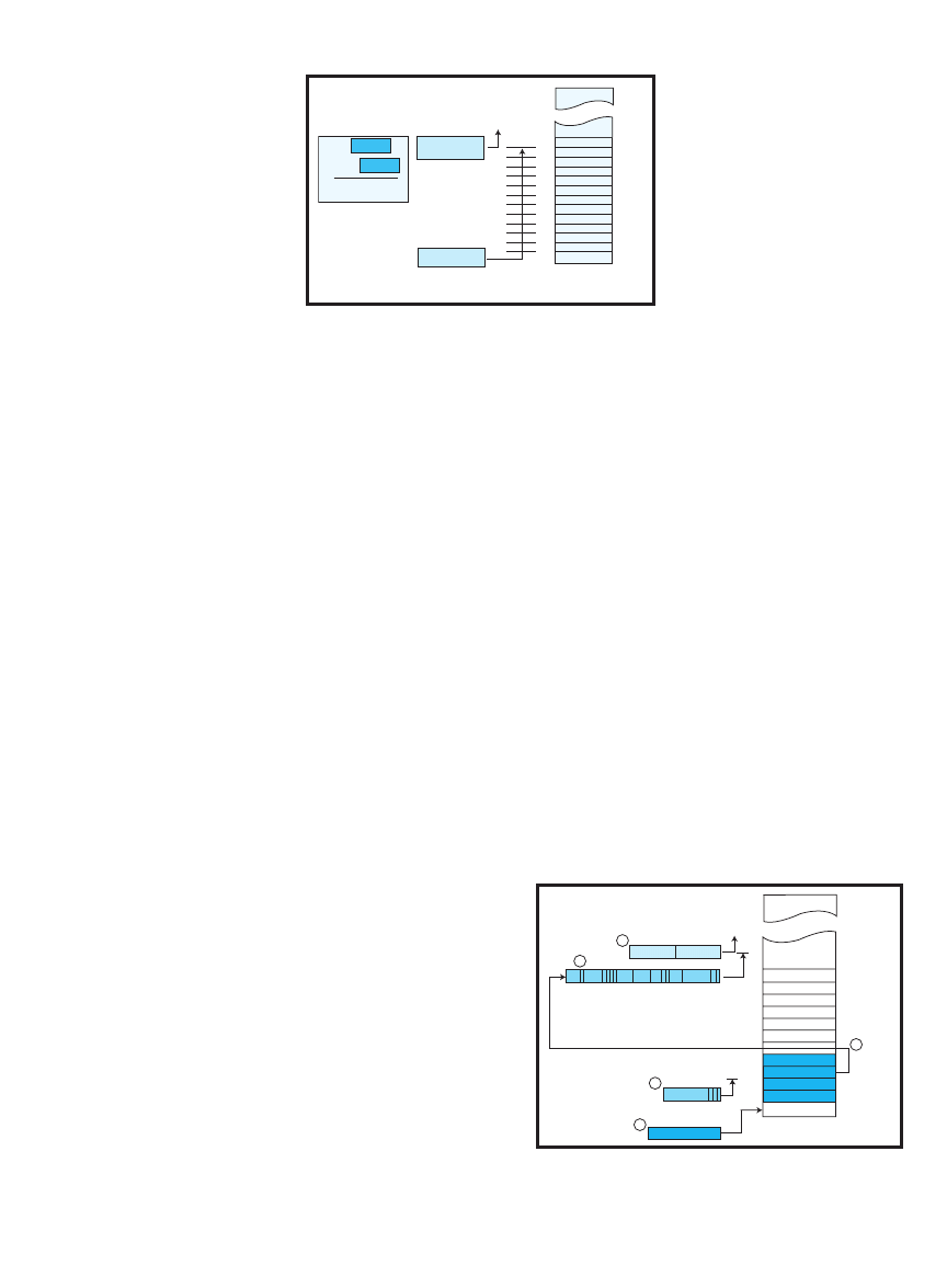
www.circuitcellar.com
CIRCUIT CELLAR
®
Issue 160 November 2003
61
able, and it can be anything from
1 byte to 4 GB. Intel never does
anything the easy way, so natu-
rally the descriptor doesn’t sim-
ply use 32 bits to define the
length of the segment. Instead,
you get 20 bits plus a granularity
bit that controls how the other
20 bits are interpreted by the
processor. The remaining 12 bits
in the descriptor set how the
segment is used, whether it’s
write-protected, how privileged
it is, and even whether or not
the segment is actually present.
And you, dear programmer, get
to set all of these parameters for every
segment (see Figure 4).
Although you will rejoice at the
demise of the 64-KB segment limit,
there are some extremely odd side
effects to the 386’s new type of seg-
mentation. First of all, you must cre-
ate segment descriptors for every area
of memory you’re going to access,
ever. The 386 absolutely will not read
or write any address that isn’t part of
some descriptor. Second, you cannot
simply look at a segment register and
know the segment’s location. Segment
registers are now just pointers into the
descriptor table; they’re not significant
bits of any address. Unless you exam-
ine the descriptor itself and tease the
data out of it, there’s no way to know
where your segment registers are actu-
ally pointing.
Likewise, there’s no way to know
how long a segment is (or where it
ends) without reverse-engineering the
been broken, but it’s a seriously
strange transformation for the
experienced x86 programmer.
Let’s review the old style of x86
memory segmentation. To touch
a byte or word in memory, you
have to load its address into
both a segment register and an
offset register. Then, the proces-
sor shifts the segment register to
the left by four bits (multiplies by
16) and adds the result to the off-
set register, as shown in Figure 2.
The result is your final memory
address. Simple enough, but it
means you have to increment or
reload the segment register every 64 KB.
This granularity usually keeps data
structures, stacks, and code confined
to 64-KB chunks. Getting around this
limitation has been a never-ending
game for most x86 programmers.
WHAT YOU KNOW IS WRONG
All of the old weirdness of memory
segmentation is gone, and it has been
replaced by new weirdness. Figure 3
illustrates how it works in Protected
mode. Are you ready? Take a breath.
First, a new 40-bit register, called
the global descriptor table register
(GDTR), points to the base of a table
somewhere in memory. Each entry in
this table, called a descriptor, is
8 bytes long. Your familiar segment
registers (e.g., DS, CS, ES, and so on)
are now index pointers into this table.
If DS equals zero, it points to the first
(0th) descriptor; if DS equals eight, it
points to the second descriptor (at off-
set 8), and so on.
The descriptor, in turn, holds all of
the information about a memory seg-
ment. The segment’s base address,
length, type (i.e., code, data, or stack),
protection level, and many other
details are all encoded in the descrip-
tor. Thirty-two bits in the descriptor
point to where the segment referenced
in DS actually begins.
Finally, your familiar offset register
(extended SI in Figure 3) determines
the offset into this memory segment.
So, although you still use the register
pair DS:SI as a pointer to memory, the
way it works is utterly different.
For starters, the value you load into
DS has absolutely nothing to do with
the real base address of the segment.
Before, if you loaded 0x400 into DS,
you knew the segment started at
address 0x4000 (i.e., 0x400 shifted left
4 bits). That’s no longer true; DS is
merely a pointer into a table. (To
make matters worse, the location of
the table itself is determined by
another register, GDTR.) It’s the con-
tents of the descriptor DS is pointing
to, not the value of DS itself, which
determines where the segment begins.
Let’s take a closer look at this myste-
rious descriptor that seems to define all
memory on the 386. There must be
exactly one descriptor in the descriptor
table for every segment in memory.
Segments don’t exist without descrip-
tors. The 386 won’t allow you to access
arbitrary addresses in memory unless
you have already defined a descriptor
for that segment. At a minimum, you
should define three segment descrip-
tors—one each for code, data, and stack.
Every descriptor is a
64-bit (8-byte) entry in a
table of similar entries.
Thirty-two bits, or one-
half, of the descriptor set
the base address for that
segment. As you can see,
you can start a segment
at any arbitrary address
anywhere in the 386’s
enormous 4-GB address
space—even an odd
address. No longer do
memory segments have
to start on 16-byte
boundaries.
The length of a seg-
ment is also user-defin-
DS
SI
+
1 3 5 7 4
SI
Offset address
DS
Segment base address
FFFFF
00000
1 2 3 4
1 2 3 4
Figure 2—Old-style memory segmentation relies on a 16-bit segment
register and a separate 16-bit offset register. The actual memory
address is the sum of the offset plus the segment shifted left by 4 bits.
FFFF FFFF
0000 0000
Descriptor
Descriptor
Descriptor
Descriptor
ESI
SI
DS
GDTR
5
4
2
1
3
Figure 3—New-style memory segmentation uses several levels of indirec-
tion to ultimately determine the beginning and end of each memory seg-
ment. Segments can now start (and end) at any arbitrary address in the
386’s entire 4-GB address space.
62
Issue 160 November 2003
CIRCUIT CELLAR
®
www.circuitcellar.com
THE END OF THE WORLD
Have you wrapped your head around
Protected mode memory segmenta-
tion? Good, because I haven’t even
begun to plumb the depths of the
386’s more interesting features.
Briefly, interrupts and exceptions
(faults and failures) get even more con-
voluted. In addition to the large table
of memory descriptors, the 386 also
maintains (courtesy of you, the pro-
grammer) a table of interrupt gates.
Interrupt gates are a bit like an inter-
rupt vector table, with a separate
interrupt vector for each interrupt. In
this case, the vector table is stuffed
with descriptors that add yet another
level of indirection to your interrupt
service routines.
Whenever there’s an interrupt or
fault, the 386 either fetches or gener-
ates a vector, from zero to 255. It uses
that vector as an index into the inter-
rupt descriptor table (IDT), the loca-
tion of which is determined by the
interrupt descriptor table register, or
IDTR. Sound familiar? Each interrupt
descriptor points to a memory seg-
ment descriptor that, in turn, points
to the code for the interrupt service
routine. You did define memory seg-
ments for all your interrupt service
routines, right?
Hold on, there’s more. The 386 can
do its own hardware task manage-
ment. If you’re using a multitasking
operating system, or just want to keep
different tasks away from one another,
the 386 can probably handle it in hard-
ware. You can create elaborate task
state segments (TSSs) that hold all the
dynamic data for each task, and then
descriptor that defines it. You
might run off the edge of the
segment after 64 KB like before,
but probably not. A particular
data segment might be only
100 bytes long, or it might be a
megabyte. There’s no easy way
to know. (By the way, the 386
no longer wraps around the end
of a segment. If you try to read
beyond the last byte of a seg-
ment, wherever that may be,
the 386 aborts your code.)
Increasing the value in DS or
ES doesn’t automatically bump
you up to the next 64-KB seg-
ment of memory, either. Incrementing
a segment register just points to the
next descriptor, which might define a
code segment, a data segment, or no
segment at all. In other words, most
values that you can put into a segment
register are invalid. There’s no way to
simply table-walk through memory by
bumping DS or ES every 64 KB.
Segment descriptors can also define
(in fact, they must define) whether it’s
OK to write into a segment or whether
it’s write-protected. Trying to store data
in a write-protected memory segment,
either accidentally or on purpose, traps
the offending instruction and aborts
your code. This is a great way to pro-
tect sensitive data tables from acciden-
tal overwriting. Finally, code segments
are always write-protected, so say good-
bye to self-modifying code.
Actually, there is a workaround for
self-modifying code, and one that high-
lights still more differences between
the 386 and earlier x86 processors.
You’re more than welcome to create
two different segment descriptors that
point to the same place in memory.
This is known as aliasing, and it’s
extremely useful. For instance, you can
create one descriptor that defines the
memory between 0x1000 and 0x1FFF
as code, and another descriptor that
says the same addresses are data. Load
a pointer to the first descriptor into CS
and a pointer to the second descriptor
into DS or ES, and you can write all
over your own code space. Or, if you
just want to examine your code but
not modify it, create a second descrip-
tor that defines 0x1000 through
0x1FFF as write-protected data.
have the 386 switch between
them on a regular basis. The
processor handles all the load-
ing and storing of variables,
freezing state information, and
so on. It’s hugely complex to
set up but wonderfully useful
when you do. You can even
define your interrupt service
routines as separate tasks and
have the 386 perform an auto-
matic task switch when an
interrupt occurs. The hardware
automatically saves all the
variables and stack informa-
tion for you on every interrupt
without writing a single line of code!
There’s a whole lot more to the 386:
new instructions, new task manage-
ment, new four-level privilege man-
agement, and new hardware features.
There’s enough to fill a fat book,
which is exactly what I did a few
years ago when I developed 386 hard-
ware and software. You may down-
load my book, Advanced 80386
Programming Techniques
, in search-
able Adobe Acrobat format. Visit my
web site, www.jimturley.com, for
instructions.
For more information on the topic,
you can also review Ed Nisley’s Firm-
ware Furnace
series “Journey to the
Protected Land” (Circuit Cellar 48–65).
I
63
56
47
39
16
0
Base address (32 bits)
Length (effectively 32 bits)
Type (code, data, stack, etc.)
Privilege level (0–3)
Limit granularity
16/32-bit segment
Present/not present
Figure 4—Each 386 segment is defined by a 64-bit segment descriptor in
the global descriptor table. Descriptors define the beginning, end, and
characteristics of the segment. Different segment descriptors define the
processor’s code, data, and stack space. Areas of memory not defined by
a descriptor cannot be accessed under any circumstances.
Jim Turley is an independent analyst,
columnist, and speaker specializing in
microprocessors and semiconductor
intellectual property. He is the former
editor of
Microprocessor Report and
host of the annual Microprocessor
Forum and Embedded Processor
Forum conferences. You may write to
him at jim@jimturley.com or visit his
web site at www.jimturley.com.
RESOURCE
J. Turley, Advanced 80386
Programming Techniques
, McGraw-
Hill/Osborne Media, Emeryville,
CA, 1988.
SOURCE
386 and 386EX Microcontrollers
Intel Corp.
(800) 538-3373
www.intel.com

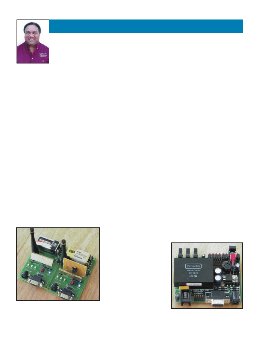
64
Issue 160 November 2003
CIRCUIT CELLAR
®
www.circuitcellar.com
R
F is magical and mysterious, and
so are RF engineers. I truly believe
that RF engineers are really disguised
holdovers from the time of Merlin and
Camelot. Look at what the RF engi-
neering wizards have done to us. Do
you own and operate a cell phone? Is
your pager a constant companion? I’m
from Tennessee, where blackberries
grow on thorny vines along fencerows.
I’ll bet you get e-mail with your
Blackberrys. What about that cordless
phone in your kitchen? These days,
you don’t even need to have wire to
get on an Ethernet LAN. The RF guys
are even messing around with our
food. I went out to eat recently, and
the waitress took my order with a
wireless Palm PC. If cranking magnet-
Using frequency hopping in low-
power radios like the easy-Radio has
its advantages. By hopping at predeter-
mined intervals between preset fre-
quencies in a band of unlicensed fre-
quencies, the chances of interference
from other radio transmissions
decreases. Because the data is dis-
persed over a number of channels, bet-
ter data security is achieved as well.
Over time, the use of frequency hop-
ping reduces the average power level
that is transmitted at a single frequen-
cy, which allows higher peak power
levels than those allowed for single-
band transmitters.
Interfacing to the easy-Radio mod-
ule is easy, because it provides two
handshake lines and a serial interface
running at 19,200 bps. The easy-Radio
handshake lines control the flow of
data to and from the easy-Radio trans-
RF Made Simple
APPLIED PCs
by Fred Eady
ic fields around my food isn’t bad
enough, RF engineering has gone so
far as to leave its mark on the musical
arts. Ask yourself this: When was the
last time you saw a celebrity using a
microphone? Was it wireless? You bet!
Not to be left out of the enchant-
ment, this month I’ve got my eye on
some new data radios and a new
embedded modem. Both the data
radios and the modem are purportedly
“easy” to put into operation. You
know me, when someone claims
something is “easy,” I try it out and
tell you how it went.
EASY-RADIO
Low Power Radio Solutions (LPRS)
has claimed that its easy-Radio allows
you to ignore the radio link and
treat it as if it were a wire. A
simple TTL or RS-232 data
source is all that’s required to
move data from point A to
point B, and vice versa, using a
pair of easy-Radio transceivers.
All of the messy encoding,
decoding, and checksum calcu-
lations are achieved by the
easy-Radio’s internal processor.
The easy-Radio uses frequency
hopping and a maximum of 20
mW of output power to achieve
a range of 500-m line-of-sight.
My 900-MHz easy-Radios hop at
25 times per second over 25 chan-
nels, which, under the control of
the internal microcontroller, is
transparent to the data radio user.
Think of Fred as your own personal litmus test for all of the new embedded technology
thrown your way. This month, he brings the LPRS easy-Radio to the Florida room and puts
it to the test. Read on to find out if his results impress you enough to try your hand at build-
ing an easy-Radio/CH2124 modem station.
Photo 1—I used an unused in-line socket to mount the
PIC12F675 data rate converter module. I took this photo before I
beefed up the voltage regulator on both of the easy-Radio
boards. I used the RS-232 port and the services of RS-232 cir-
cuitry on an unrelated microcontroller-based project board to
feed the remote easy-Radio during development and debugging.
Photo 2—The iModem evaluation board is a great
tool; it saved me lots of time during the development
phase of this project. Everything you need to make the
modem go is on the iModem board.
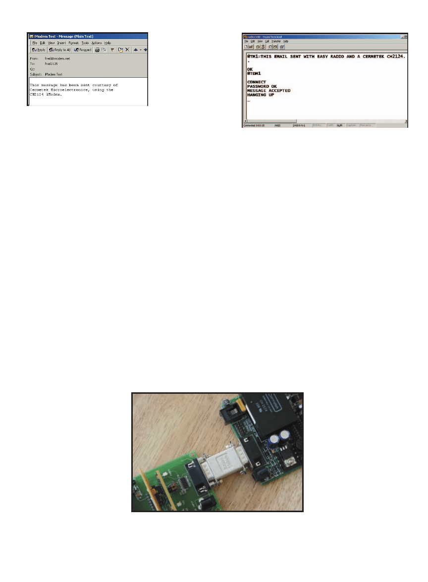
www.circuitcellar.com
CIRCUIT CELLAR
®
Issue 160 November 2003
65
ceiver. If the easy-Radio is busy inter-
nally, the Busy line is asserted. The
easy-Radio’s Busy line alter ego is the
Host Ready input line that informs
the module that the host processor is
ready to transfer data out of the
receive buffer for further processing.
To send data using an easy-Radio,
the host processor checks to see if the
module is busy. If it isn’t, the host
processor feeds a maximum of 80 bytes
of data to the easy-Radio via the
19,200-bps serial link that exists
between the host and the module. If less
than 80 bytes of data are to be transmit-
ted when the host processor has finished
its transfer, two byte times later, the
easy-Radio starts processing the data it
received from the host processor and
activates the Busy output line.
The 2-byte time between the end of
a message that’s less than 80 bytes in
length and the beginning of transmis-
sion processing is called the end-of-
data gap. At 19,200-bps, the end-of-
data gap is 1.04 ms. If the
message from the host proces-
sor exceeds the 80-byte easy-
Radio limit, all of the bytes
beyond the module’s 80-byte
buffer maximum are discard-
ed, and the remaining con-
tents of the easy-Radio trans-
mit buffer are processed for
transmission.
Any easy-Radio module
within range picks up the initi-
ated transmission, drives its
BUSY signal active, and starts
to decode the incoming mes-
sage. The receiving host
processor should then take the
easy-Radio Host Ready line
low. As soon as there is data in
the easy-Radio’s receive
buffer that can be trans-
ferred to the host
processor, it will flow
on the serial link that
exists between the mod-
ule and the host proces-
sor. After all of the data
has been transferred out
of the easy-Radio’s
receive buffer, the easy-
Radio deactivates the
Busy output line.
The host processor
can use the easy-Radio’s
Host Ready line as a
flow-control line. To
stop the flow of data on the serial link
between the host processor and the
easy-Radio module, the receiving host
processor raises the Host Ready line.
Lowering the easy-Radio’s Host Ready
line resumes the data transfer. The
host processor has approximately 2 s
to transfer everything out of the easy-
Radio’s receive buffer before the mod-
ule takes control and flushes the
receive buffer.
DEAD-EASY WIRELESS
Enough theory already. If I’ve missed
something, I’ll cover it as I explain
how to assemble easy-Radio hardware.
I have an easy-Radio evaluation kit
and four easy-Radio 900-MHz hoppers.
The radio boards that came with the
evaluation kit are shown in Photo 1.
This is supposed to be easy, so I’m not
going to design and fabricate any elab-
orate circuit boards or write any fancy
microcontroller firmware to make the
easy-Radios work.
I grabbed a couple of the easy-Radio
hoppers and plugged them into the
evaluation kit radio boards. The evalu-
ation radio boards are simple and con-
sist of an RS-232 converter IC, a low-
power 5-V regulator, configuration
jumpers, a couple of blocking diodes, a
9-V battery clip, an in-line socket for
the easy-Radio module, a wall-wart
jack, an antenna connector, and some
LEDs. The easy-Radio hoppers are
nine-pin, in-line devices that are
keyed for foolproof insertion into the
in-line socket on the evaluation board.
Using my laptop as point A and a
PC as point B, I connected the easy-
Radios to the PCs with a standard
nine-pin, male-to-female cable. I
invoked HyperTerminal on the PCs,
strapped a couple of 9-V bat-
teries on the radio evaluation
boards, and fired them up.
Everything worked as I had
planned. I was able to trans-
mit and receive on both PCs
using the easy-Radio modules.
DEAD-EASY E-MAIL
You guessed it, the easy-
Radios are going to join an
easy-Radio frequency-hopping
network and send whatever
data they share as an e-mail.
Again, there will be no intri-
cate custom PCBs or tricky
software involved in the e-
mail process. I have a proper
English friend, Trevor, who
Photo 3—The text you see in the original e-mail shot is
easily changed using the
@TM1 command. Each
remote easy-Radio can send a custom message by
using this command followed by the microcontroller-
generated text message.
Photo 4—The remote non-modem-equipped easy-Radio generated the entire
line beginning with
@TM1. The end of a message is signaled by a carriage
return dot carriage return. The
@TDM1 was also generated by the easy-Radio
on the non-modem side of the RF link. The rest of the messages, which were
ignored, are from the CH2124. You can see them because I have Serialtest
Async tracing both the CH2124 and the easy-Radio serial connections.
Photo 5—The nine-pin gender changer connects the easy-Radio’s MAX202 to
the iModem evaluation board’s MAX237. After all of the development and
debugging is done, the easy-Radio, PIC12F675, and CH2124 are the only
components needed (in addition to power and a phone line) to generate an e-
mail using the embedded RF link.

66
Issue 160 November 2003
CIRCUIT CELLAR
®
www.circuitcellar.com
uses the term “dead easy” quite often
in our electronic conversations.
Because LPRS is a United Kingdom-
based company, I’m really surprised
that LPRS didn’t call this “Dead-Easy
Radio” (grin).
My web site ISP recently sold all of
its dial-up accounts. Because my e-
mail package is rolled into my web
site contract, I used the dial-up
account for Internet gadget testing
purposes. The new dial-up provider
doubled the price of my dial-up
access, which prompted me to discon-
tinue my dial-up service. When I had
finalized the idea for this column, I
went dial-up ISP shopping. I really
don’t need 199 mailboxes, spam relief,
or high-speed access and a web page. I
simply want to dial up, hook up, and
transfer a few bytes of data between
Internet widgets. The cheapest local
dial-up ISP wanted $12 per month pre-
paid for one year. That’s pretty good,
but I know where I can get the data
service I want for $2 per month with a
local phone number and an easy-to-
use embedded modem to boot.
What you see in Photo 2 is the new
and improved Cermetek CH2124
mounted on an iModem evaluation
board. This version of the CH2124
sends and receives e-mail using the
standard PPP or CHAP authentication
protocols. The circuitry and algo-
rithms within the new CH2124 have
been updated to provide faster and
more reliable dial-up connections.
You don’t need to be intimate with
TCP/IP, SMTP, POP3, or any of those
nerdy protocols to use a CH2124; it is
a set-and-forget, stand-alone kind of
communications device. There are
provisions for interfacing to an exter-
nal microcontroller, but you don’t
need to add one, because the CH2124
can store a canned e-mail message and
send it with the drop of a logic level.
On the other hand, you can get as
nerdy as you wish. For instance, you
can acquire full control of the CH2124
modem and send/receive process
using your hardware, code, and
favorite processor or microcontroller.
Shortly after my regular FedEx rep-
resentative, Chris, delivered my new
CH2124, I plugged it into my iModem
evaluation board, attached a phone
line, supplied some power via a 9-VDC
wall wart, and hit the Send button
(see Photo 2). I spend an inordinate
amount of time in front of my all-in-
one e-mail PC (it sits next to my pro-
duction and design monitors), and I
like to answer e-mail messages as
quickly as I get them. So, I set the e-
mail PC to ask for e-mail messages
every 60 s. I heard the iModem evalu-
ation board/CH2124 combination con-
nect, and, less than 1 min. later, I had
an e-mail from the CH2124.
You’re probably saying, “No way,
Fred!” My initial e-mail from the out-
of-the-box CH2124 is shown in Photo 3.
I told you this would be dead easy, did-
n’t I? All Cermetek CH2124 iModems
are customized and tested before deliv-
ery. To put the CH2124 online in Stand-
Alone mode and deliver the message of
my choice, all I have to do is connect the
iModem evaluation board to a PC run-
ning a terminal emulator program, and
then issue a simple
@T iModem com-
mand to change the canned message.

www.circuitcellar.com
CIRCUIT CELLAR
®
Issue 160 November 2003
67
Everything else needed for sending an e-
mail using the Cermetek $2 ISP and the
CH2124 was already loaded.
DEAD-EASY APPLICATION
Well, almost. This is an embedded
project, and you all know the first rule
of embedded programming (repeat
after me): nothing is free.
I wanted various microcontroller-
supported easy-Radios to report to a
central module that reports to me
with an e-mail message. The idea was
to have the CH2124-equipped easy-
Radio station poll the remote easy-
Radio stations for their data. Every
easy-Radio station within an earshot
picks up a transmission, so I’m also
considering having each radio listen
for a transmission, wait for a predeter-
mined amount of time, and then
transmit its data. Whether to poll or
use a timed sequence for transmission
depends on the application.
In any case, the central CH2124-
equipped easy-Radio station simply
assembles the incoming data from the
radios in the network into an e-mail I
can read and shoots it down the line
using the CH2124. The concept is
simple; however, the implementation
is a click above dead easy. In the
CH2124 and the easy-Radio, we have
two intelligent devices. The easy-
Radio and the CH2124 have serial
ports, which presents Problem 1.
Although both of the smart devices
have serial interfaces, the easy-Radio
serial interface’s speed seems to be
fixed at 19,200 bps. The CH2124
wants to see a 2400-bps serial datas-
tream at its serial interface, which
stands to reason, because it’s an intel-
ligent 2400-bps modem module.
Checking the CH2124 datasheet,
the CH2124 cannot be commanded to
do 19,200 bps at its serial interface. My
goal was to not have a microcontroller
in the CH2124-equipped easy-Radio
station. There’s more than enough
intelligence between the easy-Radio
and the CH2124 to make this RF-to-e-
mail thing happen. Now “dead easy”
has turned into “dead in the water.”
OK, if I have to add a microcon-
troller to solve Problem 1, it’s going to
be an itty-bitty one, and the code is
going to be itty-bitty, too. Because the
CH2124 won’t be retrieving e-mails in
this application, all that’s needed is
to convert the easy-Radio’s 19,200 bps
to 2400 bps, and then feed the low-
ered data rate data to the CH2124’s
2400-bps serial interface.
The production easy-Radio/CH2124
units didn’t need the RS-232 conver-
sion circuitry present on both the
CH2124 and easy-Radio evaluation
platforms. But remember that this was
supposed to be easy, so I verified the
data rate converter hardware and
firmware using the known-good easy-
Radio and known-good CH2124 evalu-
ation hardware already on hand. After I
had a working data rate converter cir-
cuit, I was able to eliminate the RS-232
conversion ICs and stick the itty-bitty
microcontroller between the easy-
Radio and CH2124 serial interfaces.
REMODELING THE BOARD
The blue power indicator LED on
the easy-Radio evaluation boards
stayed. Right now, I don’t know about
the rest of the easy-Radio’s evaluation
board’s power train. There it is, the
potential Problem 2. Easy-Radio engi-
neers warned me that I didn’t have the
latest spin of the easy-Radio evalua-
tion boards. They also said that the
voltage regulator currently on the
evaluation boards wasn’t up to snuff
for the new 900-MHz hoppers.
I’m not planning on adding much
more of a load to the easy-Radio eval-
uation board’s power supply, but I
don’t want to add enough load to
cause a shutdown of the evaluation
board’s on-board 78L05 SMT voltage
regulator. There’s ample ground plane
area on the bottom of the evaluation
board to clear some heatsink space for
a small-package 78M05 voltage regula-
tor that can handle up to 500 mA,
which is more than enough to handle
the easy-Radio hopper module and
what little else I’ll add.
You can power an easy-Radio evalu-
ation board with either a 9-VDC wall
wart or 9-V battery. The evaluation
board’s on-board, 5-V SMT regulator
pre-regulates the incoming 9 VDC pro-
vided by the wall wart. Pre-regulation
is a good thing, because as the average
unregulated 9-VDC wall wart actually
supplies about 12 VDC under light
Listing 1—Most of the work is done by the Custom Computer Services C compiler. The Custom Computer
Services C Compiler Project Wizard generated 99% of the set-up code. I used two serial streams and
wrote only three itty-bitty lines of C source code to turn the itty-bitty PIC into a data rate converter.
#include <12F675.h>
#include <f675.h>
#use delay(clock=4000000)
#fuses INTRC_IO,NOWDT,NOMCLR,NOPROTECT,NOCPD,NOBROWNOUT
#use fast_io(A)
#use
rs232(baud=19200,parity=N,xmit=PIN_A5,rcv=PIN_A4,bits=8,stream=radio)
#use
rs232(baud=2400,parity=N,xmit=PIN_A0,rcv=PIN_A1,bits=8,stream=modem)
void main()
{
setup_adc_ports(0);
setup_adc(ADC_OFF);
setup_counters(RTCC_INTERNAL,RTCC_DIV_2);
setup_timer_1(T1_DISABLED);
setup_comparator(NC_NC_NC_NC);
setup_vref(FALSE);
SET_TRIS_A(0b00010010);
while(1)
{
fputc(fgetc(radio),modem);
}
}
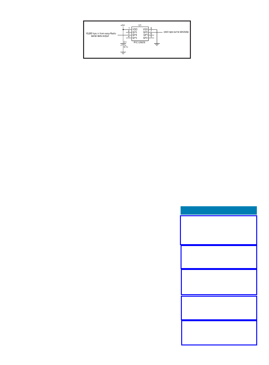
68
Issue 160 November 2003
CIRCUIT CELLAR
®
www.circuitcellar.com
load conditions. The easy-
Radio has an internal 3.6-V
regulator and a 5 V-tolerant
I/O interface. It’s a safer bet
than applying 5 VDC, because
it won’t tax the easy-Radio’s
internal regulator.
The easy-Radio and the
CH2124 are both configured
as DCE, which allows a
straight-through cable to con-
nect either of them to a stan-
dard DTE PC serial port. Because I
wanted to stick with the CH2124 and
easy-Radio evaluation boards, one of
them had to be converted to a DTE
configuration. I’m already chopping
on the easy-Radio evaluation board,
and, in the traditional sense, the
CH2124 evaluation board should be
the DCE device because it holds the
modem, which is considered a DCE
device. So, one of the Easy-Radio eval-
uation board’s serial receive and trans-
mit lines will be swapped to trans-
form the board into a DTE device.
If I poll for data, I will need a micro-
controller on the CH2124 end of the RF
link to initiate the polling sequence. If I
allow the easy-Radios to police them-
selves, I still would require a microcon-
troller on the CH2124 side of the RF
link because I need data rate conver-
sion between the CH2124 and the easy-
Radio module. So, it looks like my no-
microcontroller-at-the-modem-station
idea is a bogus concept. With that, I’ve
got a couple of ideas about which
microcontroller I should use.
My first inclination was to use an
eight-pin PIC12F675 for the data rate
converter. If I go with the little eight-
pin PIC, I’ll have to allow the easy-
Radios to operate on a timed basis,
because I’ll most likely consume all of
the PIC12F675’s processing time con-
verting data rates and transferring
data. To allow the CH2124-equipped
easy-Radio station to poll, I’ll need a
microcontroller with a USART and
USART interrupt capability. That
takes the “easy” out of it, so I’ll go
with the itty-bitty PIC.
The PIC12F675 doesn’t need an
external crystal because it contains an
internal 4-MHz oscillator. All I need
externally to support the PIC12F675
is a 0.1-µF bypass capacitor.
The simplicity of the PIC12F675-
based data rate converter allows you
to mount the PIC12F675 in an in-line
fashion using one of the unused in-line
radio receptacles on the easy-Radio
evaluation board. The evaluation
board is a simple double-sided board,
which allows you to cut and reroute
existing traces to accommodate the
data rate converter’s power and I/O.
All of the data rate conversion is per-
formed on the TTL side of the serial
link. The CH2124 and the easy-Radio
are both designed to use TTL levels on
the serial link and eliminate the need
for RS-232 voltage levels to communi-
cate serially with a host processor.
Normally, the addition of a micro-
controller would allow for the buffer-
ing of the data between the easy-Radio
and the CH2124. In this case, the lit-
tle PIC has no USART or USART
interrupt structure, and I’ve tied up
the PIC12F675’s time to such an
extent that there may not be enough
cycles to perform a buffering opera-
tion without missing an incoming bit.
The solution is to not attempt to
buffer the data with the PIC and allow
the data rate-converted data to flow
freely from the easy-Radio to the
CH2124 modem.
The CH2124 can be instructed to
store a message and transmit the mes-
sage using
@T iModem commands.
Because the channel is always open
between the easy-Radio and the
CH2124, the
@T commands can be
embedded in the incoming datastream
that originates at a remote easy-Radio
station. A typical message from a
remote easy-Radio is shown in Photo 4.
RESULTS
The final prototype of the easy-
Radio/CH2124 modem station is
Fred Eady has more than 20 years of
experience as a systems engineer. He
has worked with computers and com-
munication systems large and small,
simple and complex. His forte is
embedded-systems design and com-
munications. Fred may be reached at
fred@edtp.com.
SOURCES
CH2124 Modem and iModem
evaluation board
Cermetek Microelectronics, Inc.
(800) 882-6271
www.cermetek.com
C Compiler
Custom Computer Services, Inc.
(262) 797-0455
www.ccsinfo.com
easy-Radio
LPRS
+44 1993 709418
www.lprs.co.uk
North American Radio Solutions
(distributor)
(207) 286-1600
www.easyradiousa.com
PIC12F675 Microcontroller
Microchip Technology, Inc.
(480) 792-7200
www.microchip.com
shown in Photo 5. Adding the
data rate converter took a bit
of the “easy” out of the
design, but, as you can see in
Listing 1 and Figure 1, not
much of the simplicity was
destroyed, because the code
and circuitry of the data rate
converter is minimal.
As I worked on this project,
I purposely tried to avoid
designing additional support
hardware, because the products I used
were supposed to make an RF-chal-
lenged (or communications-chal-
lenged) product design engineer’s life
easier. I think the point has been
proven, because both products were
literally ripped out of their boxes and
thrown into service without perform-
ing any kind of configuration or setup.
It cannot get any less complicated and
more embedded than that.
I
Figure 1—I simply inserted the PIC12F675 between the easy-Radio’s 19,200-bps
serial data-out line and the MAX202 RS-232 converter IC’s TTL-side transmit
pin. The PIC12F675 does no buffering and dumps out the data rate-converted
data as soon as it gets it. Character pacing is handled by the remote sending
easy-Radio, because it’s going from a faster to a slower data rate.


70
Issue 160 November 2003
CIRCUIT CELLAR
®
www.circuitcellar.com
M
y wife Beverly leaves our home
each morning at approximately 6:30 a.m.
She is a registered nurse at a local
nursing home. Being somewhat of a
coffee connoisseur, she makes a pot of
java each morning using her secret
recipe. She drinks it straight. I happen
to do the opposite. I can’t tell good cof-
fee from bad coffee, caffeinated from
decaffeinated, so I need to cover up
the taste with milk and heaps of
sugar. Beverly savors her coffee during
the time it takes it to cool to room
temperature. I hate cold coffee; truth
be told, I don’t really like it hot either,
but it is the lesser of the two evils.
Needless to say, I nuke my morning
coffee to get it back up to temperature
after adding milk from the fridge.
One morning, as my mug was riding
on the microwave’s carousel, I gazed
through the protective window as if
staring at an evening’s starry sky. As
the cup of joe passed by the third
time, I turned my attention to the
microwave’s control panel. The array
of flat-panel buttons suggested how far
the microwave has come as an appli-
ance. This was only the second
microwave we had purchased. The
first one had one knob that served as
both the on/off switch and timer.
Gone is the mechanical timer. Today,
timing is done digitally. In fact, using
an embedded microcontroller lends
itself to many other features.
Most microwaves can throttle back
their output power and, thanks to the
carousel, prevent uneven cooking.
However, too many bells and whistles
The OOPic library of predefined
objects makes your design job easier.
You need not worry about a microcon-
troller’s registers and how they must
be coaxed into submission to produce
a function like keypad input. OOPic
has predefined objects. As a designer,
you can select the functions you need
and connect them in a logical way
that’s dictated by your circuit to pro-
duce an OOPic circuit. Objects
include digital I/O, analog I/O,
PWMs/timers/counters, serial com-
munication, keypads, LCDs, and
many others.
Unlike sequential programming
languages, OOPic is event-driven,
which means that independent from
the background code that may be
executing, certain events will trigger
the immediate execution of special
code. The OOPic development sys-
tem runs on all Windows operating
systems. The development system
allows you to combine objects into a
virtual circuit and then compile and
download the resultant code into an
OOPic processor. Yes, the compiled
code requires the use of a special
microprocessor with the OOPic oper-
ating system inside it (starting at
$39). The processor is a flash memo-
ry PIC that’s manufactured by
Microchip and preprogrammed by
Savage Innovations.
OBJECTS
Besides the system object—which
defines the basic properties of the
OOPic operating system—and the
OOPic Eases Programming Headaches
FROM THE BENCH by Jeff
Bachiochi
tend to confuse the average consumer.
So, manufacturers now include specif-
ic buttons such as Popcorn and Baked
Potato. You don’t need to think.
Simply push one button and the
microwave will determine the ulti-
mate program to produce a gourmet
meal, so to speak.
You probably don’t think too much
about your microwave’s small parts
working together behind the scenes.
These parts may be similar to those
used in other appliances, but, in a
microwave, they are dedicated to a sin-
gle function—reheating this morning’s
stale coffee. Good engineering design
makes these small parts invisible.
LANGUAGE TOOLS
If you’re like me, then you are
interested in mechanical things and
don’t like to spend more time than
necessary on the programming aspect
of a project. Software companies are
continuously developing new ways to
help you reduce programming time
and ease the learning curve needed to
pick up a new language. Most pro-
grammers have their favorites and
will die defending them.
The trick for nonprogrammers, or
those of us hackers, is to find a lan-
guage that protects against the raw
bits. Savage Innovations provides a
unique programming environment via
its object-oriented programming inte-
grated circuit (OOPic). OOPic treats
the individual parts (e.g., the carousel,
moisture sensor, and user panel of a
microwave) as objects.
Does programming give you a headache? If so, Jeff recommends OOPic, which allows you
to combine predefined objects (e.g., keypads and LCDs) in a virtual circuit, and then com-
pile and download the code in a special processor. It’s that simple.
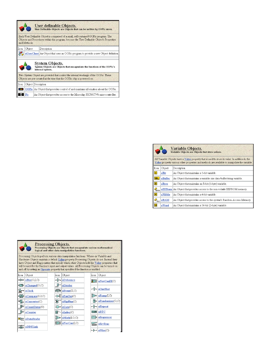
www.circuitcellar.com
CIRCUIT CELLAR
®
Issue 160 November 2003
71
sion, and event-manag-
ing). Refer to Photo 3
for a list of processing
objects.
Hardware objects are
not limited to hardware
functions built into the
microprocessor like,
say, an A/D converter;
they also cover items
that are externally con-
nected, such as a key-
pad. New hardware
objects are constantly
added to the OOPic’s
list of supported
devices. The presently
supported objects are
listed in Photo 4.
OOPic PROCESSOR
The OOPic language is
preprogrammed into a
PIC microprocessor
(OOPicII+ equals ’16F877
in either a 40-pin DIP or
44-pin QFP). The internal
processor RAM has suffi-
cient room in RAM bank 1
for 96 bytes of object
space. (Note that each
instance of an object
requires a few bytes of
object space, generally
3 bytes or less.) The RAM
object directly addresses
the banked RAM.
The flash memory microprocessor
has 256 bytes of inter-
nal EEPROM for non-
volatile storage. Your
compiled application
goes into the external
I
2
C serial E
2
PROM,
which means you can
change programs by
replacing the E
2
PROM.
Your application size
(independent of the
object storage) is based
on E
2
PROM size.
To get started with
OOPic, download the
free compiler and open
it on your PC. The left
side of the screen is a
box in which you can
enter and edit OOPic
commands. The right side of the
screen shows every instance of the
objects you’ve included in the appli-
cation. I’m using the OOPicII+ mod-
ule, which is a 24-pin, DIP-style
pinout that’s compatible with the
Parallax Basic Stamp. The OOPic car-
rier PCB provides access to all of the
I/O. In addition, it has a serial RS-232
DB9 (for connection to your PC), and
can run on a 9-V battery.
Objects have properties associated
with them. Let’s take a look at the
digital I/O bit (
oDIO1) object, which
has six properties: Address, Direction,
IOLine, Nonzero, String, and Value.
An object becomes part of an appli-
cation when you tell the OOPic com-
piler to use it by dimensioning the
object. I named the
0DIO1 object
green, and dimensioned it with the
dim green as new oDIO1 command.
As you can see in Photo 5, an object
appears on the right with the name
green1. When you click on the new
object, a Properties box pops up. The
Properties box is a direct SCP inter-
face to and from the application,
which was compiled and run on the
OOPicII+ using the Make and
Download selection from the File pull-
down menu. (I’ll say more about SCP
later.) As you can see, the Properties
box has been assigned an object
address (by the compiler), but no other
properties have been established.
After the object has been estab-
lished, the properties can be changed
at any time within the application.
All applications begin with a subrou-
tine called
main. I placed three lines
of code there to initialize the proper-
ties of the
oDIO1 objects, IOLine,
user-defined object, there are three
types of OOPic objects: hardware,
processing, and variable (see Photo 1).
Variable objects include instances
for the temporary storage of bit,
nibble, byte, and word data.
Additional variable objects include
a buffer for string/data storage,
access to RAM, and nonvolatile
EEPROM data storage. Photo 2 is a
list of the variable objects.
Processing objects perform data
manipulation functions. The process-
ing objects operate on the values of
variable and hardware objects.
Although the math-processing object
might be the most familiar, other
functions also fall into this category
(e.g., logic, counting, time, conver-
Photo 2—Variable objects store values of various sizes (all versions).
Photo 1—User-definable objects allow you to create your own objects.
Advanced programmers will find this a useful way of adding items neces-
sary for specialized applications. System objects are mandatory for each
application. They set up the groundwork for the operating system based on
the available microprocessor hardware.
Photo 3—The processing objects are used to manipulate the values of other
objects by providing input or receiving output from them.
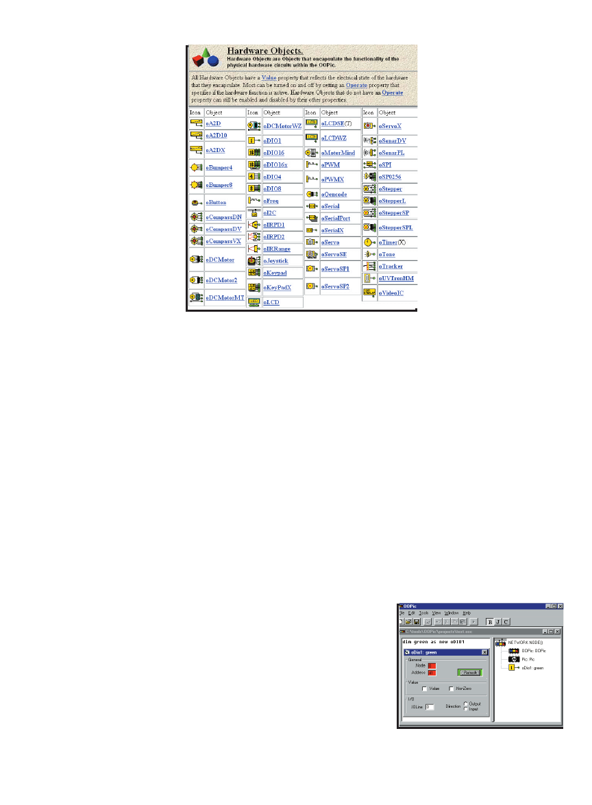
72
Issue 160 November 2003
CIRCUIT CELLAR
®
www.circuitcellar.com
Direction, and Value. The
commands appear in the fol-
lowing format:
object name.property = data
where
green.ioline = 5,
green.direction = 0, and
green.value = 1.
As soon as the code is com-
piled and loaded, it automati-
cally begins execution. Photo 6
shows how these properties
have been initialized, and it
indicates that I/O line 5 is now
an output with a value of 1.
This OOPic has three status
SMT LEDs on the module.
I/O 5 just happens to be the
green LED, which is glowing.
You can click on either the
Value or Nonzero check boxes
in the Properties box to change
their value. The properties box
is a live conduit to and from
OOPic, and your property change will
turn the LED off. This demonstrates
how you have access to the objects
even while the application is running.
The OOPic object has both 1- and
60-Hz clocks available to applications.
The 1-Hz property can be used by any
application. In this example, it’s used
to blink the green LED by adding a
loop and redefining the
green.value
in the following way:
do
green.value = OOPic.Hz1
loop
where the value of the green output
bit 5 is continuously updated with the
value of the 1-Hz clock during the eval-
uation. The application uses a standard
loop process. What happens to the
green.value if the other code within
the loop requires long execution times?
This means that
green.value may
not be updated quickly enough to ade-
quately reflect the 1-Hz rate. Hmm,
hold that thought!
I used two of the five components
that can make up an application—an
object and the main procedure.
Additionally, your application might
contain a sub procedure, an event, and
a virtual circuit. A virtual circuit is
falling edge of the 1-Hz clock
will not cause the event; how-
ever, by creating a virtual
object, by linking the 1-Hz
clock to the event with an
oFanOut object, both the ris-
ing and falling edges can trig-
ger an event object. This is
accomplished by using the
invert property of one of the
oFanOut object outputs.
When the
oFanOut object is
created, it is defined as having
two outputs. By enabling the
.InvertOut2 property of the
second output, it goes through
an additional (virtual) inverter.
The
oFanOut object property
output 1 links to a rising edge
event, and (inverted) output 2
links to a falling edge event.
The sub procedure code for an
event is named with the event
name plus the text
_code. In
Photo 8, one procedure simply
turns on output bit 5 and the other
procedure turns it off. Are you begin-
ning to see the power here?
TOPIC NETWORKING
Based on the Philips’s I
2
C interface,
OOPic takes advantage of the inter-
face’s ability to communicate with
other devices over an open-collector
pair of conductors. The OOPic can
play master or slave device, which
essentially means any OOPic can ini-
tiate communication with another
device or respond to communications
from another OOPic. The
oDDELink
object has the ability to be either the
master or slave by defining the
object’s
.direction property. When
the
.input property is linked to a
the emulation of a physical circuit by
the OOPic operating system. It can
comprise many objects, but at least
one is a processing object.
Let’s go back to the 1-Hz example.
By creating a virtual object (i.e., link-
ing the 1-Hz clock and the output bit
with an
oGate), you can create a situ-
ation in which the output bit gets it
value directly from the 1-Hz value. In
this case, the application is not respon-
sible for updating the
green.value,
and so the
green.value does not rely
on the loop execution speed. Photo 7
shows how the link is accomplished
in a situation in which the loop code
might be slow.
The sub procedure is a block of code
executed on demand from another
part of the application. An event is a
triggering of a sub procedure because
of some action in an object. The event
object is the only object that can cause
a sub procedure to break normal pro-
gram execution, so it is one of the
most powerful objects. Let’s go back
to the green LED example and use the
1-Hz clock to produce an event—well,
actually two events.
The event object is triggered by a
rising edge; therefore, the sub proce-
dure code associated with the event
will occur once every second. The
Photo 4—Many specialized hardware devices are supported in the expand-
ed set of OOPic objects (version B).
Photo 5—A dimensioned object has properties that
must be defined as shown by the
oDIO1:green
properties box.

www.circuitcellar.com
CIRCUIT CELLAR
®
Issue 160 November 2003
73
local object, the object’s value can be
passed to another OOPic, when as
master, it initiates communication
with another OOPic or as a slave
receives a request for the data from
another OOPic. When the
.output
property is linked to a local object, the
object’s value is updated from another
OOPic; as master, it initiates a request
for data with another OOPic or as
slave is given data by another OOPic.
An oDDELink object is required for
the transfer of one value (bit/byte/
word) between any OOPic. By carefully
adjusting the oDDELink object’s proper-
ties on the fly, your application can give
or take values from any other OOPic
located on the same I
2
C interface.
OOPic LIVE
One of the most useful advances in
today’s microcontroller technology is
the ability to monitor what’s going on
inside an application while it’s run-
ning on the actual hardware. An appli-
cation monitor that can be appended
to an application usually handles this.
OOPic uses the primary serial port as
a shared conduit that’s capable of con-
trolling program execution and access-
ing RAM and EEPROM memory. The
hardware port, which defaults as a
serial object, is available to your appli-
cation. It does, however, monitor the
data passing through it for a two-char-
acter escape sequence.
Serial control mode is enabled when
a
\0 escape sequence has been
received. (Note that the second char-
acter—zero in this case—indicates
that the escape sequence is recognized
by all OOPic nodes as a general call,
as opposed to a value of one through
127, which would be recognized only
by that OOPic node.) The command
redirects communications through the
serial control protocol (SCP) module
until it is disabled (i.e., when a
\A
escape sequence is received). All SCP
communications are in a readable
ASC format with single letter com-
mands, single values passed in deci-
mal format, and multiple values
passed in hexadecimal format.
SCP commands can affect the exe-
cution of your application, the appli-
cation itself, or application’s data. You
may download the SCP command list
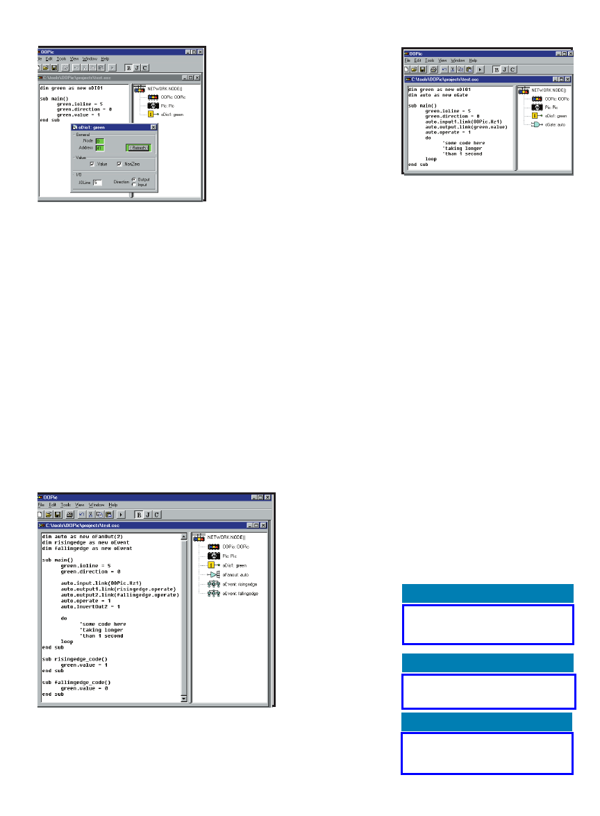
74
Issue 160 November 2003
CIRCUIT CELLAR
®
www.circuitcellar.com
After looking through the prede-
fined objects in OOPic’s library, you
may come to the realization that
many have direct robotic applications.
For those of you who are mechanical-
ly inclined but not necessarily com-
puter literate, OOPic offers you an
opportunity to get your robot moving
and shaking without having to take
classes in microcontroller program-
ming. OOPic user groups are flourish-
ing, which means stability in the
product market. And don’t think that
OOPic can’t meet your needs just
because your project has nothing to do
with robotics. If you’re looking for an
easy way to get the job done, OOPic
offers simplicity with the added
advantage of a short learning curve.
OOPic. Oh-la-la.
I
PROJECT FILES
To download the command list, go
to ftp.circuitcellar.com/pub/
Circuit_Cellar/2003/160.
Jeff Bachiochi (pronounced BAH-key-
AH-key) has been writing for
Circuit
Cellar since 1988. His background
includes product design and manu-
facturing. He may be reached at
jeff.bachiochi@circuitcellar.com.
RESOURCE
OOPic freeware,
www.oopic.com/dload.htm.
SOURCE
OOPic
Savage Innovations
www.oopic.com
because RAM address 0 is available in
multiple banks, each of which con-
tains an address 0. The sub address
also manipulates data so as to mask
and shift individual bits. If accessing
external EEPROM, the sub address is
used as the I
2
C device’s address value.
By presetting these memory descrip-
tors, the Read and Store Memory
commands can access all aspects of
the OOPic memory.
Most of the additional commands
will affect the application’s program
execution. Using SCP commands, you
can start, stop, single-step, branch,
and reset your application. Although
the concepts used to debug an applica-
tion are a far cry from the simplicity
of choosing objects and linking them
together to form their application,
serious programmers will want this
level of sophistication.
ODDS AND ENDS
The order in which objects are
added to your application may have
some impact on the way evaluations
are made. If you are defining virtual
objects, where multiple inputs define
an output, be sure to place them in
such a way that the objects providing
an input are evaluated prior to the
object using the inputs. This is
accomplished by the order in which
they are created in
your application. The
objects are evaluated
in the order they
appear in your appli-
cation. This object
list defines the evalu-
ation order of the exe-
cution loop for your
application.
Your application will
be limited to the num-
ber of objects that can
fit in the 86 bytes of
remaining object
RAM. The requisite
OOPic object requires
10 of the available
96 bytes. Generally,
this isn’t a problem.
The example I used
only required an addi-
tional 11 bytes of
object space.
from the Circuit Cellar ftp site. To read
or write from OOPic memory, descrip-
tive registers must be initialized.
Memory Type refers to the kind of
memory that will be accessed, any of
your application’s object default proper-
ties (in RAM), other internal RAM,
internal EEPROM, or external EEP-
ROM (i.e., your compiled application
code via I
2
C). The Memory Type regis-
ter also indicates whether or not multi-
ple locations will be read, and if the
Memory Address will be automatically
incremented. The Memory Address is a
16-bit value of the address of interest.
A sub address register is needed
when addressing internal RAM,
Photo 6—In theory, every property can be defined by
other objects operating on them; however, it is a good
idea to initialize the properties. In this case, bit 5 will be
used as an output and initialized with a value of one.
Photo 7—By linking the
Hz1 property of the OOPic
object to value property of the green object, the green
output bit will automatically reflect the state of the 1-Hz
OOPic clock without having to evaluate it in a loop.
Photo 8—Events are triggers for a background task that can interrupt normal pro-
gram flow. The
oFanOut object allows a single output to be shared by multiple
objects. One of the
oFanOut properties allows any or all of the outputs to be
inverted. Inverting the 1-Hz clock allows a falling edge to look like a rising edge
and trigger an event. The
risingedge_code and fallingedge_code
events happen on alternate edges of the 1-Hz clock.
CANbus
Starter Packs
available for almost
any board format: PCI, ISA, PCMCIA, PC104,
VME, cPCI, etc. with software for most OS’s
inc. all Windows, Linux, QNIX, etc.
CAN/Ethernet bridges, industrial
computing and automation solutions
Industry leaders worldwide trust and
specify Janz AG’s ISO9000 systems.
Janz AG - a leading CANbus supplier.
S C A L A B L E L E D D I S P L A Y P A N E L S , TEMP-HUMIDITY
MONITORS, T H E R M O C O U P L E P . C . A D A P T E R S , ENVIRONMENT
MONITORING SYSTEMS, EDUCATIONAL SCIENCE PROJECTS,
GRAPHICS SOFTARE, AutoCAD PROGRAMMING COURSE, USB-PIC
BOARDS, FLASH PROGRAMMERS - IF YOU DON’T SEE WHAT YOU
NEED MAYBE WE CAN FIND IT FOR YOU? - JUST ASK FOR ALAN!
by
Janz
for
all
computers
Industrial PCs
Turn your PC into a high-
speed scope. Sampling
rates up to 100MS/s for sin-
gle shot signals (and up to
5GS/s for repetitive signals)
with 12-bit resolution. With
FREE software, your PC
becomes a powerful 2-chan-
nel scope and spectrum
analyzer.
ADC-212/100
$1090
US232 is a 6ft USB-RS232
self-powered converter
cable which instantly and
reliably solves the problem
of laptops with no serial
ports, or legacy RS232
devices that need to be
updated to USB
IN ONLY 5
MINUTES!
Buy in bulk to
update your products - $39!
"After looking at a number of packages
both large and small we have found
TRAKIT
TM
to be the most cost effective
solution for inventory management in the
manufacturing environment available for
the small to medium size company. It
contains most of the commonly used
features of the larger programs as well as
maintaining the user ease of the smaller
programs. Some of the more advanced
features of Trakit are more successfully
implemented than packages costing
many times more. Better and easier to
use than P&V" (S.P. Ltd)
TRAKIT
manufacturing
- Inventory Management
- Bills of Materials
- Build Schedule
- Sales Orders
- Instant Builds
- Purchase Ordering
- Request for Quote
- Reminders
- Reports
K2
9p-9p self-powered RS-422/485 converter
K3
9p-9p isolated RS-422/485 converter
K3-232
9p-9p isolated RS232 converter
K232-ISOL
25p -25p RS232
K422-ISOL
25p -25p RS422
K485-ISOL
25p -25p RS485
KD485-STD
DINrail-mount
RS-232/485/20mA isolators
KD485-PROG
DINrail-mount
RS-232/485/20mA isolators
C-programmable for protocol/MODbus
conversion. Program to convert custom needs.
USB-485i offers self-
powered USB to RS485
conversion with optical
isolation to 1kV. Baud
rates 184bps - 3Mbps.
Link-selectable half-duplex
mode enables the 485
transmit-buffer when data
ready. Three-point isolated
serial communciations.
200 kS/s 12-bit dual-channel USB scope adapter for
PC. Unique software looks like a “Digital Scope” right
on your PC screen! Built-in
squarewave generator.
Weighs less than 8oz so
you can take it anywhere.
Only $189!! For details:
www.usb-instruments.com
USB protocol analyzer displays USB packets sent,
decodes descriptors, detects errors in peripherals or
drivers and measures their performance.
Ideal for anyone developing
USB peripherals,
embedded soft-
ware or drivers.
Software is easy
to use - learn all
about USB. $
8
99!
Make PCs talk I2C easily with this industry-standard
card, available in 2 - 6V bus version for low-volt I2C
systems. Optional WINI2C/PCI software gives you a
windows-interface to develop
and debug I2C bus systems.
Monitor software lets you
transparently monitor I2C bus
activity .
NEW - USB VERSION
UCA93LV: 400kHz monitoring!
Build a custom PCMCIA or CF
card datalogger or controller
- quickly!
Wizard high-level
software completes your
project in hours not weeks.
Store GPS or CANbus data.
TDS2020F is the low-power
controller of choice for sure
LONGEVITY - this one won’t
disappear like so many other
obsolete boards. Ask us why!
Join all the industry leaders who are using this easy-use
USB ic. Single chip USB-232 solution comes with all
Windows/Mac/Linux drivers. UART ASIC-based so no
software development is needed!
Euroquartz is one Europe’s largest manufacturers and
supplier of quartz crystals, oscillators, filters and
frequency-related products. They design & manufacture
a comprehensive range of frequency-related components
including custom-made filters, high
reliability oscillators for defence
applications and radiation tolerant
oscillators for high-altitude apps.
EQ-HM oscillators reduce EMI using
Spread Spectrum Technology
to slowly shift center frequency.
Easily construct small control systems communicating
through Intranet/Internet. BIT2000 is the ideal solution
for process control, building
monitoring, data logging,
alarm systems and other
industrial uses. BIT2000
can communicate with
many types of equipment
through the fast multidrop
RS485 based bus and a
standard RS232 serial port.
At last!
This tiny pocketable USB-based and USB-
powered device is the answer to your need for an eco-
nomical logic analyzer that you can take anywhere.
About the size of a small matchbox, ANT8 can sample
eight channels at up to 500 million samples-per-sec.
ANT8 offers simple or complex
triggering, upgradeable soft-
ware. View the captured eight
digital channel traces on your
PC. Save or print screens for
reference or labnotes! $199!
Manufacturing Software
RS485 factory control
Crystals & Oscillators
Easy USB in one IC!
Basic modules
No USB knowledge required! Byte-
wide ic version FT245BM too!
FT232BM is in the ready-made
US232 cable (USB-serial) - see top
right panel. Instantly update your
legacy serial RS232 products!
PC Scope Adapters
RS232<>422/485
I2C for PCs
Datalogger/Controller
CANbus Cards
Standalone Dataloggers
SM PCB Adapters
USB PC Scope
USB Bus Analyzer
Logic Analyzer
Isolated USB<>RS485
USB-Serial Adapters
BASIC Tigers
are tiny multitasking
modules for quick project development.
Powerful features and low prices make
Tigers a number one choice: super-fast
development cycle, high reliability prod-
ucts, >100,000 instructions/s, up to 38 I/O
lines, A/D, D/A, I2C, SPI, text/graphic LCD
interface.
NOW - SmartCard Interface!
iCOM200
ready-made controller with LCD
and keypad.
Touch240
controller - with
touchpad and LCD display.
Self-contained in 2” x 3” box, these
battery-powered standalone analog
and digital loggers store events,
voltages, currents or pressures for
days to weeks. Download detailed
time and data via serial port and
review results with graphic software
or upload to an Excel spreadsheet.
More details at - www.abidata.be
These SM miniboards have two foot-
prints on either side, allowing you to
use ultra fine pitch SMD components
with a more useful array of 0.1"
spaced holes. 1-to-1 pinout for circuit
probing during design and testing.
Each unique miniboard (pat-pending)
can fit several different devices.
More at www.omega-research.co.uk
Ruggedized Industrial ATX PC systems to suit almost
any budget or PC application.
Easy maintenance, economy
and reliability. $899 version
features AMD Athlon XP1700,
shock-mounted 40GB harddrive.
Lockable front doors prevent
tampering. Full Burn-in and
Test Report with every system.
LED system status indicators.
CE EMC certified. More info at www.amplicon.co.uk
S
A
E
L
I
G
B
R
I
N
G
S
Y
O
U
S
O
L
U
T
I
O
N
S
!

76
Issue 160 November 2003
CIRCUIT CELLAR
®
www.circuitcellar.com
I
’ve definitely got mixed feelings,
bordering on a full-on love/hate rela-
tionship, when it comes to FPGAs. On
the positive side, I consider FPGAs
(more correctly, “programmable logic,”
going all the way back to the seminal
PAL days) one of the most profound
chip concepts, right up there with
heavyweights such as the microproces-
sor and memory. And there’s no doubt
in my mind that the fantastic progress
demonstrated by leading FPGA compa-
nies like Xilinx and Altera will contin-
ue apace. In particular, with Moore’s
Law on their side, FPGAs are poised to
put a world of hurt on ASICs.
Yes, the march of silicon benefits
both FPGA and ASIC suppliers in terms
of gate cost and performance. But it’s
the so-called nonrecurring engineering
(NRE), specifically the mask cost, that’s
the showstopper for ASICs. Mask costs
are shooting up to a million bucks and
beyond with each schuss down the
slope of Moore’s curve past ever-finer
geometries on ever-bigger wafers.
What this all boils down to is an inex-
orable increase in the trade-off volume
BIGGER IS BETTER?
As I wrote back in 1998 (“VolksArray,”
Circuit Cellar
93), the name for Xilinx’s
then new Spartan lineup of FPGAs was
chosen no doubt in light of its mod-
ern interpretation as a “byword for
endurance and rugged simplicity.” Since
then, we’ve seen the Spartan-II, Spartan-
IIE, and now the Spartan-3. The good
news is that the latest parts have all
the bells and whistles.
Naturally, during the five years
since the original Spartan, density has
shot up. Indeed, the smallest Spartan-3
in the eight-chip lineup (see Table 1),
the XC3S50, delivers more gates than
the largest of the originals (50,000 ver-
sus 40,000). At the other extreme, the
XC3S5000 packs a whopping five
million gates!
As an aside, I will not be elaborating
on the controversy over gate counts,
which I’ve referred to in the past as
standing for “gratuitous attempt to
enhance sales.” It’s a lot like MIPS, as
in “meaningless indicator of processor
speed.” The point is, the number of
gates is a highly subjective number
Go Sell the Spartans
SILICON UPDATE
by Tom Cantrell
at which an ASIC makes more sense
than an FPGA as fixed cost (NRE) grows
and variable cost (gates) shrinks. Back
in the ’80s, an ASIC might have been
viable for as few as 50,000 units. Today,
you’re probably looking at 500,000 units
as a reasonable minimum. As the trend
continues, the FPGA suppliers can sim-
ply wait with open arms to welcome
ever-increasing legions of ASIC refugees
fleeing the NRE juggernaut.
Who’ll be left using ASICs? Ironically,
it’s the suppliers of standard chips that
will have the volume to justify appli-
cation-specific IC techniques. And it’s
not just the fabless chip companies
driving the trend. Today, there’s
already a good chance the standard
microcontroller you buy from a com-
pany like Motorola or Philips is in fact
an ASIC that was made in a foundry.
Yes, the future is bright for FPGAs
at the high end, but it’s also the high-
end orientation that is the source of
most of my frustration. Let’s take a
closer look at a modern FPGA and the
tools that go with it, and I think
you’ll see what I mean.
What does the future hold for the modern FPGA? The answer isn’t cut and dry. FPGAs are
massively successful, but as time presses on, they are becoming increasingly complex and
remaining pricey. This month, Tom looks at the direction of the FPGA industry.
System
Max distributed
Number of
Block RAM
Number of dedicated
Number of
Max differential
Max single-
gates
RAM (bits)
block RAMs
(bits)
multipliers
clock mgrs.
I/O
ended I/O
XC3S50
50K
12K
4
72K
4
2
56
124
XC3S200
200K
30K
12
216K
12
4
76
173
XC3S400
400K
56K
16
288K
16
4
116
264
XC3S1000
1000K
120K
24
432K
24
4
175
391
XC3S1500
1500K
208K
32
576K
32
4
221
487
XC3S2000
2000K
320K
40
720K
40
4
270
565
XC3S4000
4000K
432K
96
1728K
96
4
312
712
XC3S5000
5000K
520K
104
1872K
104
4
344
784
Table 1—So many gates, so little time to market. With up to five million gates on tap, the new Spartan-3 lineup puts the ball squarely in the toolchain’s court.
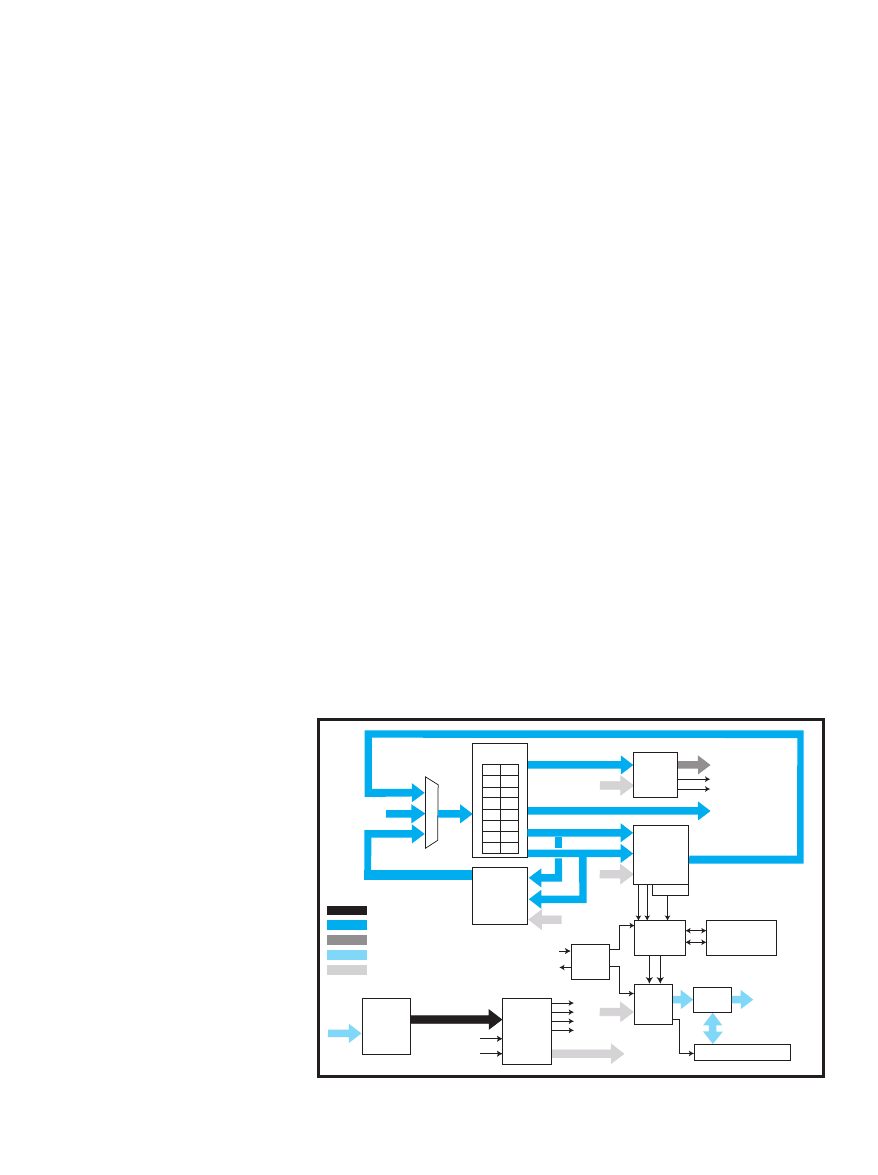
www.circuitcellar.com
CIRCUIT CELLAR
®
Issue 160 November 2003
77
depending on, for instance, how much
logic is used as RAM. But because we’re
comparing apples to apples (i.e., Xilinx
to Xilinx), the company’s own interpre-
tation of “gates” is an acceptable metric.
Beyond lots of gates, the new
Spartan-3 comes with plenty of other
goodies. Probably the most useful is
block RAM, because it eliminates the
need to jury-rig general-purpose logic
(i.e., configurable logic blocks, a.k.a.
CLBs) for use as RAM, which is an
extremely inefficient practice that con-
sumes way too many gates per bit. And
I’m not talking about a few bits of
block RAM either. The XC3S50 starts
the ball rolling with 72 Kb growing to
a whopping 1.8 Mb in the aforemen-
tioned top-of-the-line XC3S5000. A few
million gates here, a few million bits
of RAM there, and pretty soon you’re
talking about real silicon.
Other high-end Spartan-3 features
include up to 104 (!) dedicated multi-
pliers, frequency-synthesizing and
phase-shifting 300-plus-MHz digital
clock managers (DCMs), and digitally
controlled impedance I/O that can
handle a full selection of 23 single-
ended and differential standards.
If some of this seems familiar, that’s
because these “new” features actually
first appeared on the company’s pre-
mium platform Virtex-II FPGAs.
Indeed, the Spartan-3 is much closer
in architecture and capabilities to the
high-end Virtex-II than to the original
Spartan chips whose name it shares.
Although the original Spartan ran on a
single 3.3-V supply and was able to
tolerate standard 5-V TTL connec-
tions, note that Spartan-3 cannot han-
dle 5-V TTL and requires up to three
separate supplies: 1.2 V for the core
logic; 1.2 to 3.3 V for the I/O; and 2.5 V
for special functions.
Similarly, the original Spartan start-
ed at 84 pins and maxed out at 256 for
the package. Spartan-3 offers a 100-pin
option, but only for the entry-level
parts. Beyond that, the smallest pack-
age for the mid-range one million gate
chip is 256 pins, and things escalate
quickly from there. For instance, if
you want the top-of-the-line, four or
five million gate Spartan-3s, you’re
getting a part with at least 900 pins
whether you need them or not.
I can understand that the Spartan
marketing concept as kind of a loss-
leader version of Virtex-II, much as a
Chevy looks a lot like a Cadillac
under the hood, but dare I say that the
rugged simplicity theme is a bit of a
stretch? All the more ironic to note,
Spartan-3 is actually manufactured
using a state-of-the-art, 90-nm process
versus 150 nm for Virtex-II.
TOOL TIMEOUT
Configuring the original programma-
ble logic PAL chips was easy. Type in a
few sum-of-products logic equations
and let a simple PALASM program
crunch ’em a bit and spit out a few bits
of fuse map. And, of course, the origi-
nal FPGA schematic capture methods
using MSI TTL-like macros (e.g., regis-
ters, decoders, multiplexers, etc.) were
familiar to any board-level designer.
Later, core generator enhancements
based on higher-level parameterizable
functions such as arbitrary width
timer/counters and multiplier/accumu-
lators made life easier.
But between the ASIC-killer aspira-
tions and incredible density boost, now
you have a situation where FPGA tools
are as complicated as the ASIC tools of
yore. Indeed, with big-ticket ASIC tool
suppliers like Cadence, Synopsys, and
Mentor Graphics branching into FPGAs,
an FPGA designer may literally be
using the same tools as a chip design
guru at Intel or Motorola. And that
includes making the big post-schematic
era move to logic synthesis using hard-
ware description languages (HDLs) like
Verilog or VHDL.
It gets even more complicated with
the emergence of on-chip CPU cores,
such as the hard PowerPC core (make
that cores, up to four of them) on the
Virtex-II Pro and the 32-bit MicroBlaze
soft core. You can imagine the chal-
lenges associated with designing, simu-
lating, and debugging a lash-up of CPUs
and OSs buried in millions of gates and
bits hidden behind hundreds of pins.
The original inspiration for this arti-
cle was sparked by my encounter with
the new Xilinx embedded development
kit (EDK) at the Spring ESC show in
San Francisco. The purpose of the EDK
is to fill the hardware-software code-
sign gap with a tool that helps config-
ure and integrate the major hardware
and software functional blocks that
comprise an FPGA-based System-on-a-
Chip. Originally, I had planned to actu-
ally hook up a board and play around
with this latest-and-greatest FPGA
setup, but, discretion being the better
part of valor, it wasn’t long before I
retreated from that worthy goal.
In retrospect, the fact that the pack-
age arrived with five CDs was perhaps
the first hint that I was in trouble.
ALU
Arithmetic
logical
shift
rotate
PARITY
sF s7
sE s6
sD s5
sC s4
sB s3
sA s2
s9 s1
s8 s0
16 Registers
8 bits
Interrupt
control
ZERO and
CARRY
flags
Interrupt
shadow flags
Program
counter
Program counter stack
Program
flow
control
Operational
control
and
instruction
decoding
Program
ROM/RAM
1024 words
8-bit Data path
10-bit Program address
Constants
8-bit Port address
18-bit Instruction word
pp
OUT_PORT[7:0]
PORT_ID[7:0]
READ_STROBE
WRITE_STROBE
kk
ss
INSTRUCTION[17:0]
aaa/pp/ss/kk
aaa
INTERRUPT
INTERRUPT_ACK
ADDRESS[9:0]
RESET
CLK
IN_PORT[7:0]
Port
address
control
Scratch pad
memory
64 bytes
Figure 1—Here’s the PicoBlaze—in this case, the KCPSM3 version—at a glance. And that’s all it takes. The
KCPSM and KCPSM2 versions are even smaller.
78
Issue 160 November 2003
CIRCUIT CELLAR
®
www.circuitcellar.com
The “Getting Started” guide dutifully
outlined the somewhat intimidating
installation and registration rituals,
made a bit less daunting by virtue of
the fact I’d been through them before
with an earlier generation of Xilinx
tools. But soon I was reading how I’d
have to get my simulation libraries up
to snuff, referring to a bunch of syn-
thesis stuff I know little about like
SIMPRIM, UNISIM, MODELSIM,
SWIFT, VCM, VCS, and so on.
Opening the EDK “Embedded
Systems Tools Guide” to find it clocked
in at 322 pages gave me pause. The real-
ity check was further reinforced by a
glance through the table of contents,
which is littered with acronyms like
XPS, PSF, MHS, MPD, PAO, BBD, MVS,
MSS, MLD, MDD, and XMK. Oh yeah,
don’t forget getting up to speed with the
entire GNU C toolchain (nontrivial if
you haven’t done it before), and, what
the heck, you may as well throw in
the WindRiver RTOS too.
It was almost with a sense of relief
that I discovered my few-year-old PC
wasn’t up to the task. (EDK requires
Windows 2000; I’m running Me.) It
coughed up the first CD and wouldn’t
even install the software, giving me a
face-saving way of bailing out.
PICO THE LITTER
When I was poking around the
Xilinx web site, I stumbled across
PicoBlaze. As the name implies,
PicoBlaze is a soft-core CPU along the
lines of MicroBlaze, only, dare I say,
much more rugged
and simple. Indeed,
this little 8-bit puppy
makes a PIC or 8051
look like a Cray by
comparison (see
Figure 1).
Actually, PicoBlaze
isn’t new news.
Indeed, its roots go
back more than
10 years to what its
creator, Xilinx Staff
Engineer Ken
Chapman, originally
described as a pro-
grammable state
machine, or PSM. [1]
These days, the
PicoBlaze line consists of various incar-
nations of what’s now referred to as
KCPSM—the “KC” ostensibly standing
for constant (K) coded (see Figure 1).
When it comes to defining computer
architecture, a top-down approach
starts with a clean sheet of paper with
little concern for implementation con-
straints. By contrast, a bottom-up
approach accepts the premise of a given
hardware platform and crafts a design
that makes the most of it. PicoBlaze is
definitely the latter.
For instance, the address space and
instruction set for the various versions
of PicoBlaze are directly aligned with a
particular FPGA’s block RAM organiza-
tion. Thus, the base KCPSM that tar-
gets Spartan-II and Virtex devices has
a maximum program size of 256 16-bit
instructions reflecting the devices’
256 × 16 block RAMs. Meanwhile,
KCPSM2 and KCPSM3, which target
Virtex-II and Spartan-3, support more
(1024) and fancier instructions thanks
to those devices’ 1024 × 18 block RAMs.
The size of the register file (16 or
32 bytes) and CALL/RETURN stack
(15 or 31 levels) are similarly con-
strained to optimize silicon utilization.
For the original KCPSM and
KCPSM2, the registers are the only
data memory option. KCPSM3
includes a 64-byte scratchpad RAM
accessed with FETCH and STORE
instructions. Of course, using the
INPUT and OUTPUT instructions, it’s
possible to access additional on- or off-
FPGA data via software.
Rx
Tx
FIFO
16 bytes
FIFO
16 bytes
Data rate generator
UART
8 bits, 1 stop
bit, no parity
we
data_in
address
target_clk
Dual-port
block RAM
16 × 256
data_out
reset_target
T
a
rget connections
ser
ial_rx
ser
ial_tx
reset_monitor
monitor_clk
T
e
rm
inal
connections
T
a
rget
connection
KCPSM
Monitor
program
Interface logic
Figure 2—For test, configuration, or calibration tasks, a PicoBlaze core with a
UART and small monitor provides an easy way for a PC (or other serial device)
to access the FPGA on-chip block RAM.
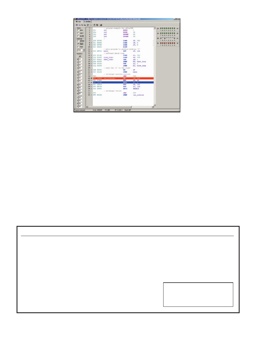
www.circuitcellar.com
CIRCUIT CELLAR
®
Issue 160 November 2003
79
Otherwise, the instruction
set is blessedly simple and
literally can be understood
at a glance (see Table 2).
Actually, even that figure
overstates the matter,
because the arithmetic and
logic group instructions are
shown twice for variants
that only differ in using a
register or constant for one
of the operands. Similarly,
the conditional JUMP,
CALL, and RETURN
instructions are shown for
each condition. By my
count, it’s really only a cou-
ple dozen instructions to
remember. Notice that
branch addresses are
absolute (i.e., constants), so
leave your computed GOTOs at home.
There is provision for a single inter-
rupt input; it just stacks the program
counter and flags, and then vectors to
a fixed (the last) location in memory
where you put a branch instruction to
the interrupt service routine. Yes, it’s
simple minded, but it’s also fast—just
a few clock cycles from interrupt
request to servicing. If you need mul-
tiple inputs, programmable priority
schemes, and so forth, remember that
this is an FPGA, so you can have it
your way by adding logic external to
the processor. Just make sure to keep
track of your stack, though—there’s
no overflow detection.
What is PicoBlaze good for? Well, as
the original programmable state
machine moniker indicates, it would
be useful for complex state machines
(e.g., recursion) that aren’t easily han-
dled by raw gates. At only two clocks
per instruction (every instruction in
all cases, thank you), you’re looking at
perhaps 40 to 60 MIPS and beyond,
depending on the particular FPGA.
By virtue of being on-chip, the core
is uniquely able to access the FPGA
internal logic and I/O pins, making it
a natural for adding self-test features,
possibly eliminating the need for an
extra processor along with the FPGA
resources (gates, pins) required to
connect it. Similarly,
PicoBlaze could provide the
basis for an externally
accessible field-test capa-
bility. For instance, by
adding a soft UART, it’s
possible to craft a scheme
by which a connected PC
could download and exe-
cute various chip-, board-,
and box-level diagnostic pro-
grams. Because a PicoBlaze
core only consumes a small
fraction of the FPGA
resources (e.g., less than 5%
of an XC3S200), it’s even fea-
sible to consider using multi-
ple cores for tackling larger
tasks or to implement a vari-
ety of useful coprocessors.
YEAH, BUT…
On the software side, there’s a full
C/C++ compiler, Java virtual machine,
and RTOS including TCP/IP stack.
Rumor has it a port of Linux is in the
works. Ha, just checking to see who’s
still awake out there. If you didn’t
immediately choke on the aforemen-
tioned statement, you’re probably
reading the wrong magazine.
The fact is, what you can download
from the Xilinx web site is a simple-
minded assembler with bare-bones
features running in a DOS window no
less. There’s also a more modern
graphical assembler/simulator from an
outfit called Mediatronix (see Photo 1),
Photo 1—The friendly assembler/simulator from Mediatronix is a quick and easy
way to get a feel for PicoBlaze programming.
Program control group
Arithmetic group
Logical group
Shift and rotate group
Interrupt group
Storage group
Input/output group
JUMP aaa
ADD sX, kk
LOAD sX, kk
SR0 sX
RETURNI ENABLE
STORE sX, ss
INPUT sX, pp
JUMP Z, aaa
ADDCY sX, kk
AND sX, kk
SR1 sX
RETURNI DISABLE
STORE sX, (sY)
INPUT sX, (sY)
JUMP NZ, aaa
SUB sX, kk
OR sX, kk
SRX sX
JUMP C, aaa
SUBCY sX, kk
XOR sX, kk
SRA sX
ENABLE INTERRUPT
FETCH sX, ss
OUTPUT sX, pp
JUMP NC, aaa
COMPARE sX, kk
TEST sX, kk
RR sX
DISABLE INTERRUT
FETCH sX, (sY)
OUTPUT sX, (sY)
CALL aaa
ADD sX, sY
LOAD sX, sY
SL0 sX
CALL Z, aaa
ADDCY sX, sY
AND sX, sY
SL1 sX
CALL NZ, aaa
SUB sX, sY
OR sX, sY
SLX sX
CALL C, aaa
SUBCY sX, sY
XOR sX, sY
SLA sX
CALL NC, aaa
COMPARE sX, sY
TEST sX, sY
RL sX
RETURN
RETURN Z
RETURN NZ
RETURN C
RETURN NC
Table 2—PicoBlaze’s blessedly simple instruction set is a welcome relief from the creeping complexity of bloatware architectures. Note that CALL and RETURN support up to
a stack depth of 31.
X and Y—register numbers in the 0–Fh range
kk—constant value in the 00–FFh range
aaa—address in the 000–3FFh range
pp—port address in the 00–FFh range
ss—internal storage address in the 00–3Fh range
80
Issue 160 November 2003
CIRCUIT CELLAR
®
www.circuitcellar.com
although in terms of credentials (i.e.,
QA, compatibility, and documentation),
there’s no guarantee you’ll get more than
what you pay for with this freeware.
Simple tools for a simple processor,
what’s wrong with that? Nothing at
all. But even though the architecture
and software tools are blessedly sim-
ple, just remember PicoBlaze ulti-
mately inherits the complexity of the
entire FPGA toolchain in all its glory.
Sure, with little more than the
PicoBlaze application note (40 pages)
and assembler (84 KB), you’re ready to
write your first Hello World program.
No problem on the hardware side
either because there are plenty of cute
and thrifty Spartan and Virtex EV
boards to choose from (see Photo 2).
But if you’re an FPGA newbie, plan
on spending plenty of time getting up
to speed. As I described earlier,
FPGAs have a bit of their own NRE
crisis, as in the nonrecurring educa-
tion crisis needed to get beyond the
“Getting Started” guide.
Even with all the chips, tools, and
know-how in hand, things are a little
cumbersome. For instance, the small
(256 × 16 or 1024 × 18) ROM your
PicoBlaze program resides in is actual-
ly a block RAM, the initialized con-
tents described somewhere in the mil-
lions of configuration bits that are
bootstrapped into the FPGA at power-
up. Thus, even the tiniest PicoBlaze
Listing 1—By overtly specifying structure (e.g., specific LUTs and flip-flops), the VHDL code for PicoBlaze
favors speed and gate count over readability.
--
Architecture low_level_definition of shift_rotate_process is
--
-- Attribute to define LUT contents during implementation
-- The information is repeated in the generic map for functional
simulation
attribute INIT : string;
attribute INIT of high_mux_lut
: label is "E4";
attribute INIT of low_mux_lut
: label is "E4";
attribute INIT of carry_out_mux_lut
: label is "E4";
--
-- Internal signals
--
signal upper_selection : std_logic;
signal lower_selection : std_logic;
signal mux_output : std_logic_vector(7 downto 0);
signal shift_in_bit : std_logic;
signal carry_bit : std_logic;
--
begin
--
-- 4 to 1 mux selection of the bit to be shifted in
--
high_mux_lut: LUT3
--translate_off
generic map (INIT => X"E4")
--translate_on
port map( I0 => code0,
I1 => operand(0),
I2 => inject_bit,
O => upper_selection );
low_mux_lut: LUT3
--translate_off
generic map (INIT => X"E4")
--translate_on
port map( I0 => code0,
I1 => carry_in,
I2 => operand(7),
O => lower_selection );
final_mux: MUXF5
port map( I1 => upper_selection,
I0 => lower_selection,
S => code1,
O => shift_in_bit );
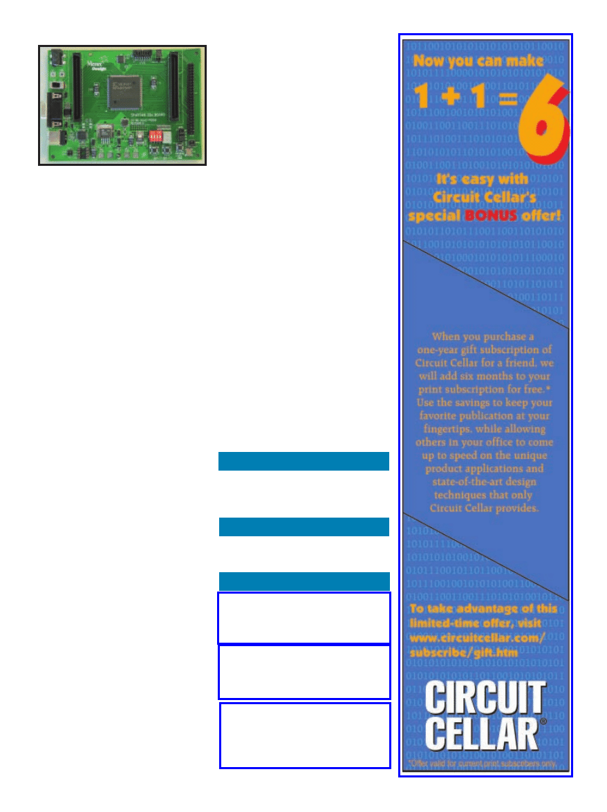
program change calls for rebuilding
the entire design and downloading a
new configuration bitstream.
An easier way out is to simply
devote another PicoBlaze core to act
as a monitor. As shown in Figure 2,
the extra core talks to a PC (or what-
ever) via UART and implements a few
commands to read/write an attached
dual-ported block RAM, which can
then be used as downloadable ROM
for the second PicoBlaze under test.
Let’s raise a glass to our dear and
departed schematics, because it looks
like HDL and synthesis are taking over.
Just out of curiosity, I glanced through
the VHDL for the PicoBlaze core. Given
the touted high-level attributes of syn-
thesis and the simplicity of the core,
you might expect the code to be rather
short and sweet. Instead, you’ll find it’s
nearly 50 pages of rather cryptic stuff
like the snippets shown in Listing 1.
It’s not the designer’s fault but
rather a case of the tool wagging the
chip. A VHDL version is a must in
order for PicoBlaze to make the most
of the toolchain (e.g., simulation). But,
at the same time, the gate bloat and
performance hit (clock rate reduction)
associated with a more behavioral
(i.e., readable) description isn’t desir-
able. Thus, the PicoBlaze VHDL codi-
fies an extremely structural definition
that tells the synthesizer explicitly
which gates go where. Kind of like
feeding a C compiler a bunch of in-
line assembly language, I guess.
DON’T BE CRUEL
Make no mistake: outfits like Xilinx
and Altera know what they’re doing. If
I were in their shoes, I’d probably fol-
low much the same strategy. Talk is
www.circuitcellar.com
CIRCUIT CELLAR
®
Issue 160 November 2003
81
REFERENCES
[1] K. Chapman, “Dynamic
Microcontroller Using XC4000
FPGAs,” Xilinx, 1994.
cheap, especially when compared to
the triple- and even quadruple-digit
prices FPGA suppliers are able to com-
mand for their highest-end parts.
For an accomplished ASIC designer
or folks who already have a lot of
FPGA experience, the complexity of
the parts and tools is less of a barrier.
They have been there, done that. But
I’m thinking there will come a time
when the ASIC suppliers are driven
back into the highest-volume niches
and the FPGA suppliers will also rec-
ognize there’s a huge potential
demand for simple parts and simpler
tools. Or maybe they’ll notice the
efforts of companies like Triscend and
Cypress Micro who are bringing pro-
grammable logic capability to design-
ers who aren’t, and shouldn’t have to
be, chip design experts.
So, if I seem overly harsh when I
grouse about the high-end, ASIC-replace-
ment orientation of FPGAs, just consider
it an example of that old saying, “You
only hurt the ones you love.”
I
SOURCES
Spartan-3 LC 50J FPGA Evaluation
kit
Insight Memec
www.insight-electronics.com
PicoBlaze Assembler/simulator
Mediatronix
+31 235625449
www.mediatronix.com
Spartan-3 FPGA, PicoBlaze 8-bit
Soft-core CPU
Xilinx, Inc.
(408) 559-7778
www.xilinx.com
Photo 2—When it comes to evaluating Spartan-3
FPGAs, hardware is the least of your worries thanks to
this low-cost ($150) evaluation board from Insight Memec.
Tom Cantrell has been working on
chip, board, and systems design and
marketing for several years. You may
reach him by e-mail at
tom.cantrell@circuitcellar.com.
RESOURCE
Xilinx, Inc., “Embedded System
Tools Guide,” V.3.2.2, May 2003.
www.circuitcellar.com
CIRCUIT CELLAR
®
Issue 160 November 2003
83
IDEA BOX
THE
DIRECTORY
OF
PRODUCTS AND
SERVICES
AD FORMAT
: Advertisers must furnish digital submission sheet and digital files that meet the specifications on the digital submission sheet.
ALL TEXT AND OTHER ELEMENTS MUST FIT WITHIN A 2
″″ ××
3
″″
FORMAT
. Call for current rate and deadline information. Send your disk and digital submis-
sion sheet to: IDEA BOX, Circuit Cellar, 4 Park Street, Vernon, CT 06066 or e-mail kc@circuitcellar.com. For more information call Sean Donnelly at (860) 872-3064.
Suppliers Directory now available online. Check out our web site
www.circuitcellar.com to see who has what and how to get it!
Insert-ready Single Board Computer modules in sub-miniature
dimensions (as small as 47x55 mm) populated by:
applicable controller signals extend to standard pin header (2.54
mm) or high-density Molex (0.625 mm) connectors, enabling SBC
to be plugged like a big chip into OEM targets
achieved via GND circuitry, multi-layer PCB, by-
pass capacitor grid and short signal traces achieved via small
footprint and use of 0402 SMD passive components
32 KB to 64 MB external SRAM and Flash (controller-dependent)
CAN, Ethernet, RS-232 and RS-485 interfaces; ADC, DAC
(controller-dependent); freely-available /CS and I/O lines
AC adapter, serial cable and SPECTRUM CD with eval software
tools, electronic documentation and demos
: insert-ready PHYTEC SBC modules accompany you
from evaluation through protyping to end production...
accelerating your design cycle and reducing your time-to-market
New Generation
Single Board Computer
Bainbridge Island, WA 98110 USA

84
Issue 160 November 2003
CIRCUIT CELLAR
®
www.circuitcellar.com
www.circuitcellar.com
CIRCUIT CELLAR
®
Issue 160 November 2003
85
Interface Keypads, Switches, or RS-232 to your PC Keyboard Input
Up to 12 x 12 matrix Programmable RS-232 Port Macro Capability
The KE24 is the ultimate in flexibility. Inputs or serial data can
emulate any of the 101 keys from a standard keyboard.
Up to 9 x 9 matrix 2.5" x 3.0" Size PC Keyboard Port PCXT, AT Compatible
The KE18 combines a multitude of features with small size at an
economical price. Custom units available.

86
Issue 160 November 2003
CIRCUIT CELLAR
®
www.circuitcellar.com
Ready-Made Graphical User Interface
Bright, High Contrast 1/4 VGA (320x240 pixel)
Electroluminescent (EL) or Monochrome Display
Precoded menu managing software
Real-time Multitasking Executive
tel: 510-790-1255 fax: 510-790-0925
applications - wherever you need an I/O rich computer and

www.circuitcellar.com
CIRCUIT CELLAR
®
Issue 160 November 2003
87

88
Issue 160 November 2003
CIRCUIT CELLAR
®
www.circuitcellar.com
sales@sealevel.com 864.843.4343
• Supports data rates up to 921K bps
www.circuitcellar.com
CIRCUIT CELLAR
®
Issue 160 November 2003
89

90
Issue 160 November 2003
CIRCUIT CELLAR
®
www.circuitcellar.com

www.circuitcellar.com
CIRCUIT CELLAR
®
Issue 160 November 2003
91

92
Issue 160 November 2003
CIRCUIT CELLAR
®
www.circuitcellar.com

www.circuitcellar.com
CIRCUIT CELLAR
®
Issue 160 November 2003
93

94
Issue 160 November 2003
CIRCUIT CELLAR
®
www.circuitcellar.com
i
Generate Video Using Software Thread Integration
The PICAVRP: A Unique Programming Solution
Low-Cost Serial LCD: Convert a Discount LCD into a Serial ASCII Display
Computer Graphics 101
TV Oscilloscope
I Above the Ground Plane: Multiplying, Dividing, and Filtering
I Applied PCs: Easing into eZ80Acclaim! Applications
I From the Bench: Tabletop DMX Control
I Silicon Update: Spin Control
84
Abacom Technologies
86
Acacetus
91
ActiveWire, Inc.
10
Adcon Telemetry
19
AeroComm, Inc.
78
All Electronics Corp.
91
Amaranthine LLC
93
Amazon Electronics
85
Animated Lighting, L.C.
84
AP Circuits
9
Arcom
7
Atmel
49
AutoTRAX
85
Avocet Systems, Inc.
84
Bagotronix, Inc.
90
Basic Micro
91
Bellin Dynamic Systems, Inc.
84
BMT Microelectronics Center
66
CadSoft Computer, Inc.
88
Capitol Automation
87
Carl’s Electronics
59
CCS-Custom Computer Services
92
Conitec
37
Connecticut microComputer, Inc.
83
Cyberpak Co.
39
Cygnal Integrated Products
1
Cypress MicroSystems
89
CWAV
91
DataRescue
83
Decade Engineering
89
Delcom Engineering
The Index of Advertisers with links to their web sites is located at www.circuitcellar.com under the current issue.
Page
73
DesignCon 2004
59
DLP Design
11
Dynon Instruments, Inc.
91
Easy Radio USA
12
Earth Computer Technologies
87
EE Tools
(Electronic Engineering Tools)
36
EMAC, Inc.
93
Embedded Micro Software
88
eProtos
69
ESEC Tokyo
10
ExpressPCB
83
FDI-Future Designs, Inc.
92
Front Panel Express
92
Futurlec
85
Hagstrom Electronics
55
HI-TECH Software, LLC
13
ICOP Technology Inc.
89
IMAGEcraft
84
Intec Automation, Inc
84
Intrepid Control Systems
91
Intronics, Inc.
33
Jameco
32, 86
JK microsystems, Inc.
85
JPA Consulting
80
JR Kerr Automation & Engineering
80
LabJack Corp.
80
Lakeview Research
47
Lemos International
2
Link Instruments
52
Linx Technologies
88
Machine Bus Corp.
50
MaxStream
90
MCC (Micro Computer Control)
53
Microchip
92
microEngineering Labs, Inc.
82
Micromint
90
MJS Consulting
86
Mosaic Industries, Inc.
88
Mouser Electronics
42
MVS
86
Mylydia Inc.
C2
NetBurner
88
OKW Electronics, Inc.
53
On Time
92
Ontrak Control Systems
40
PCB123
73
PCBexpress
87
PCB Fab Express
C4
Parallax, Inc.
83
Phytec America LLC
87
Phyton, Inc.
84
Picofab Inc.
93
Pioneer Hill Software
86
PrintCapture
93
Pulsar, Inc.
48
R2 Controls
18
R4 Systems Inc.
21
Rabbit Semiconductor
40
Remote Processing
5,63
Renesas Technology Corp.
17
Renesas Contest
90
RLC Enterprises, Inc.
Page
Page
Page
75
Saelig Company
3
Scott Edwards Electronics Inc.
90
Scidyne
88
Sealevel Systems
86
Senix Corp.
95
Sierra Proto Express
83
Signum Systems
85
Softools
84
TAL Technologies
C3
Tech Tools
89
Techniprise
26, 27
Technologic Systems
90
Technological Arts
89
Tern Inc.
89
Texas Embedded Solutions
86
TLData Corp.
85
Trace Systems, Inc.
91
Triangle Research Int’l, Inc.
37
Trilogy Design
93
Weeder Technologies
93
Xeltek
87
Z-World
86
Zagros Robotics
91
Zanthic Technologies Inc.
86
Zexus
41
Zilog, Inc
January Issue 162
Deadlines
Space Close: Nov. 10
Material Due Date: Nov. 18
Theme:
Analog Techniques
A
TTENTION
A
DVERTISERS
e-mail: sean@circuitcellar.com
Preview of December Issue 161
Theme: Graphics & Video
INDEX OF ADVERTISERS
Their boards come with a
packing slip. Ours come
with a
Microsection
Analysis Report
In today’s competitive climate, offering the
best product at a competitive price is a must
to satisfy your customers. Sierra Proto
Express offers the fastest, most reliable, turns
at the highest quality. And we’ll prove it in
every shipment with our unique Evidence of
Quality reports, so you know your board is
right the first time. One proof of quality is
our Microsection Analysis Report, as
featured here, so you can see the quality
inside your board. And that is just part of
our comprehensive quality tests. It’s in our
process, not in our price. In fact, it is our
commitment to total quality that enables us
to run our operation cost effectively. And
that comes back to you in our competitive
price. Talk to a Sierra Proto Express Account
Manager about our commitment to quality,
our range of technology, and our 99%
on-time track record of delivery. Call
1.800.763.7503 from 6 a.m. to 6 p.m. PST
or email your design to
files@protoexpress.com and receive a quote.
Mention code: PPDC00093
For proven quality that never costs
extra, put Sierra Proto Express on
your team today.
14 Layer Board
Microsection
Learn more about our unique Evidence of
Quality report that comes with every PCB
at www.protoexpress.com

I
recently read an interesting observation. It said that all the spam attacks lately are good for the Internet because it spurs business growth
in anti-spam technology and keeps everyone on a system upgrade path that is ultimately good for both hardware and software manufactur-
ers. When I read warped logic like this, I cannot help but think of the same lame trickle-down argument from Indian gambling lobbyists who
think that because casinos employ lots of people they shouldnt have to pay taxes. But dont get me started on that.
Spam and virus attacks are an outrageous nuisance that without remedial intervention could ultimately deep-six one of the few remaining
free-enterprise zones on the planet. The growth of the Internet has been driven by commerce and communication. These days, could you real-
ly live without e-mail or the ability to get your hands on vast quantities of information on virtually any subject with the click of a key? The future
vitality of the Internet depends on the unfettered interaction of legitimate users and sources, both commercial and private.
How anxious are you to continue ordering products online when you have to worry that your credit card number might be hacked by someone
sitting in the same Wi-Fi-enabled coffee shop or, worse yet, that you actually entered all of your credit information in a fraudulent phisher site
that exactly mimics a legitimate e-commerce site? Antivirus utilities and spam filters attack only part of the problem these days.
Statistics suggest that 30% of the e-mail on the Internet is spam, up from 10% a couple of years ago. I cannot speak for you, but fully 95%
of my e-mail is spam. That is, unless it is the result of some virus attack and it goes even higher. I remember a recent two-day span when all
we saw around our place were piles of incoming e-mail with 100K attachments clogging the system. The combination of spam, viruses, and
outright fraud are making the Internet a very inhospitable placea situation that will surely stunt its continued growth.
One argument is to blame it on Microsoft, but it is naive and unfair to simply blame the situation on the failings of Microsoft products, espe-
cially Outlook. The predominance of Windows and Outlook is a de facto state of affairs brought on by the rapid evolution of the Internet. Outlook
gets hacked because it is there. If we all switched to Linux and another e-mail program, it would merely become the new target. At least
Microsoft has enough resources to plug the holes when they arise. Many other companies would not.
The latest hall of Internet infamy is something called browser spam, which pops up random advertisements as you are surfing the Net.
Slipped into your computer with spyware or freeware programs, the program silently watches where you surf. When you land on a site con-
taining keywords, it pops up ads intended to divert you to the spammers site. It sounded fearfully familiar to me when I heard about it, and I
remember experiencing something even worse. I remember accidentally clicking on something once that replaced my browser home page
designation, stuffed a dozen very offensive web sites into my Favorites list, and disabled my ability to erase cookies. I had to reload the entire
computer to clear out all the crud.
Were at a critical point where we have to decide who will control the Internet. I dont want the alternatives to be the government or none.
To regain control of the Internet, every legitimate constituency that uses it will have to bear some responsibility for maintaining its integrity.
Corporations from the size of IBM down to little guys like Circuit Cellar will have to recognize that there is a certain expense involved in main-
taining Net security with the proper firewall software. Having a computer system that can be easily hacked so that it becomes a focal point of
virus proliferation should not be allowed. The government will have to make the Net safe for businesses by truly cracking down on spammers
and con men. If sending a porn spam message to someone under 14 in the U.S. is a felony, then put them in jail.
Finally, Internet users have to become savvier. Phisher sites wouldnt proliferate if people were smart enough not to respond to stupid e-
mails asking them to enter their complete financial details on a phony web site for no other reason than being asked. Net users need to be
educated that there are some really nasty things that they have to be aware of when they go online and then actually have it sink in. Only by
all of us maintaining an adequate level of system defense at every stage along with a workable strategy for validating interactive communica-
tion can we ever hope to counteract the con men, spammers, and hackers. It shouldnt be left to the government alone.
Internet Infamy
steve.ciarcia@circuitcellar.com
96
Issue 160 November 2003
CIRCUIT CELLAR
®
www.circuitcellar.com
by Steve Ciarcia, Founder and Editorial Director
PRIORITY INTERRUPT

Wyszukiwarka
Podobne podstrony:
circuit cellar1996 11
circuit cellar1993 11
circuit cellar1994 11
circuit cellar1997 11
circuit cellar2004 11
circuit cellar2000 11
circuit cellar1995 11
circuit cellar2002 11
circuit cellar2001 11
circuit cellar2003 11
circuit cellar1996 11
circuit cellar1993 11
circuit cellar1995 11
circuit cellar1996 11
circuit cellar1997 11
circuit cellar1993 11
więcej podobnych podstron
