Philips Semiconductors
Product specification
NE/SA/SE532/
LM158/258/358/A/2904
Low power dual operational amplifiers
1
1995 Nov 27
853-1241 16050
DESCRIPTION
The 532/358/LM2904 consists of two independent, high gain,
internally frequency-compensated operational amplifiers internally
frequency-compensated operational amplifiers designed specifically
to operate from a single power supply over a wide range of voltages.
Operation from dual power supplies is also possible, and the low
power supply current drain is independent of the magnitude of the
power supply voltage.
UNIQUE FEATURES
In the linear mode the input common-mode voltage range includes
ground and the output voltage can also swing to includes ground
and the output voltage can also swing to ground, even though
operated from only a single power supply voltage. The unity gain
cross frequency is temperature-compensated. The input bias current
is also temperature-compensated.
FEATURES
•
Internally frequency-compensated for unity gain
•
Large DC voltage gain—100dB
•
Wide bandwidth (unity gain)—1MHz (temperature-compensated)
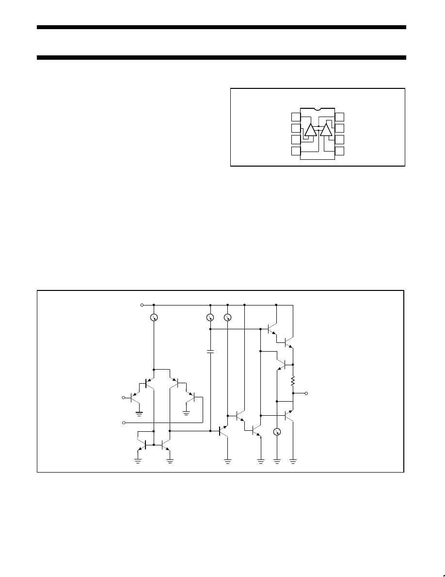
PIN CONFIGURATIONS
1
2
3
4
5
6
7
8
– +
+ –
A
B
V+
OUTPUT B
INVERTING INPUT B
NON INVERTING INPUT B
OUTPUT A
INVERTING INPUT A
NON INVERTING INPUT A
V–
D, FE, N Packages
SL00282
Figure 1. Pin Configuration
•
Wide power supply range single supply—3V
DC
to 30V
DC
or dual
supplies—
±
1.5V
DC
to
±
15V
DC
•
Very low supply current drain (400
µ
A)—essentially independent of
supply voltage (1mW/op amp at +5V
DC
)
•
Low input biasing current—45nA
DC
temperature-compensated
•
Low input offset voltage—2mV
DC
and offset current—5nA
DC
•
Differential input voltage range equal to the power supply voltage
•
Large output voltage—0V
DC
to V+ 1.5V
DC
swing
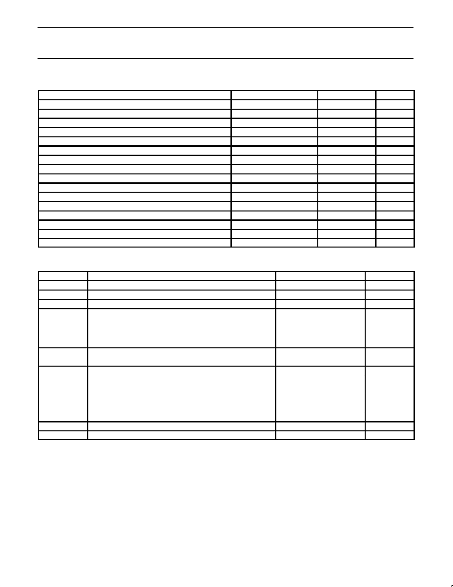
EQUIVALENT CIRCUIT
v+
6
µ
A
100
µ
A
Q2
Q3
Q1
Q4
INPUTS
+
Q8
Q9
CC
Q10
6
µ
A
Q5
Q7
Q6
RSC
OUTPUT
Q13
Q12
Q11
50
µ
A
SL00283
Figure 2. Equivalent Circuit
Philips Semiconductors
Product specification
NE/SA/SE532/
LM158/258/358/A/2904
Low power dual operational amplifiers
1995 Nov 27
2
ORDERING INFORMATION
DESCRIPTION
TEMPERATURE RANGE
ORDER CODE
DWG #
8-Pin Plastic Small Outline (SO) Package
0 to +70
°
C
NE532D
SOT96-1
8-Pin Plastic Dual In-Line Package (DIP)
0 to +70
°
C
NE532N
SOT97-1
8-Pin Plastic Small Outline (SO) Package
-40
°
C to +85
°
C
SA532D
SOT96-1
8-Pin Plastic Dual In-Line Package (DIP)
-40
°
C to +85
°
C
SA532N
SOT97-1
8-Pin Ceramic Dual In-Line Package (CERDIP)
-40
°
C to +85
°
C
SA532FE
0580A
8-Pin Plastic Small Outline (SO) Package
-40
°
C to +125
°
C
LM2904D
SOT96-1
8-Pin Plastic Dual In-Line Package (DIP)
-40
°
C to +125
°
C
LM2904N
SOT97-1
8-Pin Ceramic Dual In-Line Package (CERDIP)
-55
°
C to +125
°
C
LM158FE
0580A
8-Pin Plastic Dual In-Line Package (DIP)
-25
°
C to +125
°
C
LM258N
SOT97-1
8-Pin Plastic Small Outline (SO) Package
-25
°
C to +125
°
C
LM258D
SOT96-1
8-Pin Plastic Small Outline (SO) Package
0 to +70
°
C
LM358D
SOT96-1
8-Pin Plastic Dual In-Line Package (DIP)
0 to +70
°
C
LM358N
SOT97-1
8-Pin Plastic Dual In-Line Package (DIP)
0 to +70
°
C
LM358AN
SOT97-1
8-Pin Plastic Small Outline (SO) Package
0 to +70
°
C
LM358AD
SOT96-1
8-Pin Plastic Dual In-Line Package (DIP)
-55
°
C to +125
°
C
SE532N
SOT97-1
8-Pin Ceramic Dual In-Line Package (CERDIP)
-55
°
C to +125
°
C
SE532FE
0580A
ABSOLUTE MAXIMUM RATINGS
SYMBOL
PARAMETER
RATING
UNIT
V
S
Supply voltage, V+
32 or
±
16
V
DC
Differential input voltage
32
V
DC
V
IN
Input voltage
-0.3 to +32
V
DC
P
D
Maximum power dissipation
T
A
=25
°
C (Still air)
1
FE package
N package
D package
780
1160
780
mW
mW
mW
Output short-circuit to GND
5
V+<15 V
DC
and T
A
=25
°
C
Continuous
Operating ambient temperature range
NE532/LM358/LM358A
0 to +70
°
C
T
A
LM258
-25 to +85
°
C
LM2904
-40 to +125
°
C
SA532
-40 to +85
°
C
SE532/LM158
-55 to +125
°
C
T
STG
Storage temperature range
-65 to +150
°
C
T
SOLD
Lead soldering temperature (10sec max)
300
°
C
NOTES:
1. Derate above 25
°
C, at the following rates:
FE package at 6.2mW/
°
C
N package at 9.3mW/
°
C
D package at 6.2mW/
°
C
Philips Semiconductors
Product specification
NE/SA/SE532/
LM158/258/358/A/2904
Low power dual operational amplifiers
1995 Nov 27
3
DC ELECTRICAL CHARACTERISTICS
T
A
= 25
°
C, V+=+5V, unless otherwise specified.
SYMBOL
PARAMETER
TEST CONDITIONS
SE532, LM158/258
NE/SA532/
LM358/LM2904
UNIT
SYMBOL
PARAMETER
TEST CONDITIONS
Min
Typ
Max
Min
Typ
Max
UNIT
V
OS
Offset voltage
1
R
S
=0
Ω
R
S
=0
Ω
, over temp.
±
2
±
5
±
7
±
2
±
7
±
9
mV
mV
V
OS
Drift
R
S
=0
Ω
, over temp.
7
7
µ
V/
°
C
I
OS
Offset current
I
IN
(+)-I
IN
(-)
Over temp.
±
3
±
30
±
100
±
5
±
50
±
150
nA
nA
I
OS
Drift
Over temp.
10
10
pA/
°
C
I
BIAS
Input current
2
I
IN
(+) or I
IN
(-)
Over temp., I
IN
(+) or I
IN
(-)
45
40
150
300
45
40
250
500
nA
nA
I
B
Drift
Over temp.
50
50
pA/
°
C
V
CM
Common-mode voltage
V+=30V
0
V+-1.5
0
V+-1.5
V
range
3
Over temp., V+=30V
0
V+-2.0
0
V+-2.0
V
CMRR
Common-mode rejection
ratio
V+=30V
70
85
65
70
dB
V
OH
Output voltage swing
R
L
≥
2k
Ω
, V+=30V,
over temp.
26
26
V
R
L
≥
10k
Ω
, V+=30V,
over temp.
27
28
27
28
V
V
OL
Output voltage swing
R
L
≥
10k
Ω
, over temp.
5
20
5
20
mV
I
CC
Supply current
R
L
=
∞
, V+=30V
R
L
=
∞
on all amplifiers,
over temp., V+ =30V
0.5
0.6
1.0
1.2
0.5
0.6
1.0
1.2
mA
mA
A
VOL
Large-signal voltage gain
R
L
≥
2k
Ω
, V
OUT
±
10V,
V+=15V
(for large V
O
swing)
over temp.
50
25
100
25
15
100
V/mV
V/mV
PSRR
Supply voltage rejection
ratio
R
S
=0
Ω
65
100
65
100
dB
Amplifier-to-amplifier cou-
pling
4
f=1kHz to 20kHz
(input referred)
-120
-120
dB
I
OUT
Output current
Source
V
IN+
=+1V
DC
, V
IN-
=0V
DC
,
V+=15V
DC
20
40
20
40
mA
V
IN+
=+1V
DC
, V
IN-
=0V
DC
,
V+=15V
DC
, over temp.
10
20
10
20
mA
Sink
V
IN-
=+1V
DC
, V
IN+
=0V
DC
,
V+=15V
DC
10
20
10
20
mA
V
IN-
=+1V
DC
, V
IN+
=0V
DC
,
V+=15V
DC
, over temp.
5
8
5
8
mA
V
IN+
=0V, V
IN-
=+1V
DC
,
V
O
=200mV
12
50
12
50
µ
A
I
SC
Short circuit current
5
40
60
40
60
mA
Differential input voltage
6
V+
V+
V
GBW
Unity gain bandwidth
T
A
=25
°
C
1
1
MHz
SR
Slew rate
T
A
=25
°
C
0.3
0.3
V/
µ
s
V
NOISE
Input noise voltage
T
A
=25
°
C, f=1kHz
40
40
nV/
√
Hz
Philips Semiconductors
Product specification
NE/SA/SE532/
LM158/258/358/A/2904
Low power dual operational amplifiers
1995 Nov 27
4
DC ELECTRICAL CHARACTERISTICS
T
A
=25
°
C, V+=+5V, unless otherwise specified.
SYMBOL
PARAMETER
TEST CONDITIONS
LM358A
UNIT
SYMBOL
PARAMETER
TEST CONDITIONS
Min
Typ
Max
UNIT
V
OS
Offset voltage
1
R
S
=0
Ω
R
S
=0
Ω
, over temp.
±
2
±
3
±
5
mV
mV
V
OS
Drift
R
S
=0
Ω
, over temp.
7
20
µ
V/
°
C
I
OS
Offset current
I
IN
(+)-I
IN
(-)
Over temp.
5
±
30
±
75
nA
nA
I
OS
Drift
Over temp.
10
300
pA/
°
C
I
BIAS
Input current
2
I
IN
(+) or I
IN
(-)
Over temp., I
IN
(+) or I
IN
(-)
45
40
100
200
nA
nA
I
B
Drift
Over temp.
50
pA/
°
C
V
CM
Common-mode voltage
V+=30V
0
V+-1.5
V
range
3
Over temp., V+=30V
0
V+-2.0
V
CMRR
Common-mode rejection ratio
V+=30V
65
85
dB
V
OH
Output voltage swing
R
L
≥
2k
Ω
, V+=30V,
over temp.
26
V
R
L
≥
10k
Ω
, V+=30V,
over temp.
27
28
V
V
OL
Output voltage swing
R
L
≥
10k
Ω
, over temp.
5
20
mV
I
CC
Supply current
R
L
=
∞
, V+=30V
R
L
=
∞
on all amplifiers,
over temp., V+ =30V
0.5
0.6
1.0
1.2
mA
mA
A
VOL
Large-signal voltage gain
R
L
≥
2k
Ω
, V
OUT
±
10V,
V+=15V
(for large V
O
swing)
over temp.
25
15
100
V/mV
V/mV
PSRR
Supply voltage rejection ratio
R
S
=0
Ω
65
100
dB
Amplifier-to-amplifier coupling
4
f=1kHz to 20kHz (input referred)
-120
dB
I
OUT
Output current
Source
V
IN+
=+1V
DC
, V
IN-
=0V
DC
,
V+=15V
DC
20
40
mA
V
IN+
=+1V
DC
, V
IN-
=0V
DC
,
V+=15V
DC
, over temp.
10
20
mA
Sink
V
IN-
=+1V
DC
, V
IN+
=0V
DC
,
V+=15V
DC
10
20
mA
V
IN-
=+1V
DC
, V
IN+
=0V
DC
,
V+=15V
DC
, over temp.
5
8
mA
V
IN+
=0V, V
IN-
=+1V
DC
,
V
O
=200mV
12
50
µ
A
I
SC
Short circuit current
5
40
60
mA
Differential input voltage
6
V+
V
GBW
Unity gain bandwidth
T
A
=25
°
C
1
MHz
SR
Slew rate
T
A
=25
°
C
0.3
V/
µ
s
V
NOISE
Input noise voltage
T
A
=25
°
C, f=1kHz
40
nV/
√
Hz
NOTES:
1. V
O
≈
1.4V, R
S
=0
Ω
with V+ from 5V to 30V; and over the full input common-mode range (0V to V+ -1.5V).
2. The direction of the input current is out of the IC due to the PNP input stage. This current is essentially constant, independent of the state of
the output so no loading change exists on the input lines.
3. The input common-mode voltage or either input signal voltage should not be allowed to go negative by more than 0.3V. The upper end of the
common-mode voltage range is V+ -1.5V, but either or both inputs can go to +32V without damage.
4. Due to proximity of external components, insure that coupling is not originating via stray capacitance between these external parts. This
typically can be detected as this type of capacitance coupling increases at higher frequencies.
5. Short-circuits from the output to V+ can cause excessive heating and eventual destruction. The maximum output current is approximately
40mA independent of the magnitude of V+. At values of supply voltage in excess of +15V
DC
, continuous short-circuits can exceed the power
dissipation ratings and cause eventual destruction.
6. The input common-mode voltage or either input signal voltage should not be allowed to go negative by more than 0.3V. The upper end of the
common-mode voltage range is V+ -1.5V, but either or both inputs can go to +32V
DC
without damage.
Philips Semiconductors
Product specification
NE/SA/SE532/
LM158/258/358/A/2904
Low power dual operational amplifiers
1995 Nov 27
5
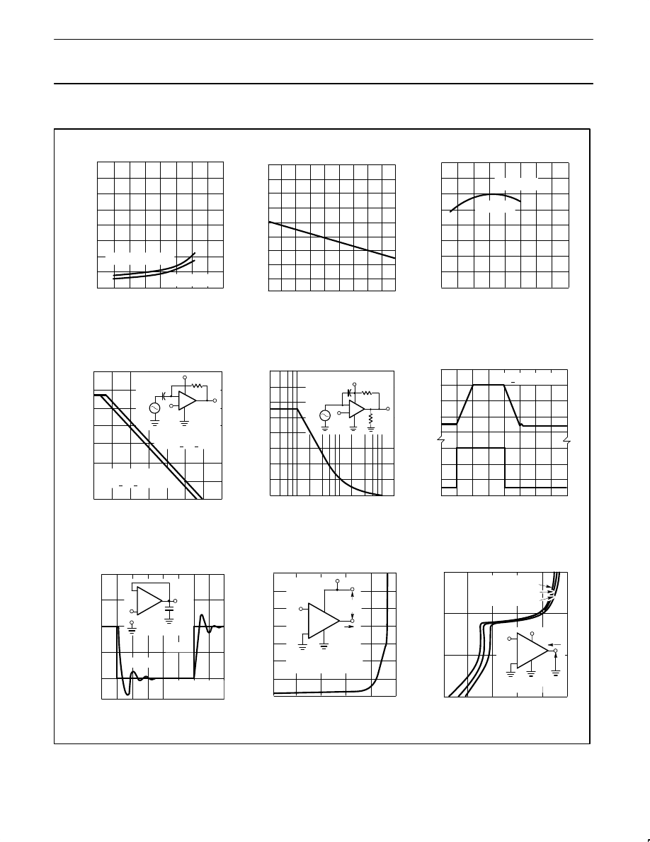
TYPICAL PERFORMANCE CHARACTERISTICS
V – OUTPUT VOL
T
AGE (V )
O
–
+
VDC
100K
VO
1K
+7
VDC
VIN
2K
TA = 0
o
C to +125
o
C
TA = 55
o
C
4
3
2
1
0
0
10
20
30
40
SUPPLY VOLTAGE (VDC)
SUPPL
Y
CURRENT DRAIN (mA
) DC
90
80
70
60
50
40
30
20
10
0
55 35 –15
5
25
45 65
85 105 125
TEMPERATURE (
o
C)
OUTPUT CURRENT (mA
) DC
160
120
80
40
0
0
10
20
30
40
SUPPLY VOLTAGE (VDC)
RL + 20 k
Ω
RL + 2 k
Ω
A
— VOL
T
AGE GAIN (dB)
VOL
–
+
V+
10M
VO
0.1
µ
f
V+/2
VIN
V+ = 30 VDC AND
–55
o
C < TA < +125
o
C
V+ = 10 to 15 VDC AND
–55
o
C < TA < +125
o
C
140
120
100
80
60
40
20
0
1
10
100
1K
10K
100K 1M 10M
FREQUENCY (Hz)
VOL
T
AGE GAIN (dB)
20
15
10
5
0
1K
10K
100K
1M
FREQUENCY (Hz)
V — OUTPUT SWING (V )
O
p–p
RL < 2K V
+ 15 VDC
4
3
2
1
0
3
2
1
0
0
10
20
30
40
TIME (
µ
S)
OUTPUT VOL
T
AGE (V)
INPOUT VOL
T
AGE (V)
EO
50pF
INPUT
OUTPUT
θ
IN
500
450
400
350
300
250
0
1
2
3
4
5
6
7
8
t — TIME (
µ
S)
TA = +25
o
C
V
+
= +30 VDC
E – OUTPUT VOL
T
AGE (mV)
O
+V+
/2
V+
V2
IO
INDEPENDENT OF V+
TA = +25
o
C
8
7
6
5
4
3
2
1
0.001
0.01
0.1
1
10
100
IO
+ – OUTPUT SOURCE CURRENT (mADC)
V – OUTPUT VOL
T
AGE
REFERENCE T
O V+ (VD )
DC
∆
V+
/2
V+
IO
TA = +25
o
C
V+ = +5 VDC
V+ = +15 VDC
V+ = +30 VDC
10
1
0.1
0.01
0.001
0.01
0.1
1
10
100
IO – OUTPUT SINK CURRENT (mADC)
DC
VO
–
+
+
–
Supply Current
Current Limiting
Voltage Gain
Open–Loop Frequency
Response
Large–Signal Frequency
Response
Voltage–Follower
Response
Voltage–Follower Pulse
Response (Small–Signal)
Output Characteristics
Current Sourcing
Output Characteristics
Current Sinking
SL00284
Figure 3. Typical Performance Characteristics
Philips Semiconductors
Product specification
NE/SA/SE532/
LM158/258/358/A/2904
Low power dual operational amplifiers
1995 Nov 27
6
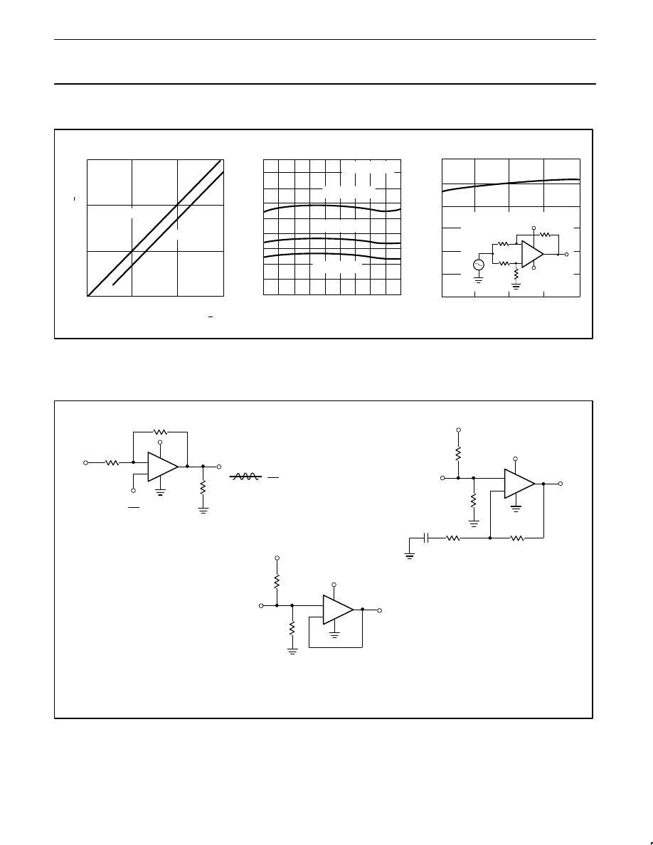
TYPICAL PERFORMANCE CHARACTERISTICS
(Continued)
+V — INPUT VOL
T
AGE ( V )
15
10
5
NEGATIVE
POSITIVE
0
5
10
15
V+ OR V– — POWER SUPPLY VOLTAGE (+ VDC)
IN
DC
+
VCM = 0 VDC
V+ = +30 VDC
V+ = +15 VDC
V+ = +5 VDC
90
80
70
60
50
40
30
20
10
0
–55 –35 –15
5
25
45
65
85 105 125
TA — TEMPERATURE (C
o
)
I – INPUT CURRENT (nA
)
B
DC
100
100
100k
7.5 VDC
VO
100k
–
+
+
VIN
+7.5 VDC
120
100
80
60
40
20
0
100
1k
10k
100k
1M
f — FREQUENCY (Hz)
CMRR — COMMON–MODE REJECTION RA
TIO (dB)
Input Voltage Range
Input Current
Common–Mode Rejection Ratio
SL00285
Figure 4. Typical Performance Characteristics (cont.)
TYPICAL APPLICATIONS
V+
2
Non-Inverting Amplifier
RF
V+
8
RL
VO
RIN
V+
2
V
I
N
–
+
4
V+
8
VO
V
I
N
–
+
4
V+
10K
10k
V+
8
VO
V
I
N
–
+
4
V+
10K
10k
RF
BLOCKS
DC.
GAIN
R1
Single Supply Inverting Amplifier
Input Biasing Voltage Follower
SL00286
Figure 5. Typical Applications
Wyszukiwarka
Podobne podstrony:
ne532
LM258 LM358 LM2904 NE532 SA532 SE532
więcej podobnych podstron