Product data
Supersedes data of 2002 Jan 22
NE/SA/SE532
LM258/358/A/2904
Low power dual operational amplifiers
2002 Jul 12
INTEGRATED CIRCUITS
Philips Semiconductors
Product data
NE/SA/SE532/
LM258/358/A/2904
Low power dual operational amplifiers
2
2002 Jul 12
853-1241 28616
DESCRIPTION
The 532/358/LM2904 consists of two independent, high gain,
internally frequency-compensated operational amplifiers internally
frequency-compensated operational amplifiers designed specifically
to operate from a single power supply over a wide range of voltages.
Operation from dual power supplies is also possible, and the low
power supply current drain is independent of the magnitude of the
power supply voltage.
UNIQUE FEATURES
In the linear mode the input common-mode voltage range includes
ground and the output voltage can also swing to includes ground
and the output voltage can also swing to ground, even though
operated from only a single power supply voltage. The unity gain
cross frequency is temperature-compensated. The input bias current
is also temperature-compensated.
FEATURES
•
Internally frequency-compensated for unity gain
•
Large DC voltage gain: 100 dB
•
Wide bandwidth (unity gain): 1 MHz (temperature-compensated)
•
Wide power supply range single supply: 3 V
DC
to 30 V
DC
,
or dual supplies:
±
1.5 V
DC
to
±
15 V
DC
•
Very low supply current drain (400
µ
A)—essentially independent
of supply voltage (1 mW/op amp at +5 V
DC
)
•
Low input biasing current: 45 nA
DC
temperature-compensated
•
Low input offset voltage: 2 mV
DC
, and offset current: 5nA
DC
•
Differential input voltage range equal to the power supply voltage
•
Large output voltage: 0 V
DC
to V+ 1.5 V
DC
swing
PIN CONFIGURATION
1
2
3
4
5
6
7
8
– +
+ –
A
B
V+
OUTPUT B
INVERTING INPUT B
NON INVERTING INPUT B
OUTPUT A
INVERTING INPUT A
NON INVERTING INPUT A
V–
D, DP, and N Packages
SL00282
Figure 1. Pin configuration.
EQUIVALENT CIRCUIT
V+
6
µ
A
100
µ
A
Q2
Q3
Q1
Q4
INPUTS
+
Q8
Q9
C
C
Q10
6
µ
A
Q5
Q7
Q6
R
SC
OUTPUT
Q13
Q12
Q11
50
µ
A
SL00283
–
Figure 2. Equivalent circuit.
Philips Semiconductors
Product data
NE/SA/SE532/
LM258/358/A/2904
Low power dual operational amplifiers
2002 Jul 12
3
ORDERING INFORMATION
DESCRIPTION
TEMPERATURE RANGE
ORDER CODE
DWG #
8-Pin Plastic Small Outline (SO) Package
0
°
C to +70
°
C
NE532D
SOT96-1
8-Pin Plastic Dual In-Line Package (DIP)
0
°
C to +70
°
C
NE532N
SOT97-1
8-Pin Plastic Small Outline (SO) Package
–40
°
C to +85
°
C
SA532D
SOT96-1
8-Pin Plastic Small Outline (SO) Package
–40
°
C to +125
°
C
LM2904D
SOT96-1
8-Pin Plastic Thin Shrink Small Outline Package (TSSOP)
–40
°
C to +125
°
C
LM2904DP
SOT505-1
8-Pin Plastic Dual In-Line Package (DIP)
–40
°
C to +125
°
C
LM2904N
SOT97-1
8-Pin Plastic Small Outline (SO) Package
–25
°
C to +125
°
C
LM258D
SOT96-1
8-Pin Plastic Dual In-Line Package (DIP)
–25
°
C to +125
°
C
LM258N
SOT97-1
8-Pin Plastic Small Outline (SO) Package
0
°
C to +70
°
C
LM358D
SOT96-1
8-Pin Plastic Thin Shrink Small Outline Package (TSSOP)
0
°
C to +70
°
C
LM358DP
SOT505-1
8-Pin Plastic Dual In-Line Package (DIP)
0
°
C to +70
°
C
LM358N
SOT97-1
8-Pin Plastic Small Outline (SO) Package
0
°
C to +70
°
C
LM358AD
SOT96-1
8-Pin Plastic Dual In-Line Package (DIP)
0
°
C to +70
°
C
LM358AN
SOT97-1
8-Pin Plastic Dual In-Line Package (DIP)
–55
°
C to +125
°
C
SE532N
SOT97-1
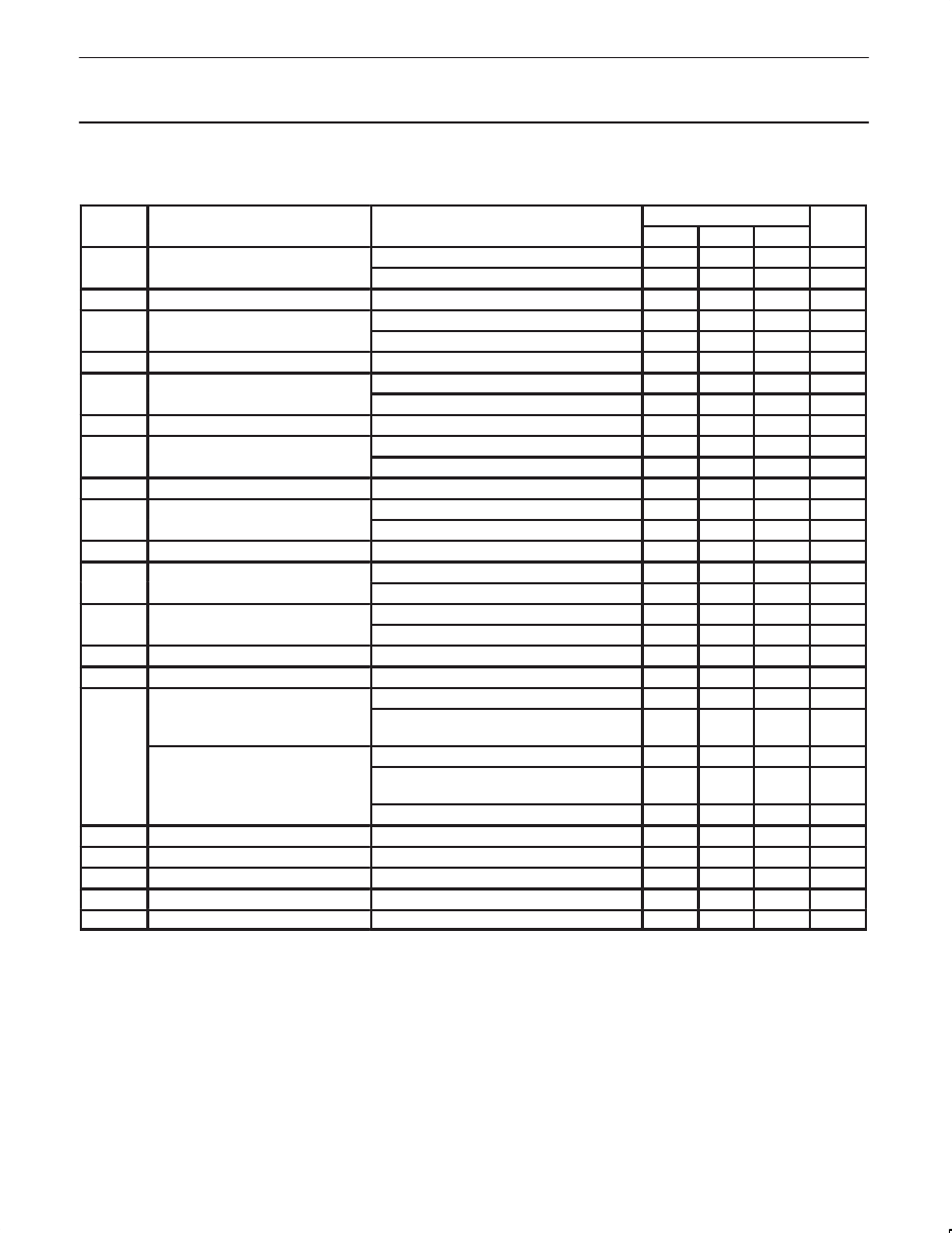
ABSOLUTE MAXIMUM RATINGS
SYMBOL
PARAMETER
RATING
UNIT
V
S
Supply voltage, V+
32 or
±
16
V
DC
Differential input voltage
32
V
DC
V
IN
Input voltage
–0.3 to +32
V
DC
Maximum power dissipation
T
amb
= 25
°
C (Still air)
1
P
D
N package
1160
mW
D package
780
mW
DP package
714
mW
Output short-circuit to GND
2
V+ < 15 V
DC
and T
amb
= 25
°
C
Continuous
Operating ambient temperature range
NE532/LM358/LM358A
0 to +70
°
C
T
amb
LM258
–25 to +85
°
C
T
amb
LM2904
–40 to +125
°
C
SA532
–40 to +85
°
C
SE532
–55 to +125
°
C
T
stg
Storage temperature range
–65 to +150
°
C
T
sld
Lead soldering temperature (10 sec max)
230
°
C
NOTE:
1. Derate above 25
°
C, at the following rates:
N package at 9.3 mW/
°
C
D package at 6.2 mW/
°
C
DP package at 5.72 mW/
°
C
2. Short-circuits from the output to V+ can cause excessive heating and eventual destruction. The maximum output current is approximately
40 mA independent of the magnitude of V+. At values of supply voltage in excess of +15 V
DC
, continuous short-circuits can exceed the
power dissipation ratings and cause eventual destruction.
Philips Semiconductors
Product data
NE/SA/SE532/
LM258/358/A/2904
Low power dual operational amplifiers
2002 Jul 12
4
DC ELECTRICAL CHARACTERISTICS
T
amb
= 25
°
C; V+ = +5 V, unless otherwise specified.
SYMBOL
PARAMETER
TEST CONDITIONS
SE532, LM258
NE/SA532/
LM358/LM2904
UNIT
Min
Typ
Max
Min
Typ
Max
V
OS
Offset voltage
1
R
S
= 0
Ω
±
2
±
5
±
2
±
7
mV
V
OS
Offset voltage
1
R
S
= 0
Ω
; over temp.
±
7
±
9
mV
V
OS
Drift
R
S
= 0
Ω
; over temp.
7
7
µ
V/
°
C
I
OS
Offset current
I
IN(+)
– I
IN(–)
±
3
±
30
±
5
±
50
nA
I
OS
Offset current
Over temp.
±
100
±
150
nA
I
OS
Drift
Over temp.
10
10
pA/
°
C
I
S
Input current
2
I
IN(+)
or I
IN(–)
45
150
45
250
nA
I
BIAS
Input current
2
I
IN(+)
or I
IN(–)
; Over temp.
40
300
40
500
nA
I
B
Drift
Over temp.
50
50
pA/
°
C
V
C
Common-mode voltage
V+ = 30 V
0
V+–1.5
0
V+–1.5
V
V
CM
g
range
3
V+ = 30 V; Over temp.
0
V+–2.0
0
V+–2.0
V
CMRR
Common-mode rejection
ratio
V+ = 30 V
70
85
65
70
dB
V
O
Output voltage swing
R
L
≥
2 k
Ω
; V+ = 30 V; over temp.
26
26
V
V
OH
Output voltage swing
R
L
≥
10 k
Ω
; V+ = 30 V; over temp.
27
28
27
28
V
V
OL
Output voltage swing
R
L
≥
10 k
Ω
; over temp.
5
20
5
20
mV
R
L
=
∞
; V+ = 30 V
0.5
1.0
0.5
1.0
mA
I
CC
Supply current
R
L
=
∞
on all amplifiers; V+ = 30 V;
over temp.
0.6
1.2
0.6
1.2
mA
R
L
≥
2 k
Ω
; V
OUT
±
10 V
50
100
25
100
V/mV
A
VOL
Large-signal voltage gain
V+=15V (for large V
O
swing);
over temp.
25
15
V/mV
PSRR
Supply voltage rejection
ratio
R
S
= 0
Ω
65
100
65
100
dB
Amplifier-to-amplifier
coupling
4
f = 1 kHz to 20 kHz (input referred)
–120
–120
dB
Output current (Source)
V
IN+
= +1 V
DC
; V
IN–
= 0 V
DC
;
V+ = 15 V
DC
20
40
20
40
mA
Output current (Source)
V
IN+
= +1 V
DC
; V
IN–
= 0 V
DC
;
V+ = 15 V
DC
; over temp.
10
20
10
20
mA
I
OUT
V
IN–
= +1 V
DC
; V
IN+
= 0 V
DC
;
V+ = 15 V
DC
10
20
10
20
mA
Output current (Sink)
V
IN–
= +1 V
DC
; V
IN+
= 0 V
DC
;
V+ = 15 V
DC
; over temp.
5
8
5
8
mA
V
IN+
= 0 V; V
IN–
= +1 V
DC
;
V
O
= 200 mV
12
50
12
50
µ
A
I
SC
Short circuit current
5
40
60
40
60
mA
Differential input voltage
6
V+
V+
V
GBW
Unity gain bandwidth
T
amb
= 25
°
C
1
1
MHz
SR
Slew rate
T
amb
= 25
°
C
0.3
0.3
V/
µ
s
V
NOISE
Input noise voltage
T
amb
= 25
°
C; f = 1 kHz
40
40
nV/
√
Hz
(Notes on next page).
Philips Semiconductors
Product data
NE/SA/SE532/
LM258/358/A/2904
Low power dual operational amplifiers
2002 Jul 12
5
DC ELECTRICAL CHARACTERISTICS (continued)
T
amb
= 25
°
C; V+ = +5 V; unless otherwise specified.
SYMBOL
PARAMETER
TEST CONDITIONS
LM358A
UNIT
SYMBOL
PARAMETER
TEST CONDITIONS
Min
Typ
Max
UNIT
V
OS
Offset voltage
1
R
S
= 0
Ω
±
2
±
3
mV
V
OS
Offset voltage
1
R
S
= 0
Ω
; over temp.
±
5
mV
V
OS
Drift
R
S
= 0
Ω
; over temp.
7
20
µ
V/
°
C
I
OS
Offset current
I
IN(+)
– I
IN(–)
5
±
30
nA
I
OS
Offset current
Over temp.
±
75
nA
I
OS
Drift
Over temp.
10
300
pA/
°
C
I
S
Input current
2
I
IN(+)
or I
IN(–)
45
100
nA
I
BIAS
Input current
2
I
IN(+)
or I
IN(–)
; Over temp.
40
200
nA
I
B
Drift
Over temp.
50
pA/
°
C
V
C
Common mode voltage range
3
V+ = 30 V
0
V+–1.5
V
V
CM
Common-mode voltage range
3
V+ = 30 V; Over temp.
0
V+–2.0
V
CMRR
Common-mode rejection ratio
V+ = 30 V
65
85
dB
V
O
Output voltage swing
R
L
≥
2 k
Ω
; V+ = 30 V; over temp.
26
V
V
OH
Output voltage swing
R
L
≥
10 k
Ω
; V+ = 30 V; over temp.
27
28
V
V
OL
Output voltage swing
R
L
≥
10 k
Ω
; over temp.
5
20
mV
I
CC
Supply current
R
L
=
∞
, V+ = 30 V
0.5
1.0
mA
I
CC
Supply current
R
L
=
∞
on all amplifiers; V+ = 30 V; over temp.
0.6
1.2
mA
A
O
Large signal voltage gain
R
L
≥
2 k
Ω
; V
OUT
±
10 V
25
100
V/mV
A
VOL
Large-signal voltage gain
V+ = 15 V (for large V
O
swing); over temp.
15
V/mV
PSRR
Supply voltage rejection ratio
R
S
= 0
Ω
65
100
dB
Amplifier-to-amplifier coupling
4
f=1kHz to 20kHz (input referred)
–120
dB
V
IN+
= +1 V
DC
; V
IN–
= 0 V
DC
; V+ = 15 V
DC
20
40
mA
Output current (Source)
V
IN+
= +1 V
DC
; V
IN–
= 0 V
DC
; V+ = 15 V
DC
;
over temp.
10
20
mA
I
OUT
V
IN–
= +1 V
DC
,;V
IN+
= 0 V
DC
; V+ = 15 V
DC
10
20
mA
Output current (Sink)
V
IN–
= +1 V
DC
; V
IN+
= 0 V
DC
;V+ = 15 V
DC
;
over temp.
5
8
mA
V
IN+
= 0 V; V
IN–
= +1 V
DC
; V
O
= 200 mV
12
50
µ
A
I
SC
Short circuit current
5
40
60
mA
Differential input voltage
6
V+
V
GBW
Unity gain bandwidth
T
amb
= 25
°
C
1
MHz
SR
Slew rate
T
amb
= 25
°
C
0.3
V/
µ
s
V
NOISE
Input noise voltage
T
amb
= 25
°
C; f = 1 kHz
40
nV/
√
Hz
NOTES:
1. V
O
≈
1.4 V, R
S
= 0
Ω
with V+ from 5 V to 30 V; and over the full input common-mode range (0 V to V+ –1.5 V).
2. The direction of the input current is out of the IC due to the PNP input stage. This current is essentially constant, independent of the state of
the output so no loading change exists on the input lines.
3. The input common-mode voltage or either input signal voltage should not be allowed to go negative by more than 0.3 V. The upper end of
the common-mode voltage range is V+ –1.5 V, but either or both inputs can go to +32 V without damage.
4. Due to proximity of external components, insure that coupling is not originating via stray capacitance between these external parts. This
typically can be detected as this type of capacitance coupling increases at higher frequencies.
5. Short-circuits from the output to V+ can cause excessive heating and eventual destruction. The maximum output current is approximately
40 mA independent of the magnitude of V+. At values of supply voltage in excess of +15 V
DC
, continuous short-circuits can exceed the
power dissipation ratings and cause eventual destruction.
6. The input common-mode voltage or either input signal voltage should not be allowed to go negative by more than 0.3 V. The upper end of
the common-mode voltage range is V+ –1.5 V, but either or both inputs can go to +32 V
DC
without damage.
Philips Semiconductors
Product data
NE/SA/SE532/
LM258/358/A/2904
Low power dual operational amplifiers
2002 Jul 12
6
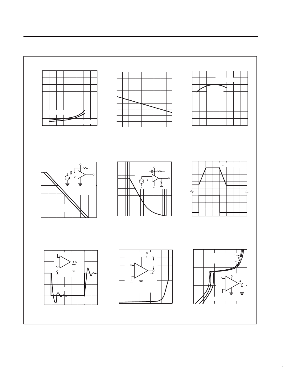
TYPICAL PERFORMANCE CHARACTERISTICS
V – OUTPUT VOL
T
AGE (V )
O
–
+
V
DC
100 k
Ω
V
O
1K
+
7
V
DC
V
IN
2 k
Ω
T
amb
= 0
°
C to +125
°
C
T
amb
= 55
°
C
4
3
2
1
0
0
10
20
30
40
SUPPLY VOLTAGE (V
DC
)
SUPPL
Y
CURRENT
DRAIN
(mA
) DC
90
80
70
60
50
40
30
20
10
0
55 35 –15
5
25
45 65
85 105 125
TEMPERATURE (
°
C)
OUTPUT
CURRENT
(mA
) DC
160
120
80
40
0
0
10
20
30
40
SUPPLY VOLTAGE (V
DC
)
R
L
+ 20 k
Ω
R
L
+ 2 k
Ω
A
— VOL
T
AGE
GAIN
(dB)
VOL
–
+
V+
10M
V
O
0.1
µ
f
V
+
/2
V
IN
V
+
= 30 V
DC
AND
–55
°
C
≤
T
amb
≤
+125
°
C
V
+
= 10 to 15 V
DC
AND
–55
°
C < T
amb
< +125
°
C
140
120
100
80
60
40
20
0
1
10
100
1k
10k
100k 1M 10M
FREQUENCY (Hz)
VOL
T
AGE GAIN (dB)
20
15
10
5
0
1k
10k
100k
1M
FREQUENCY (Hz)
V — OUTPUT SWING (V )
O
p–p
R
L
< 2 k
Ω
V
+
15 V
DC
4
3
2
1
0
3
2
1
0
0
10
20
30
40
TIME (
µ
s)
OUTPUT VOL
T
AGE
(V)
INPOUT VOL
T
AGE
(V)
E
O
50 pF
INPUT
OUTPUT
θ
IN
500
450
400
350
300
250
0
1
2
3
4
5
6
7
8
t — TIME (
µ
s)
T
amb
= +25
°
C
V+ = +30 V
DC
E – OUTPUT VOL
T
AGE (mV)
O
+V
+
/2
V+
V
2
I
O
INDEPENDENT OF V+
T
Aamb
= +25
°
C
8
7
6
5
4
3
2
1
0.001
0.01
0.1
1
10
100
I
O
+
– OUTPUT SOURCE CURRENT (mA
DC
)
V – OUTPUT VOL
T
AGE
REFERENCE
T
O
V+ (VD )
DC
∆
V
+
/2
V
+
I
O
T
amb
= +25
°
C
V
+
= +5 V
DC
V
+
= +15 V
DC
V
+
= +30 V
DC
10
1
0.1
0.01
0.001
0.01
0.1
1
10
100
I
O
– OUTPUT SINK CURRENT (mA
DC
)
DC
V
O
–
+
+
–
Supply Current
Current Limiting
Voltage Gain
Open-Loop
Frequency Response
Large-Signal
Frequency Response
Voltage-Follower
Response
Voltage-Follower
Pulse Response (Small-Signal)
Output Characteristics
Current Sourcing
Output Characteristics
Current Sinking
SL00284
Figure 3. Typical performance characteristics.
Philips Semiconductors
Product data
NE/SA/SE532/
LM258/358/A/2904
Low power dual operational amplifiers
2002 Jul 12
7
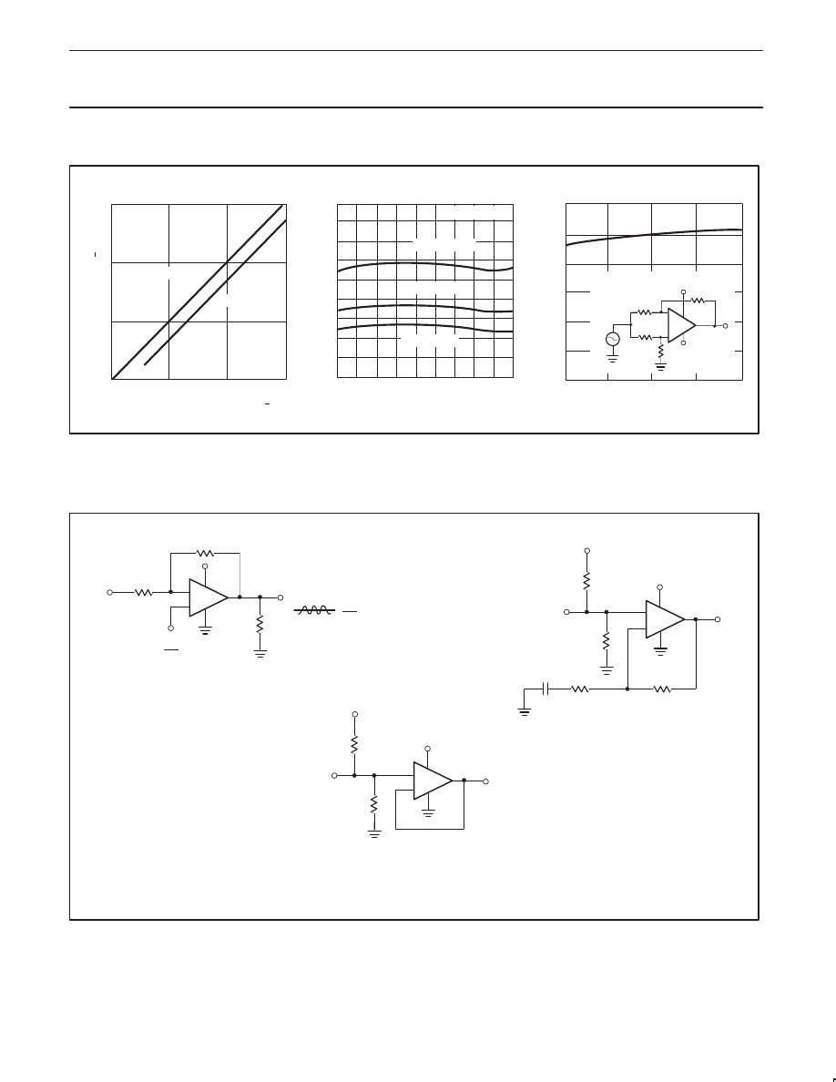
TYPICAL PERFORMANCE CHARACTERISTICS
(Continued)
+V — INPUT VOL
T
AGE ( V )
15
10
5
NEGATIVE
POSITIVE
0
5
10
15
V
+
OR V
–
— POWER SUPPLY VOLTAGE (+ V
DC
)
IN
DC
+
V
CM
= 0 V
DC
V
+
= +30 V
DC
V
+
= +15 V
DC
V
+
= +5 V
DC
90
80
70
60
50
40
30
20
10
0
–55 –35 –15
5
25
45
65
85 105 125
T
amb
— TEMPERATURE (
°
C)
I – INPUT CURRENT (nA
)
BD
C
100
Ω
100
Ω
7.5 V
DC
V
O
100 k
Ω
–
+
+
V
IN
+7.5 V
DC
120
100
80
60
40
20
0
100
1k
10k
100k
1M
f — FREQUENCY (Hz)
CMRR — COMMON–MODE REJECTION RA
TIO
(dB)
Input Voltage Range
Input Current
Common–Mode Rejection Ratio
SL00285
100 k
Ω
Figure 4. Typical performance characteristics (continued).
TYPICAL APPLICATIONS
V+
2
Non-Inverting Amplifier
RF
V+
8
RL
VO
RIN
V+
2
V
I
N
–
+
4
V+
8
VO
V
I
N
–
+
4
V+
10 k
Ω
V+
8
VO
V
I
N
–
+
4
V+
RF
BLOCKS
DC.
GAIN
R1
Single Supply Inverting Amplifier
Input Biasing Voltage Follower
SL00286
10 k
Ω
10 k
Ω
10 k
Ω
Figure 5. Typical applications.
Philips Semiconductors
Product data
NE/SA/SE532/
LM258/358/A/2904
Low power dual operational amplifiers
2002 Jul 12
8
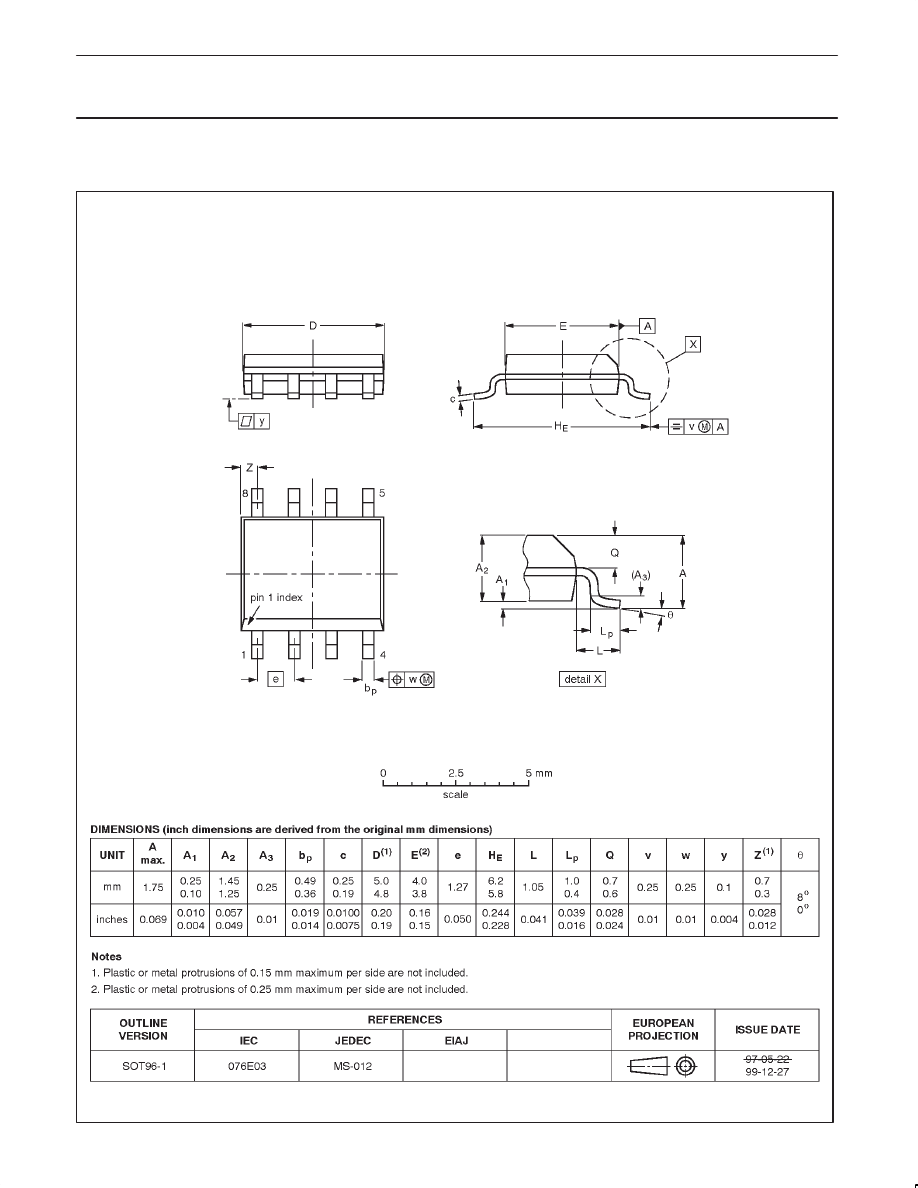
SO8:
plastic small outline package; 8 leads; body width 3.9 mm
SOT96-1
Philips Semiconductors
Product data
NE/SA/SE532/
LM258/358/A/2904
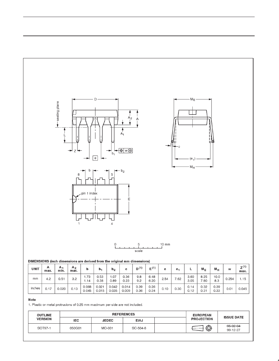
Low power dual operational amplifiers
2002 Jul 12
9
DIP8:
plastic dual in-line package; 8 leads (300 mil)
SOT97-1
Philips Semiconductors
Product data
NE/SA/SE532/
LM258/358/A/2904
Low power dual operational amplifiers
2002 Jul 12
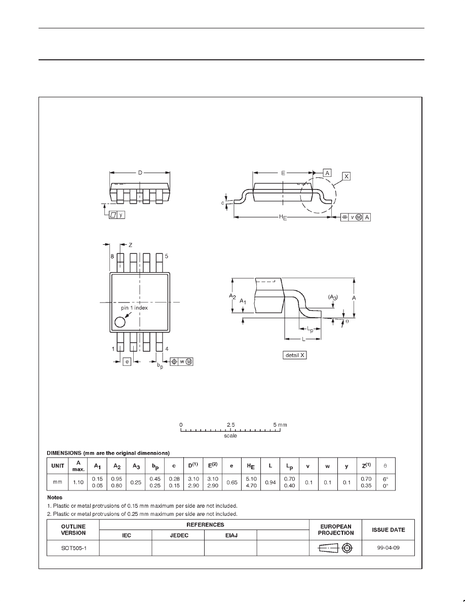
10
TSSOP8:
plastic thin shrink small outline package; 8 leads; body width 3 mm
SOT505-1

Philips Semiconductors
Product data
NE/SA/SE532/
LM258/358/A/2904
Low power dual operational amplifiers
2002 Jul 12
11
NOTES
Philips Semiconductors
Product data
NE/SA/SE532/
LM258/358/A/2904
Low power dual operational amplifiers
2002 Jul 12
12
Definitions
Short-form specification — The data in a short-form specification is extracted from a full data sheet with the same type number and title. For
detailed information see the relevant data sheet or data handbook.
Limiting values definition — Limiting values given are in accordance with the Absolute Maximum Rating System (IEC 60134). Stress above one
or more of the limiting values may cause permanent damage to the device. These are stress ratings only and operation of the device at these or
at any other conditions above those given in the Characteristics sections of the specification is not implied. Exposure to limiting values for extended
periods may affect device reliability.
Application information — Applications that are described herein for any of these products are for illustrative purposes only. Philips
Semiconductors make no representation or warranty that such applications will be suitable for the specified use without further testing or
modification.
Disclaimers
Life support — These products are not designed for use in life support appliances, devices or systems where malfunction of these products can
reasonably be expected to result in personal injury. Philips Semiconductors customers using or selling these products for use in such applications
do so at their own risk and agree to fully indemnify Philips Semiconductors for any damages resulting from such application.
Right to make changes — Philips Semiconductors reserves the right to make changes, without notice, in the products, including circuits, standard
cells, and/or software, described or contained herein in order to improve design and/or performance. Philips Semiconductors assumes no
responsibility or liability for the use of any of these products, conveys no license or title under any patent, copyright, or mask work right to these
products, and makes no representations or warranties that these products are free from patent, copyright, or mask work right infringement, unless
otherwise specified.
Contact information
For additional information please visit
http://www.semiconductors.philips.com.
Fax: +31 40 27 24825
For sales offices addresses send e-mail to:
sales.addresses@www.semiconductors.philips.com.
Koninklijke Philips Electronics N.V. 2002
All rights reserved. Printed in U.S.A.
Date of release: 08-02
Document order number:
9397 750 10187
Data sheet status
[1]
Objective data
Preliminary data
Product data
Product
status
[2]
Development
Qualification
Production
Definitions
This data sheet contains data from the objective specification for product development.
Philips Semiconductors reserves the right to change the specification in any manner without notice.
This data sheet contains data from the preliminary specification. Supplementary data will be
published at a later date. Philips Semiconductors reserves the right to change the specification
without notice, in order to improve the design and supply the best possible product.
This data sheet contains data from the product specification. Philips Semiconductors reserves the
right to make changes at any time in order to improve the design, manufacturing and supply.
Changes will be communicated according to the Customer Product/Process Change Notification
(CPCN) procedure SNW-SQ-650A.
Data sheet status
[1] Please consult the most recently issued data sheet before initiating or completing a design.
[2] The product status of the device(s) described in this data sheet may have changed since this data sheet was published. The latest information is available on the Internet at URL
http://www.semiconductors.philips.com.

This datasheet has been download from:
Datasheets for electronics components.
Document Outline
- DESCRIPTION
- PIN CONFIGURATION
- UNIQUE FEATURES
- FEATURES
- EQUIVALENT CIRCUIT
- ORDERING INFORMATION
- ABSOLUTE MAXIMUM RATINGS
- DC ELECTRICAL CHARACTERISTICS
- DC ELECTRICAL CHARACTERISTICS
- TYPICAL PERFORMANCE CHARACTERISTICS
- TYPICAL PERFORMANCE CHARACTERISTICS
- TYPICAL APPLICATIONS
- PACKAGE OUTLINE
- Data sheet status
- Definitions
- Disclaimers
Wyszukiwarka
Podobne podstrony:
LM158 LM258 LM358
LM358
lm2904
ne532
LM358
lm358 n
fetch datenblatt lm358
lm358
lm358
lm358
LM2904
lm358 2
LM358 2
więcej podobnych podstron