UNISONIC TECHNOLOGIES CO., LTD
LM358
LINEAR INTEGRATED CIRCUIT
www.unisonic.com.tw
1 of 7
Copyright © 2005 Unisonic Technologies Co., Ltd
QW-R105-001,H
DUAL OPERATIONAL
AMPLIFIER
DESCRIPTION
The UTC LM358 consists of two independent high gain, internally
frequency compensated operational amplifier. It can be operated
from a single power supply and also split power supplies.
FEATURES
*Internally frequency compensated for unity gain.
*Wide power supply range 3V - 32V.
*Input common-mode voltage range include ground.
*Large DC voltage gain.
*Pb-free plating product number: LM358L
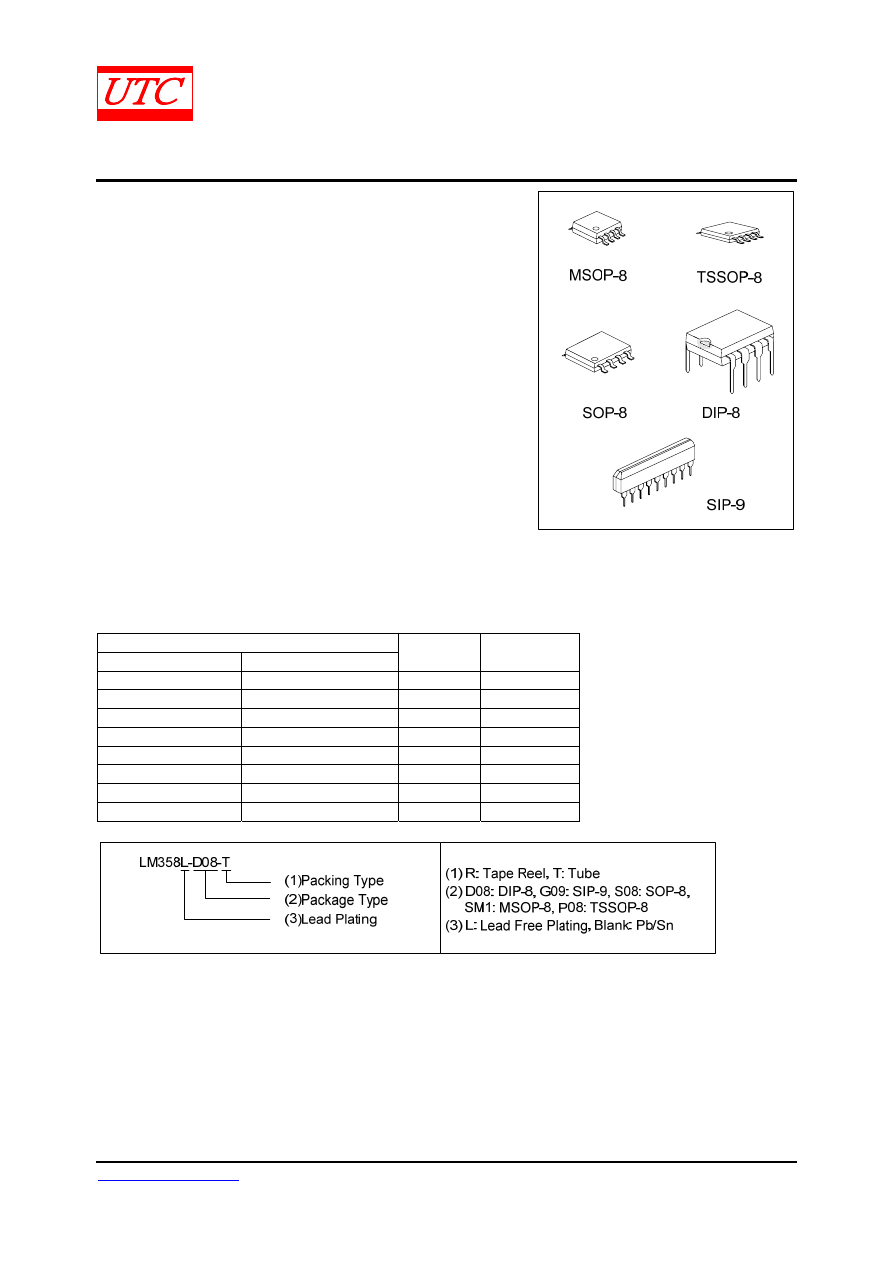
ORDERING INFORMATION
Ordering Number
Normal
Lead Free Plating
Package Packing
LM358-D08-T LM358L-D08-T
DIP-8 Tube
LM358-G09-T LM358L-G09-T SIP-9 Tube
LM358-P08-R LM358L-P08-R
TSSOP-8
Tape
Reel
LM358-P08-T LM358L-P08-T
TSSOP-8
Tube
LM358-S08-R LM358L-S08-R
SOP-8
Tape
Reel
LM358-S08-T LM358L-S08-T
SOP-8
Tube
LM358-SM1-R LM358L-SM1-R
MSOP-8
Tape
Reel
LM358-SM1-T LM358L-SM1-T
MSOP-8
Tube
LM358
LINEAR INTEGRATED CIRCUIT
UNISONIC TECHNOLOGIES CO., LTD
2 of 7
www.unisonic.com.tw
QW-R105-001,H
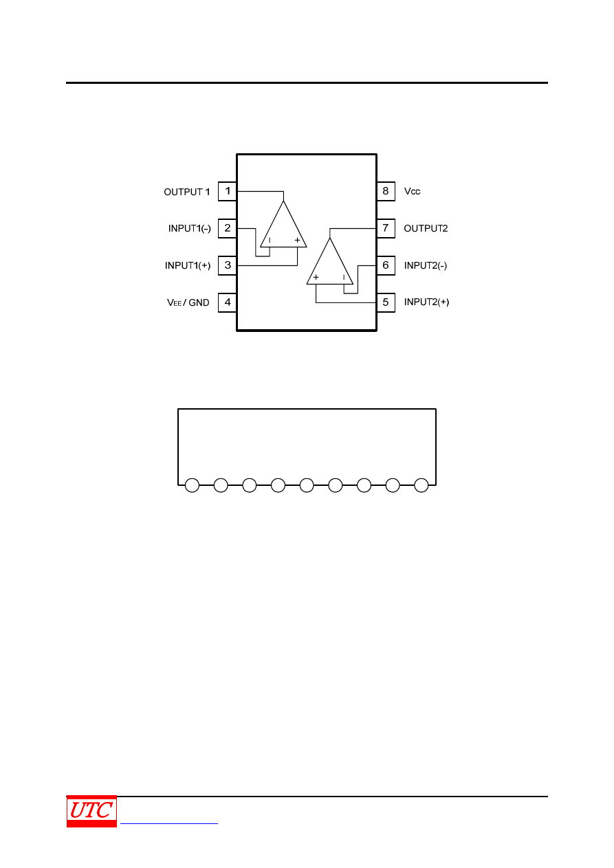
PIN DESCRIPTION
SOP-8/DIP-8/MSOP-8/TSSOP-8
SIP-9
1
2
3
4
5
6
7
8
9
V
CC
OUT1 IN1(-) IN1(+) GND
IN2(+)
OUT2
V
CC
IN2(-)
LM358
LINEAR INTEGRATED CIRCUIT
UNISONIC TECHNOLOGIES CO., LTD
3 of 7
www.unisonic.com.tw
QW-R105-001,H
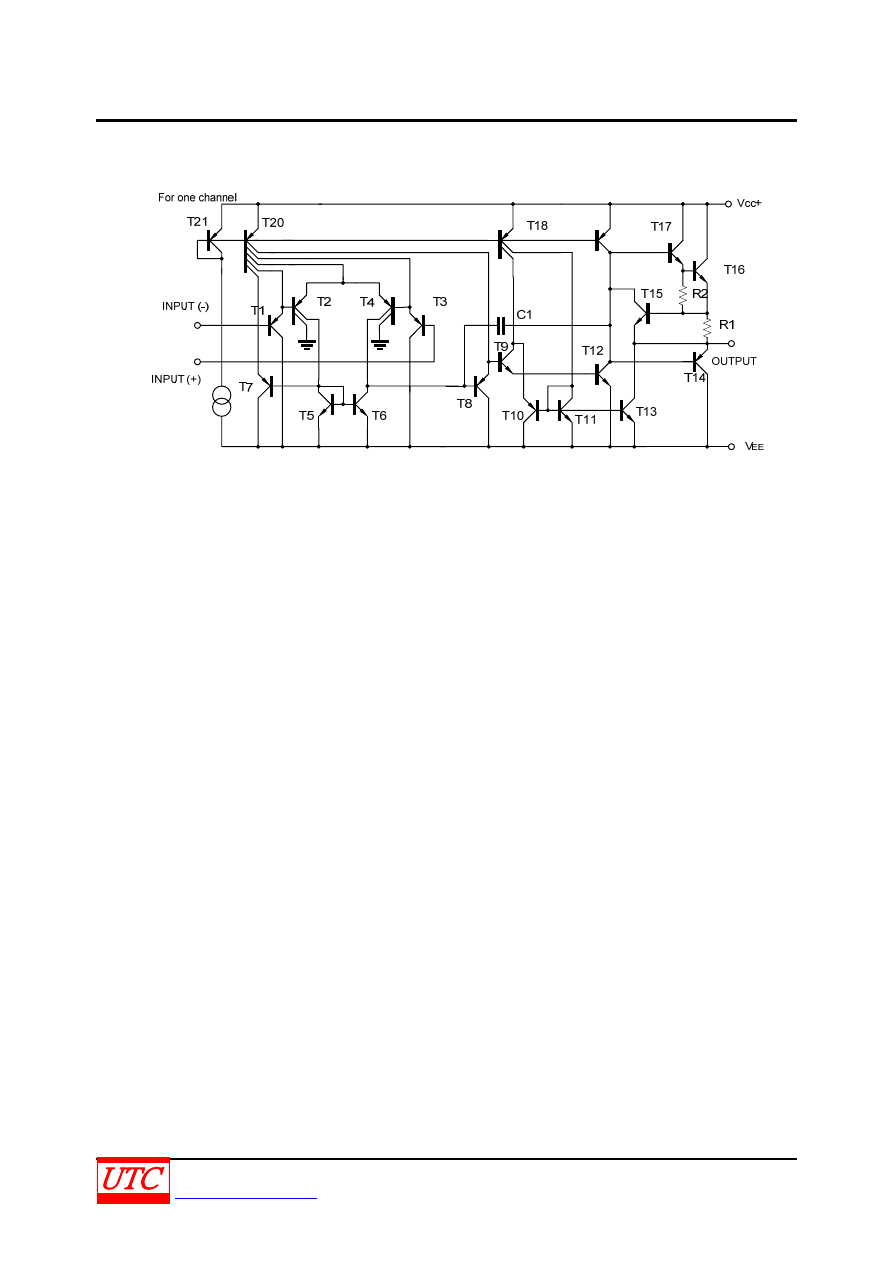
BLOCK DIAGRAM
LM358
LINEAR INTEGRATED CIRCUIT
UNISONIC TECHNOLOGIES CO., LTD
4 of 7
www.unisonic.com.tw
QW-R105-001,H
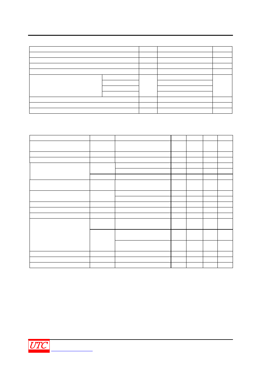
ABSOLUTE MAXIMUM RATINGS
PARAMETER SYMBOL
RATINGS
UNIT
Supply Voltage
V
CC
±16 or 32
V
Differential Input Voltage
V
I(DIFF)
±32 V
Input Voltage
V
I
-0.3 ~ +32
V
Output Short to Ground
Continuous
SIP-9 600
DIP-8 500
SOP-8 280
Power Dissipation
TSSOP-8/MSOP-8
P
D
200
mW
Junction Temperature
T
J
+125
°C
Operating Temperature
T
OPR
0 ~ +70
°C
Storage Temperature
T
STG
-65 ~ +150
°C
Note Absolute maximum ratings are those values beyond which the device could be permanently damaged.
Absolute maximum ratings are stress ratings only and functional device operation is not implied.
ELECTRICAL CHARACTERISTICS
(V
CC
=5.0V, V
EE
=GND, Ta=25℃, unless otherwise specified)
PARAMETER SYMBOL
TEST
CONDITIONS
MIN
TYP
MAX
UNIT
Input Offset Voltage
V
I(OFF)
V
CM
=0V toV
CC
-1.5V
V
O(P)
=1.4V, R
S
=0
Ω
2.9
7.0
mV
Input Common Mode Voltage
V
I(CM)
V
CC
=30V 0
V
CC
-1.5
V
Differential Input Voltage
V
I(DIFF)
V
CC
V
V
CC
=30V, R
L
=2K
Ω 26
V
V
OH
V
CC
=30V, R
L
=10K
Ω 27
28
V
Output Voltage Swing
V
OL
V
CC
=5V, R
L
≧10K
Ω
5
20
mV
Large Signal Voltage Gain
G
V
V
CC
=15V, R
L
≧2K
Ω
V
O(P)
=1V ~ 11V
25 100 V/mV
R
L
=
∝, V
CC
=30V
0.8
2.0
mA
Power Supply Current
I
CC
R
L
=
∝, Full Temperature Range
0.5
1.2
mA
Input Offset Current
I
I(OFF)
5 50 nA
Input Bias Current
I
I(BIAS)
45 250 nA
Short Circuit Current to Ground
I
SC
40 60 mA
I
SOURCE
V
I
(+)=1V, V
I
(-)=0V
V
CC
=15V, V
O(P)
=2V
10 30 mA
V
I
(+)=0V, V
I
(-)=1V
V
CC
=15V, V
O(P)
=2V
10 15 mA
Output Current
I
SINK
V
I
(+)=0V, V
I
(-)=1V
V
CC
=15V, V
O(P)
=200mV
12 100 mA
Common Mode Rejection Ratio
CMRR
65
80
dB
Power Supply Rejection Ratio
PSRR
65
100
dB
Channel Separation
CS
f=1KHZ ~ 20KHZ
120
dB
LM358
LINEAR INTEGRATED CIRCUIT
UNISONIC TECHNOLOGIES CO., LTD
5 of 7
www.unisonic.com.tw
QW-R105-001,H
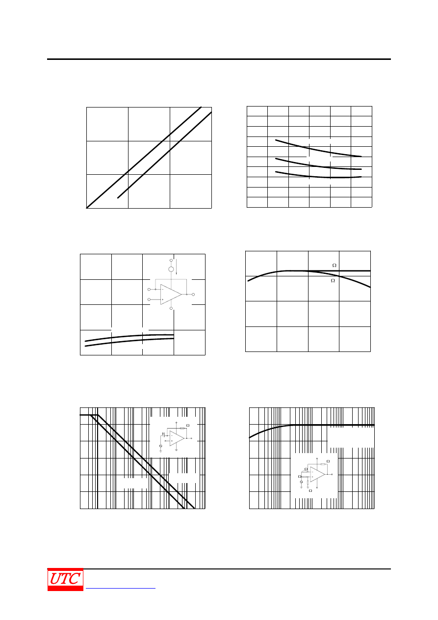
TYPICAL CHARACTERISTICS
0
5
10
15
5
0
10
15
Fig.1 Input Voltage Range
Inpu
t Vo
ltage
Positive
Input
Negative
Input
-50
-25
0
25
50
75
100
0
20
40
60
80
100
Vcc=+15V
Vcc=+5V
Vcc=+30V
Fig.2 Input Current vs Temperature
Inpu
t Cu
rren
t (mA)
0
10
20
30
40
0
10
20
30
40
Vcc
Ic
Fig.3 Input Current vs Supply Voltage
Inp
u
t C
u
rre
nt (m
A)
Supply Voltage (V)
0
7.5
15
22.5
30
0
40
80
120
160
Fig. 4 Voltage Gain vs Supply Voltage
Voltag
e Gain
æ
(dB)
Supply Voltage (V)
RL=20k
RL=2k
Vo
ltag
e Ga
in
(d
B)
0
20
40
60
80
120
100
10
0
1
10
2
10
3
10
4
10
5
10
6
10
7
10
Frequency (Hz)
Vcc=30V
Vcc=15V
0.1 F
100M
Vcc
Vin
Vcc/2
2
10
3
10
4
10
5
10
6
10
0
20
40
60
80
100
120
C
o
mm
on Mod
e
Re
jecti
on Ra
ti
o
(d
B)
Frequency (Hz)
100k
-7.5V
100
100
100k
+7.5V
Vin
Vcc=+7.5V
Vee=-7.5V
Fig. 6 Common Mode Rejection Ratio vs Frequency
Fig. 5 Open Loop Gain vs Frequency
Temperature(°C)
Power Supply Voltage
Ta= 0~+85°C
Ta= -20°C
LM358
LINEAR INTEGRATED CIRCUIT
UNISONIC TECHNOLOGIES CO., LTD
6 of 7
www.unisonic.com.tw
QW-R105-001,H
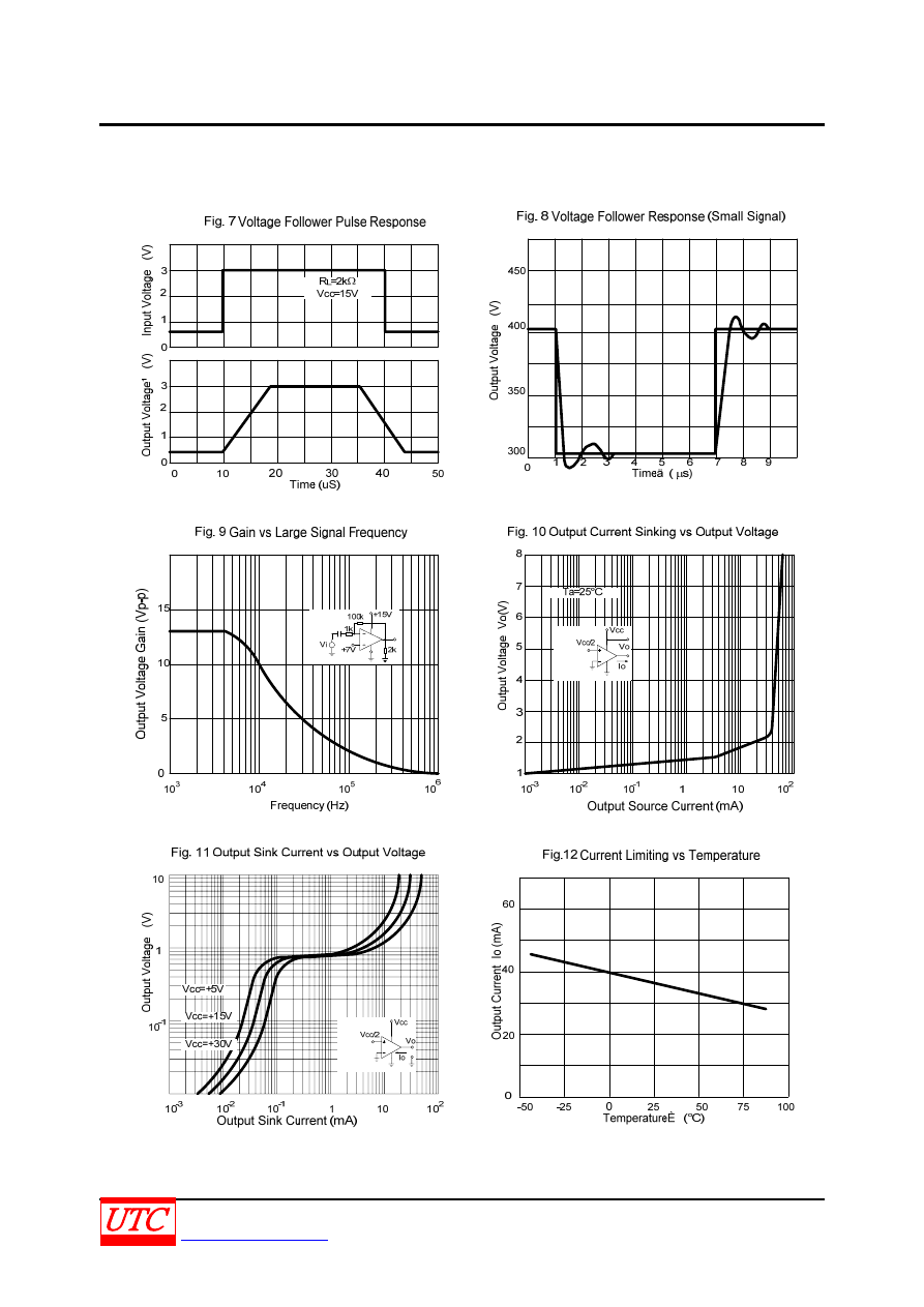
TYPICAL CHARACTERISTICS(Cont.)

LM358
LINEAR INTEGRATED CIRCUIT
UNISONIC TECHNOLOGIES CO., LTD
7 of 7
www.unisonic.com.tw
QW-R105-001,H
UTC assumes no responsibility for equipment failures that result from using products at values that
exceed, even momentarily, rated values (such as maximum ratings, operating condition ranges, or
other parameters) listed in products specifications of any and all UTC products described or contained
herein. UTC products are not designed for use in life support appliances, devices or systems where
malfunction of these products can be reasonably expected to result in personal injury. Reproduction in
whole or in part is prohibited without the prior written consent of the copyright owner. The information
presented in this document does not form part of any quotation or contract, is believed to be accurate
and reliable and may be changed without notice.
Wyszukiwarka
Podobne podstrony:
LM358
LM358
lm358 n
fetch datenblatt lm358
lm358
lm358
LM258 LM358 LM2904 NE532 SA532 SE532
lm358 2
LM358 2
LM158 LM258 LM358
LM358 D
więcej podobnych podstron