Semiconductor Components Industries, LLC, 2004
April, 2004 − Rev. 16
1
Publication Order Number:
LM358/D
LM358, LM258, LM2904,
LM2904A, LM2904V,
NCV2904
Single Supply Dual
Operational Amplifiers
Utilizing the circuit designs perfected for Quad Operational
Amplifiers, these dual operational amplifiers feature low power drain,
a common mode input voltage range extending to ground/V
EE
, and
single supply or split supply operation. The LM358 series is
equivalent to one−half of an LM324.
These amplifiers have several distinct advantages over standard
operational amplifier types in single supply applications. They can
operate at supply voltages as low as 3.0 V or as high as 32 V, with
quiescent currents about one−fifth of those associated with the
MC1741 (on a per amplifier basis). The common mode input range
includes the negative supply, thereby eliminating the necessity for
external biasing components in many applications. The output voltage
range also includes the negative power supply voltage.
Features
•
Short Circuit Protected Outputs
•
True Differential Input Stage
•
Single Supply Operation: 3.0 V to 32 V (LM258/LM358)
3.0 V to 26 V (LM2904, A, V)
•
Low Input Bias Currents
•
Internally Compensated
•
Common Mode Range Extends to Negative Supply
•
Single and Split Supply Operation
•
ESD Clamps on the Inputs Increase Ruggedness of the Device
without Affecting Operation
•
Pb−Free Packages are Available
PDIP−8
N, AN, VN SUFFIX
CASE 626
1
8
SOIC−8
D, VD SUFFIX
CASE 751
1
8
PIN CONNECTIONS
V
EE
/Gnd
Inputs A
Inputs B
Output B
Output A
V
CC
−
−
+
+
1
2
3
4
8
7
6
5
(Top View)
See general marking information in the device marking
section on page 11 of this data sheet.
DEVICE MARKING INFORMATION
See detailed ordering and shipping information in the package
dimensions section on page 10 of this data sheet.
ORDERING INFORMATION
Micro8
DMR2 SUFFIX
CASE 846A
1
8
http://onsemi.com
LM358, LM258, LM2904, LM2904A, LM2904V, NCV2904
http://onsemi.com
2
Single Supply
Split Supplies
V
CC
V
EE
/Gnd
3.0 V to V
CC(max)
1
2
V
CC
1
2
V
EE
1.5 V to V
CC(max)
1.5 V to V
EE(max)
Output
Bias Circuitry
Common to Both
Amplifiers
V
CC
V
EE
/Gnd
Inputs
Q2
Q3
Q4
Q5
Q26
Q7
Q8
Q6
Q9
Q11
Q10
Q1
2.4 k
Q25
Q22
40 k
Q13
Q14
Q15
Q16
Q19
5.0 pF
Q18
Q17
Q20
Q21
2.0 k
Q24
Q23
Q12
25
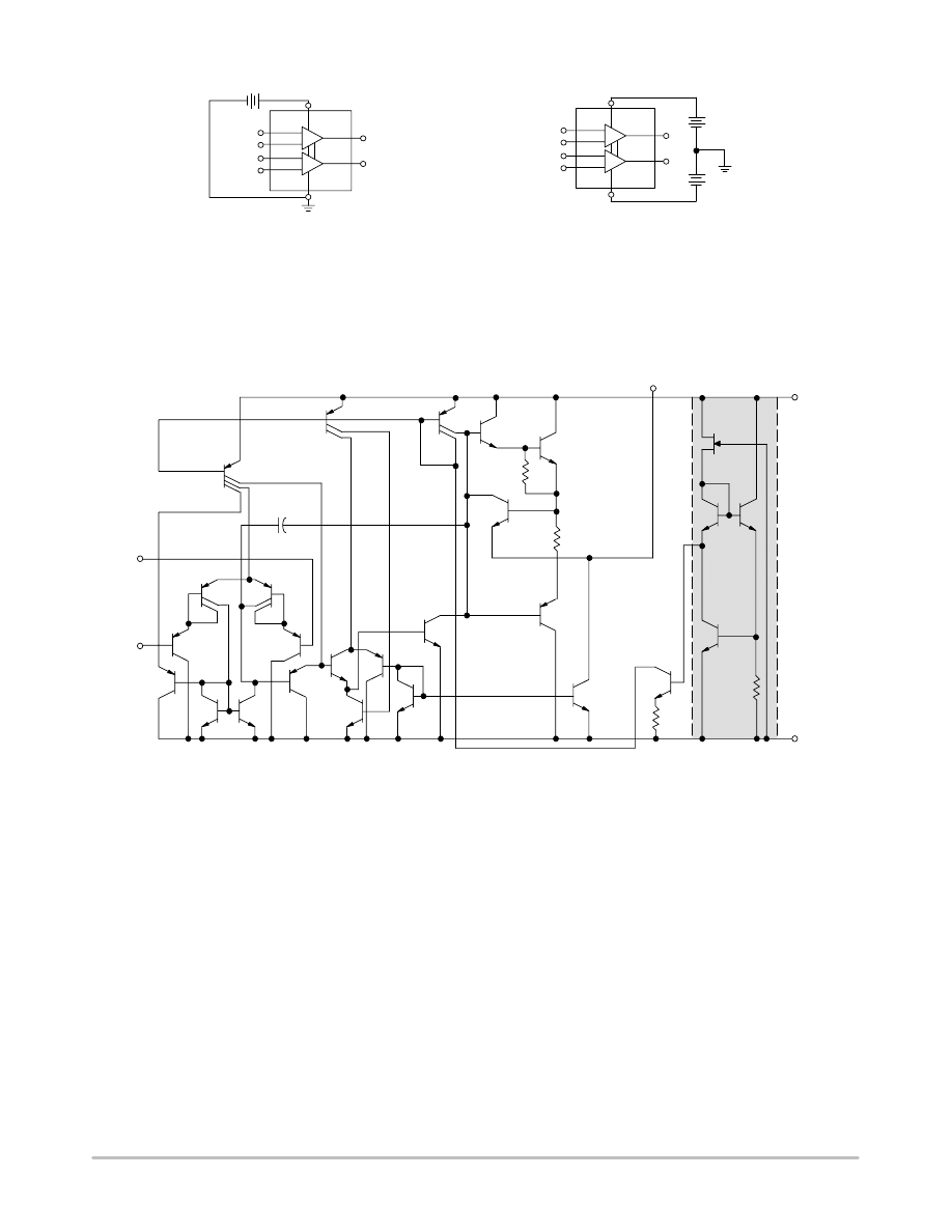
Figure 1.
Figure 2. Representative Schematic Diagram
(One−Half of Circuit Shown)
LM358, LM258, LM2904, LM2904A, LM2904V, NCV2904
http://onsemi.com
3
MAXIMUM RATINGS
(T
A
= +25
°
C, unless otherwise noted.)
Rating
Symbol
LM258
LM358
LM2904, LM2904A
LM2904V, NCV2904
Unit
Power Supply Voltages
Single Supply
Split Supplies
V
CC
V
CC
, V
EE
32
±
16
26
±
13
Vdc
Input Differential Voltage Range (Note 1)
V
IDR
±
32
±
26
Vdc
Input Common Mode Voltage Range (Note 2)
V
ICR
−0.3 to 32
−0.3 to 26
Vdc
Output Short Circuit Duration
t
SC
Continuous
Junction Temperature
T
J
150
°
C
Thermal Resistance, Junction−to−Air (Note 3)
R
JA
238
°
C/W
Storage Temperature Range
T
stg
−55 to +125
°
C
ESD Protection at any Pin
Human Body Model
Machine Model
V
esd
2000
200
V
Operating Ambient Temperature Range
LM258
LM358
LM2904/LM2904A
LM2904V, NCV2904 (Note 4)
T
A
−25 to +85
0 to +70
−
−
−
−
−40 to +105
−40 to +125
°
C
1. Split Power Supplies.
2. For Supply Voltages less than 32 V for the LM258/358 and 26 V for the LM2904, A, V, the absolute maximum input voltage is equal to the
supply voltage.
3. R
JA
for Case 846A.
4.
NCV2904 is qualified for automotive use.
LM358, LM258, LM2904, LM2904A, LM2904V, NCV2904
http://onsemi.com
4
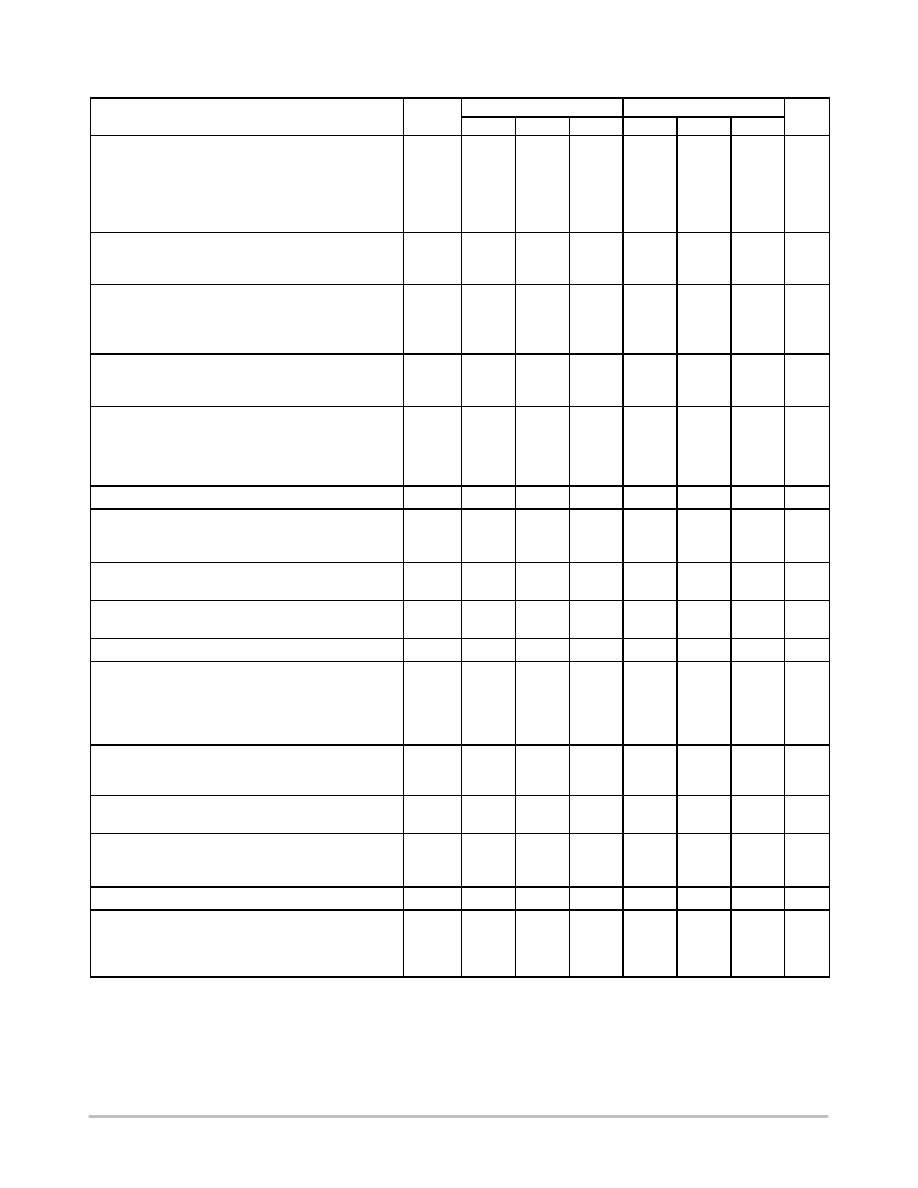
ELECTRICAL CHARACTERISTICS
(V
CC
= 5.0 V, V
EE
= GND, T
A
= 25
°
C, unless otherwise noted.)
LM258
LM358
Characteristic
Symbol
Min
Typ
Max
Min
Typ
Max
Unit
Input Offset Voltage
V
CC
= 5.0 V to 30 V (26 V for LM2904, V),
V
IC
= 0 V to V
CC
−1.7 V, V
O
1.4 V, R
S
= 0
V
IO
mV
T
A
= 25
°
C
−
2.0
5.0
−
2.0
7.0
T
A
= T
high
−
−
7.0
−
−
9.0
T
A
= T
low
−
−
7.0
−
−
9.0
Average Temperature Coefficient of Input Offset
Voltage
V
IO
/
T
−
7.0
−
−
7.0
−
V/
°
C
T
A
= T
high
to T
low
Input Offset Current
I
IO
−
3.0
30
−
5.0
50
nA
T
A
= T
high
to T
low
−
−
100
−
−
150
Input Bias Current
I
IB
−
−45
−150
−
−45
−250
T
A
= T
high
to T
low
−
−50
−300
−
−50
−500
Average Temperature Coefficient of Input Offset
Current
I
IO
/
T
−
10
−
−
10
−
pA/
°
C
T
A
= T
high
to T
low
Input Common Mode Voltage Range (Note 6),
V
CC
= 30 V
(26 V for LM2904, V)
V
ICR
0
−
28.3
0
−
28.3
V
V
CC
= 30 V (26 V for LM2904, V),
T
A
= T
high
to T
low
0
−
28
0
−
28
Differential Input Voltage Range
V
IDR
−
−
V
CC
−
−
V
CC
V
Large Signal Open Loop Voltage Gain
A
VOL
V/mV
R
L
= 2.0 k
, V
CC
= 15 V, For Large V
O
Swing,
50
100
−
25
100
−
T
A
= T
high
to T
low
25
−
−
15
−
−
Channel Separation
CS
−
−120
−
−
−120
−
dB
1.0 kHz
≤
f
≤
20 kHz, Input Referenced
Common Mode Rejection
CMR
70
85
−
65
70
−
dB
R
S
≤
10 k
Power Supply Rejection
PSR
65
100
−
65
100
−
dB
Output Voltage−High Limit
T
A
= T
high
to T
low
V
OH
V
V
CC
= 5.0 V, R
L
= 2.0 k
, T
A
= 25
°
C
3.3
3.5
−
3.3
3.5
−
V
CC
= 30 V (26 V for LM2904, V), R
L
= 2.0 k
26
−
−
26
−
−
V
CC
= 30 V (26 V for LM2904, V), R
L
= 10 k
27
28
−
27
28
−
Output Voltage−Low Limit
V
OL
−
5.0
20
−
5.0
20
mV
V
CC
= 5.0 V, R
L
= 10 k
,
T
A
= T
high
to T
low
Output Source Current
I
O
+
20
40
−
20
40
−
mA
V
ID
= +1.0 V, V
CC
= 15 V
Output Sink Current
I
O
−
V
ID
= −1.0 V, V
CC
= 15 V
10
20
−
10
20
−
mA
V
ID
= −1.0 V, V
O
= 200 mV
12
50
−
12
50
−
A
Output Short Circuit to Ground (Note 7)
I
SC
−
40
60
−
40
60
mA
Power Supply Current (Total Device)
T
A
= T
high
to T
low
I
CC
mA
V
CC
= 30 V (26 V for LM2904, V), V
O
= 0 V, R
L
=
∞
−
1.5
3.0
−
1.5
3.0
V
CC
= 5 V, V
O
= 0 V, R
L
=
∞
−
0.7
1.2
−
0.7
1.2
5. LM258: T
low
= −25
°
C, T
high
= +85
°
C
LM358: T
low
= 0
°
C, T
high
= +70
°
C
LM2904/LM2904A: T
low
= −40
°
C, T
high
= +105
°
C
LM2904V & NCV2904: T
low
= −40
°
C, T
high
= +125
°
C
NCV2904 is qualified for automotive use.
6. The input common mode voltage or either input signal voltage should not be allowed to go negative by more than 0.3 V. The upper end of
the common mode voltage range is V
CC
−1.7 V.
7. Short circuits from the output to V
CC
can cause excessive heating and eventual destruction. Destructive dissipation can result from
simultaneous shorts on all amplifiers.
LM358, LM258, LM2904, LM2904A, LM2904V, NCV2904
http://onsemi.com
5
ELECTRICAL CHARACTERISTICS
(V
CC
= 5.0 V, V
EE
= Gnd, T
A
= 25
°
C, unless otherwise noted.)
LM2904
LM2904A
LM2904V, NCV2904
Characteristic
Symbol
Min
Typ
Max
Min
Typ
Max
Min
Typ
Max
Unit
Input Offset Voltage
V
CC
= 5.0 V to 30 V (26 V for LM2904, V),
V
IC
= 0 V to V
CC
−1.7 V, V
O
1.4 V, R
S
= 0
V
IO
mV
T
A
= 25
°
C
−
2.0
7.0
−
2.0
7.0
−
−
7.0
T
A
= T
high
−
−
10
−
−
10
−
−
13
T
A
= T
low
−
−
10
−
−
10
−
−
10
Average Temperature Coefficient of Input Offset
Voltage
V
IO
/
T
−
7.0
−
−
7.0
−
−
7.0
−
V/
°
C
T
A
= T
high
to T
low
Input Offset Current
I
IO
−
5.0
50
−
5.0
50
−
5.0
50
nA
T
A
= T
high
to T
low
−
45
200
−
45
200
−
45
200
Input Bias Current
I
IB
−
−45
−250
−
−45
−100
−
−45
−250
T
A
= T
high
to T
low
−
−50
−500
−
−50
−250
−
−50
−500
Average Temperature Coefficient of Input Offset
Current
I
IO
/
T
−
10
−
−
10
−
−
10
−
pA/
°
C
T
A
= T
high
to T
low
Input Common Mode Voltage Range (Note 9),
V
CC
= 30 V (26 V for LM2904, V)
V
ICR
0
−
24.3
0
−
24.3
0
−
24.3
V
V
CC
= 30 V (26 V for LM2904, V),
T
A
= T
high
to T
low
0
−
24
0
−
24
0
−
24
Differential Input Voltage Range
V
IDR
−
−
V
CC
−
−
V
CC
−
−
V
CC
V
Large Signal Open Loop Voltage Gain
A
VOL
V/mV
R
L
= 2.0 k
, V
CC
= 15 V, For Large V
O
Swing,
25
100
−
25
100
−
25
100
−
T
A
= T
high
to T
low
15
−
−
15
−
−
15
−
−
Channel Separation
CS
−
−120
−
−
−120
−
−
−120
−
dB
1.0 kHz
≤
f
≤
20 kHz, Input Referenced
Common Mode Rejection
CMR
50
70
−
50
70
−
50
70
−
dB
R
S
≤
10 k
Power Supply Rejection
PSR
50
100
−
50
100
−
50
100
−
dB
Output Voltage−High Limit
T
A
= T
high
to T
low
V
OH
V
V
CC
= 5.0 V, R
L
= 2.0 k
, T
A
= 25
°
C
3.3
3.5
−
3.3
3.5
−
3.3
3.5
−
V
CC
= 30 V (26 V for LM2904, V), R
L
= 2.0 k
22
−
−
22
−
−
22
−
−
V
CC
= 30 V (26 V for LM2904, V), R
L
= 10 k
23
24
−
23
24
−
23
24
−
Output Voltage−Low Limit
V
OL
−
5.0
20
−
5.0
20
−
5.0
20
mV
V
CC
= 5.0 V, R
L
= 10 k
,
T
A
= T
high
to T
low
Output Source Current
I
O
+
20
40
−
20
40
−
20
40
−
mA
V
ID
= +1.0 V, V
CC
= 15 V
Output Sink Current
I
O
−
V
ID
= −1.0 V, V
CC
= 15 V
10
20
−
10
20
−
10
20
−
mA
V
ID
= −1.0 V, V
O
= 200 mV
−
−
−
−
−
−
−
−
−
A
Output Short Circuit to Ground (Note 10)
I
SC
−
40
60
−
40
60
−
40
60
mA
Power Supply Current (Total Device)
T
A
= T
high
to T
low
I
CC
mA
V
CC
= 30 V (26 V for LM2904, V), V
O
= 0 V,
R
L
=
∞
−
1.5
3.0
−
1.5
3.0
−
1.5
3.0
V
CC
= 5 V, V
O
= 0 V, R
L
=
∞
−
0.7
1.2
−
0.7
1.2
−
0.7
1.2
8. LM258: T
low
= −25
°
C, T
high
= +85
°
C
LM358: T
low
= 0
°
C, T
high
= +70
°
C
LM2904/LM2904A: T
low
= −40
°
C, T
high
= +105
°
C
LM2904V & NCV2904: T
low
= −40
°
C, T
high
= +125
°
C
NCV2904 is qualified for automotive use.
9. The input common mode voltage or either input signal voltage should not be allowed to go negative by more than 0.3 V. The upper end of
the common mode voltage range is V
CC
−1.7 V.
10. Short circuits from the output to V
CC
can cause excessive heating and eventual destruction. Destructive dissipation can result from
simultaneous shorts on all amplifiers.
LM358, LM258, LM2904, LM2904A, LM2904V, NCV2904
http://onsemi.com
6
CIRCUIT DESCRIPTION
The LM358 series is made using two internally
compensated, two−stage operational amplifiers. The first
stage of each consists of differential input devices Q20 and
Q18 with input buffer transistors Q21 and Q17 and the
differential to single ended converter Q3 and Q4. The first
stage performs not only the first stage gain function but also
performs the level shifting and transconductance reduction
functions. By reducing the transconductance, a smaller
compensation capacitor (only 5.0 pF) can be employed, thus
saving chip area. The transconductance reduction is
accomplished by splitting the collectors of Q20 and Q18.
Another feature of this input stage is that the input common
mode range can include the negative supply or ground, in
single supply operation, without saturating either the input
devices or the differential to single−ended converter. The
second stage consists of a standard current source load
amplifier stage.
Each amplifier is biased from an internal−voltage
regulator which has a low temperature coefficient thus
giving each amplifier good temperature characteristics as
well as excellent power supply rejection.
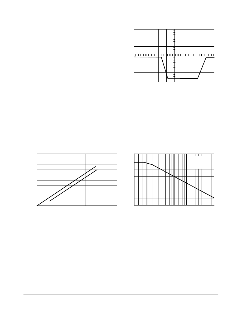
Figure 3. Large Signal Voltage
Follower Response
5.0
s/DIV
1.0 V/DIV
V
CC
= 15 Vdc
R
L
= 2.0 k
T
A
= 25
°
C
A
VOL
, OPEN LOOP
VOL
TAGE GAIN (dB)
V , INPUT
VOL
TAGE (V)
I
Figure 4. Input Voltage Range
Figure 5. Large−Signal Open Loop Voltage Gain
18
16
14
12
10
8.0
6.0
4.0
2.0
0
20
0
2.0
4.0
6.0
8.0
10
12
14
16
18
20
V
CC
/V
EE,
POWER SUPPLY VOLTAGES (V)
120
100
80
60
40
20
0
−20
1.0
10
100
1.0 k
10 k
100 k
1.0 M
f, FREQUENCY (Hz)
Negative
Positive
V
CC
= 15 V
V
EE
= Gnd
T
A
= 25
°
C
LM358, LM258, LM2904, LM2904A, LM2904V, NCV2904
http://onsemi.com
7
V
OR
, OUTPUT
VOL
TAGE RANGE (V
)
pp
V
O
, OUTPUT
VOL
TAGE (mV)
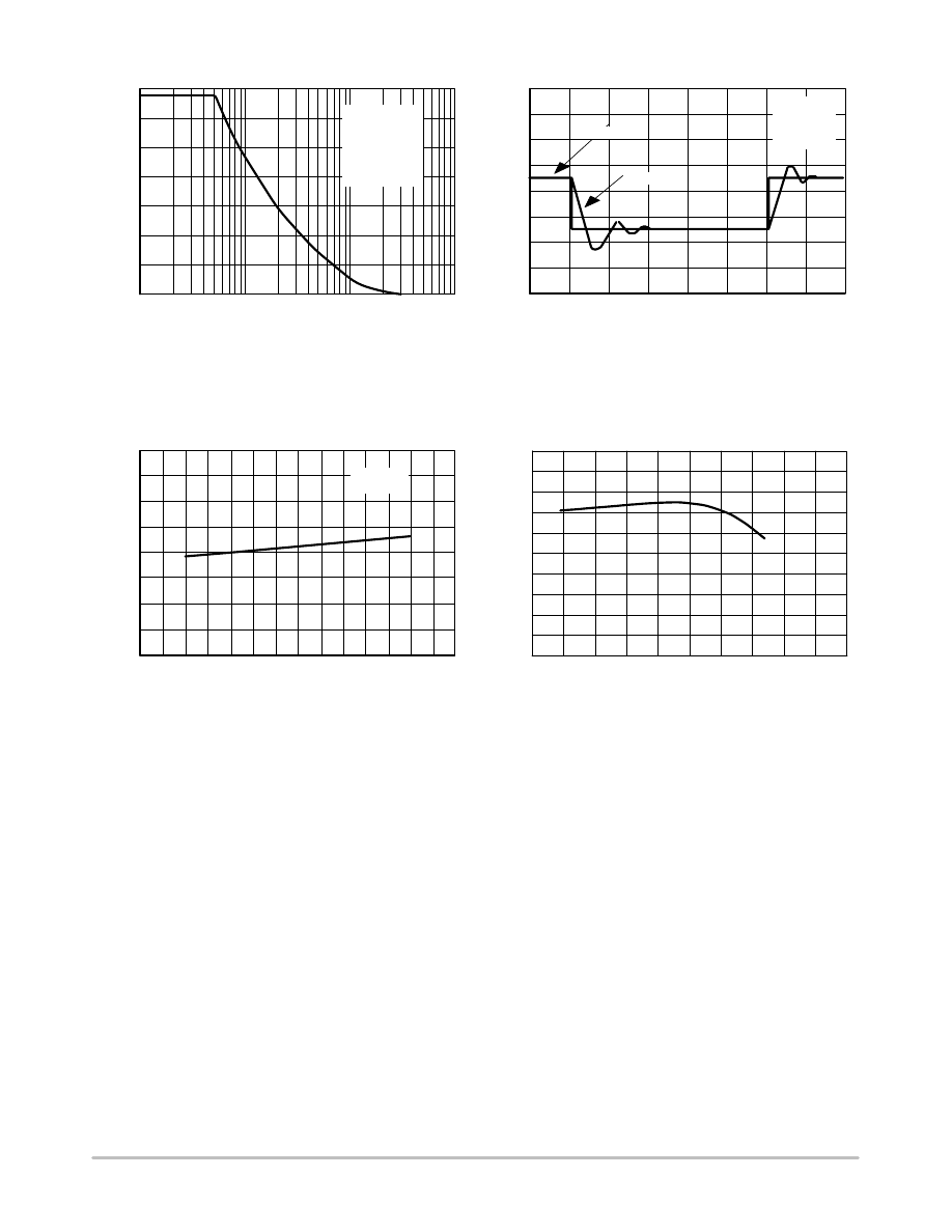
Figure 6. Large−Signal Frequency Response
Figure 7. Small Signal Voltage Follower
Pulse Response (Noninverting)
Figure 8. Power Supply Current versus
Power Supply Voltage
Figure 9. Input Bias Current versus
Supply Voltage
14
12
10
8.0
6.0
4.0
2.0
0
1.0
10
100
1000
f, FREQUENCY (kHz)
550
500
450
400
350
300
250
200
0
0
1.0
2.0
3.0
4.0
5.0
6.0
7.0
8.0
t, TIME (ms)
2.4
2.1
1.8
1.5
1.2
0.9
0.6
0.3
0
0
5.0
10
15
20
25
30
35
V
CC
, POWER SUPPLY VOLTAGE (V)
V
CC
, POWER SUPPLY VOLTAGE (V)
90
80
70
0
2.0
4.0
6.0
8.0
10
12
14
16
18
20
I , POWER SUPPL
Y
CURRENT
(mA)
CC
I , INPUT
BIAS CURRENT
(nA)
IB
R
L
= 2.0 k
V
CC
= 15 V
V
EE
= Gnd
Gain = −100
R
I
= 1.0 k
R
F
= 100 k
Input
Output
T
A
= 25
°
C
R
L
=
V
CC
= 30 V
V
EE
= Gnd
T
A
= 25
°
C
C
L
= 50 pF
LM358, LM258, LM2904, LM2904A, LM2904V, NCV2904
http://onsemi.com
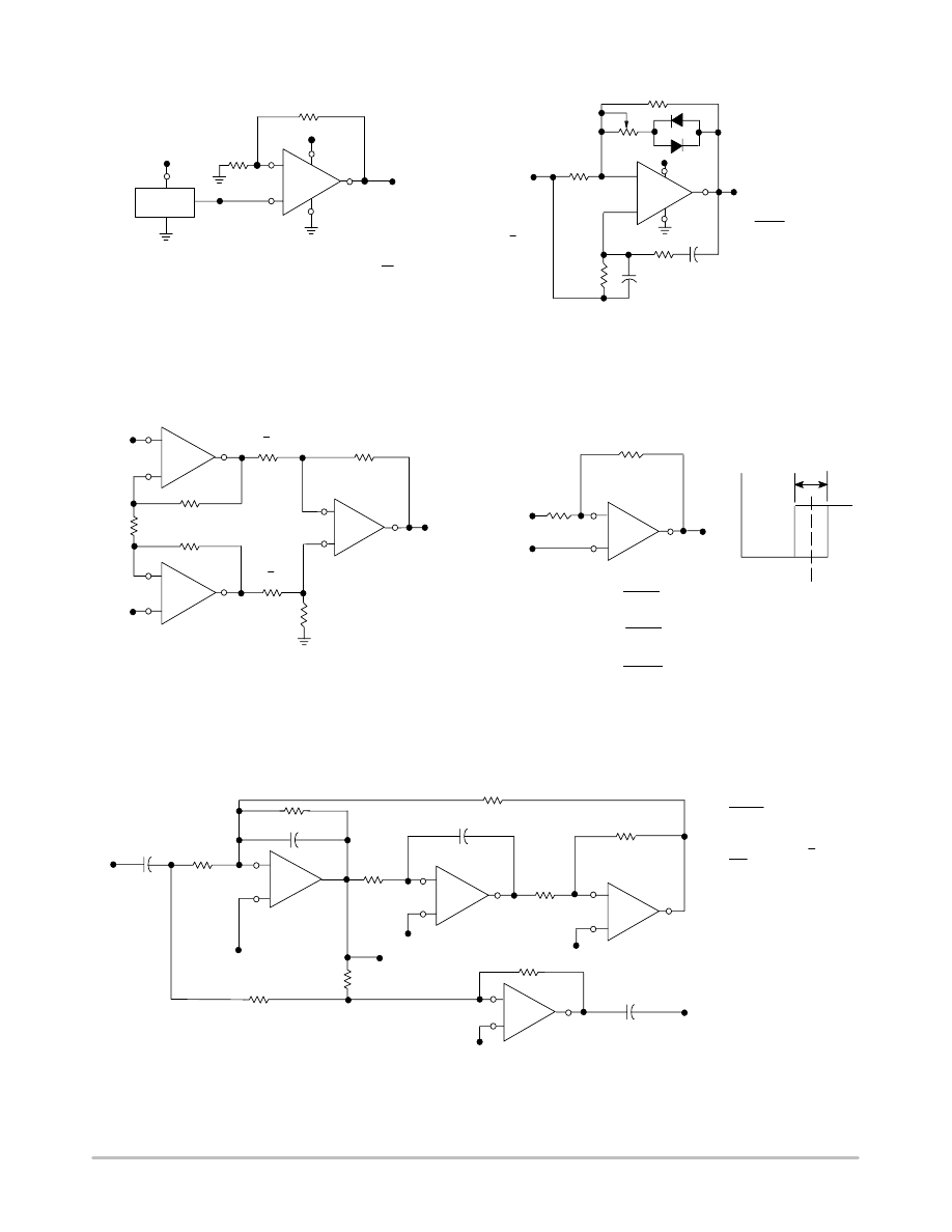
8
R1
2
1
R1
T
BP
R1 + R2
R1
R1 + R2
1
e
o
e
1
e
2
e
o
= C (1 + a + b) (e
2
− e
1
)
R1
a R1
b R1
R
C
R
−
+
1/2
LM358
+
−
−
+
R
1/2
LM358
+
−
R1
R2
V
O
V
ref
V
in
V
OH
V
O
V
OL
V
inL
=
R1
(V
OL
− V
ref
)+ V
ref
V
inH
=
(V
OH
− V
ref
) + V
ref
H =
R1 + R2
(V
OH
− V
OL
)
R1
−
+
−
+
−
+
R
C
R2
R3
C1
100 k
R
C
R
C1
R2
100 k
V
in
V
ref
V
ref
V
ref
V
ref
Bandpass
Output
f
o
=
2
RC
R1 = QR
R2 =
R3 = T
N R2
C1 = 10 C
1
Notch Output
V
ref
=
V
CC
Hysteresis
1/2
LM358
1/2
LM358
1
C
R
V
inL
V
inH
V
ref
1/2
LM358
1/2
LM358
1/2
LM358
1/2
LM358
T
BP
= Center Frequency Gain
T
N
= Passband Notch Gain
R
C
R1
R2
R3
For:
−
+
f
o
Q
T
BP
T
N
= 1.0 kHz
= 10
= 1
= 1
= 160 k
= 0.001
F
= 1.6 M
= 1.6 M
= 1.6 M
Where:
MC1403
1/2
LM358
−
+
R1
V
CC
V
CC
V
O
2.5 V
R2
50 k
10 k
V
ref
V
ref
= V
CC
2
5.0 k
R
C
R
C
+
1/2
LM358
−
V
O
2
RC
1
For: f
o
= 1.0 kHz
R = 16 k
C = 0.01
F
V
O
= 2.5 V (1 +
R1
R2
)
1
V
CC
f
o
=
Figure 10. Voltage Reference
Figure 11. Wien Bridge Oscillator
Figure 12. High Impedance Differential Amplifier
Figure 13. Comparator with Hysteresis
Figure 14. Bi−Quad Filter
LM358, LM258, LM2904, LM2904A, LM2904V, NCV2904
http://onsemi.com
9
2
1
V
ref
=
V
CC
1
2
Figure 15. Function Generator
Figure 16. Multiple Feedback Bandpass Filter
For less than 10% error from operational amplifier.
If source impedance varies, filter may be preceded with voltage
follower buffer to stabilize filter parameters.
Where f
o
and BW are expressed in Hz.
Q
o
f
o
BW
< 0.1
Given:
f
o
= center frequency
A(f
o
) = gain at center frequency
Choose value f
o
, C
Then:
R3 =
Q
f
o
C
R3
R1 =
2 A(f
o
)
R1 R3
4Q
2
R1 −R3
R2 =
+
−
+
−
−
+
V
ref
=
V
CC
V
ref
f =
R1 + R
C
4 CR
f
R1
R3 =
R2 R1
R2 + R1
R2
300 k
75 k
R3
R1
C
Triangle Wave
Output
Square
Wave
Output
V
CC
R3
R1
R2
V
ref
V
in
C
C
V
O
CO
CO = 10 C
R
f
if,
1/2
LM358
V
ref
1/2
LM358
1/2
LM358
100 k
LM358, LM258, LM2904, LM2904A, LM2904V, NCV2904
http://onsemi.com
10
ORDERING INFORMATION
Device
Package
Operating Temperature Range
Shipping
†
LM358D
SOIC−8
0
°
C to +70
°
C
98 Units/Rail
LM358DR2
SOIC−8
2500 Tape & Reel
LM358DR2G
SOIC−8
(Pb−Free)
2500 Tape & Reel
LM358DMR2
Micro8
0
°
C to +70
°
C
4000 Tape & Reel
LM358DMR2G
Micro8
(Pb−Free)
4000 Tape & Reel
LM358N
PDIP−8
0
°
C to +70
°
C
50 Units/Rail
LM358NG
PDIP−8
(Pb−Free)
50 Units/Rail
LM258D
SOIC−8
−25
°
C to +85
°
C
98 Units/Rail
LM258DR2
SOIC−8
2500 Tape & Reel
LM258DMR2
Micro8
4000 Tape & Reel
LM258N
PDIP−8
50 Units/Rail
LM2904D
SOIC−8
−40
°
C to +105
°
C
98 Units/Rail
LM2904DR2
SOIC−8
2500 Tape & Reel
LM2904DMR2
Micro8
2500 Tape & Reel
LM2904N
PDIP−8
−40
°
C to +105
°
C
50 Units/Rail
LM2904ADMR2
Micro8
4000 Tape & Reel
LM2904AN
PDIP−8
50 Units/Rail
LM2904VD
SOIC−8
−40
°
C to +125
°
C
98 Units/Rail
LM2904VDR2
SOIC−8
2500 Tape & Reel
LM2904VDMR2
Micro8
4000 Tape & Reel
LM2904VN
PDIP−8
50 Units/Rail
NCV2904DR2*
SOIC−8
2500 Tape & Reel
NCV2904DMR2*
Micro8
4000 Tape & Reel
*NCV2904 is qualified for automotive use.
†For information on tape and reel specifications, including part orientation and tape sizes, please refer to our Tape and Reel Packaging
Specifications Brochure, BRD8011/D.
LM358, LM258, LM2904, LM2904A, LM2904V, NCV2904
http://onsemi.com
11
PDIP−8
N SUFFIX
CASE 626
SOIC−8
D SUFFIX
CASE 751
MARKING DIAGRAMS
x
= 2 or 3
A
= Assembly Location
WL, L
= Wafer Lot
YY, Y
= Year
WW, W
= Work Week
PDIP−8
AN SUFFIX
CASE 626
SOIC−8
VD SUFFIX
CASE 751
PDIP−8
VN SUFFIX
CASE 626
1
8
LMx58N
AWL
YYWW
1
8
LM2904AN
AWL
YYWW
1
8
LM2904N
AWL
YYWW
1
8
LM2904VN
AWL
YYWW
ALYW
LMx58
1
8
ALYW
2904
1
8
ALYW
2904V
1
8
Micro8
DMR2 SUFFIX
CASE 846A
x58
AYW
1
8
2904
AYW
1
8
904A
AYW
1
8
904V
AYW
1
8
*This diagram also applies to NCV2904
*
*
LM358, LM258, LM2904, LM2904A, LM2904V, NCV2904
http://onsemi.com
12
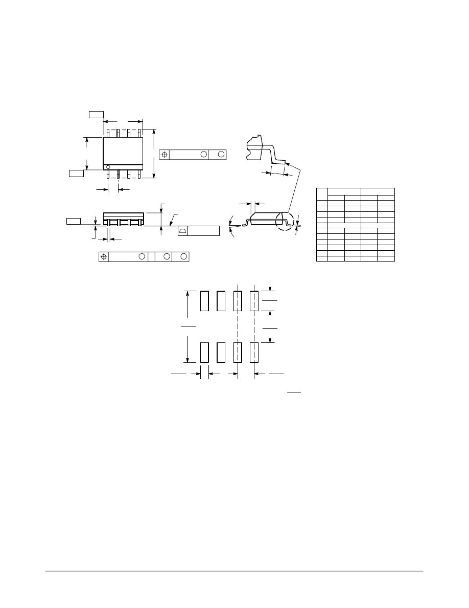
PACKAGE DIMENSIONS
PDIP−8
N, AN, VN SUFFIX
CASE 626−05
ISSUE L
NOTES:
1. DIMENSION L TO CENTER OF LEAD WHEN
FORMED PARALLEL.
2. PACKAGE CONTOUR OPTIONAL (ROUND OR
SQUARE CORNERS).
3. DIMENSIONING AND TOLERANCING PER ANSI
Y14.5M, 1982.
1
4
5
8
F
NOTE 2
−A−
−B−
−T−
SEATING
PLANE
H
J
G
D
K
N
C
L
M
M
A
M
0.13 (0.005)
B
M
T
DIM
MIN
MAX
MIN
MAX
INCHES
MILLIMETERS
A
9.40
10.16
0.370
0.400
B
6.10
6.60
0.240
0.260
C
3.94
4.45
0.155
0.175
D
0.38
0.51
0.015
0.020
F
1.02
1.78
0.040
0.070
G
2.54 BSC
0.100 BSC
H
0.76
1.27
0.030
0.050
J
0.20
0.30
0.008
0.012
K
2.92
3.43
0.115
0.135
L
7.62 BSC
0.300 BSC
M
−−−
10
−−−
10
N
0.76
1.01
0.030
0.040
LM358, LM258, LM2904, LM2904A, LM2904V, NCV2904
http://onsemi.com
13
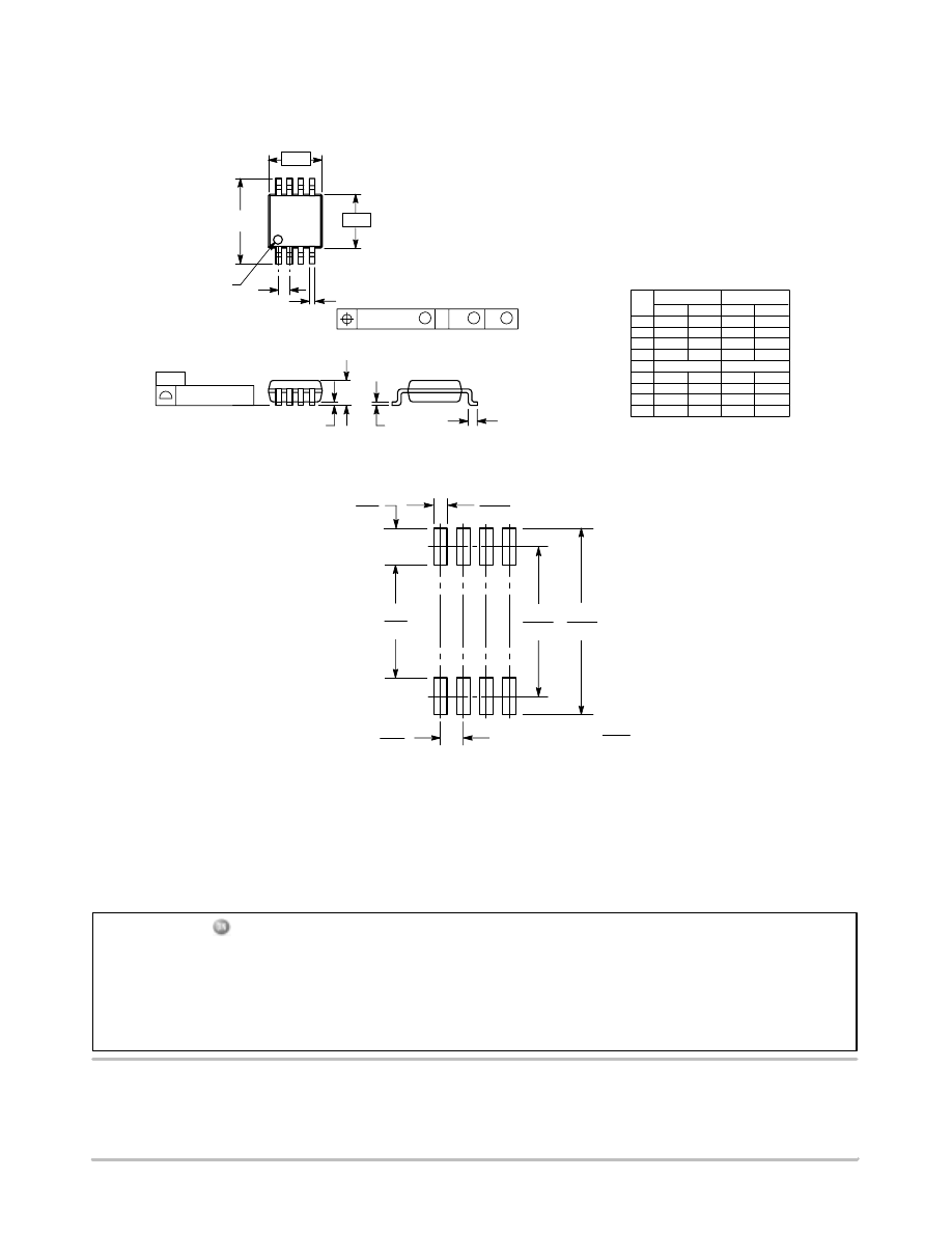
PACKAGE DIMENSIONS
SOIC−8
D, VD SUFFIX
CASE 751−07
ISSUE AA
SEATING
PLANE
1
4
5
8
N
J
X 45
K
NOTES:
1. DIMENSIONING AND TOLERANCING PER ANSI
Y14.5M, 1982.
2. CONTROLLING DIMENSION: MILLIMETER.
3. DIMENSION A AND B DO NOT INCLUDE MOLD
PROTRUSION.
4. MAXIMUM MOLD PROTRUSION 0.15 (0.006) PER
SIDE.
5. DIMENSION D DOES NOT INCLUDE DAMBAR
PROTRUSION. ALLOWABLE DAMBAR
PROTRUSION SHALL BE 0.127 (0.005) TOTAL IN
EXCESS OF THE D DIMENSION AT MAXIMUM
MATERIAL CONDITION.
6. 751−01 THRU 751−06 ARE OBSOLETE. NEW
STANDARD IS 751−07.
A
B
S
D
H
C
0.10 (0.004)
DIM
A
MIN
MAX
MIN
MAX
INCHES
4.80
5.00
0.189
0.197
MILLIMETERS
B
3.80
4.00
0.150
0.157
C
1.35
1.75
0.053
0.069
D
0.33
0.51
0.013
0.020
G
1.27 BSC
0.050 BSC
H
0.10
0.25
0.004
0.010
J
0.19
0.25
0.007
0.010
K
0.40
1.27
0.016
0.050
M
0
8
0
8
N
0.25
0.50
0.010
0.020
S
5.80
6.20
0.228
0.244
−X−
−Y−
G
M
Y
M
0.25 (0.010)
−Z−
Y
M
0.25 (0.010)
Z
S
X
S
M
1.52
0.060
7.0
0.275
0.6
0.024
1.270
0.050
4.0
0.155
mm
inches
SCALE 6:1
*For additional information on our Pb−Free strategy and soldering
details, please download the ON Semiconductor Soldering and
Mounting Techniques Reference Manual, SOLDERRM/D.
SOLDERING FOOTPRINT*
LM358, LM258, LM2904, LM2904A, LM2904V, NCV2904
http://onsemi.com
14
PACKAGE DIMENSIONS
Micro8
DMR2 SUFFIX
CASE 846A−02
ISSUE F
S
B
M
0.08 (0.003)
A
S
T
DIM
MIN
MAX
MIN
MAX
INCHES
MILLIMETERS
A
2.90
3.10
0.114
0.122
B
2.90
3.10
0.114
0.122
C
−−−
1.10
−−−
0.043
D
0.25
0.40
0.010
0.016
G
0.65 BSC
0.026 BSC
H
0.05
0.15
0.002
0.006
J
0.13
0.23
0.005
0.009
K
4.75
5.05
0.187
0.199
L
0.40
0.70
0.016
0.028
NOTES:
1. DIMENSIONING AND TOLERANCING PER ANSI
Y14.5M, 1982.
2. CONTROLLING DIMENSION: MILLIMETER.
3. DIMENSION A DOES NOT INCLUDE MOLD FLASH,
PROTRUSIONS OR GATE BURRS. MOLD FLASH,
PROTRUSIONS OR GATE BURRS SHALL NOT
EXCEED 0.15 (0.006) PER SIDE.
4. DIMENSION B DOES NOT INCLUDE INTERLEAD
FLASH OR PROTRUSION. INTERLEAD FLASH OR
PROTRUSION SHALL NOT EXCEED 0.25 (0.010)
PER SIDE.
5. 846A−01 OBSOLETE, NEW STANDARD 846A−02.
−B−
−A−
D
K
G
PIN 1 ID
8 PL
0.038 (0.0015)
−T−
SEATING
PLANE
C
H
J
L
8X
8X
6X
mm
inches
SCALE 8:1
1.04
0.041
0.38
0.015
5.28
0.208
4.24
0.167
3.20
0.126
0.65
0.0256
*For additional information on our Pb−Free strategy and soldering
details, please download the ON Semiconductor Soldering and
Mounting Techniques Reference Manual, SOLDERRM/D.
SOLDERING FOOTPRINT*
ON Semiconductor and are registered trademarks of Semiconductor Components Industries, LLC (SCILLC). SCILLC reserves the right to make changes without further notice
to any products herein. SCILLC makes no warranty, representation or guarantee regarding the suitability of its products for any particular purpose, nor does SCILLC assume any liability
arising out of the application or use of any product or circuit, and specifically disclaims any and all liability, including without limitation special, consequential or incidental damages.
“Typical” parameters which may be provided in SCILLC data sheets and/or specifications can and do vary in different applications and actual performance may vary over time. All
operating parameters, including “Typicals” must be validated for each customer application by customer’s technical experts. SCILLC does not convey any license under its patent rights
nor the rights of others. SCILLC products are not designed, intended, or authorized for use as components in systems intended for surgical implant into the body, or other applications
intended to support or sustain life, or for any other application in which the failure of the SCILLC product could create a situation where personal injury or death may occur. Should
Buyer purchase or use SCILLC products for any such unintended or unauthorized application, Buyer shall indemnify and hold SCILLC and its officers, employees, subsidiaries, affiliates,
and distributors harmless against all claims, costs, damages, and expenses, and reasonable attorney fees arising out of, directly or indirectly, any claim of personal injury or death
associated with such unintended or unauthorized use, even if such claim alleges that SCILLC was negligent regarding the design or manufacture of the part. SCILLC is an Equal
Opportunity/Affirmative Action Employer. This literature is subject to all applicable copyright laws and is not for resale in any manner.
PUBLICATION ORDERING INFORMATION
N. American Technical Support: 800−282−9855 Toll Free
USA/Canada
Japan: ON Semiconductor, Japan Customer Focus Center
2−9−1 Kamimeguro, Meguro−ku, Tokyo, Japan 153−0051
Phone: 81−3−5773−3850
LM358/D
Micro8 is a trademark of International Rectifier.
LITERATURE FULFILLMENT:
Literature Distribution Center for ON Semiconductor
P.O. Box 5163, Denver, Colorado 80217 USA
Phone: 303−675−2175 or 800−344−3860 Toll Free USA/Canada
Fax: 303−675−2176 or 800−344−3867 Toll Free USA/Canada
Email: orderlit@onsemi.com
ON Semiconductor Website: http://onsemi.com
Order Literature: http://www.onsemi.com/litorder
For additional information, please contact your
local Sales Representative.
Wyszukiwarka
Podobne podstrony:
LM358
LM358
lm358 n
fetch datenblatt lm358
lm358
lm358
LM258 LM358 LM2904 NE532 SA532 SE532
lm358
lm358 2
LM358 2
LM158 LM258 LM358
więcej podobnych podstron