LM158, LM158A, LM258, LM258A
LM358, LM358A, LM358Y, LM2904, LM2904Q
DUAL OPERATIONAL AMPLIFIERS
SLOS068C – JUNE 1976 – REVISED JULY 1998
1
POST OFFICE BOX 655303
•
DALLAS, TEXAS 75265
D
Wide Range of Supply Voltages:
– Single Supply . . . 3 V to 30 V
(LM2904 and LM2904Q . . . 3 V to 26 V) or
– Dual Supplies
D
Low Supply-Current Drain Independent of
Supply Voltage . . . 0.7 mA Typ
D
Common-Mode Input Voltage Range
Includes Ground, Allowing Direct Sensing
Near Ground
D
Low Input Bias and Offset Parameters:
– Input Offset Voltage . . . 3 mV Typ
A Versions . . . 2 mV Typ
– Input Offset Current . . . 2 nA Typ
– Input Bias Current . . . 20 nA Typ
A Versions . . . 15 nA Typ
D
Differential Input Voltage Range Equal to
Maximum-Rated Supply Voltage . . .
±
32 V
(LM2904 and LM2904Q . . .
±
26 V)
D
Open-Loop Differential Voltage
Amplification . . . 100 V/mV Typ
D
Internal Frequency Compensation
description
These devices consist of two independent, high-gain, frequency-compensated operational amplifiers designed
to operate from a single supply over a wide range of voltages. Operation from split supplies also is possible if
the difference between the two supplies is 3 V to 30 V (3 V to 26 V for the LM2904 and LM2904Q), and V
CC
is at least 1.5 V more positive than the input common-mode voltage. The low supply-current drain is independent
of the magnitude of the supply voltage.
Applications include transducer amplifiers, dc amplification blocks, and all the conventional operational
amplifier circuits that now can be more easily implemented in single-supply-voltage systems. For example,
these devices can be operated directly from the standard 5-V supply used in digital systems and easily provides
the required interface electronics without additional
±
5-V supplies.
The LM2904Q is manufactured to demanding automotive requirements.
The LM158 and LM158A are characterized for operation over the full military temperature range of –55
°
C to
125
°
C. The LM258 and LM258A are characterized for operation from –25
°
C to 85
°
C, the LM358 and LM358A
from 0
°
C to 70
°
C, and the LM2904 and LM2904Q from –40
°
C to 125
°
C.
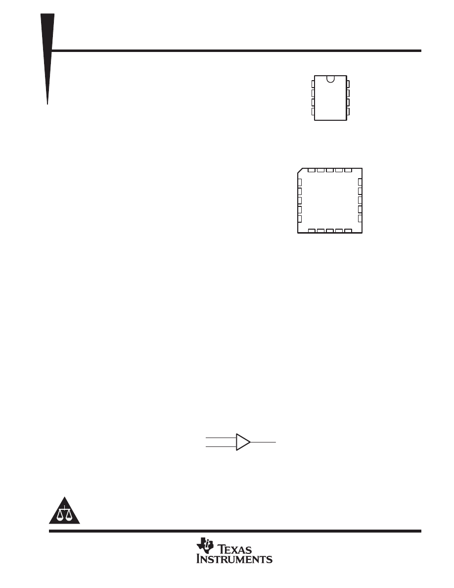
logic diagram (each amplifier)
IN+
IN–
OUT
+
–
Please be aware that an important notice concerning availability, standard warranty, and use in critical applications of
Texas Instruments semiconductor products and disclaimers thereto appears at the end of this data sheet.
Copyright
1998, Texas Instruments Incorporated
PRODUCTION DATA information is current as of publication date.
Products conform to specifications per the terms of Texas Instruments
standard warranty. Production processing does not necessarily include
testing of all parameters.
1
2
3
4
8
7
6
5
1OUT
1IN–
1IN+
GND
V
CC
2OUT
2IN–
2IN+
D, JG, P, OR PW PACKAGE
(TOP VIEW)
3
2 1 20 19
9 10 11 12 13
4
5
6
7
8
18
17
16
15
14
NC
2OUT
NC
2IN–
NC
NC
1IN–
NC
1IN+
NC
LM158, LM158A . . . FK PACKAGE
(TOP VIEW)
NC
1OUT
NC
NC
NC
NC
GND
NC
CC+
V
2IN+
NC – No internal connection
On products compliant to MIL-PRF-38535, all parameters are tested
unless otherwise noted. On all other products, production
processing does not necessarily include testing of all parameters.
LM158, LM158A, LM258, LM258A
LM358, LM358A, LM358Y, LM2904, LM2904Q
DUAL OPERATIONAL AMPLIFIERS
SLOS068C – JUNE 1976 – REVISED JULY 1998
2
POST OFFICE BOX 655303
•
DALLAS, TEXAS 75265
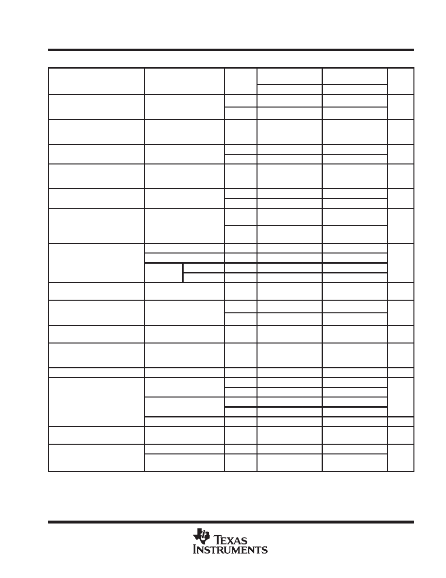
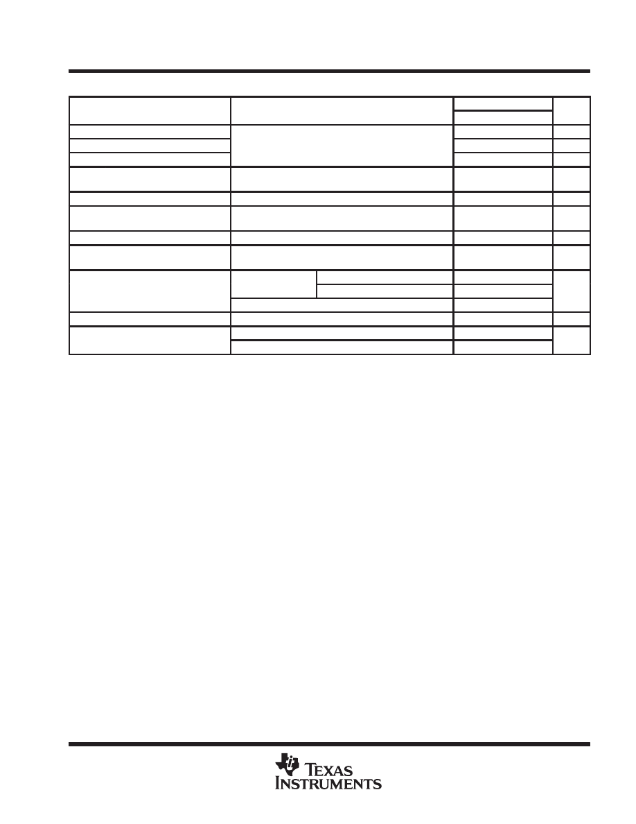
AVAILABLE OPTIONS
PACKAGED DEVICES
CHIP
TA
VIO(max)
AT 25
°
C
SMALL
OUTLINE
(D)†
CHIP
CARRIER
(FK)
CERAMIC
DIP
(JG)
PLASTIC
DIP
(P)
TSSOP
(PW)‡
CHIP
FORM
(Y)
0
°
C to 70
°
C
7 mV
LM358D
—
—
LM358P
LM358PW
LM358Y
0
°
C to 70
°
C
3 mV
—
—
—
LM358AP
—
—
25
°
C to 85
°
C
5 mV
LM258D
—
—
LM258P
—
—
–25
°
C to 85
°
C
3 mV
—
—
—
LM258AP
—
—
40
°
C to 125
°
C
7 mV
LM2904D
—
—
LM2904P
LM2904PW
—
–40
°
C to 125
°
C
7 mV
LM2904QD
—
—
LM2904QP
—
—
55
°
C to 125
°
C
5 mV
LM158D
LM158FK
LM158JG
LM158P
—
—
–55
°
C to 125
°
C
2 mV
—
LM158AFK
LM158AJG
—
—
—
† The D package is available taped and reeled. Add the suffix R to the device type (e.g., LM358DR).
‡ The PW package is only available left-end taped and reeled.
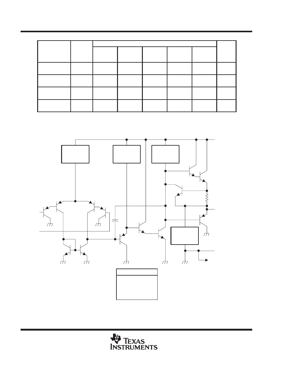
schematic (each amplifier)
VCC+
OUT
GND (or VCC–)
To Other Amplifier
IN–
IN+
≈
6-
µ
A
Current
Regulator
≈
6-
µ
A
Current
Regulator
≈
100-
µ
A
Current
Regulator
≈
50-
µ
A
Current
Regulator
Epi-FET
Diodes
Resistors
Transistors
Capacitors
COMPONENT COUNT
1
2
7
51
2
LM158, LM158A, LM258, LM258A
LM358, LM358A, LM358Y, LM2904, LM2904Q
DUAL OPERATIONAL AMPLIFIERS
SLOS068C – JUNE 1976 – REVISED JULY 1998
3
POST OFFICE BOX 655303
•
DALLAS, TEXAS 75265
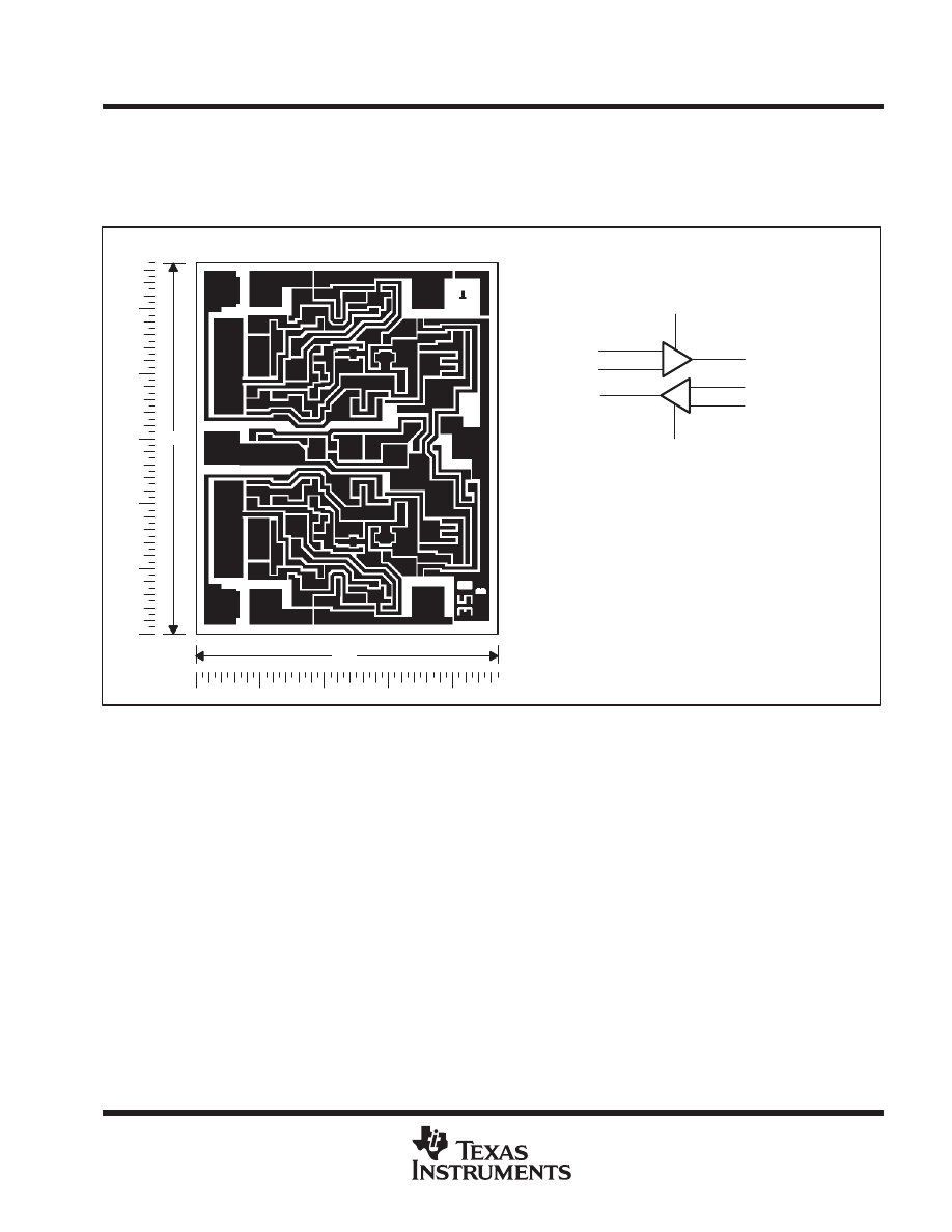
LM358Y chip information
These chips, when properly assembled, display characteristics similar to the LM358. Thermal compression or
ultrasonic bonding can be used on the doped-aluminum bonding pads. Chips can be mounted with conductive
epoxy or a gold-silicon preform.
Chip Thickness: 15 Typical
Bonding Pads: 4
×
4 Minimum
TJ(max) = 150
°
C
Tolerances Are
±
10%.
All Dimensions Are in Mils.
No Backside Metallization
Pin (4) is Internally Connected to Backside of Chip.
BONDING PAD ASSIGNMENTS
47
57
(7)
(6)
(5)
(8)
(4)
(3)
(2)
(1)
1IN+
1IN–
1OUT
+
–
(2)
(3)
(1)
VCC+
(8)
2OUT
2IN+
VCC–
(4)
+
–
2IN–
(5)
(6)
(7)
LM158, LM158A, LM258, LM258A
LM358, LM358A, LM358Y, LM2904, LM2904Q
DUAL OPERATIONAL AMPLIFIERS
SLOS068C – JUNE 1976 – REVISED JULY 1998
4
POST OFFICE BOX 655303
•
DALLAS, TEXAS 75265
absolute maximum ratings over operating free-air temperature range (unless otherwise noted)
LM158, LM158A
LM258, LM258A
LM358, LM358A
LM2904
LM2904Q
UNIT
Supply voltage, VCC (see Note 1)
32
26
V
Differential input voltage, VID (see Note 2)
±
32
±
26
V
Input voltage, VI (either input)
–0.3 to 32
–0.3 to 26
V
Duration of output short circuit (one amplifier) to ground
at (or below) 25
°
C free-air temperature (VCC
≤
15 V) (see Note 3)
Unlimited
Unlimited
Continuous total power dissipation
See Dissipation Rating Table
LM158, LM158A
–55 to 125
Operating free air temperature range TA
LM258, LM258A
–25 to 85
°
C
Operating free-air temperature range, TA
LM358, LM358A
0 to 70
°
C
LM2904, LM2904Q
–40 to 125
Storage temperature range, Tstg
–65 to 150
–65 to 150
°
C
Case temperature for 60 seconds
FK package
260
°
C
Lead temperature 1,6 mm (1/16 inch) from case for 60 seconds
JG package
300
300
°
C
Lead temperature 1,6 mm (1/16 inch) from case for 10 seconds
D, P, or PW package
260
260
°
C
NOTES:
1. All voltage values, except differential voltages and VCC specified for measurement of IOS, are with respect to the network ground
terminal.
2. Differential voltages are at IN+ with respect to IN–.
3. Short circuits from outputs to VCC can cause excessive heating and eventual destruction.
DISSIPATION RATING TABLE
PACKAGE
TA
≤
25
°
C
POWER RATING
DERATING FACTOR
ABOVE TA = 25
°
C
TA = 70
°
C
POWER RATING
TA = 85
°
C
POWER RATING
TA = 125
°
C
POWER RATING
D
725 mW
5.8 mW/
°
C
464 mW
377 mW
145 mW
FK
1375 mW
11.0 mW/
°
C
880 mW
715 mW
275 mW
JG
1050 mW
8.4 mW/
°
C
672 mW
546 mW
210 mW
P
1000 mW
8.0 mW/
°
C
640 mW
520 mW
200 mW
PW
525 mW
4.2 mW/
°
C
336 mW
273 mW
–
LM158, LM158A, LM258, LM258A
LM358, LM358A, LM358Y, LM2904, LM2904Q
DUAL OPERATIONAL AMPLIFIERS
SLOS068C – JUNE 1976 – REVISED JULY 1998
5
POST OFFICE BOX 655303
•
DALLAS, TEXAS 75265
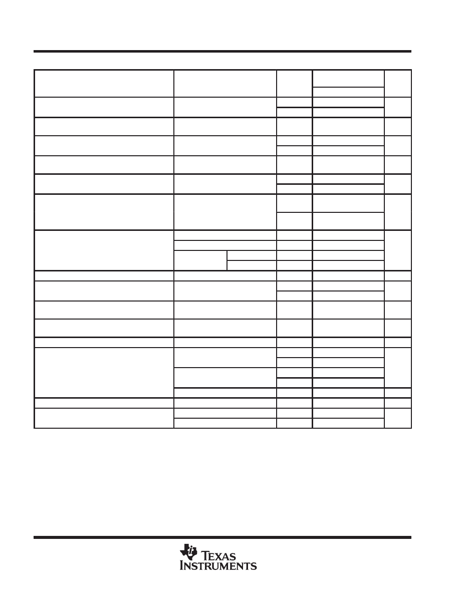
electrical characteristics at specified free-air temperature, V
CC
= 5 V (unless otherwise noted)
PARAMETER
TEST CONDITIONS†
TA‡
LM158
LM258
LM358
UNIT
A
MIN
TYP§
MAX
MIN
TYP§
MAX
VIO
Input offset voltage
VCC = 5 V to MAX,
VIC VICR( i )
25
°
C
3
5
3
7
mV
VIO
Input offset voltage
VIC = VICR(min),
VO = 1.4 V
Full range
7
9
mV
α
VIO
Average temperature
coefficient of
input offset voltage
Full range
7
7
µ
V/
°
C
IIO
Input offset current
VO = 1 4 V
25
°
C
2
30
2
50
nA
IIO
Input offset current
VO = 1.4 V
Full range
100
150
nA
α
IIO
Average temperature
coefficient of
input offset current
Full range
10
10
pA/
°
C
IIB
Input bias current
VO = 1 4 V
25
°
C
–20
–150
–20
–250
nA
IIB
Input bias current
VO = 1.4 V
Full range
–300
–500
nA
VICR
Common-mode
VCC = 5 V to MAX
25
°
C
0 to
VCC–1.5
0 to
VCC–1.5
V
VICR
input voltage range
VCC = 5 V to MAX
Full range
0 to
VCC–2
0 to
VCC–2
V
RL
≥
2 k
Ω
25
°
C
VCC–1.5
VCC–1.5
VOH
High-level
RL
≥
10 k
Ω
25
°
C
V
VOH
g
output voltage
VCC = MAX
RL = 2 k
Ω
Full range
26
26
V
VCC = MAX
RL
≥
10 k
Ω
Full range
27
28
27
28
VOL
Low-level
output voltage
RL
≤
10 k
Ω
Full range
5
20
5
20
mV
AVD
Large-signal
differential
VCC = 15 V,
VO 1 V to 11 V
25
°
C
50
100
25
100
V/mV
AVD
differential
voltage amplification
VO = 1 V to 11 V,
RL =
≥
2 k
Ω
Full range
25
15
V/mV
CMRR
Common-mode
rejection ratio
VCC = 5 V to MAX,
VIC = VICR(min)
25
°
C
70
80
65
80
dB
kSVR
Supply-voltage
rejection ratio
(
∆
VDD/
∆
VIO)
VCC = 5 V to MAX
25
°
C
65
100
65
100
dB
VO1/VO2
Crosstalk attenuation
f = 1 kHz to 20 kHz
25
°
C
120
120
dB
VCC = 15 V, VID = 1 V,
25
°
C
–20
–30
–20
–30
CC
,
ID
,
VO = 0
Full range
–10
–10
mA
IO
Output current
VCC = 15 V, VID = –1 V,
25
°
C
10
20
10
20
mA
CC
,
ID
,
VO = 15 V
Full range
5
5
VID = –1 V,
VO = 200 mV
25
°
C
12
30
12
30
µ
A
IOS
Short-circuit
output current
VCC at 5 V, GND at –5 V,
VO = 0
25
°
C
±
40
±
60
±
40
±
60
mA
Supply current
VO = 2.5 V,
No load
Full range
0.7
1.2
0.7
1.2
ICC
Supply current
(two amplifiers)
VCC = MAX, VO = 0.5 V,
No load
Full range
1
2
1
2
mA
† All characteristics are measured under open-loop conditions with zero common-mode input voltage, unless otherwise specified. MAX VCC for
testing purposes is 26 V for LM 2904 and 30 V for others.
‡ Full range is –55
°
C to 125
°
C for LM158, –25
°
C to 85
°
C for LM258, 0
°
C to 70
°
C for LM358, and –40
°
C to 125
°
C for LM2904 and LM2904Q.
§ All typical values are at TA = 25
°
C.
LM158, LM158A, LM258, LM258A
LM358, LM358A, LM358Y, LM2904, LM2904Q
DUAL OPERATIONAL AMPLIFIERS
SLOS068C – JUNE 1976 – REVISED JULY 1998
6
POST OFFICE BOX 655303
•
DALLAS, TEXAS 75265
electrical characteristics at specified free-air temperature, V
CC
= 5 V (unless otherwise noted)
PARAMETER
TEST CONDITIONS†
TA‡
LM2904
LM2904Q
UNIT
A
MIN
TYP§
MAX
VIO
Input offset voltage
VCC = 5 V to MAX,
25
°
C
3
7
mV
VIO
Input offset voltage
CC
,
VIC = VICR(min), VO = 1.4 V
Full range
10
mV
α
VIO
Average temperature coefficient of
input offset voltage
Full range
7
µ
V/
°
C
IIO
Input offset current
VO = 1 4 V
25
°
C
2
50
nA
IIO
Input offset current
VO = 1.4 V
Full range
300
nA
α
IIO
Average temperature coefficient of
input offset current
Full range
10
pA/
°
C
IIB
Input bias current
VO = 1 4 V
25
°
C
–20
–250
nA
IIB
Input bias current
VO = 1.4 V
Full range
–500
nA
VICR
Common mode input voltage range
VCC = 5 V to MAX
25
°
C
0 to
VCC–1.5
V
VICR
Common-mode input voltage range
VCC = 5 V to MAX
Full range
0 to
VCC–2
V
RL
≥
2 k
Ω
25
°
C
VOH
High level output voltage
RL
≥
10 k
Ω
25
°
C
VCC–1.5
V
VOH
High-level output voltage
VCC = MAX
RL = 2 k
Ω
Full range
26
V
VCC = MAX
RL
≥
10 k
Ω
Full range
23
24
VOL
Low-level output voltage
RL
≤
10 k
Ω
Full range
5
20
mV
AVD
Large-signal differential
VCC = 15 V, VO = 1 V to 11 V,
25
°
C
25
100
V/mV
AVD
g
g
voltage amplification
CC
,
O
,
RL =
≥
2 k
Ω
Full range
15
V/mV
CMRR
Common-mode rejection ratio
VCC = 5 V to MAX,
VIC = VICR(min)
25
°
C
50
80
dB
kSVR
Supply-voltage rejection ratio
(
∆
VDD/
∆
VIO)
VCC = 5 V to MAX
25
°
C
65
100
dB
VO1/VO2
Crosstalk attenuation
f = 1 kHz to 20 kHz
25
°
C
120
dB
VCC = 15 V VID = 1 V VO = 0
25
°
C
–20
–30
VCC = 15 V, VID = 1 V, VO = 0
Full range
–10
mA
IO
Output current
VCC = 15 V VID = 1 V VO = 15 V
25
°
C
10
20
mA
VCC = 15 V, VID = –1 V, VO = 15 V
Full range
5
VID = –1 V,
VO = 200 mV
25
°
C
30
µ
A
IOS
Short-circuit output current
VCC at 5 V, GND at –5 V, VO = 0
25
°
C
±
40
±
60
mA
ICC
Supply current (two amplifiers)
VO = 2.5 V,
No load
Full range
0.7
1.2
mA
ICC
Supply current (two amplifiers)
VCC = MAX, VO = 0.5 V, No load
Full range
1
2
mA
† All characteristics are measured under open-loop conditions with zero common-mode input voltage, unless otherwise specified. MAX VCC for
testing purposes is 26 V for LM 2904 and 30 V for others.
‡ Full range is –55
°
C to 125
°
C for LM158, –25
°
C to 85
°
C for LM258, 0
°
C to 70
°
C for LM358, and –40
°
C to 125
°
C for LM2904 and LM2904Q.
§ All typical values are at TA = 25
°
C.
LM158, LM158A, LM258, LM258A
LM358, LM358A, LM358Y, LM2904, LM2904Q
DUAL OPERATIONAL AMPLIFIERS
SLOS068C – JUNE 1976 – REVISED JULY 1998
7
POST OFFICE BOX 655303
•
DALLAS, TEXAS 75265
electrical characteristics at specified free-air temperature, V
CC
= 5 V (unless otherwise noted)
PARAMETER
TEST CONDITIONS†
T ‡
LM158A
LM258A
UNIT
PARAMETER
TEST CONDITIONS†
TA‡
MIN
TYP§
MAX
MIN
TYP§
MAX
UNIT
VIO
Input offset voltage
VCC = 5 V to 30 V,
VIC VICR( i )
25
°
C
2
2
3
mV
VIO
Input offset voltage
VIC = VICR(min),
VO = 1.4 V
Full range
4
4
mV
α
VIO
Average temperature
coefficient of
input offset voltage
Full range
7
15*
7
15
µ
V/
°
C
IIO
Input offset current
VO = 1 4 V
25
°
C
2
10
2
15
nA
IIO
Input offset current
VO = 1.4 V
Full range
30
30
nA
α
IIO
Average temperature
coefficient of
input offset current
Full range
10
200
10
200
pA/
°
C
IIB
Input bias current
VO = 1 4 V
25
°
C
–15
–50
–15
–80
nA
IIB
Input bias current
VO = 1.4 V
Full range
–100
–100
nA
VICR
Common-mode
VCC = 30 V
25
°
C
0 to
VCC–1.5
0 to
VCC–1.5
V
VICR
input voltage range
VCC = 30 V
Full range
0 to
VCC–2
0 to
VCC–2
V
Hi h l
l
RL
≥
2 k
Ω
25
°
C
VCC–1.5
VCC–1.5
VOH
High-level
output voltage
VCC = 30 V
RL = 2 k
Ω
Full range
26
26
V
out ut voltage
VCC = 30 V
RL
≥
10 k
Ω
Full range
27
28
27
28
VOL
Low-level
output voltage
RL
≤
10 k
Ω
Full range
5
20
5
20
mV
AVD
Large-signal
differential
VCC = 15 V,
VO 1 V to 11 V
25
°
C
50
100
50
100
V/mV
AVD
differential
voltage amplification
VO = 1 V to 11 V,
RL =
≥
2 k
Ω
Full range
25
25
V/mV
CMRR
Common-mode
rejection ratio
25
°
C
70
80
70
80
dB
kSVR
Supply-voltage
rejection ratio
(
∆
VDD/
∆
VIO)
25
°
C
65
100
65
100
dB
VO1/VO2
Crosstalk attenuation
f = 1 kHz to 20 kHz
25
°
C
120
120
dB
*On products compliant to MIL-PRF-38535, this parameter is not production tested.
† All characteristics are measured under open-loop conditions with zero common-mode input voltage, unless otherwise specified.
‡ Full range is –55
°
C to 125
°
C for LM158A, –25
°
C to 85
°
C for LM258A, and 0
°
C to 70
°
C for LM358A.
§ All typical values are at TA = 25
°
C.
LM158, LM158A, LM258, LM258A
LM358, LM358A, LM358Y, LM2904, LM2904Q
DUAL OPERATIONAL AMPLIFIERS
SLOS068C – JUNE 1976 – REVISED JULY 1998
8
POST OFFICE BOX 655303
•
DALLAS, TEXAS 75265
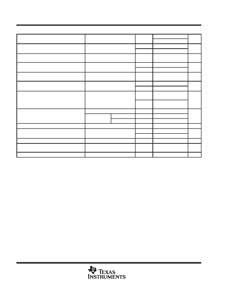
electrical characteristics at specified free-air temperature, V
CC
= 5 V (unless otherwise noted)
PARAMETER
TEST CONDITIONS†
T ‡
LM358A
UNIT
PARAMETER
TEST CONDITIONS†
TA‡
MIN
TYP§
MAX
UNIT
VIO
Input offset voltage
VCC = 5 V to 30 V,
25
°
C
2
3
mV
VIO
Input offset voltage
CC
,
VIC = VICR(min), VO = 1.4 V
Full range
5
mV
α
VIO
Average temperature coefficient of
input offset voltage
Full range
7
20
µ
V/
°
C
IIO
Input offset current
VO = 1 4 V
25
°
C
2
30
nA
IIO
Input offset current
VO = 1.4 V
Full range
75
nA
α
IIO
Average temperature coefficient of
input offset current
Full range
10
300
pA/
°
C
IIB
Input bias current
VO = 1 4 V
25
°
C
–15
–100
nA
IIB
Input bias current
VO = 1.4 V
Full range
–200
nA
VICR
Common mode input voltage range
VCC = 30 V
25
°
C
0 to
VCC–1.5
V
VICR
Common-mode input voltage range
VCC = 30 V
Full range
0 to
VCC–2
V
RL
≥
2 k
Ω
25
°
C
VCC–1.5
VOH
High-level output voltage
VCC = 30 V
RL = 2 k
Ω
Full range
26
V
VCC = 30 V
RL
≥
10 k
Ω
Full range
27
28
VOL
Low-level output voltage
RL
≤
10 k
Ω
Full range
5
20
mV
AVD
Large-signal differential
VCC = 15 V, VO = 1 V to 11 V,
25
°
C
25
100
V/mV
AVD
g
g
voltage amplification
CC
,
O
,
RL =
≥
2 k
Ω
Full range
15
V/mV
CMRR
Common-mode rejection ratio
25
°
C
65
80
dB
kSVR
Supply-voltage rejection ratio
(
∆
VDD/
∆
VIO)
25
°
C
65
100
dB
VO1/VO2
Crosstalk attenuation
f = 1 kHz to 20 kHz
25
°
C
120
dB
† All characteristics are measured under open-loop conditions with zero common-mode input voltage, unless otherwise specified.
‡ Full range is –55
°
C to 125
°
C for LM158A, –25
°
C to 85
°
C for LM258A, and 0
°
C to 70
°
C for LM358A.
§ All typical values are at TA = 25
°
C.
LM158, LM158A, LM258, LM258A
LM358, LM358A, LM358Y, LM2904, LM2904Q
DUAL OPERATIONAL AMPLIFIERS
SLOS068C – JUNE 1976 – REVISED JULY 1998
9
POST OFFICE BOX 655303
•
DALLAS, TEXAS 75265
electrical characteristics V
CC
= 5 V, T
A
=
25
°
C
(unless otherwise noted)
PARAMETER
TEST CONDITIONS†
LM358Y
UNIT
PARAMETER
TEST CONDITIONS†
MIN
TYP
MAX
UNIT
VIO
Input offset voltage
3
7
mV
IIO
Input offset current
VCC = 5 V to MAX,
VIC = VICR(min),
VO = 1.4 V
2
50
nA
IIB
Input bias current
(
)
–20
–250
nA
VICR
Common-mode
input voltage range
VCC = 5 V to MAX
0 to
VCC–1.5
V
VOH+
High-level output voltage
RL
≥
10 k
Ω
VCC–1.5
V
AVD
Large-signal differential
voltage amplification
VCC = 15 V,
VO = 1 V to 11 V,
RL =
≥
2 k
Ω
15
100
V/mV
CMRR
Common-mode rejection ratio
VIC = VICR(min)
65
80
dB
kSVR
Supply-voltage rejection ratio
(
∆
VCC
±
/
∆
VIO)
65
100
dB
VCC = 15 V
VID = 1 V,
VO = 0
–20
–30
–60
IO
Output current
VCC = 15 V
VID = –1 V,
VO = 15 V
10
20
mA
VID = 1 V,
VO = 200 mV
12
30
IOS
Short-circuit output current
VCC at 5 V,
GND at –5 V,
VO = 0
±
40
±
60
mA
ICC
Supply current (four amplifiers)
VO = 2.5 V,
No load
0.7
1.2
mA
ICC
Supply current (four amplifiers)
VCC = MAX,
VO = 0.5 V,
No load
1
2
mA
† All characteristics are measured under open-loop conditions with zero common-mode input voltage, unless otherwise specified. MAX VCC for
testing purposes is 30 V.

IMPORTANT NOTICE
Texas Instruments and its subsidiaries (TI) reserve the right to make changes to their products or to discontinue
any product or service without notice, and advise customers to obtain the latest version of relevant information
to verify, before placing orders, that information being relied on is current and complete. All products are sold
subject to the terms and conditions of sale supplied at the time of order acknowledgement, including those
pertaining to warranty, patent infringement, and limitation of liability.
TI warrants performance of its semiconductor products to the specifications applicable at the time of sale in
accordance with TI’s standard warranty. Testing and other quality control techniques are utilized to the extent
TI deems necessary to support this warranty. Specific testing of all parameters of each device is not necessarily
performed, except those mandated by government requirements.
CERTAIN APPLICATIONS USING SEMICONDUCTOR PRODUCTS MAY INVOLVE POTENTIAL RISKS OF
DEATH, PERSONAL INJURY, OR SEVERE PROPERTY OR ENVIRONMENTAL DAMAGE (“CRITICAL
APPLICATIONS”). TI SEMICONDUCTOR PRODUCTS ARE NOT DESIGNED, AUTHORIZED, OR
WARRANTED TO BE SUITABLE FOR USE IN LIFE-SUPPORT DEVICES OR SYSTEMS OR OTHER
CRITICAL APPLICATIONS. INCLUSION OF TI PRODUCTS IN SUCH APPLICATIONS IS UNDERSTOOD TO
BE FULLY AT THE CUSTOMER’S RISK.
In order to minimize risks associated with the customer’s applications, adequate design and operating
safeguards must be provided by the customer to minimize inherent or procedural hazards.
TI assumes no liability for applications assistance or customer product design. TI does not warrant or represent
that any license, either express or implied, is granted under any patent right, copyright, mask work right, or other
intellectual property right of TI covering or relating to any combination, machine, or process in which such
semiconductor products or services might be or are used. TI’s publication of information regarding any third
party’s products or services does not constitute TI’s approval, warranty or endorsement thereof.
Copyright
1998, Texas Instruments Incorporated
Wyszukiwarka
Podobne podstrony:
LM358
lm358 n
fetch datenblatt lm358
lm358
lm358
LM258 LM358 LM2904 NE532 SA532 SE532
lm358
lm358 2
LM358 2
LM158 LM258 LM358
LM358 D
więcej podobnych podstron