SERVICE
MANUAL
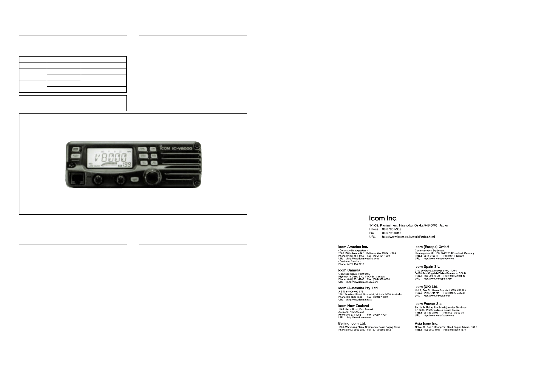
VHF FM TRANSCEIVER
1-1-32, Kamiminami, Hirano-ku, Osaka, 547-0003, Japan
S-13815IZ-C1
© 2002 Icom Inc.
INTRODUCTION
DANGER
This service manual describes the latest service information
for the IC-V8000 VHF FM TRANSCEIVER at the time of pub-
lication.
ORDERING PARTS
Be sure to include the following four points when ordering
replacement parts:
1. 10-digit order numbers
2. Component part number and name
3. Equipment model name and unit name
4. Quantity required
<SAMPLE ORDER>
1110003200 S.IC
TA31136FN
IC-V8000 MAIN UNIT
5 pieces
8810006050 Screw Icom screw E7 IC-V8000 Chassis
10 pieces
Addresses are provided on the inside back cover for your
convenience.
NEVER connect the transceiver to an AC outlet or to a DC
power supply that uses more than 16 V. This will ruin the
transceiver.
DO NOT expose the transceiver to rain, snow or any liquids.
DO NOT reverse the polarities of the power supply when
connecting the transceiver.
DO NOT apply an RF signal of more than 20 dBm (100mW)
to the antenna connector. This could damage the trans-
ceiver's front end.
REPAIR NOTES
1. Make sure a problem is internal before disassembling
the transceiver.
2. DO NOT open the transceiver until the transceiver is dis-
connected from its power source.
3. DO NOT force any of the variable components. Turn
them slowly and smoothly.
4. DO NOT short any circuits or electronic parts. An insulat-
ed turning tool MUST be used for all adjustments.
5. DO NOT keep power ON for a long time when the trans-
ceiver is defective.
6. DO NOT transmit power into a signal generator or a
sweep generator.
7. ALWAYS connect a 50 dB to 60 dB attenuator between
the transceiver and a deviation meter or spectrum ana-
lyzer when using such test equipment.
8. READ the instructions of test equipment thoroughly
before connecting equipment to the transceiver.
To upgrade quality, any electrical or mechanical parts and
internal circuits are subject to change without notice or
obligation.
VERSION
Asia
C.S.America
U.S.A.
SYMBOL
SEA
CSA
CSA-1
USA-2
USA-3
SUPPLIED MICROPHONE
HM-118N
HM-118TN
HM-133V
HM-118TAN

SECTION
1
SPECIFICATIONS
SECTION
2
INSIDE VIEWS
SECTION
3
DISASSEMBLY AND OPTION INSTRUCTIONS
SECTION
4
CIRCUIT DESCRIPTION
4-1
RECEIVER CIRCUITS . . . . . . . . . . . . . . . . . . . . . . . . . . . . . . . . . . . . . . . . . . . . . . . . . . . . .4-1
4-2
TRANSMITTER CIRCUITS . . . . . . . . . . . . . . . . . . . . . . . . . . . . . . . . . . . . . . . . . . . . . . . . . .4-2
4-3
PLL CIRCUITS . . . . . . . . . . . . . . . . . . . . . . . . . . . . . . . . . . . . . . . . . . . . . . . . . . . . . . . . . . .4-3
4-4
POWER SUPPLY CIRCUITS . . . . . . . . . . . . . . . . . . . . . . . . . . . . . . . . . . . . . . . . . . . . . . . .4-3
4-5
PORT ALLOCATIONS . . . . . . . . . . . . . . . . . . . . . . . . . . . . . . . . . . . . . . . . . . . . . . . . . . . . .4-4
SECTION
5
PARTS LIST
SECTION
6
MECHANICAL PARTS AND DISASSEMBLY
6-1
IC-V8000 . . . . . . . . . . . . . . . . . . . . . . . . . . . . . . . . . . . . . . . . . . . . . . . . . . . . . . . . . . . . . . .6-1
6-2
HM-133V . . . . . . . . . . . . . . . . . . . . . . . . . . . . . . . . . . . . . . . . . . . . . . . . . . . . . . . . . . . . . . .6-3
SECTION
7
SEMI-CONDUCTOR INFORMATION
SECTION
8
BOARD LAYOUTS
8-1
HM-133V . . . . . . . . . . . . . . . . . . . . . . . . . . . . . . . . . . . . . . . . . . . . . . . . . . . . . . . . . . . . . . .8-1
8-2
LOGIC BOARD . . . . . . . . . . . . . . . . . . . . . . . . . . . . . . . . . . . . . . . . . . . . . . . . . . . . . . . . . . .8-2
8-3
MAIN UNIT . . . . . . . . . . . . . . . . . . . . . . . . . . . . . . . . . . . . . . . . . . . . . . . . . . . . . . . . . . . . . .8-4
SECTION
9
BLOCK DIAGRAM
SECTION
10
VOLTAGE DIAGRAM
10-1
MAIN UNIT . . . . . . . . . . . . . . . . . . . . . . . . . . . . . . . . . . . . . . . . . . . . . . . . . . . . . . . . . . . . . .10-1
10-2
LOGIC BOARD . . . . . . . . . . . . . . . . . . . . . . . . . . . . . . . . . . . . . . . . . . . . . . . . . . . . . . . . . . .10-2
10-3
HM-133V . . . . . . . . . . . . . . . . . . . . . . . . . . . . . . . . . . . . . . . . . . . . . . . . . . . . . . . . . . . . . . .10-3
TABLE OF CONTENTS
1 - 1
‘
‘
GENERAL
• Frequency coverage
:
*Specifications Guaranteed: 144–148 MHz only
• Type of emission
: FM (F2D / F3E)
• Frequency stability
: ± 10 ppm (–10˚C to +60˚C; +14˚F to +140˚F)
• Tuning steps
: 5, 10, 12.5, 15, 20, 25, 30 or 50 kHz
• Antnna connector
: SO-239 (50
Ω
)
• Power supply requirement
: 13.8 V DC (Operable voltage range: 11.7 to 15.9 V)
(negative ground)
• Number of memory channel
: 207 channels (including 6 scan edges and 1 call channel)
• Call channel
: 1 channel
• Scanning mode
: Full, Program, Priority, Memory, Channel, Skip, Tone, DTCS, Bank and WX
• Current drain (approx.)
:
• Usable temperature range
: –10˚C to +60˚C; +14˚F to +140˚F
• Dimensions (projections not included)
: 150(W)
×
50(H)
×
150(D) mm; 5
29
⁄
32
(W)
×
1
31
⁄
32
(H)
×
5
29
⁄
32
(D) in.
• Weight
: 1.09 kg; 12.3 oz.; 38.4 oz
‘
‘
TRANSMITTER
• RF output power (at 13.8 V DC)
: 75 W / 25 W / 10 W / 5 W (High / Middle High / Middle Low / Low)
• Modulation system
: Variable reactance frequency modulation
• Maximum frequency deviation
: Narrow: ±2.5 kHz*; Wide: ±5.0 kHz
• Spurious emissions
: Less than –60 dB
• Microphone connector
: 8-pins modular (600
Ω
)
‘
‘
RECEIVER
• Receive system
: Double conversion superheterodyne system
• Intermediate frequencies
: 1st
21.7 MHz
2nd
450 kHz
• Sensitivity
: 0.15 µV at 12 dB SINAD (typical)
• Squelch sensitivity
: 0.08 µV at threshold (typical)
• Selectivity
: Narrow; More than ±3.0 kHz at –6 dB, Less than ±9.0 kHz at –55 dB*
Wide; More than ±6.0 kHz at –6 dB, Less than ±14.0 kHz at –60 dB
• Spurious and image rejection
: 60 dB (typical)
• Audio output power (at 7.2 V DC)
: More than 2.0 W at 10% distortion with an 8
Ω
load
• Ext. speaker connector
: 3-conductor 3.5(d) mm (
1
⁄
8
”)/8
Ω
*[USA] version only
All stated specifications are subject to change without notice or obligation.
Transmit
Receiving
SECTION 1
SPECIFICATIONS
Version
[USA]
[SEA]
[CSA]
Receive
136.000–174.000 MHz*
Transmit
144.000–148.000 MHz
140.000–150.000 MHz*
136.000–174.000 MHz*
15 A
9.0 A
6.0 A
5.0 A
1.0 A
0.8 A
High (75 W)
Middle High (25 W)
Middle Low (10 W)
Low (5 W)
Max. audio
Stand-by
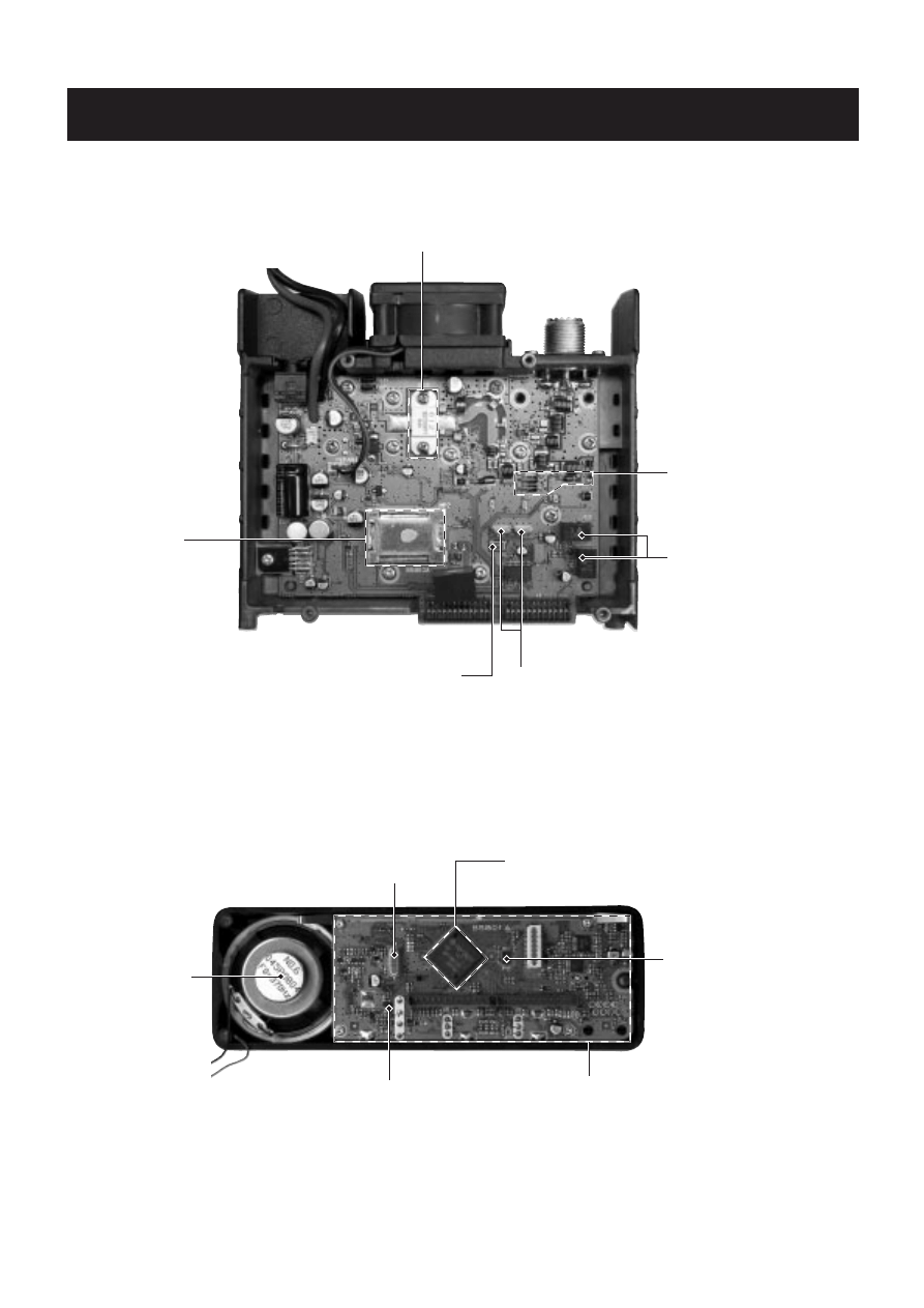
SECTION 2
INSIDE VIEWS
2 - 1
•
MAIN UNIT
•
LOGIC BOARD
Reference oscillator
(X1: CR-659)
VCO circuit
Antenna switching circuit
(D12, D27: XB15A407,
D19: XB15A308,
D16: HVU131TRF)
AF power amplifier
(Q23: RD70HVF1)
1st IF filter
(FI3, FI4: FL-310)
2nd IF filter
(FI1: CFWS450F,
FI2: CFWS450HT)
EEPROM
(IC5: HN58X2432TI)
CPU
(IC7: HD6433876B53H)
System clock
(X1: CR-663)
Speaker
Reset IC
(IC4: S-80942ANMP-DD6)
LOGIC board
SECTION 3
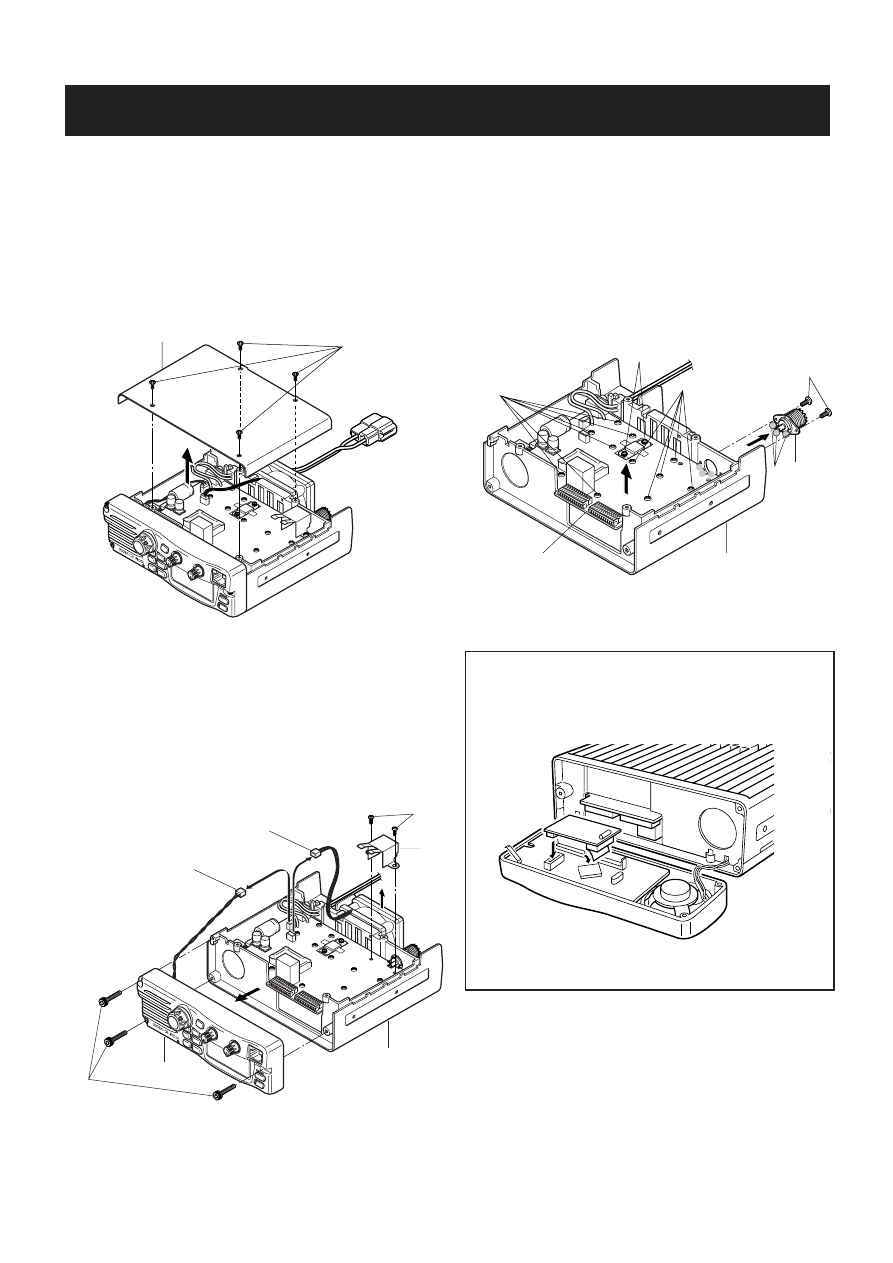
DISASSEMBLY AND OPTION INSTRUCTIONS
3 - 1
Cover
MP10
Front panel
Chassis
MP9
MP6
MP15
J5 (MF1)
J6 (SP7)
Chassis
Main unit
MP6
MP6
MP7
MP4
J1
A
• REMOVING THE COVER
1
Unscrew 4 screws, MP10.
2
Remove the cover in the direction of the arrow.
• REMOVING THE FRONT PANEL
1
Unscrew 3 screws, MP9.
2
Unplug J6 to separate front panel and chassis.
3
Remove the front panel in the direction of the arrow.
4
Unplug J5 to separate fan and chassis.
5
Unscrew 2 screws, MP6, to separate MP15 and chassis.
• REMOVING THE MAIN UNIT
1
Unscrew 11 screws, MP6, and 2 screws, MP7, and 2
screws, MP4.
2
Unsolder 3 points,
A
, to remove the antenna connector.
3
Remove the Main unit in the direction of the arrow.
• OPTIONAL UNIT INSTALLATION
1
Install the optional unit as illustrated below. Insert it tight-
ly to avoid bad contact.
4 - 1
SECTION 4
CIRCUIT DESCRIPTION
4-1
RECEIVER CIRCUITS
4-1-1
ANTENNA SWITCHING CIRCUIT
(MAIN UNIT)
Received signals passed through the low-pass filter (L44,
L47, L48, L51, C190, C197, C203, C208, C210, C217,
C218). The filtered signals are applied to the 1/4
λ
type
antenna switching circuit (D16, D19).
The antenna swtiching circuit functions as a low-pass filter
while transmitting. However, its impedance becomes very
high while D16 and D19 are turn ON. Thus transmit signals
are blocked from entering the receiver circuits. The antenna
switching circuit employs a 1/4
λ
type diode swtiching sys-
tem. The passed signals are then applied to the RF amplifi-
er circuit.
4-1-2
RF CIRCUIT (MAIN UNIT)
The RF circuit amplifies signals within the range of frequen-
cy coverage and filters out-of-band signals.
The signals from the antenna switching circuit are applied to
the limitter (D15), and are then passed through the band-
pass filter (D13, L43, C183, C182). The filtered signals are
amplified at the RF amplifier (Q27), then applied to the 1st
mixer circuit after out-of-band signals are suppressed at the
bandpass filter (D9–D11).
D9–D11, D13 employ varactor diodes that track the band-
pass filters and are controlled by the T1–T3 signals from the
D/A convertor (IC5, pins 10, 11, 23). These diodes tune the
center frequency of an RF passband for wide bandwidth
receiving and good image response rejection.
4-1-3
1ST MIXER AND 1ST IF CIRCUITS
(MAIN UNIT)
The 1st mixer circuit converts the received signal to a fixed
frequency of the 1st IF signal with a PLL output frequency.
By changing the PLL frequency, only the desired frequency
will pass through two crystal filters at the next stage of the
1st mixer.
The signals from the RF circuit are mixed at the 1st mixer
(Q19) with a 1st LO signal coming from the VCO circuit to
produce a 21.70 MHz 1st IF signal.
The 1st IF signal is applied to two crystal filters (FI3 and FI4)
to suppress out-of-band signals. The filtered 1st IF signal is
applied to the IF amplifier (Q16), then applied to the 2nd
mixer circuit (IC4, pin 16).
4-1-4
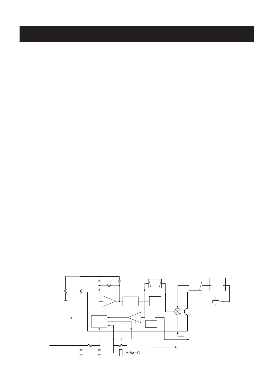
2ND IF AND DEMODULATOR CIRCUITS
(MAIN UNIT)
The 2nd mixer circuit converts the 1st IF signal to a 2nd IF
signal. A double conversion superheterodyne system (which
converts receive signal twice) improves the image rejection
ratio and obtain stable receiver gain.
The 1st IF signal from the IF amplifier is applied to the 2nd
mixer section of the FM IF IC (IC4, pin 16), and is mixed with
the 2nd LO signal to be converted to a 450 kHz 2nd IF sig-
nal.
The FM IF IC contains the 2nd mixer, limiter amplifier, quad-
rature detector and active filter circuits. A 21.25 MHz 2nd LO
signal is produced at the PLL circuit.
The 2nd IF signal from the 2nd mixer (IC4, pin 3) passes
through a ceramic filter (FI1; When wide is selected, F2;
When Narrow is selected. (Narrow is [USA] version only.)) to
remove unwanted heterodyned frequencies. It is then ampli-
fied at the limiter amplifier (IC4, pin 5) and applied to the
quadrature detector (IC4, pins 10, 11) to demodulate the 2nd
IF signal into AF signals.
4-1-5
AF CIRCUIT (MAIN AND LOGIC UNITS)
The AF amplifier circuit amplifies the demodulated AF sig-
nals to drive a speaker.
AF signals from the FM IF IC (IC2, pin 9) are applied to the
analog swtich (LOGIC UNIT; IC6, pin 1) via the high pass fil-
ter (IC3c, pins 9, 8). The output signals from pin 11 are
applied to the volume adjustment pot (LOGIC UNIT; R31).
The signals are applied to the AF power amplifier (IC9, pin
1) after passing through the AFmute swtich (Q29).
Mixer
16
Limiter
amp.
2nd IF filter
450 kHz
PLL IC
IC1
X1
21.25 MHz
IC4 TA31136F
12
1st IF from the IF amplifier (Q16)
"SD" signal to the CPU pin 97
11
10
9
8
7
5
3
AF signal "DETO"
R5V
X2
R55
C84
C85
R64
R59
R71
"SQLIN" signal from the
D/A convertor (IC5, pin 214
R73
C105
C101
C116
2
16
1
Active
filter
FI2
Noise
detector
FM
detector
13
"NOIS" signal to the CPU pin 19
RSSI
Noise
comp.
R63
LPF
• 2ND IF AND DEMODULATOR CIRCUITS
4 - 2
The AF signals are applied to the AF power amplifier circuit
(IC9, pin 1) to obtain the specified audio level. The amplified
AF signals, output from pin 4, are applied to the internal
speaker (CHASSIS UNIT; SP1) via the speaker jack (J6)
when no plug is connected to the external speaker jack (J1).
4-1-6
SQUELCH CIRCUIT
(MAIN AND LOGIC UNITS)
A squelch circuit cuts out AF signals when no RF signals are
received. By detecting noise components in the AF signals,
the squelch switches the analog swtich.
A portion of the AF signals from the FM IF IC (IC4, pin 9) are
applied to the D/A converter (IC5, pin 13) as the DETO sig-
nal. The signals from the D/A converter (IC5, pin 14) are
applied to the FM IF IC active filter section (IC4, pin 8) where
noise components are amplified and detected with an inter-
nal noise detector via the SQLIN line.
The trigger circuit converts the detected signals to a HIGH
or LOW signal and applies this (from pin 13) to the CPU
(LOGIC UNIT; IC7, pin 19) as the NOIS signal.The CPU
controls the analog swtich IC (LOGIC UNIT; IC6) via the
expander IC (LOGIC UNIT; IC8). When the CPU receives a
HIGH level NOIS signal, the CPU controls the RMUT line to
cut the AF signals at the analog swtich IC (LOGIC UNIT;
IC6). At the same time, the AFON line controls the AF mute
circuit (Q29) to cut out the VOLOUT signal for the AF power
amplifier (IC9).
4-2
TRANSMITTER CIRCUITS
4-2-1
MICROPHONE AMPLIFIER CIRCUIT
(LOGIC AND MAIN UNITS)
The microphone amplifier circuit amplifies audio signals with
+6 dB/octave pre-emphasis from the microphone to a level
needed for the modulation circuit.
The AF signals from the microphone pass through the MIC
switch (IC2, D4) and high-pass filter (IC3a, pin 2), and are
then applied to the microphone amplifier circuit (IC3d, pin
12) via the R39 and C47 for +6 dB/octave pre-emphasis.
The amplified AF signals are applied to the analog swtich
(IC6, pin 4), and are then applied to the D/A converter (MAIN
UNIT; IC5, pin 1) via the MODIN signal. The AF signals are
applied to the modulator circuit via the MOD signal.
4-2-2
MODULATION CIRCUIT (MAIN UNIT)
The modulation circuit modulates the VCO oscillating signal
(RF signal) using the microphone audio signals.
The audio signals (SHIFT) change the reactance of D2 to
modulate an oscillated signal at the VCO (Q6, D4). The
oscillated signal is amplified at the LO (Q9) and buffer (Q11)
amplifiers, then applied to the TX/RX switch circuit (D6, D7).
4-2-3
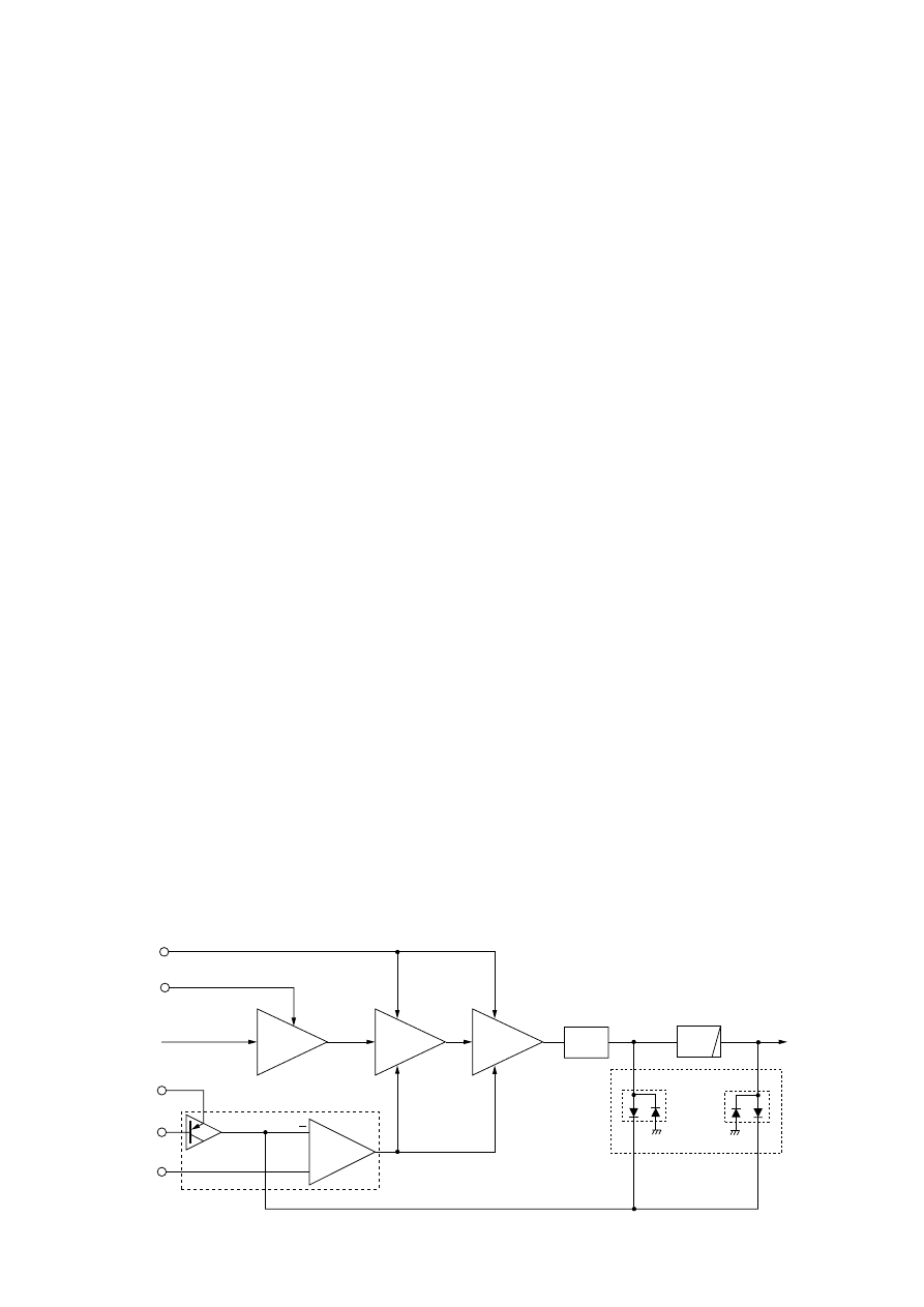
DRIVE/POWER AMPLIFIER CIRCUITS
(MAIN UNIT)
The signal from the VCO circuit passes through the TX/RX
swtiching circuit (D6) and is amplified at the pre-drive (Q17),
drive (Q18, Q20) and power (Q23) amplifiers to obtain 75 W
of RF power (at 13.8 V DC/typical). The amplified signal
passes through the low-pass filter (L37, L39, C151, C156,
C159, C167, C176, C227–C229), and then applied to the
antenna swtiching circuit (D12). The signal is applied to the
antenna connector (CHASSIS UNIT; J1) after being passed
through the low-pass filter (L44, L47, L48, L51, C190, C197,
C203, C208, C210, C217, C218).
The bias current of the drive (Q18, Q20) and power (Q23)
amplifiers is controlled by the APC circuit to stabilize the out-
put power.
4-2-4
APC CIRCUIT (MAIN UNIT)
The APC (Automatic Power Control) circuit (IC6a, Q26) pro-
tects drive and power amplifiers from excessive currents
and selects HIGH or LOW output power.
The output voltage from the power detector circuit (D14,
D17) is applied to the differential amplifier (IC6a, pin 2), and
the “T3” signal from the D/A converter (IC5, pin 23) is
applied to the other input for reference.
When the driving current increases, the input voltage of the
differential amplifier (IC6a, pin 2) will be increased. In such
cases, the differential amplifier output voltage (pin 1) is
decreased to reduce the drive current.
Q26 is controlled by the TXC signal from the expander IC
(IC2, pin 14) to select HIGH or LOW output power.
Q23
Power
amp.
Q20
Driver
amp.
Q18
Driver
amp.
IC6a
+
HV
RF signal from
PLL IC (IC1)
to antenna
T1
TXC
Q26
+5V
APC control circuit
Power detector
circuit (D12, D14)
D14
D12
L44, C190, C191,
C196, C197
LPF
ANT
SW
SWHV
2
3
1
• APC CIRCUIT
4 - 3
4-3
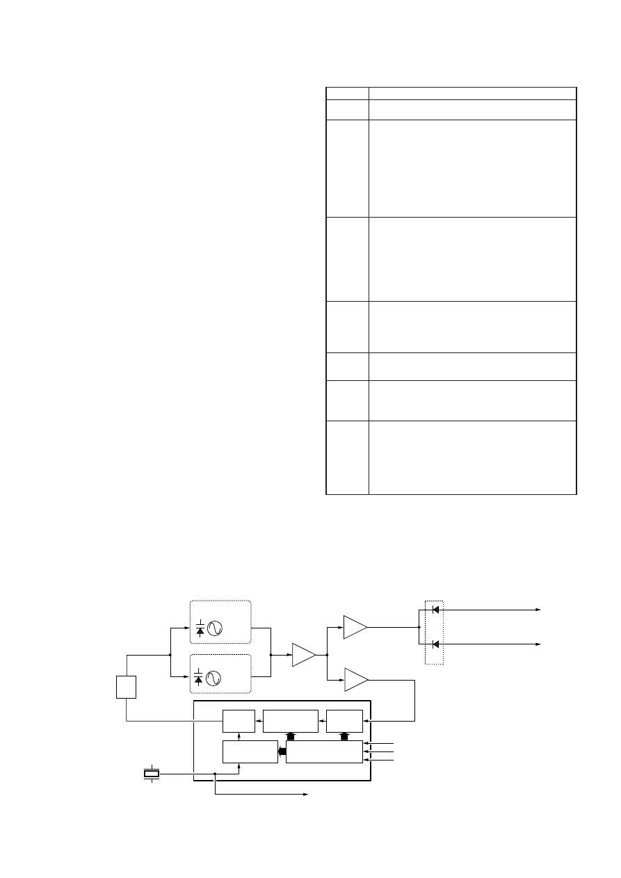
PLL CIRCUITS
4-3-1
PLL CIRCUIT (MAIN AND LOGIC UNITS)
A PLL circuit provides stable oscillation of the transmit fre-
quency and receive 1st LO frequency. The PLL output com-
pares the phase of the divided VCO frequency to the refer-
ence frequency. The PLL output frequency is controlled by
the divided ratio (N-data) of a programmable divider.
An oscillated signal from the TX and RX-VCO circuits pass-
es through the LO and buffer amplifiers (Q9, Q12) is applied
to the PLL IC (IC1, pin 6) and is prescaled in the PLL IC
based on the divided ratio (N-data). The reference signal is
generated at the reference oscillator (X1) and is also applied
to the PLL IC. The PLL IC detects the out-of-step phase
using the reference frequency and outputs it from pin 15.
The output signal is passed through the loop filter(Q2) and
is then applied to the TX and RX-VCO circuits as lock volt-
age.
The lock voltage is also used for the receiver tunable band-
pass filters to match the filter’s center frequency to the
desired receive frequency. The lock voltage is passed
through the loop filter (Q2), and then applied to the DC
amplifier (Q10). The amplified signal is applied to the CPU
(LOGIC unit; IC7, pin 98) via the “LVIN” signal. The signal is
analyzed at the CPU, and then applied to bandpass filters
(D9–D11, D13) as “T1”, “T2”, “T3” signals via the D/A con-
verter.
4-3-2
VCO CIRCUIT (MAIN UNIT)
The VCO circuit contains a separate TX-VCO (Q6, D2, D4)
and RX-VCO (Q7, D5). The oscillated signal is amplified at
the LO (Q9) and buffer (Q11) amplifiers, and is then Tx/Rx
switching circuit (D6, D7). Then Tx and Rx signals are
applied to the pre-driver (Q17) and 1st mixer circuit (Q19)
respectively.
A portion of the signal from LO amplifier (Q9) is amplified at
the buffer amplifier (Q12) and is then fed back to the PLL IC
(IC1, pin 6) as the comparison signal.
Shift register
Prescaler
Phase
detector
Loop
filter
Programable
divider
Reference
divider
X1
25.25 MHz
Q6,
D2,
D4
TX VCO
RX VCO
LO
D7
D6
Q12
Q9
Q2
2
3
4
PLLCK
IC1 (PLL IC)
PLLDATA
PLLSTB
to transmitter circuit
to 1st mixer circuit (Q19)
1
9
6
Q7,
D5
Buff.
Q11
TX/RX
switch
Buff.
25.25 MHz 2nd LO signal
to the 2nd IF IC (IC4, pin 2)
• PLL CIRCUIT
LINE
HV
SWHV
C5V
+8V
+5V
T8
R5V
DESCRIPTION
The voltage from the power supply.
The same voltage as HV line which is controlled
by the HVSW circuit (Q28, Q30, Q31). When the
[POWER] switch is pushed, the CPU outputs the
“PWRON” control signal via the expander IC
(IC2). The signal is applied to the HVSW circuit
to turn the circuit ON.
The output voltage is applied to the drive ampli-
fier (Q18), +8V regulator circuit (IC7), etc.
Common 5 V for the CPU converted from the HV
line by the C5V regulator circuit (IC8). The circuit
outputs the voltage regardless of the power
ON/OFF condition.
The output voltage is applied to the EEPROM
(LOGIC UNIT; IC5), CPU (LOGIC UNIT; IC7),
etc.
Common 8 V converted from the 13.8 V line by
the +8V regulator circuit (IC7).
The output voltage is applied to the LO (Q9) and
buffer (Q11) amplifiers, etc.
Common 5 V converted from the +8 V line by the
+5V regulator circuit (Q21, Q22).
Transmit 8 V controlled by the T8V regulator cir-
cuit (Q14, Q15) using the “TXC” signal from the
I/O expander IC (IC2).
Receive 5 V controlled by the R5V regulator cir-
cuit (Q25) using “RXC” signal from the I/O
expander IC (IC2).
The output voltage is applied to the FM IC IC
(IC4), IF (Q16) and RF (Q27) amplifiers, etc.
4-4
POWER SUPPLY CIRCUITS
VOLTAGE LINE
4 - 4
Pin
Port
Description
number
name
Pin
Port
Description
number
name
4-5
PORT ALLOCATIONS
4-5-1
CPU (LOGIC UNIT: IC7)
1
9
11
12
14
15
16
17
19
20
21
22
23
26
32–35
36–39
40
41
44
45
47
49–51
53
DETO
RESET
CSHIFT
SCK
SO
PTT
CLIN
CLOUT
NOIS
COLOR
DIM1
DIM0
REMO
UNLK
COM4–
COM1
KR3–
KR0
EXTMIC
OPV2
PLLSTB
PLLCK
EXSTB
OPV3
OPT1–
OPT3
DUSE
Input port for the weather alert signal
detection.
Input port for reset signal.
Outputs reference oscillator for the
CPU control signal.
Outputs serial clock signal to the
expander IC (MAIN unit; IC2, pin 3),
D/A convertor IC (MAIN unit, IC5, pin
7), etc.
Outputs serial signals to the D/A con-
vertor IC (MAIN unit; IC5, pin 8),etc.
Input port for the [PTT] switch.
High : While [PTT] switch is pushed.
Input port for the cloning signal.
Outputs the cloning signal.
Input port for noise signals (pulse
type).
Outputs LCD back light color control
signal.
Low : While choosing umber color.
Outputs LCD contrast control signal.
Input port for the remote signals from
a remote microphone (HM-133V) via
the [MIC] jack.
Input port for PLL unlock signal from
the PLL IC (MAIN unit; IC1, pin 14).
Outputs LCD common signals.
Input port for initial matrix.
Low : While keys are pushing.
Input port for the remote control micro-
phone (HM-133V) connecting detec-
tion.
Low : While HM-133V is connected.
Input port for the optional unit detec-
tion signal.
Outputs strobe signals to the PLL IC
(IC1, pin 4).
Outputs PLL IC (IC1, pin 2) clock sig-
nal.
•
Outputs strobe signal to the
expander IC (IC2, pin 1).
• Input port for the optional unit detec-
tion signal.
I/O port for optional unit control signal.
Outputs low-pass filter cut-off frequen-
cy control signal when DTCS is acti-
vated.
54
55
56–88
90
91
95
96
97
98
99
100
Outputs EEPROM (LOGIC unit; IC5,
pin 6) clock signal.
I/O port for the data signals from/to the
EEPROM (LOGIC unit; IC5, pin 5).
Output LCD driver signals.
Outputs CTCSS and DTCS tone sig-
nal.
Outputs DTMF, BEEP and 1750 Hz
tone signal.
Input port for the squelch level detec-
tion.
Input port for the microphone up/down
signal while connecting the micro-
phone.
Input port for the RSSI detection.
Input port for the PLL lock voltage.
Input port for the power detector volt-
age.
Input port for the transceiver’s internal
tempareture detection.
ESCK
ESDA
SEG1–
SEG32
CTCC
TONE
SQLV
MICUD
SD
LVIN
PDET
TEMP
4 - 5
Pin
Port
Description
number
name
2
3
10
11, 23
14
15
22
MOD
SQLATT
T1
T2, T3
SQLIN
DTC
FC
Outputs transmit devetion control sig-
nal.
Outputs attenuator control signal.
• Outputs tunable bandpass filter con-
trol signal while receiving.
• Outputs TX power control signal
while transmitting.
Output tunable bandpass filter control
signals.
Outputs squelch control signal.
Outputs DTCS’s gradient control sig-
nal.
Outputs reference frequency control
signal to X1.
4-5-2
D/A CONVERTOR IC (MAIN UNIT: IC5)
Pin
Port
Description
number
name
4
7
12
6
11
13
14
FANC1
FANC
FANC2
AFMUTE
SHIFT
RXC
TXC
Outputs cooling fan control signal.
The fan speed is depended as shown
below.
Outputs AF mute circuit control signal.
High : While AF mute is ON.
Outputs TX and RX VCO’s regulator
control signals.
High : While receiving.
Low : While transmitting.
Outputs R5 regulator control signal.
Low : While receiving.
Outputs TX power control signal.
High : While transmitting.
4-5-3
I/O EXPANDER IC (MAIN UNIT: IC2)
Fan speed
Hi
Middle
Low
FANC
H
H
H
FANC1
H
L
H
FANC2
H
H
L
S.=Surface mount
IC1
1110002860 S.IC
TA75S393F (TE85R)
IC2
1130004200 S.IC
TC4S66F (TE85R)
IC3
1110005340 S.IC
NJM12902V-TE1
IC4
1130009110 S.IC
S-80942ANMP-DD6-T2
IC5
1130009680 S.IC
HN58X2432TI
IC6
1130008090 S.IC
BU4066BCFV-E1
IC7
1140010400 S.IC
HD6433876B53H (FX-2509A)
IC8
1130007570 S.IC
BU4094BCFV-E2
Q1
1530002690 S.TRANSISTOR 2SC4116-GR (TE85R)
Q2
1590000430 S.TRANSISTOR DTC144EUA T106
Q3
1590001650 S.TRANSISTOR XP4601 (TX)
Q4
1590000430 S.TRANSISTOR DTC144EUA T106
Q5
1590000660 S.TRANSISTOR DTC144TU T106
Q6
1510000510 S.TRANSISTOR 2SA1576A T106R
Q7
1530002690 S.TRANSISTOR 2SC4116-GR (TE85R)
Q8
1530002690 S.TRANSISTOR 2SC4116-GR (TE85R)
Q9
1590000430 S.TRANSISTOR DTC144EUA T106
Q12
1530002690 S.TRANSISTOR 2SC4116-GR (TE85R)
D1
1730002280 S.ZENER
MA8091-M (TX)
D2
1790001250 S.DIODE
MA2S111-(TX)
D3
1730002280 S.ZENER
MA8091-M (TX)
D4
1750000520 S.DIODE
DAN222TL
D6
1750000370 S.DIODE
DA221 TL
D7
1750000520 S.DIODE
DAN222TL
D8
1750000520 S.DIODE
DAN222TL
D9
1750000520 S.DIODE
DAN222TL
D13
1790001250 S.DIODE
MA2S111-(TX)
[SEA], [USA] only
D15
1790001250 S.DIODE
MA2S111-(TX) [USA]
only
D20
1750000520 S.DIODE
DAN222TL
D21
1750000520 S.DIODE
DAN222TL
D22
1790001250 S.DIODE
MA2S111-(TX) [SEA]
only
D23
1790001250 S.DIODE
MA2S111-(TX) [SEA]
only
D24
1790001240 S.DIODE
MA2S728-(TX)
X1
6050010870 S.XTAL
CR-663 (9.200 MHz)
R1
7030004780 S.RESISTOR
ERJ3GEYF 123 V (12 k
Ω
)
R2
7030009550 S.RESISTOR
ERJ3EKF 1203 V (120 k
Ω
)
R3
7030003560 S.RESISTOR
ERJ3GEYJ 103 V (10 k
Ω
)
R4
7030003560 S.RESISTOR
ERJ3GEYJ 103 V (10 k
Ω
)
R5
7030005521 S.RESISTOR
ERA3YKD 334V
R6
7030003680 S.RESISTOR
ERJ3GEYJ 104 V (100 k
Ω
)
R7
7030003320 S.RESISTOR
ERJ3GEYJ 101 V (100
Ω
)
R8
7030003480 S.RESISTOR
ERJ3GEYJ 222 V (2.2 k
Ω
)
R9
7030003600 S.RESISTOR
ERJ3GEYJ 223 V (22 k
Ω
)
R10
7030003560 S.RESISTOR
ERJ3GEYJ 103 V (10 k
Ω
)
R11
7030003680 S.RESISTOR
ERJ3GEYJ 104 V (100 k
Ω
)
R12
7030003680 S.RESISTOR
ERJ3GEYJ 104 V (100 k
Ω
)
R13
7030003450 S.RESISTOR
ERJ3GEYJ 122 V (1.2 k
Ω
)
R14
7030003560 S.RESISTOR
ERJ3GEYJ 103 V (10 k
Ω
)
R15
7030003320 S.RESISTOR
ERJ3GEYJ 101 V (100
Ω
)
R16
7030003660 S.RESISTOR
ERJ3GEYJ 683 V (68 k
Ω
)
R17
7030003660 S.RESISTOR
ERJ3GEYJ 683 V (68 k
Ω
)
R18
7210001860 VARIABLE
EVU-F2AF20 B14 (10KB)
R19
7030003440 S.RESISTOR
ERJ3GEYJ 102 V (1 k
Ω
)
R20
7030003440 S.RESISTOR
ERJ3GEYJ 102 V (1 k
Ω
)
R21
7030003660 S.RESISTOR
ERJ3GEYJ 683 V (68 k
Ω
)
R22
7030003440 S.RESISTOR
ERJ3GEYJ 102 V (1 k
Ω
)
R23
7030003680 S.RESISTOR
ERJ3GEYJ 104 V (100 k
Ω
)
R24
7030003580 S.RESISTOR
ERJ3GEYJ 153 V (15 k
Ω
)
R25
7030003560 S.RESISTOR
ERJ3GEYJ 103 V (10 k
Ω
)
R26
7030003320 S.RESISTOR
ERJ3GEYJ 101 V (100
Ω
)
R27
7030003690 S.RESISTOR
ERJ3GEYJ 124 V (120 k
Ω
)
R28
7030003680 S.RESISTOR
ERJ3GEYJ 104 V (100 k
Ω
)
R29
7030003560 S.RESISTOR
ERJ3GEYJ 103 V (10 k
Ω
)
R30
7030003580 S.RESISTOR
ERJ3GEYJ 153 V (15 k
Ω
)
R31
7210001870 VARIABLE
EVU-F2AF20 A14 (10KA)
R32
7030003450 S.RESISTOR
ERJ3GEYJ 122 V (1.2 k
Ω
)
R34
7030003660 S.RESISTOR
ERJ3GEYJ 683 V (68 k
Ω
)
R35
7030003680 S.RESISTOR
ERJ3GEYJ 104 V (100 k
Ω
)
R36
7030003570 S.RESISTOR
ERJ3GEYJ 123 V (12 k
Ω
)
R37
7030003680 S.RESISTOR
ERJ3GEYJ 104 V (100 k
Ω
)
R38
7030003400 S.RESISTOR
ERJ3GEYJ 471 V (470
Ω
)
R39
7030003700 S.RESISTOR
ERJ3GEYJ 154 V (150 k
Ω
)
R40
7030003640 S.RESISTOR
ERJ3GEYJ 473 V (47 k
Ω
)
R41
7030003570 S.RESISTOR
ERJ3GEYJ 123 V (12 k
Ω
)
R42
7030003800 S.RESISTOR
ERJ3GEYJ 105 V (1 M
Ω
)
R43
7030003800 S.RESISTOR
ERJ3GEYJ 105 V (1 M
Ω
)
R44
7030003800 S.RESISTOR
ERJ3GEYJ 105 V (1 M
Ω
)
R45
7030003510 S.RESISTOR
ERJ3GEYJ 392 V (3.9 k
Ω
)
R46
7410000950 S.ARRAY
EXB-V8V 102JV
R47
7030003680 S.RESISTOR
ERJ3GEYJ 104 V (100 k
Ω
)
R48
7030003800 S.RESISTOR
ERJ3GEYJ 105 V (1 M
Ω
)
R49
7030003610 S.RESISTOR
ERJ3GEYJ 273 V (27 k
Ω
)
R50
7030003800 S.RESISTOR
ERJ3GEYJ 105 V (1 M
Ω
)
R51
7030003200 S.RESISTOR
ERJ3GEYJ 100 V (10
Ω
)
R52
7030003440 S.RESISTOR
ERJ3GEYJ 102 V (1 k
Ω
)
R53
7030003820 S.RESISTOR
ERJ3GEYJ 155 V (1.5 M
Ω
)
R54
7030003440 S.RESISTOR
ERJ3GEYJ 102 V (1 k
Ω
) [USA] only
R55
7030003440 S.RESISTOR
ERJ3GEYJ 102 V (1 k
Ω
)
[SEA], [CSA] only
R56
7030004050 S.RESISTOR
ERJ3GEYJ 1R0 V (1
Ω
)
R57
7030003580 S.RESISTOR
ERJ3GEYJ 153 V (15 k
Ω
)
R58
7030003680 S.RESISTOR
ERJ3GEYJ 104 V (100 k
Ω
)
R59
7030003580 S.RESISTOR
ERJ3GEYJ 153 V (15 k
Ω
)
R60
7030003650 S.RESISTOR
ERJ3GEYJ 563 V (56 k
Ω
)
R61
7030003650 S.RESISTOR
ERJ3GEYJ 563 V (56 k
Ω
)
R62
7030003650 S.RESISTOR
ERJ3GEYJ 563 V (56 k
Ω
)
R64
7030003800 S.RESISTOR
ERJ3GEYJ 105 V (1 M
Ω
)
R67
7030003560 S.RESISTOR
ERJ3GEYJ 103 V (10 k
Ω
)
R69
7030003560 S.RESISTOR
ERJ3GEYJ 103 V (10 k
Ω
)
R70
7030003630 S.RESISTOR
ERJ3GEYJ 393 V (39 k
Ω
)
R71
7030003560 S.RESISTOR
ERJ3GEYJ 103 V (10 k
Ω
)
R72
7030003720 S.RESISTOR
ERJ3GEYJ 224 V (220 k
Ω
)
R73
7030003740 S.RESISTOR
ERJ3GEYJ 334 V (330 k
Ω
)
R74
7030003700 S.RESISTOR
ERJ3GEYJ 154 V (150 k
Ω
)
R75
7030003660 S.RESISTOR
ERJ3GEYJ 683 V (68 k
Ω
)
R76
7030003590 S.RESISTOR
ERJ3GEYJ 183 V (18 k
Ω
)
R77
7030003530 S.RESISTOR
ERJ3GEYJ 562 V (5.6 k
Ω
)
R78
7030003680 S.RESISTOR
ERJ3GEYJ 104 V (100 k
Ω
)
R79
7030003520 S.RESISTOR
ERJ3GEYJ 472 V (4.7 k
Ω
)
R80
7030003440 S.RESISTOR
ERJ3GEYJ 102 V (1 k
Ω
)
R81
7030003690 S.RESISTOR
ERJ3GEYJ 124 V (120 k
Ω
)
R82
7030003440 S.RESISTOR
ERJ3GEYJ 102 V (1 k
Ω
)
R83
7030003300 S.RESISTOR
ERJ3GEYJ 680 V (68
Ω
)
R84
7030003460 S.RESISTOR
ERJ3GEYJ 152 V (1.5 k
Ω
)
R85
7030003550 S.RESISTOR
ERJ3GEYJ 822 V (8.2 k
Ω
)
R86
7030003350 S.RESISTOR
ERJ3GEYJ 181 V (180
Ω
)
R87
7410000950 S.ARRAY
EXB-V8V 102JV
R89
7030003390 S.RESISTOR
ERJ3GEYJ 391 V (390
Ω
)
R91
7030003690 S.RESISTOR
ERJ3GEYJ 124 V (120 k
Ω
)
R92
7030003590 S.RESISTOR
ERJ3GEYJ 183 V (18 k
Ω
)
R93
7030003440 S.RESISTOR
ERJ3GEYJ 102 V (1 k
Ω
)
R94
7030003310 S.RESISTOR
ERJ3GEYJ 820 V (82
Ω
)
R96
7030003630 S.RESISTOR
ERJ3GEYJ 393 V (39 k
Ω
)
R97
7030003340 S.RESISTOR
ERJ3GEYJ 151 V (150
Ω
)
R99
7030003640 S.RESISTOR
ERJ3GEYJ 473 V (47 k
Ω
)
R100
7030003380 S.RESISTOR
ERJ3GEYJ 331 V (330
Ω
)
R101
7030003520 S.RESISTOR
ERJ3GEYJ 472 V (4.7 k
Ω
)
R102
7030003410 S.RESISTOR
ERJ3GEYJ 561 V (560
Ω
)
R103
7030003700 S.RESISTOR
ERJ3GEYJ 154 V (150 k
Ω
)
R104
7030003590 S.RESISTOR
ERJ3GEYJ 183 V (18 k
Ω
)
[SEA], [CSA]
7030003670 S.RESISTOR
ERJ3GEYJ 823 V (82 k
Ω
) [USA]
R105
7030003440 S.RESISTOR
ERJ3GEYJ 102 V (1 k
Ω
)
R106
7030003560 S.RESISTOR
ERJ3GEYJ 103 V (10 k
Ω
)
R107
7030003680 S.RESISTOR
ERJ3GEYJ 104 V (100 k
Ω
)
R108
7030003560 S.RESISTOR
ERJ3GEYJ 103 V (10 k
Ω
)
R109
7030003610 S.RESISTOR
ERJ3GEYJ 273 V (27 k
Ω
)
[USA] only
R110
7030003440 S.RESISTOR
ERJ3GEYJ 102 V (1 k
Ω
)
R111
7030003590 S.RESISTOR
ERJ3GEYJ 183 V (18 k
Ω
)
C1
4030006860 S.CERAMIC
C1608 JB 1H 102K-T-A
C4
4030006860 S.CERAMIC
C1608 JB 1H 102K-T-A
5 - 1
SECTION 5 PARTS LIST
REF
ORDER
DESCRIPTION
NO.
NO.
[LOGIC BOARD]
REF
ORDER
DESCRIPTION
NO.
NO.
[LOGIC BOARD]
5 - 2
S.=Surface mount
C5
4030007090 S.CERAMIC
C1608 CH 1H 470J-T-A
C7
4030006860 S.CERAMIC
C1608 JB 1H 102K-T-A
C8
4030006900 S.CERAMIC
C1608 JB 1H 103K-T-A
C9
4030006860 S.CERAMIC
C1608 JB 1H 102K-T-A
C10
4030006860 S.CERAMIC
C1608 JB 1H 102K-T-A
C11
4030006860 S.CERAMIC
C1608 JB 1H 102K-T-A
C13
4030006860 S.CERAMIC
C1608 JB 1H 102K-T-A
C14
4030006860 S.CERAMIC
C1608 JB 1H 102K-T-A
C15
4030006860 S.CERAMIC
C1608 JB 1H 102K-T-A
C16
4030006860 S.CERAMIC
C1608 JB 1H 102K-T-A
C19
4030006900 S.CERAMIC
C1608 JB 1H 103K-T-A
C20
4030006860 S.CERAMIC
C1608 JB 1H 102K-T-A
C23
4030006860 S.CERAMIC
C1608 JB 1H 102K-T-A
C28
4030006860 S.CERAMIC
C1608 JB 1H 102K-T-A
C30
4030007090 S.CERAMIC
C1608 CH 1H 470J-T-A
C31
4030007090 S.CERAMIC
C1608 CH 1H 470J-T-A
C32
4510004630 S.ELECTROLYTIC ECEV1CA100SR
C33
4030011600 S.CERAMIC
C1608 JB 1E 104K-T-N
C34
4030009880 S.CERAMIC
C1608 JB 1H 682K-T-A
C35
4030008900 S.CERAMIC
C1608 JB 1H 333K-T-A
C36
4030011600 S.CERAMIC
C1608 JB 1E 104K-T-N
C37
4030006900 S.CERAMIC
C1608 JB 1H 103K-T-A
C38
4030009970 S.CERAMIC
C1608 JB 1H 182K-T-A
C39
4030006860 S.CERAMIC
C1608 JB 1H 102K-T-A
C40
4030006860 S.CERAMIC
C1608 JB 1H 102K-T-A
C41
4030011600 S.CERAMIC
C1608 JB 1E 104K-T-N
C42
4030008920 S.CERAMIC
C1608 JB 1H 473K-T-A
C43
4030008920 S.CERAMIC
C1608 JB 1H 473K-T-A
C44
4030008770 S.CERAMIC
C1608 JB 1H 562K-T-A
C45
4030006900 S.CERAMIC
C1608 JB 1H 103K-T-A
C46
4030008880 S.CERAMIC
C1608 JB 1H 223K-T-A
C47
4030011600 S.CERAMIC
C1608 JB 1E 104K-T-N
C48
4030006870 S.CERAMIC
C1608 JB 1H 222K-T-A
C49
4030011600 S.CERAMIC
C1608 JB 1E 104K-T-N
C50
4030007170 S.CERAMIC
C1608 CH 1H 221J-T-A
C51
4030008890 S.CERAMIC
C1608 JB 1H 273K-T-A
C52
4030007090 S.CERAMIC
C1608 CH 1H 470J-T-A
C53
4030007110 S.CERAMIC
C1608 CH 1H 680J-T-A
C54
4030006900 S.CERAMIC
C1608 JB 1H 103K-T-A
C55
4030006950 S.CERAMIC
C1608 CH 1H 040C-T-A
C56
4030006870 S.CERAMIC
C1608 JB 1H 222K-T-A
C57
4030008470 S.CERAMIC
C1608 JB 1H 272K-T-A
C59
4030007030 S.CERAMIC
C1608 CH 1H 150J-T-A
C62
4030006860 S.CERAMIC
C1608 JB 1H 102K-T-A
C64
4030006900 S.CERAMIC
C1608 JB 1H 103K-T-A
C65
4030006900 S.CERAMIC
C1608 JB 1H 103K-T-A
C66
4030006900 S.CERAMIC
C1608 JB 1H 103K-T-A
C67
4510004630 S.ELECTROLYTIC ECEV1CA100SR
C68
4030011600 S.CERAMIC
C1608 JB 1E 104K-T-N
C69
4030011600 S.CERAMIC
C1608 JB 1E 104K-T-N
C70
4030006900 S.CERAMIC
C1608 JB 1H 103K-T-A
C71
4030006900 S.CERAMIC
C1608 JB 1H 103K-T-A
C72
4030008900 S.CERAMIC
C1608 JB 1H 333K-T-A
C73
4510005860 S.ELECTROLYTIC ECEV1HA2R2SR
C74
4030008770 S.CERAMIC
C1608 JB 1H 562K-T-A
C75
4030011280 S.CERAMIC
C1608 CH 1H 271J-T-A
C76
4030008900 S.CERAMIC
C1608 JB 1H 333K-T-A
C77
4510005860 S.ELECTROLYTIC ECEV1HA2R2SR
C78
4030006900 S.CERAMIC
C1608 JB 1H 103K-T-A
C79
4030007170 S.CERAMIC
C1608 CH 1H 221J-T-A
J1
6450002210 CONNECTOR
3017-8821 <AI>
J2
6510020880 CONNECTOR
53244-1217
J3
6510020880 CONNECTOR
53244-1217
J4
6510021970 S.CONNECTOR AXN330C130P
DS1
5040001760 S.LED
SEC 2422C
DS2
5040001760 S.LED
SEC 2422C
DS4
5040001760 S.LED
SEC 2422C
DS5
5040001760 S.LED
SEC 2422C
DS7
5040001760 S.LED
SEC 2422C
DS8
5040001760 S.LED
SEC 2422C
DS10
5040001760 S.LED
SEC 2422C
DS11
5040001760 S.LED
SEC 2422C
DS13
5040002420 S.LED
SML-310MT T86
DS14
5040002420 S.LED
SML-310MT T86
DS16
5040002420 S.LED
SML-310MT T86
DS17
5040002420 S.LED
SML-310MT T86
DS18
5040002420 S.LED
SML-310MT T86
DS19
5030002250 LCD
L1-0256TAM
REF
ORDER
DESCRIPTION
NO.
NO.
[LOGIC BOARD]
S9
2250000370 ENCODER
EVQ-VENF0124B
SP1
2510001150 SPEAKER
045P0804 <KS>
WS1
8600036880
FX2509 P01LO
EP1
6910012350 S.BEAD
MMZ1608Y 102BT
EP2
6910012350 S.BEAD
MMZ1608Y 102BT
EP3
6910012350 S.BEAD
MMZ1608Y 102BT
EP4
6910012350 S.BEAD
MMZ1608Y 102BT
EP5
6910012350 S.BEAD
MMZ1608Y 102BT
EP6
6910012350 S.BEAD
MMZ1608Y 102BT
EP7
6910012350 S.BEAD
MMZ1608Y 102BT
EP8
6910012350 S.BEAD
MMZ1608Y 102BT
EP9
8930057360 LCD CONTACT SRCN-2509-SP-N-W
EP10
0910055312 PCB
B 5801B
IC1
1130008350 S.IC
LV2105V-TLM
IC2
1130007700 S.IC
BU4094BCF-T1
IC4
1110003200 S.IC
TA31136FN (EL)
IC5
1190000350 S.IC
M62363FP-650C
IC6
1110005330 S.IC
NJM12904V-TE1
IC7
1180001250 S.IC
TA7808F (TE16L)
IC8
1180000420 S.IC
TA78L05F (TE12R)
IC9
1110003090 IC
LA4425A
Q1
1530002850 S.TRANSISTOR 2SC4116-BL (TE85R)
Q2
1590001650 S.TRANSISTOR XP4601 (TX)
Q3
1530002850 S.TRANSISTOR 2SC4116-BL (TE85R)
Q4
1530002850 S.TRANSISTOR 2SC4116-BL (TE85R)
Q5
1530002850 S.TRANSISTOR 2SC4116-BL (TE85R)
Q6
1530002920 S.TRANSISTOR 2SC4226-T1 R25
Q7
1530002920 S.TRANSISTOR 2SC4226-T1 R25
Q8
1590001040 S.TRANSISTOR DTA113ZU T106
Q9
1530003220 S.TRANSISTOR 2SC4406-4-TL
Q10
1560000810 S.FET
2SK1069-4-TL
Q11
1530003220 S.TRANSISTOR 2SC4406-4-TL
Q12
1530003220 S.TRANSISTOR 2SC4406-4-TL
Q13
1590000720 S.TRANSISTOR DTA144EUA T106
[USA] only
Q14
1510000690 S.TRANSISTOR 2SA1734 (TE12R)
Q15
1530002850 S.TRANSISTOR 2SC4116-BL (TE85R)
Q16
1530003220 S.TRANSISTOR 2SC4406-4-TL
Q17
1530000370 S.TRANSISTOR 2SC3356-T1B
Q18
1560001100 S.FET
2SK3074 (TE12L)
Q19
1580000660 S.FET
3SK272-(TX)
Q20
1560001060 S.FET
2SK3075 (TE12L)
Q21
1590001010 S.TRANSISTOR DTB113ZK T147
Q22
1590000430 S.TRANSISTOR DTC144EUA T106
Q23
1560001190 FET
RD70HVF
Q25
1590001010 S.TRANSISTOR DTB113ZK T147
Q26
1590000720 S.TRANSISTOR DTA144EUA T106
Q27
1580000660 S.FET
3SK272-(TX)
Q28
1530002970 S.TRANSISTOR 2SC4684 (TE16R)
Q29
1530003090 S.TRANSISTOR 2SC4213-B (TE85R)
Q30
1510000890 S.TRANSISTOR DTA143TU T106
Q31
1590001320 S.TRANSISTOR DTC143ZUA T106
Q32
1530002850 S.TRANSISTOR 2SC4116-BL (TE85R)
Q33
1520000460 S.TRANSISTOR 2SB1132 T100 R
Q34
1530002850 S.TRANSISTOR 2SC4116-BL (TE85R)
D1
1790001250 S.DIODE
MA2S111-(TX)
D2
1750000720 S.VARICAP
HVC375BTRF
D3
1750000770 S.VARICAP
HVC376BTRF
D4
1750000720 S.VARICAP
HVC375BTRF
D5
1750000720 S.VARICAP
HVC375BTRF
D6
1790000620 S.DIODE
MA77 (TX)
D7
1790000620 S.DIODE
MA77 (TX)
D9
1750000710 S.VARICAP
HVC350BTRF
REF
ORDER
DESCRIPTION
NO.
NO.
[LOGIC BOARD]
REF
ORDER
DESCRIPTION
NO.
NO.
[MAIN UNIT]
S.=Surface mount
D10
1750000710 S.VARICAP
HVC350BTRF
D11
1750000710 S.VARICAP
HVC350BTRF
D12
1710001060 DIODE
XB15A407
D13
1750000710 S.VARICAP
HVC350BTRF
D14
1790000980 S.DIODE
MA742 (TX)
D15
1750000550 S.DIODE
1SS355 TE-17
D16
1710000870 S.DIODE
HVU131TRF
D17
1790000980 S.DIODE
MA742 (TX)
D18
1790001250 S.DIODE
MA2S111-(TX)
D19
1710001080 DIODE
XB15A308
D20
1730000520 ZENER
RD20E B2
D21
1790000700 DIODE
DSA3A1
D22
1790001520 S.ZENER
MA8075-L (TX)
D23
1790001250 S.DIODE
MA2S111-(TX) [USA]
only
D24
1790001250 S.DIODE
MA2S111-(TX) [USA]
only
D25
1790001250 S.DIODE
MA2S111-(TX) [USA]
only
D26
1790001250 S.DIODE
MA2S111-(TX) [USA]
only
D27
1710001060 DIODE
XB15A407
D28
1790000980 S.DIODE
MA742 (TX)
D29
1750000370 S.DIODE
DA221 TL
FI1
2020001520 CERAMIC
CFWLA450KFFA-B0 (CFWS450F)
FI2
2020001460 CERAMIC
CFWLA450KHFA-B0 (CFWS450HT)
[USA] only
FI3
2010002420 MONOLITH
21R15AB (FL-310)
FI4
2010002420 MONOLITH
21R15AB (FL-310)
X1
6050010800 S.XTAL
CR-659 (21.25 MHz)
X2
6070000200 DISCRIMINATOR CDBLA450KCAY24-B0
L1
6200004480 S.COIL
MLF1608D R82K-T
L2
6200002850 S.COIL
NL 252018T-R82J
L3
6200001620 S.COIL
ELJFC 1R0K-F
L6
6200009920 S.COIL
C2012C-R10G
L7
6200009910 S.COIL
C6342A-88NG-A
L8
6200004870 S.COIL
ELJFC 2R7K-F
L9
6200004880 S.COIL
ELJFC 3R3K-F
L10
6200001620 S.COIL
ELJFC 1R0K-F
L11
6200006980 S.COIL
ELJRE R10G-F
L12
6200006980 S.COIL
ELJRE R10G-F
L13
6200006980 S.COIL
ELJRE R10G-F
L14
6200006990 S.COIL
ELJRE 56NG-F
L15
6200007000 S.COIL
ELJRE 82NG-F
L18
6200005740 S.COIL
ELJRE 47NG-F
L19
6200004920 S.COIL
MLF1608A 2R2K-T
L20
6200005740 S.COIL
ELJRE 47NG-F
L21
6200006980 S.COIL
ELJRE R10G-F
L22
6200006670 S.COIL
ELJRE 68NG-F
L23
6200005680 S.COIL
ELJRE 15NG-F
L24
6200003590 S.COIL
EXCCL3225U1
L25
6200003280 S.COIL
NL 252018T-2R2J
L26
6200003280 S.COIL
NL 252018T-2R2J
L27
6200003590 S.COIL
EXCCL3225U1
L28
6200008260 S.COIL
0.30-1.7-8TL 60N
L30
6200008490 S.COIL
0.30-0.9-3TR 7.5N
L31
6200009930 S.COIL
C2012C-68NG
L32
6200009930 S.COIL
C2012C-68NG
L33
2040000490 COIL
EXC-ELDR25C
L34
2040000490 COIL
EXC-ELDR25C
L35
6110001680 COIL
LA-254
L37
6200010040 S.COIL
AS100340-10N
L38
6200009920 S.COIL
C2012C-R10G
L39
6200010050 S.COIL
AS080547-47N
L40
6170000180 COIL
LW-19
L42
6200007370 S.COIL
ELJFC R82K-F
L43
6200009750 S.COIL
0.30-2.0-7TL 68N
L44
6200010050 S.COIL
AS080547-47N
L45
6200008150 S.COIL
0.35-1.6-7TL 44N
L46
6200010060 S.COIL
AS080647-56N
L47
6200010070 S.COIL
AS080747-68N
L48
6200010070 S.COIL
AS080747-68N
L50
6200002910 S.COIL
NL 252018T-R27J
L51
6200010050 S.COIL
AS080547-47N
L52
6200002180 S.COIL
NL 252018T-R12J
L53
6200005710 S.COIL
ELJRE 27NG-F
R1
7030003640 S.RESISTOR
ERJ3GEYJ 473 V (47 k
Ω
)
R2
7030003560 S.RESISTOR
ERJ3GEYJ 103 V (10 k
Ω
)
5 - 3
REF
ORDER
DESCRIPTION
NO.
NO.
[MAIN UNIT]
R3
7030003760 S.RESISTOR
ERJ3GEYJ 474 V (470 k
Ω
)
R4
7030003300 S.RESISTOR
ERJ3GEYJ 680 V (68
Ω
)
R5
7030003520 S.RESISTOR
ERJ3GEYJ 472 V (4.7 k
Ω
)
R6
7030003420 S.RESISTOR
ERJ3GEYJ 681 V (680
Ω
)
R7
7510001280 S.THERMISTOR NTCCM20124AG473J-T
R8
7030003680 S.RESISTOR
ERJ3GEYJ 104 V (100 k
Ω
)
R9
7030003560 S.RESISTOR
ERJ3GEYJ 103 V (10 k
Ω
)
R10
7030003640 S.RESISTOR
ERJ3GEYJ 473 V (47 k
Ω
)
R11
7030003560 S.RESISTOR
ERJ3GEYJ 103 V (10 k
Ω
)
R12
7030003320 S.RESISTOR
ERJ3GEYJ 101 V (100
Ω
)
R13
7030003490 S.RESISTOR
ERJ3GEYJ 272 V (2.7 k
Ω
)
R14
7030003800 S.RESISTOR
ERJ3GEYJ 105 V (1 M
Ω
)
R15
7030003730 S.RESISTOR
ERJ3GEYJ 274 V (270 k
Ω
)
R16
7030003600 S.RESISTOR
ERJ3GEYJ 223 V (22 k
Ω
)
R17
7030003720 S.RESISTOR
ERJ3GEYJ 224 V (220 k
Ω
)
R18
7030003440 S.RESISTOR
ERJ3GEYJ 102 V (1 k
Ω
)
R19
7030003550 S.RESISTOR
ERJ3GEYJ 822 V (8.2 k
Ω
)
R20
7030003530 S.RESISTOR
ERJ3GEYJ 562 V (5.6 k
Ω
)
R21
7030003380 S.RESISTOR
ERJ3GEYJ 331 V (330
Ω
)
R22
7030003440 S.RESISTOR
ERJ3GEYJ 102 V (1 k
Ω
)
R23
7030003600 S.RESISTOR
ERJ3GEYJ 223 V (22 k
Ω
)
R24
7030003480 S.RESISTOR
ERJ3GEYJ 222 V (2.2 k
Ω
)
R25
7030003560 S.RESISTOR
ERJ3GEYJ 103 V (10 k
Ω
)
R26
7030003560 S.RESISTOR
ERJ3GEYJ 103 V (10 k
Ω
)
R27
7030003470 S.RESISTOR
ERJ3GEYJ 182 V (1.8 k
Ω
)
R28
7030003440 S.RESISTOR
ERJ3GEYJ 102 V (1 k
Ω
)
R29
7030003560 S.RESISTOR
ERJ3GEYJ 103 V (10 k
Ω
)
R30
7030003490 S.RESISTOR
ERJ3GEYJ 272 V (2.7 k
Ω
)
R31
7030003440 S.RESISTOR
ERJ3GEYJ 102 V (1 k
Ω
)
R32
7030003200 S.RESISTOR
ERJ3GEYJ 100 V (10
Ω
)
R33
7030003200 S.RESISTOR
ERJ3GEYJ 100 V (10
Ω
)
R34
7030003680 S.RESISTOR
ERJ3GEYJ 104 V (100 k
Ω
)
R35
7030003380 S.RESISTOR
ERJ3GEYJ 331 V (330
Ω
)
R36
7030003440 S.RESISTOR
ERJ3GEYJ 102 V (1 k
Ω
)
R37
7030003640 S.RESISTOR
ERJ3GEYJ 473 V (47 k
Ω
)
R39
7030003640 S.RESISTOR
ERJ3GEYJ 473 V (47 k
Ω
)
R40
7030003680 S.RESISTOR
ERJ3GEYJ 104 V (100 k
Ω
)
R41
7030003280 S.RESISTOR
ERJ3GEYJ 470 V (47
Ω
)
R42
7030003400 S.RESISTOR
ERJ3GEYJ 471 V (470
Ω
)
R43
7030003550 S.RESISTOR
ERJ3GEYJ 822 V (8.2 k
Ω
)
R44
7030003320 S.RESISTOR
ERJ3GEYJ 101 V (100
Ω
)
R45
7030003680 S.RESISTOR
ERJ3GEYJ 104 V (100 k
Ω
)
R46
7030003420 S.RESISTOR
ERJ3GEYJ 681 V (680
Ω
)
R47
7030003480 S.RESISTOR
ERJ3GEYJ 222 V (2.2 k
Ω
)
R48
7030003480 S.RESISTOR
ERJ3GEYJ 222 V (2.2 k
Ω
)
R49
7030003520 S.RESISTOR
ERJ3GEYJ 472 V (4.7 k
Ω
)
R50
7030003520 S.RESISTOR
ERJ3GEYJ 472 V (4.7 k
Ω
)
R51
7030003520 S.RESISTOR
ERJ3GEYJ 472 V (4.7 k
Ω
)
R52
7030003460 S.RESISTOR
ERJ3GEYJ 152 V (1.5 k
Ω
)
R54
7030003220 S.RESISTOR
ERJ3GEYJ 150 V (15
Ω
)
R55
7030003640 S.RESISTOR
ERJ3GEYJ 473 V (47 k
Ω
)
R56
7030003400 S.RESISTOR
ERJ3GEYJ 471 V (470
Ω
)
R57
7030003620 S.RESISTOR
ERJ3GEYJ 333 V (33 k
Ω
)
R58
7030003670 S.RESISTOR
ERJ3GEYJ 823 V (82 k
Ω
)
R59
7030003480 S.RESISTOR
ERJ3GEYJ 222 V (2.2 k
Ω
)
R60
7030003260 S.RESISTOR
ERJ3GEYJ 330 V (33
Ω
)
R62
7030003440 S.RESISTOR
ERJ3GEYJ 102 V (1 k
Ω
)
R63
7030003360 S.RESISTOR
ERJ3GEYJ 221 V (220
Ω
)
R64
7030003680 S.RESISTOR
ERJ3GEYJ 104 V (100 k
Ω
)
R66
7030003680 S.RESISTOR
ERJ3GEYJ 104 V (100 k
Ω
)
R67
7030003290 S.RESISTOR
ERJ3GEYJ 560 V (56
Ω
)
R68
7030003720 S.RESISTOR
ERJ3GEYJ 224 V (220 k
Ω
)
R69
7030003620 S.RESISTOR
ERJ3GEYJ 333 V (33 k
Ω
)
R71
7030003400 S.RESISTOR
ERJ3GEYJ 471 V (470
Ω
)
R72
7030003370 S.RESISTOR
ERJ3GEYJ 271 V (270
Ω
)
R73
7030003470 S.RESISTOR
ERJ3GEYJ 182 V (1.8 k
Ω
)
[SEA], [CSA]
7030003510 S.RESISTOR
ERJ3GEYJ 392 V (3.9 k
Ω
) [USA]
R76
7030003320 S.RESISTOR
ERJ3GEYJ 101 V (100
Ω
)
R78
7030003440 S.RESISTOR
ERJ3GEYJ 102 V (1 k
Ω
)
R79
7030003360 S.RESISTOR
ERJ3GEYJ 221 V (220
Ω
)
R81
7030003560 S.RESISTOR
ERJ3GEYJ 103 V (10 k
Ω
)
R82
7030003290 S.RESISTOR
ERJ3GEYJ 560 V (56
Ω
)
R83
7030003620 S.RESISTOR
ERJ3GEYJ 333 V (33 k
Ω
)
R84
7030003560 S.RESISTOR
ERJ3GEYJ 103 V (10 k
Ω
)
R88
7030003400 S.RESISTOR
ERJ3GEYJ 471 V (470
Ω
)
R90
7030003720 S.RESISTOR
ERJ3GEYJ 224 V (220 k
Ω
)
R92
7030003620 S.RESISTOR
ERJ3GEYJ 333 V (33 k
Ω
)
R93
7030003720 S.RESISTOR
ERJ3GEYJ 224 V (220 k
Ω
)
R95
7030000230 S.RESISTOR
MCR10EZHJ 56
Ω
(560)
R96
7030000660 S.RESISTOR
MCR10EZHJ 220 k
Ω
R98
7030009980 S.RESISTOR
ERJ12RSJR15U
REF
ORDER
DESCRIPTION
NO.
NO.
[MAIN UNIT]
5 - 4
S.=Surface mount
R101
7030003720 S.RESISTOR
ERJ3GEYJ 224 V (220 k
Ω
)
R103
7030003680 S.RESISTOR
ERJ3GEYJ 104 V (100 k
Ω
)
R104
7030003740 S.RESISTOR
ERJ3GEYJ 334 V (330 k
Ω
)
R105
7030003680 S.RESISTOR
ERJ3GEYJ 104 V (100 k
Ω
)
R106
7030003560 S.RESISTOR
ERJ3GEYJ 103 V (10 k
Ω
)
R107
7030003710 S.RESISTOR
ERJ3GEYJ 184 V (180 k
Ω
)
R108
7030003480 S.RESISTOR
ERJ3GEYJ 222 V (2.2 k
Ω
)
R109
7030003510 S.RESISTOR
ERJ3GEYJ 392 V (3.9 k
Ω
)
R110
7030003440 S.RESISTOR
ERJ3GEYJ 102 V (1 k
Ω
)
R111
7030003320 S.RESISTOR
ERJ3GEYJ 101 V (100
Ω
)
R112
7030003620 S.RESISTOR
ERJ3GEYJ 333 V (33 k
Ω
)
R113
7030003680 S.RESISTOR
ERJ3GEYJ 104 V (100 k
Ω
)
R114
7030003640 S.RESISTOR
ERJ3GEYJ 473 V (47 k
Ω
)
R117
7030003560 S.RESISTOR
ERJ3GEYJ 103 V (10 k
Ω
)
R118
7030003560 S.RESISTOR
ERJ3GEYJ 103 V (10 k
Ω
)
R119
7030003720 S.RESISTOR
ERJ3GEYJ 224 V (220 k
Ω
)
R120
7030003440 S.RESISTOR
ERJ3GEYJ 102 V (1 k
Ω
)
R121
7030001010 S.RESISTOR
MCR50JZHJ 10
Ω
(100)
R122
7030003640 S.RESISTOR
ERJ3GEYJ 473 V (47 k
Ω
)
R123
7030003540 S.RESISTOR
ERJ3GEYJ 682 V (6.8 k
Ω
)
R124
7030003550 S.RESISTOR
ERJ3GEYJ 822 V (8.2 k
Ω
)
R125
7030000100 S.RESISTOR
MCR10EZHJ 4.7
Ω
(4R7)
R126
7030003550 S.RESISTOR
ERJ3GEYJ 822 V (8.2 k
Ω
)
R127
7030003690 S.RESISTOR
ERJ3GEYJ 124 V (120 k
Ω
)
R128
7030003680 S.RESISTOR
ERJ3GEYJ 104 V (100 k
Ω
)
R129
7030003680 S.RESISTOR
ERJ3GEYJ 104 V (100 k
Ω
)
R130
7030003610 S.RESISTOR
ERJ3GEYJ 273 V (27 k
Ω
)
R131
7030003670 S.RESISTOR
ERJ3GEYJ 823 V (82 k
Ω
)
R132
7030003640 S.RESISTOR
ERJ3GEYJ 473 V (47 k
Ω
)
R133
7030003440 S.RESISTOR
ERJ3GEYJ 102 V (1 k
Ω
)
R134
7030003680 S.RESISTOR
ERJ3GEYJ 104 V (100 k
Ω
)
R135
7030003570 S.RESISTOR
ERJ3GEYJ 123 V (12 k
Ω
)
[USA] only
R136
7030003570 S.RESISTOR
ERJ3GEYJ 123 V (12 k
Ω
)
[USA] only
R137
7030003570 S.RESISTOR
ERJ3GEYJ 123 V (12 k
Ω
)
[USA] only
R138
7030003570 S.RESISTOR
ERJ3GEYJ 123 V (12 k
Ω
)
[USA] only
R139
7030003580 S.RESISTOR
ERJ3GEYJ 153 V (15 k
Ω
)
[USA] only
R140
7030003580 S.RESISTOR
ERJ3GEYJ 153 V (15 k
Ω
)
[USA] only
R150
7030006070 S.RESISTOR
ERJ12YJ101U (100
Ω
)
R151
7030009980 S.RESISTOR
ERJ12RSJR15U
R152
7030003270 S.RESISTOR
ERJ3GEYJ 390 V (39
Ω
)
R153
7030003340 S.RESISTOR
ERJ3GEYJ 151 V (150
Ω
)
R154
7030003340 S.RESISTOR
ERJ3GEYJ 151 V (150
Ω
)
R155
7030003490 S.RESISTOR
ERJ3GEYJ 272 V (2.7 k
Ω
)
[USA] only
R156
7030003640 S.RESISTOR
ERJ3GEYJ 473 V (47 k
Ω
)
[USA] only
R157
7030003640 S.RESISTOR
ERJ3GEYJ 473 V (47 k
Ω
)
[USA] only
R161
7030003620 S.RESISTOR
ERJ3GEYJ 333 V (33 k
Ω
)
R162
7030003610 S.RESISTOR
ERJ3GEYJ 273 V (27 k
Ω
)
R163
7030000230 S.RESISTOR
MCR10EZHJ 56
Ω
(560)
R164
7030000230 S.RESISTOR
MCR10EZHJ 56
Ω
(560)
R165
7030003680 S.RESISTOR
ERJ3GEYJ 104 V (100 k
Ω
)
R166
7030003560 S.RESISTOR
ERJ3GEYJ 103 V (10 k
Ω
)
R167
7030003680 S.RESISTOR
ERJ3GEYJ 104 V (100 k
Ω
)
R168
7030003340 S.RESISTOR
ERJ3GEYJ 151 V (150
Ω
)
R169
7030003270 S.RESISTOR
ERJ3GEYJ 390 V (39
Ω
)
R170
7030003340 S.RESISTOR
ERJ3GEYJ 151 V (150
Ω
)
R171
7030003440 S.RESISTOR
ERJ3GEYJ 102 V (1 k
Ω
) [USA] only
R172
7030003680 S.RESISTOR
ERJ3GEYJ 104 V (100 k
Ω
)
[USA] only
R173
7030003560 S.RESISTOR
ERJ3GEYJ 103 V (10 k
Ω
)
R174
7030003320 S.RESISTOR
ERJ3GEYJ 101 V (100
Ω
)
R175
7030003640 S.RESISTOR
ERJ3GEYJ 473 V (47 k
Ω
)
R176
7030003440 S.RESISTOR
ERJ3GEYJ 102 V (1 k
Ω
)
C1
4550006410 S.TANTALUM
ECST1VY334R
C2
4030006860 S.CERAMIC
C1608 JB 1H 102K-T-A
C3
4510004440 S.ELECTROLYTIC ECEV1HA010SR
C4
4030011600 S.CERAMIC
C1608 JB 1E 104K-T-N
C5
4030006900 S.CERAMIC
C1608 JB 1H 103K-T-A
C7
4030006860 S.CERAMIC
C1608 JB 1H 102K-T-A
C8
4030006860 S.CERAMIC
C1608 JB 1H 102K-T-A
C9
4030006860 S.CERAMIC
C1608 JB 1H 102K-T-A
C10
4510004640 S.ELECTROLYTIC ECEV1CA470SP
REF
ORDER
DESCRIPTION
NO.
NO.
[MAIN UNIT]
C11
4550006250 S.TANTALUM
TEMSVA 1A 106M-8L
C12
4550006760 S.TANTALUM
TEMSVB2 1A 336M-8R
C13
4030007110 S.CERAMIC
C1608 CH 1H 680J-T-A
C14
4030006860 S.CERAMIC
C1608 JB 1H 102K-T-A
C15
4030006860 S.CERAMIC
C1608 JB 1H 102K-T-A
C16
4030006990 S.CERAMIC
C1608 CH 1H 080D-T-A
C17
4030006860 S.CERAMIC
C1608 JB 1H 102K-T-A
C20
4030007090 S.CERAMIC
C1608 CH 1H 470J-T-A
C21
4030007090 S.CERAMIC
C1608 CH 1H 470J-T-A
C22
4030007040 S.CERAMIC
C1608 CH 1H 180J-T-A
C23
4030007070 S.CERAMIC
C1608 CH 1H 330J-T-A
C24
4550006170 S.TANTALUM
ECST1AY225R
C25
4030006980 S.CERAMIC
C1608 CH 1H 070D-T-A
C26
4030007010 S.CERAMIC
C1608 CH 1H 100D-T-A
C28
4030006860 S.CERAMIC
C1608 JB 1H 102K-T-A
C29
4030006980 S.CERAMIC
C1608 CH 1H 070D-T-A
C30
4030006950 S.CERAMIC
C1608 CH 1H 040C-T-A
C31
4030006860 S.CERAMIC
C1608 JB 1H 102K-T-A
C32
4030007020 S.CERAMIC
C1608 CH 1H 120J-T-A
C34
4030009500 S.CERAMIC
C1608 CH 1H 0R5B-T-A
C36
4030006860 S.CERAMIC
C1608 JB 1H 102K-T-A
C37
4030009500 S.CERAMIC
C1608 CH 1H 0R5B-T-A
C38
4030006860 S.CERAMIC
C1608 JB 1H 102K-T-A
C39
4030011600 S.CERAMIC
C1608 JB 1E 104K-T-N
C41
4030006860 S.CERAMIC
C1608 JB 1H 102K-T-A
C42
4030006860 S.CERAMIC
C1608 JB 1H 102K-T-A
C44
4030006860 S.CERAMIC
C1608 JB 1H 102K-T-A
C45
4030006860 S.CERAMIC
C1608 JB 1H 102K-T-A
C47
4030011600 S.CERAMIC
C1608 JB 1E 104K-T-N
C48
4030006860 S.CERAMIC
C1608 JB 1H 102K-T-A
C49
4030007010 S.CERAMIC
C1608 CH 1H 100D-T-A
C50
4030006940 S.CERAMIC
C1608 CH 1H 030C-T-A
C51
4030006860 S.CERAMIC
C1608 JB 1H 102K-T-A
C52
4030006860 S.CERAMIC
C1608 JB 1H 102K-T-A
C53
4030006860 S.CERAMIC
C1608 JB 1H 102K-T-A
C54
4030007050 S.CERAMIC
C1608 CH 1H 220J-T-A
C55
4030007050 S.CERAMIC
C1608 CH 1H 220J-T-A
C56
4030006860 S.CERAMIC
C1608 JB 1H 102K-T-A
C57
4030006860 S.CERAMIC
C1608 JB 1H 102K-T-A
C58
4030006860 S.CERAMIC
C1608 JB 1H 102K-T-A
C59
4030006860 S.CERAMIC
C1608 JB 1H 102K-T-A
C60
4030006860 S.CERAMIC
C1608 JB 1H 102K-T-A
C61
4030007050 S.CERAMIC
C1608 CH 1H 220J-T-A
C62
4030007020 S.CERAMIC
C1608 CH 1H 120J-T-A
C63
4030006860 S.CERAMIC
C1608 JB 1H 102K-T-A
C64
4030011600 S.CERAMIC
C1608 JB 1E 104K-T-N
C65
4030007050 S.CERAMIC
C1608 CH 1H 220J-T-A
C66
4030007050 S.CERAMIC
C1608 CH 1H 220J-T-A
C67
4030006860 S.CERAMIC
C1608 JB 1H 102K-T-A
C68
4030007000 S.CERAMIC
C1608 CH 1H 090D-T-A
C69
4510004630 S.ELECTROLYTIC ECEV1CA100SR
C70
4030006860 S.CERAMIC
C1608 JB 1H 102K-T-A
C71
4030007090 S.CERAMIC
C1608 CH 1H 470J-T-A
C72
4030006860 S.CERAMIC
C1608 JB 1H 102K-T-A
C73
4030007050 S.CERAMIC
C1608 CH 1H 220J-T-A
C74
4030006860 S.CERAMIC
C1608 JB 1H 102K-T-A
C75
4030006860 S.CERAMIC
C1608 JB 1H 102K-T-A
C77
4030006900 S.CERAMIC
C1608 JB 1H 103K-T-A
C78
4030011600 S.CERAMIC
C1608 JB 1E 104K-T-N
C79
4030007080 S.CERAMIC
C1608 CH 1H 390J-T-A
C80
4030007050 S.CERAMIC
C1608 CH 1H 220J-T-A
C81
4030006900 S.CERAMIC
C1608 JB 1H 103K-T-A
C82
4510004630 S.ELECTROLYTIC ECEV1CA100SR
C83
4030012600 S.CERAMIC
C2012 JB 1A 105M-T-A
C84
4030007170 S.CERAMIC
C1608 CH 1H 221J-T-A
C85
4030007170 S.CERAMIC
C1608 CH 1H 221J-T-A
C86
4030006860 S.CERAMIC
C1608 JB 1H 102K-T-A
C87
4030007100 S.CERAMIC
C1608 CH 1H 560J-T-A
C88
4030007100 S.CERAMIC
C1608 CH 1H 560J-T-A
C89
4030006900 S.CERAMIC
C1608 JB 1H 103K-T-A
C90
4030006860 S.CERAMIC
C1608 JB 1H 102K-T-A
C91
4030006860 S.CERAMIC
C1608 JB 1H 102K-T-A
C93
4030006910 S.CERAMIC
C1608 CH 1H 0R5C-T-A
C94
4030006860 S.CERAMIC
C1608 JB 1H 102K-T-A
C95
4030006860 S.CERAMIC
C1608 JB 1H 102K-T-A
C96
4030006860 S.CERAMIC
C1608 JB 1H 102K-T-A
C97
4030006960 S.CERAMIC
C1608 CH 1H 050C-T-A
C98
4030008900 S.CERAMIC
C1608 JB 1H 333K-T-A
C100
4030007120 S.CERAMIC
C1608 CH 1H 820J-T-A
C101
4030006860 S.CERAMIC
C1608 JB 1H 102K-T-A
C102
4030006860 S.CERAMIC
C1608 JB 1H 102K-T-A
C104
4510006220 S.ELECTROLYTIC ECEV1CA101UP
REF
ORDER
DESCRIPTION
NO.
NO.
[MAIN UNIT]

S.=Surface mount
C105
4030006860 S.CERAMIC
C1608 JB 1H 102K-T-A
C106
4030006860 S.CERAMIC
C1608 JB 1H 102K-T-A
C108
4030006860 S.CERAMIC
C1608 JB 1H 102K-T-A
C109
4030006900 S.CERAMIC
C1608 JB 1H 103K-T-A
C111
4030009990 S.CERAMIC
C1608 CH 1H 200J-T-A
C112
4030007100 S.CERAMIC
C1608 CH 1H 560J-T-A
C113
4030006860 S.CERAMIC
C1608 JB 1H 102K-T-A
C116
4030006860 S.CERAMIC
C1608 JB 1H 102K-T-A
C117
4030006900 S.CERAMIC
C1608 JB 1H 103K-T-A
C118
4510004640 S.ELECTROLYTIC ECEV1CA470SP
C120
4030006900 S.CERAMIC
C1608 JB 1H 103K-T-A
C122
4030006860 S.CERAMIC
C1608 JB 1H 102K-T-A
C123
4030006860 S.CERAMIC
C1608 JB 1H 102K-T-A
C124
4030006960 S.CERAMIC
C1608 CH 1H 050C-T-A
C125
4510004630 S.ELECTROLYTIC ECEV1CA100SR
C126
4030006860 S.CERAMIC
C1608 JB 1H 102K-T-A
C127
4030006950 S.CERAMIC
C1608 CH 1H 040C-T-A
C128
4030006860 S.CERAMIC
C1608 JB 1H 102K-T-A
C129
4030006900 S.CERAMIC
C1608 JB 1H 103K-T-A
C130
4030007060 S.CERAMIC
C1608 CH 1H 270J-T-A
C131
4030007080 S.CERAMIC
C1608 CH 1H 390J-T-A
C133
4030006920 S.CERAMIC
C1608 CH 1H 010C-T-A
C134
4030006860 S.CERAMIC
C1608 JB 1H 102K-T-A
C135
4030004990 S.CERAMIC
C2012 CH 1H 101J-T-A
C136
4030006930 S.CERAMIC
C1608 CH 1H 020C-T-A
C137
4030006860 S.CERAMIC
C1608 JB 1H 102K-T-A
C138
4030006860 S.CERAMIC
C1608 JB 1H 102K-T-A
C139
4030007080 S.CERAMIC
C1608 CH 1H 390J-T-A
C140
4030006900 S.CERAMIC
C1608 JB 1H 103K-T-A
C141
4030006960 S.CERAMIC
C1608 CH 1H 050C-T-A
C142
4030006860 S.CERAMIC
C1608 JB 1H 102K-T-A
C145
4030006920 S.CERAMIC
C1608 CH 1H 010C-T-A
C146
4030006860 S.CERAMIC
C1608 JB 1H 102K-T-A
C147
4510006220 S.ELECTROLYTIC ECEV1CA101UP
C148
4030008560 S.CERAMIC
C1608 CH 1H 300J-T-A
C149
4030011600 S.CERAMIC
C1608 JB 1E 104K-T-N
C150
4030006860 S.CERAMIC
C1608 JB 1H 102K-T-A
C151
4030017880 S.CERAMIC
ERF22X 6C2H 560J D01L (GRM111)
C152
4030006930 S.CERAMIC
C1608 CH 1H 020C-T-A
C153
4030011600 S.CERAMIC
C1608 JB 1E 104K-T-N
C154
4030006860 S.CERAMIC
C1608 JB 1H 102K-T-A
C155
4030006900 S.CERAMIC
C1608 JB 1H 103K-T-A
C156
4030017890 S.CERAMIC
ERF22X 6C2H 101J D01L (GRM111)
C157
4550006210 S.TANTALUM
ECST1CX106R
C158
4030006860 S.CERAMIC
C1608 JB 1H 102K-T-A
C159
4030017880 S.CERAMIC
ERF22X 6C2H 560J D01L (GRM111)
C160
4030006860 S.CERAMIC
C1608 JB 1H 102K-T-A
C161
4030006860 S.CERAMIC
C1608 JB 1H 102K-T-A
C163
4030006860 S.CERAMIC
C1608 JB 1H 102K-T-A
C164
4030006860 S.CERAMIC
C1608 JB 1H 102K-T-A
C166
4510006220 S.ELECTROLYTIC ECEV1CA101UP
C167
4030011730 S.CERAMIC
GRM31M2C2H101JV01L (GRM42-6 CH)
C168
4030006860 S.CERAMIC
C1608 JB 1H 102K-T-A
C169
4030006860 S.CERAMIC
C1608 JB 1H 102K-T-A
C170
4030006860 S.CERAMIC
C1608 JB 1H 102K-T-A
C171
4030011160 S.CERAMIC
GRM31M2C2H150JV01L (GRM42-6 CH)
C172
4030006860 S.CERAMIC
C1608 JB 1H 102K-T-A
C173
4030006860 S.CERAMIC
C1608 JB 1H 102K-T-A
C174
4030006860 S.CERAMIC
C1608 JB 1H 102K-T-A
C175
4510006250 S.ELECTROLYTIC ECEV1CA331UP
C176
4030011190 S.CERAMIC
GRM31M2C2H270JV01L (GRM42-6 CH)
C177
4510004630 S.ELECTROLYTIC ECEV1CA100SR
C178
4030006960 S.CERAMIC
C1608 CH 1H 050C-T-A
C179
4030006860 S.CERAMIC
C1608 JB 1H 102K-T-A
C180
4030006860 S.CERAMIC
C1608 JB 1H 102K-T-A
C181
4510004440 S.ELECTROLYTIC ECEV1HA010SR
C182
4030007080 S.CERAMIC
C1608 CH 1H 390J-T-A
C183
4030006920 S.CERAMIC
C1608 CH 1H 010C-T-A
C184
4030006960 S.CERAMIC
C1608 CH 1H 050C-T-A
C185
4030006860 S.CERAMIC
C1608 JB 1H 102K-T-A
C187
4030006860 S.CERAMIC
C1608 JB 1H 102K-T-A
C188
4510004440 S.ELECTROLYTIC ECEV1HA010SR
C189
4030006860 S.CERAMIC
C1608 JB 1H 102K-T-A
C190
4030011020 S.CERAMIC
GRM31M4C2H1R0CY21L (GRM42-6 CK)
C191
4030007020 S.CERAMIC
C1608 CH 1H 120J-T-A
C192
4030008880 S.CERAMIC
C1608 JB 1H 223K-T-A
C193
4030006860 S.CERAMIC
C1608 JB 1H 102K-T-A
C194
4510006250 S.ELECTROLYTIC ECEV1CA331UP
C195
4030008960 S.CERAMIC
C2012 JB 1C 104K-T-A
C196
4030011020 S.CERAMIC
GRM31M4C2H1R0CY21L (GRM42-6 CK)
C197
4030007020 S.CERAMIC
C1608 CH 1H 120J-T-A
C198
4030006860 S.CERAMIC
C1608 JB 1H 102K-T-A
5 - 5
REF
ORDER
DESCRIPTION
NO.
NO.
[MAIN UNIT]
C200
4030006860 S.CERAMIC
C1608 JB 1H 102K-T-A
C201
4030007040 S.CERAMIC
C1608 CH 1H 180J-T-A
C203
4030017980 S.CERAMIC
ERF22X 6C2H 470J D01L
C204
4510006260 S.ELECTROLYTIC ECEV1AA471UP
C205
4030006860 S.CERAMIC
C1608 JB 1H 102K-T-A
C206
4030011050 S.CERAMIC
GRM31M3C2H3R0CY21L (GRM42-6 CJ)
C207
4510006020 ELECTROLYTIC 16 MV 2200 HC
C208
4030011210 S.CERAMIC
GRM31M2C2H330JV01L (GRM42-6 CH)
C209
4030011600 S.CERAMIC
C1608 JB 1E 104K-T-N
C210
4030011160 S.CERAMIC
GRM31M2C2H150JV01L (GRM42-6 CH)
C211
4030006860 S.CERAMIC
C1608 JB 1H 102K-T-A
C212
4030006860 S.CERAMIC
C1608 JB 1H 102K-T-A
C213
4030006860 S.CERAMIC
C1608 JB 1H 102K-T-A
C214
4510004640 S.ELECTROLYTIC ECEV1CA470SP
C215
4030011600 S.CERAMIC
C1608 JB 1E 104K-T-N
C216
4030011600 S.CERAMIC
C1608 JB 1E 104K-T-N
C217
4030011240 S.CERAMIC
GRM31M2C2H470JV01L (GRM42-6 CH)
C218
4030011180 S.CERAMIC
GRM31M2C2H220JV01L (GRM42-6 CH)
C219
4030007000 S.CERAMIC
C1608 CH 1H 090D-T-A
C222
4030006900 S.CERAMIC
C1608 JB 1H 103K-T-A
C224
4030011600 S.CERAMIC
C1608 JB 1E 104K-T-N
C225
4030017200 S.CERAMIC
GRM31BR32J102KY01L (GHM1030 R)
C227
4030011730 S.CERAMIC
GRM31M2C2H101JV01L (GRM42-6 CH)
C228
4030011230 S.CERAMIC
GRM31M2C2H390JV01L (GRM42-6 CH)
C229
4030011230 S.CERAMIC
GRM31M2C2H390JV01L (GRM42-6 CH)
C230
4510004630 S.ELECTROLYTIC ECEV1CA100SR
[USA] only
C232
4030006860 S.CERAMIC
C1608 JB 1H 102K-T-A [USA] only
C233
4030011600 S.CERAMIC
C1608 JB 1E 104K-T-N [USA] only
C234
4030007160 S.CERAMIC
C1608 CH 1H 181J-T-A
C235
4030010760 S.CERAMIC
C1608 CH 1H 331J-T-A
C237
4030006930 S.CERAMIC
C1608 CH 1H 020C-T-A
C238
4030006860 S.CERAMIC
C1608 JB 1H 102K-T-A
C239
4030011600 S.CERAMIC
C1608 JB 1E 104K-T-N
C240
4030006860 S.CERAMIC
C1608 JB 1H 102K-T-A
C241
4030011600 S.CERAMIC
C1608 JB 1E 104K-T-N
C242
4030006860 S.CERAMIC
C1608 JB 1H 102K-T-A
C243
4030006970 S.CERAMIC
C1608 CH 1H 060D-T-A
C244
4030011600 S.CERAMIC
C1608 JB 1E 104K-T-N
C245
4030008680 S.CERAMIC
C2012 JF 1C 105Z-T-A
J1
6510018040 CONNECTOR
52330-1217
J2
6510018040 CONNECTOR
52330-1217
J4
6450002220 CONNECTOR
PJ-0008P-5 <AI>
J5
6510014960 S.CONNECTOR B2B-ZR-SM3-TF
J6
6510014960 S.CONNECTOR B2B-ZR-SM3-TF
W1
7030003860 S.JUMPER
ERJ3GE JPW V
[SEA], [CSA] only
W2
7030003860 S.JUMPER
ERJ3GE JPW V
[SEA], [CSA] only
W3
7030003860 S.JUMPER
ERJ3GE JPW V
W5
7120000470 JUMPER
ERDS2T0
W6
8900010980 CABLE
OPC-1131
EP1
6910012350 S.BEAD
MMZ1608Y 102BT
EP2
6910012350 S.BEAD
MMZ1608Y 102BT
EP3
0910055322 PCB
B 5800B
REF
ORDER
DESCRIPTION
NO.
NO.
[MAIN UNIT]
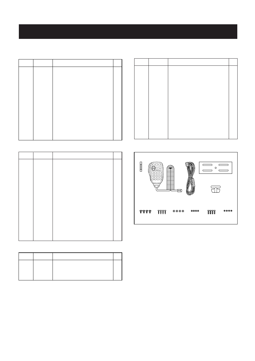
6 - 1
SECTION 6
MECHANICAL PARTS AND DISASSEMBLY
REF. NO. ORDER NO.
DESCRIPTION
QTY.
[CHASSIS PARTS]
[MAIN UNIT]
W6
8900010980 Cable OPC-1131
1
MP1
8410002380 2399 Heatsink
1
MP2
8510014470 2509 VCO case
1
MP3
8510014460 2509 VCO cover
1
REF. NO. ORDER NO.
DESCRIPTION
QTY.
Screw abbreviations
A0, B0, BT: Self-tapping
NI-ZU: Nickel-Zinc
ZK: Black
SUS: Stainless
[ACCESSORIES]
F1
5210000080 Fuse (20A)
1
MC1
0880001060 Microphone HM-133 ACC [CSA-1], [USA-2]
1
0800005740 Microphone HM-118TN ACC
[CSA]
1
0800005820 Microphone HM-118N ACC
[SEA]
1
0800005720 Microphone HM-118TAN ACC
[USA-3]
1
W1
8900010990 Cable OPC-1132 ACC
1
MP1
8010016730 150 Mobil bracket
1
MP2
8930041170
452 Felt
2
MP3
8820000530 Flange bolt M4 x 8
4
MP4
8810000950 Screw A0 M5 x 16
4
MP5
8850000180 Flat washer M5 SUS
4
MP6
8850000500 Spring washer M5 SUS
4
MP7
8810000470 Screw M5 x 12 (+/–)
4
MP8
8830000250 Nut M5 SUS
4
MP9
8930007300 MIC hanger
[USA] only
1
REF. NO. ORDER NO.
DESCRIPTION
QTY.
REF. NO. ORDER NO.
DESCRIPTION
QTY.
[LOGIC BOARD]
MC1
*
W1
MP3
MP1
MP4
MP5
MP6
MP8
MP9
F1
MP7
*
The illustration is the HM-133V.
6-1 IC-V8000
DS19
5030002250 L1-0256TAM
1
S9
2250000370 Encoder EVQ-VENF01 24B
1
SP1
2510001150
Speaker 045P0804
1
WS1
8600036880 FX2509 P01L0
1
EP9
8930057360 LCD contact SRCN-2509-SP-N-W
1
MP1
8210018440 2509 Front panel
1
MP2
8930057300 2509 LCD filter
1
MP3
8210018450 2509 Reflectort
1
MP4
8930056850 2509 A-keyboard
1
MP5
8930056860 2509 B-keyboard
1
MP6
8930056870 2509 C-keyboard
1
MP7
8510014340 2509 Front plate
1
MP8
8610010602 Knob N-267-2
2
MP9
8610011140
Knob N-291
1
MP12
8810008760 Screw B0 M2 x 8 NI-ZU (BT)
4
J1
6510004880 Connector MR-DSE-01
1
MF1
2710000720 Fan DF125020BH
1
MP1
8010018801 2509 Chassis-1 1
MP2
8030056880 2509 Fan holder
1
MP3
8110007670
2509 Cover
1
MP4
8810008660 Screw BT M3 x 8 NI-ZU (BT)
2
MP5
8810008660 Screw BT M3 x 8 NI-ZU (BT)
1
MP6
8810008660 Screw BT M3 x 8 NI-ZU (BT)
13
MP7
8810008030 Screw H M2.6 x 8
2
MP9
8810005160 Hex socket bolt M3 x 20 ZK
3
MP10
8810009610 Screw M2.6 x 6 ZK
4
MP11
8930039610 Thermally sheet (C)
3
MP14
8810010140 Screw M3 x 30 ZK
4
MP15
8510014500 2509 Shield plate
1
MP16
8930057880 Rubber sheet (BA)
1
MP17
8930048390 Sheet (BZ)
1
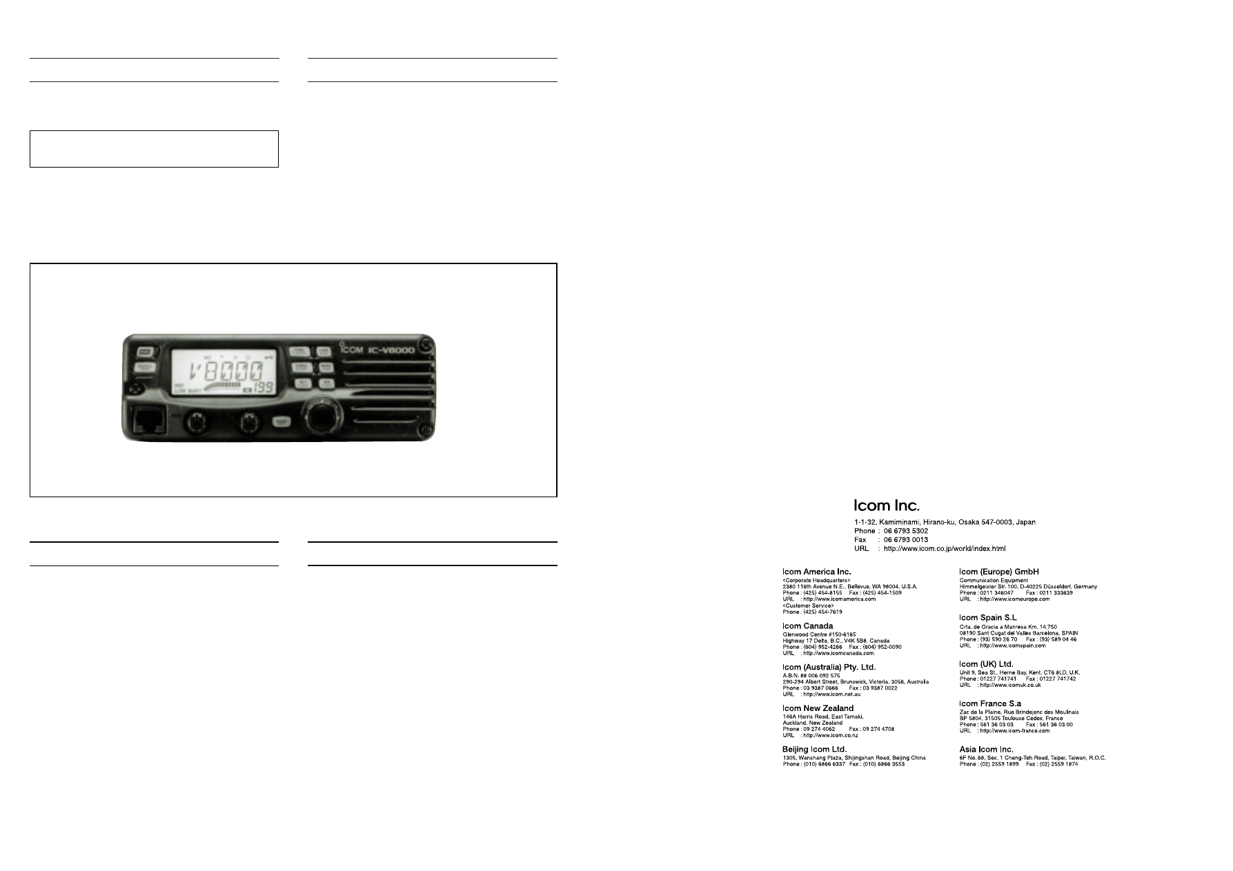
INTRODUCTION
DANGER
This service manual describes the latest service information
for the IC-V8000 VHF FM TRANSCEIVER at the time of pub-
lication.
ORDERING PARTS
Be sure to include the following four points when ordering
replacement parts:
1. 10-digit order numbers
2. Component part number and name
3. Equipment model name and unit name
4. Quantity required
<SAMPLE ORDER>
1110003200 S.IC
TA31136FN
IC-V8000 MAIN UNIT
5 pieces
8810006050 Screw Icom screw E7 IC-V8000 Chassis
10 pieces
Addresses are provided on the inside back cover for your
convenience.
NEVER connect the transceiver to an AC outlet or to a DC
power supply that uses more than 16 V. This will ruin the
transceiver.
DO NOT expose the transceiver to rain, snow or any liquids.
DO NOT reverse the polarities of the power supply when
connecting the transceiver.
DO NOT apply an RF signal of more than 20 dBm (100mW)
to the antenna connector. This could damage the trans-
ceiver's front end.
REPAIR NOTES
1. Make sure a problem is internal before disassembling
the transceiver.
2. DO NOT open the transceiver until the transceiver is dis-
connected from its power source.
3. DO NOT force any of the variable components. Turn
them slowly and smoothly.
4. DO NOT short any circuits or electronic parts. An insulat-
ed turning tool MUST be used for all adjustments.
5. DO NOT keep power ON for a long time when the trans-
ceiver is defective.
6. DO NOT transmit power into a signal generator or a
sweep generator.
7. ALWAYS connect a 50 dB to 60 dB attenuator between
the transceiver and a deviation meter or spectrum ana-
lyzer when using such test equipment.
8. READ the instructions of test equipment thoroughly
before connecting equipment to the transceiver.
To upgrade quality, any electrical or mechanical parts and
internal circuits are subject to change without notice or
obligation.

SERVICE
MANUAL
VHF FM TRANSCEIVER
1-1-32, Kamiminami, Hirano-ku, Osaka, 547-0003, Japan
S-13815IZ-C1
© 2002 Icom Inc.
Document Outline
- Front cover
- Introduction
- Table of contents
- Specifications
- Inside views
- Disassembly instructions
- Circuit description
- Parts list
- Mechanical parts and disassembly
- Address
- Back cover
Wyszukiwarka
Podobne podstrony:
hplj 5p 6p service manual vhnlwmi5rxab6ao6bivsrdhllvztpnnomgxi2ma vhnlwmi5rxab6ao6bivsrdhllvztpnnomg
Oberheim Prommer Service Manual
Korg SQ 10 Service Manual
MAC1500 service manual
Kyocera Universal Feeder UF 1 Service Manual
Proview RA783 LCD Service Manual
indesit witp82euy Service Manual
Glow Worm installation and service manual Hideaway 70CF UIS
Proview PZ456 LCD Service Manual
Glow Worm installation and service manual Ultimate 50CF UIS
ewm2000 service manual
Glow Worm installation and service manual Ultimate 60CF UIS
Proview SH770I LCD Service Manual
M23 Service Manual
Glow Worm installation and service manual Glow micron 60
Konica Minolta QMS 7115, 7118 Service Manual
Honda NSR125 '87 Service Manual
Epson Stylus Color 460 Service Manual
więcej podobnych podstron