2/28/00
.016 (0.4)
.056 (
1
.43
)
.037(0.95) .037(0.95)
ma
x
. .004
(
0.1
)
.122 (3.1)
.016 (0.4)
.016 (0.4)
1
2
3
Top View
.102 (2.6)
.007 (
0
.17
5)
.0
45 (
1
.15)
.110 (2.8)
.052 (
1
.33
)
.005
(
0
.1
25)
.094 (2.4)
.0
37 (
0
.95)
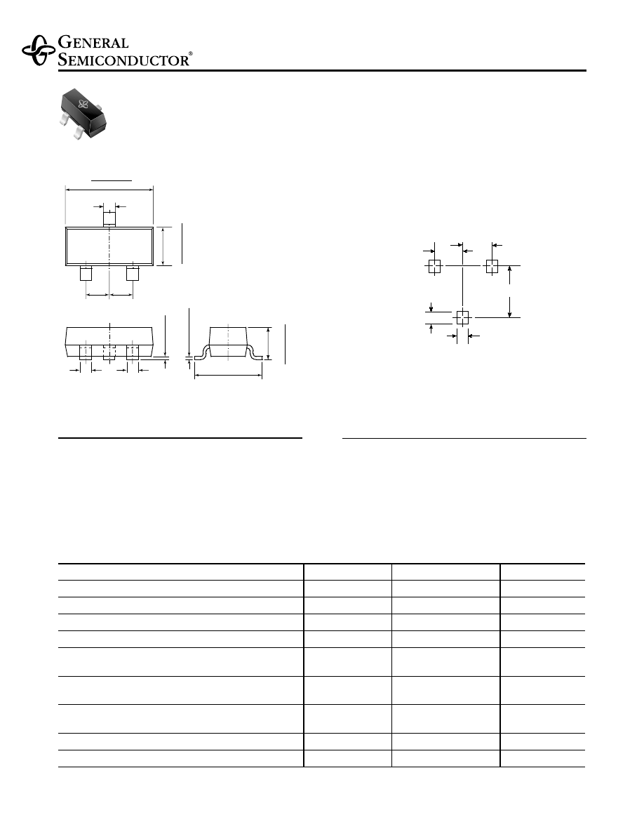
TO-236AB (SOT-23)
MMBT2222A
Small Signal Transistor (NPN)
Features
• NPN Silicon Epitaxial Planar Transistor for
switching and amplifier applications.
• This transistor is also available in the TO-92 case
with the type designation MPS2222A.
Dimensions in inches and (millimeters)
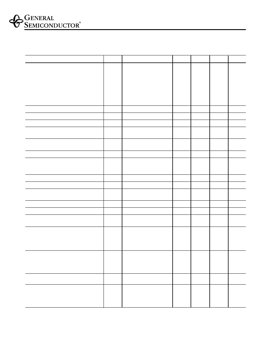
Maximum Ratings & Thermal Characteristics
Ratings at 25°C ambient temperature unless otherwise specified.
Parameters
Symbols
Value
Units
Collector-Base Voltage
V
CBO
75
V
Collector-Emitter Voltage
V
CEO
40
V
Emitter-Base Voltage
V
EBO
6.0
V
Collector Current
I
C
600
mA
Power Dissipation
on FR-5 Board
(1)
T
A
= 25°C
P
tot
225
mW
Derate above 25°C
1.8
mW/°C
Power Dissipation
on Alumina Substrate
(2)
T
A
= 25°C
P
tot
300
mW
Derate above 25°C
2.4
mW/°C
Thermal Resistance Junction
FR-5 Board
R
Θ
JA
556
°C/W
to Ambient Air
Alumina Substrate
417
Junction Temperature
T
j
150
°
C
Storage Temperature Range
T
S
– 55 to +150
°
C
Notes: (1) FR-5 = 1.0 x 0.75 x 0.062 in.
(2) Alumina = 0.4 x 0.3 x 0.024 in. 99.5% alumina.
Mechanical Data
Case: SOT-23 Plastic Package
Weight: approx. 0.008g
Marking Code: 1P
Packaging Codes/Options:
E8/10K per 13” reel (8mm tape)
E9/3K per 7” reel (8mm tape)
New Product
Pin Configuration
1 = Base 2 = Emitter
3 = Collector
0.079 (2.0)
0.037 (0.95)
0.035 (0.9)
0.031 (0.8)
0.037 (0.95)
Mounting Pad Layout
MMBT2222A
Small Signal Transistor (NPN)
Electrical Characteristics
(T
J
= 25°C unless otherwise noted)
Parameter
Symbol
Test Condition
Min
Typ
Max
Unit
V
CE =
10 V, I
C
= 0.1 mA
35
—
—
V
CE =
10 V, I
C
= 1 mA
50
—
—
V
CE =
10 V, I
C
= 10 mA
75
—
—
DC Current Gain
h
FE
V
CE =
10 V, I
C
= 10 mA
35
—
—
—
T
A
= -55°C
V
CE =
10 V, I
C
= 150 mA
(1)
100
—
300
V
CE =
10 V, I
C
= 500 mA
(1)
40
—
—
V
CE =
1.0 V, I
C
= 150 mA
(1)
50
—
—
Collector-Base Breakdown Voltage
V
(BR)CBO
I
C
= 10
µ
A, I
E
= 0
75
—
—
V
Collector-Emitter Breakdown Voltage
(1)
V
(BR)CEO
I
C
= 10 mA, I
B
= 0
40
—
—
V
Emitter-Base Breakdown Voltage
V
(BR)EBO
I
C
= 10
µ
A, I
C
= 0
6.0
—
—
V
Collector-Emitter Saturation Voltage
(1)
V
CEsat
I
C
= 150 mA, I
B
= 15 mA
—
—
0.3
V
I
C
= 500 mA, I
B
= 50 mA
—
—
1.0
Base-Emitter Saturation Voltage
(1)
V
BEsat
I
C
= 150 mA, I
B
= 15 mA
0.6
—
1.2
V
I
C
= 500 mA, I
B
= 50 mA
—
—
2.0
Collector Cut-off Current
I
CEX
V
EB
= 3 V, V
CE
= 60 V
—
—
10
nA
V
CB
= 60 V, I
E
= 0
—
—
10
nA
Collector Cut-off Current
I
CBO
V
CB
= 50 V, I
E
= 0 V
—
—
10
µ
A
T
A
= 125°C
Base Cut-off Current
I
BL
V
EB
= 3 V, V
CE
= 60 V
—
—
20
nA
Emitter Cut-off Current
I
EBO
V
EB
= 3 V
DC
, I
C
= 0
—
—
100
nA
Current Gain-Bandwidth Product
f
T
V
CE
= 20 V, I
C
= 20 mA
300
—
—
MHz
f = 100 MHz
Output Capacitance
C
obo
V
CB
= 10 V, f = 1 MHz, I
E
= 0
—
—
8
pF
Input Capacitance
C
ibo
V
EB
= 0.5 V, f = 1 MHz, I
C
= 0
—
—
25
pF
Noise Figure
NF
V
CE
= 10 V, I
C
= 100
µ
A,
—
—
4.0
dB
R
S
= 1 k
Ω
, f = 1 kHz
V
CE
= 10 V, I
C
= 1 mA
2
—
8.0
Input Impedance
h
ie
f = 1 kHz
k
Ω
V
CE
= 10 V, I
C
= 10 mA
0.25
—
1.25
f = 1 kHz
V
CE
= 10 V, I
C
= 1 mA,
50
—
300
Small Signal Current Gain
h
fe
f = 1 kHz
—
V
CE
= 10 V, I
C
= 10 mA,
75
—
375
f = 1 kHz
Voltage Feedback Ratio
h
re
V
CE
= 10 V, I
C
= 1 mA,
50
—
300
—
f = 1 kHz
75
—
375
V
CE
= 10 V, I
C
= 1 mA,
5.0
—
35
Output Admittance
h
oe
f = 1 kHz
µ
S
V
CE
= 10 V, I
C
= 10 mA,
25
—
200
f = 1 kHz
Note:
(1) Pulse Test: Pulse width
≤
300
µ
s - Duty cycle
≤
2%
MMBT2222A
Small Signal Transistors (NPN)
Electrical Characteristics
(T
J
= 25°C unless otherwise noted)
Parameter
Symbol
Test Condition
Min
Typ
Max
Unit
Collector Base Time Constant
r
b
’C
C
I
E
= 20 mA, V
CB
= 20 V,
—
—
150
ps
f = 31.8 MHz
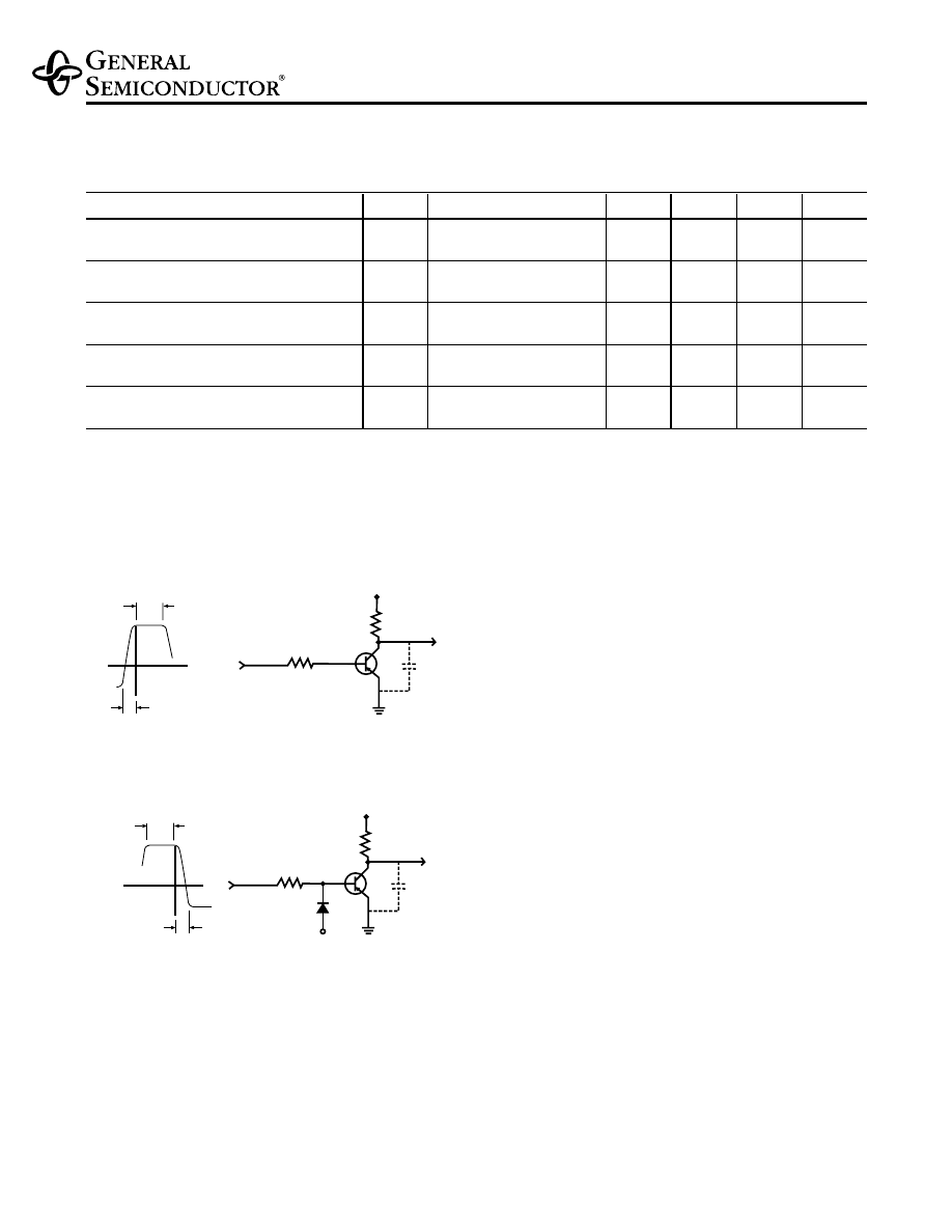
Delay Time (see fig. 1)
t
d
I
B1
= 15 mA, I
C
= 150 mA,
—
—
10
ns
V
CC =
30V, V
BE
= -0.5 V
Rise Time (see fig. 1)
t
r
I
B1
= 15 mA, I
C
= 150 mA,
—
—
25
ns
V
CC =
30V, V
BE
= -0.5 V
Storage Time (see fig. 2)
t
s
I
B1
= I
B2
= 15 mA,
—
—
225
ns
I
C
= 150 mA, V
CC =
30V
Fall Time (see fig. 2)
t
f
I
B1
= I
B2
= 15 mA,
—
—
60
ns
I
C
= 150 mA, V
CC =
30V
< 2 ns
0
C * < 10 pF
S
200
Ω
1.0 to 100
µ
s, DUTY CYCLE
≈
2%
+30V
+16 V
-2 V
1k
Ω
Scope rise time < 4ns
*Total shunt capacitance of test jig,
connectors and oscilloscope
Switching Time Equivalent Test Circuit
Figure 1. Turn-ON Time
Figure 2. Turn-OFF Time
200
Ω
+30V
-4 V
C < 10 pF
S
*
1.0 to 100
µ
s, DUTY CYCLE
≈
2%
1k
Ω
< 20 ns
0
+16 V
-14 V
Wyszukiwarka
Podobne podstrony:
MMBT2222
PN2222A, MMBT2222A, PZT2222A (Fairchild Semiconductor)
MMBT2222A, SMBT2222A (Infineon)
więcej podobnych podstron