SMBT2222A/ MMBT2222A
1
Feb-18-2002
NPN Silicon Switching Transistor
High DC current gain: 0.1mA to 500 mA
Low collector-emitter saturation voltage
Complementary type: SMBT2907A (PNP)
1
2
3
VPS05161
Type
Marking
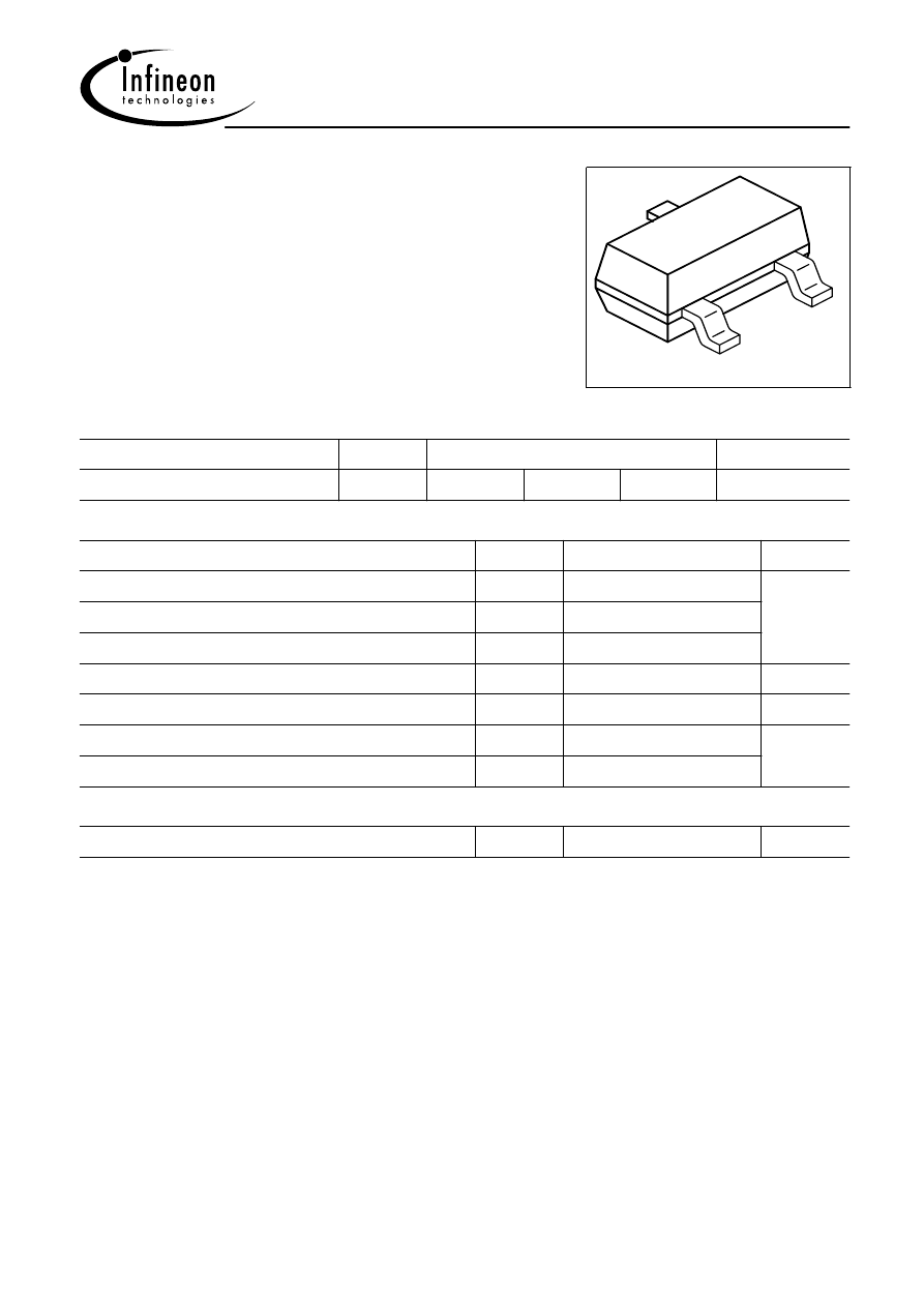
Pin Configuration
Package
SMBT2222A/ MMBT2222A
s1P
1=B
2=E
3=C
SOT23
Maximum Ratings
Parameter
Symbol
Value
Unit
Collector-emitter voltage
V
CEO
40
V
Collector-base voltage
V
CBO
75
Emitter-base voltage
V
EBO
6
DC collector current
I
C
600
mA
Total power dissipation
,
T
S
= 77 °C
P
tot
330
mW
Junction temperature
T
j
150
°C
Storage temperature
T
stg
-65 ... 150
Thermal Resistance
Junction - soldering point
1)
R
thJS
220
K/W
1For calculation of R
thJA
please refer to Application Note Thermal Resistance

SMBT2222A/ MMBT2222A
2
Feb-18-2002
Electrical Characteristics at T
A
= 25°C, unless otherwise specified
Parameter
Symbol
Values
Unit
min.
typ.
max.
DC Characteristics
Collector-emitter breakdown voltage
I
C
= 10 mA,
I
B
= 0
V
(BR)CEO
40
-
-
V
Collector-base breakdown voltage
I
C
= 10 µA,
I
E
= 0
V
(BR)CBO
75
-
-
Emitter-base breakdown voltage
I
E
= 10 µA,
I
C
= 0
V
(BR)EBO
6
-
-
Collector cutoff current
V
CB
= 60 V,
I
E
= 0
I
CBO
-
-
10
nA
Collector cutoff current
V
CB
= 60 V,
I
E
= 0 ,
T
A
= 150 °C
I
CBO
-
-
10
µA
Emitter cutoff current
V
EB
= 3 V,
I
C
= 0
I
EBO
-
-
10
nA
DC current gain 1)
I
C
= 100 µA,
V
CE
= 10 V
I
C
= 1 mA,
V
CE
= 10 V
I
C
= 10 mA,
V
CE
= 10 V
I
C
= 150 mA,
V
CE
= 1 V
I
C
= 150 mA,
V
CE
= 10 V
I
C
= 500 mA,
V
CE
= 10 V
I
C
= 10 mA, V
CE
= 10 V, T
A
= 55°C
h
FE
35
50
75
50
100
40
35
-
-
-
-
-
-
-
-
-
-
-
300
-
-
-
Collector-emitter saturation voltage1)
I
C
= 150 mA,
I
B
= 15 mA
I
C
= 500 mA,
I
B
= 50 mA
V
CEsat
-
-
-
-
0.3
1
V
Base-emitter saturation voltage 1)
I
C
= 150 mA,
I
B
= 15 mA
I
C
= 500 mA,
I
B
= 50 mA
V
BEsat
0.6
-
-
-
1.2
2
1) Pulse test: t
≤
=
300
µ
s, D = 2%

SMBT2222A/ MMBT2222A
3
Feb-18-2002
Electrical Characteristics at T
A
= 25°C, unless otherwise specified
Parameter
Symbol
Values
Unit
min.
typ.
max.
AC Characteristics
Transition frequency
I
C
= 20 mA,
V
CE
= 20 V,
f
= 100 MHz
f
T
300
-
-
MHz
Collector-base capacitance
V
CB
= 10 V,
f
= 1 MHz
C
cb
-
-
8
pF
Emitter-base capacitance
V
EB
= 0.5 V,
f
= 1 MHz
C
eb
-
-
25
Noise figure
I
C
= 100 µA,
V
CE
= 10 V,
R
S
= 1
k
,
f
= 1 kHz,
f
= 200
Hz
F
-
-
4
dB
Short-circuit input impedance
I
C
= 1 mA,
V
CE
= 10 V,
f
= 1 kHz
I
C
= 10 mA,
V
CE
= 10 V,
f
= 1 kHz
h
11e
2
0.25
-
-
8
1.25
k
Open-circuit reverse voltage transf.ratio
I
C
= 1 mA,
V
CE
= 10 V,
f
= 1 kHz
I
C
= 10 mA,
V
CE
= 10 V,
f
= 1 kHz
h
12e
-
-
-
-
8
4
10
-4
Short-circuit forward current transf.ratio
I
C
= 1 mA,
V
CE
= 10 V,
f
= 1 kHz
I
C
= 10 mA,
V
CE
= 10 V,
f
= 1 kHz
h
21e
50
75
-
-
300
375
-
Open-circuit output admittance
I
C
= 1 mA,
V
CE
= 10 V,
f
= 1 kHz
I
C
= 10 mA,
V
CE
= 10 V,
f
= 1 kHz
h
22e
5
25
-
-
35
200
S
Delay time
V
CC
= 30 V,
I
C
= 150 mA,
I
B1
= 15 mA,
V
BE(off)
= 0.5 V
t
d
-
-
10
ns
Rise time
V
CC
= 30 V,
I
C
= 150 mA,
I
B1
= 15 mA,
V
BE(off)
= 0.5 V
t
r
-
-
25
Storage time
V
CC
= 30 V,
I
C
= 150 mA, I
B1
=I
B2
= 15mA
t
stg
-
-
225
ns
Fall time
V
CC
= 30 V,
I
C
= 150 mA, I
B1
=
IB2 = 15mA
t
f
-
-
60
ns
SMBT2222A/ MMBT2222A
4
Feb-18-2002
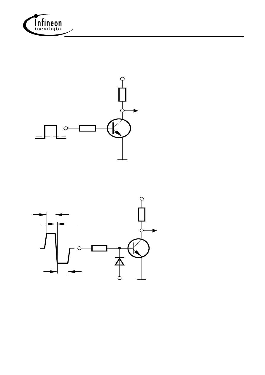
Test circuits
Delay and rise time
EHN00055
200
Osc.
619
30
9.9
0
0.5
Ω
Ω
V
V
V
Storage and fall time
EHN00056
200
Osc.
1
30
16.2
0
-13.8
-3.0
µ
500
~
s
s
~100
µ
< 5 ns
Ω
Ω
V
V
V
V
k
Oscillograph
: R > 100
Ω
, C < 12pF, t
r
< 5ns
SMBT2222A/ MMBT2222A
5
Feb-18-2002
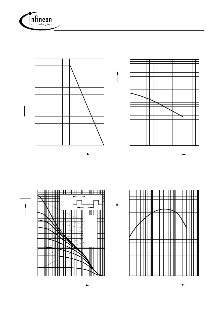
Collector-base capacitance
C
CB
= f (V
CB
)
f
= 1MHz
EHP00739
SMBT 2222/A
10
pF
10
10
V
C
CB
10
5
10
cb
5
5
-1
0
1
2
10
2
1
10
0
5
V
Total power dissipation
P
tot
= f(T
S
)
0
15
30
45
60
75
90 105 120
°C
150
T
S
0
30
60
90
120
150
180
210
240
270
300
mW
360
P
tot
Permissible pulse load
P
totmax
/ P
totDC
= f (t
p
)
10
EHP00740
SMBT 2222/A
-6
0
10
5
D =
5
10
1
5
10
2
3
10
10
-5
10
-4
10
-3
10
-2
10
0
s
0
0.005
0.01
0.02
0.05
0.1
0.2
0.5
t
p
=
D
T
t
p
T
tot max
tot
P
DC
P
p
t
Transition frequency
f
T
= f (I
C
)
V
CE
= 20V
EHP00741
SMBT 2222/A
10
10
10
mA
f
C
10
MHz
10
T
5
5
5
Ι
0
1
2
3
10
3
2
10
1
5
2
2
SMBT2222A/ MMBT2222A
6
Feb-18-2002
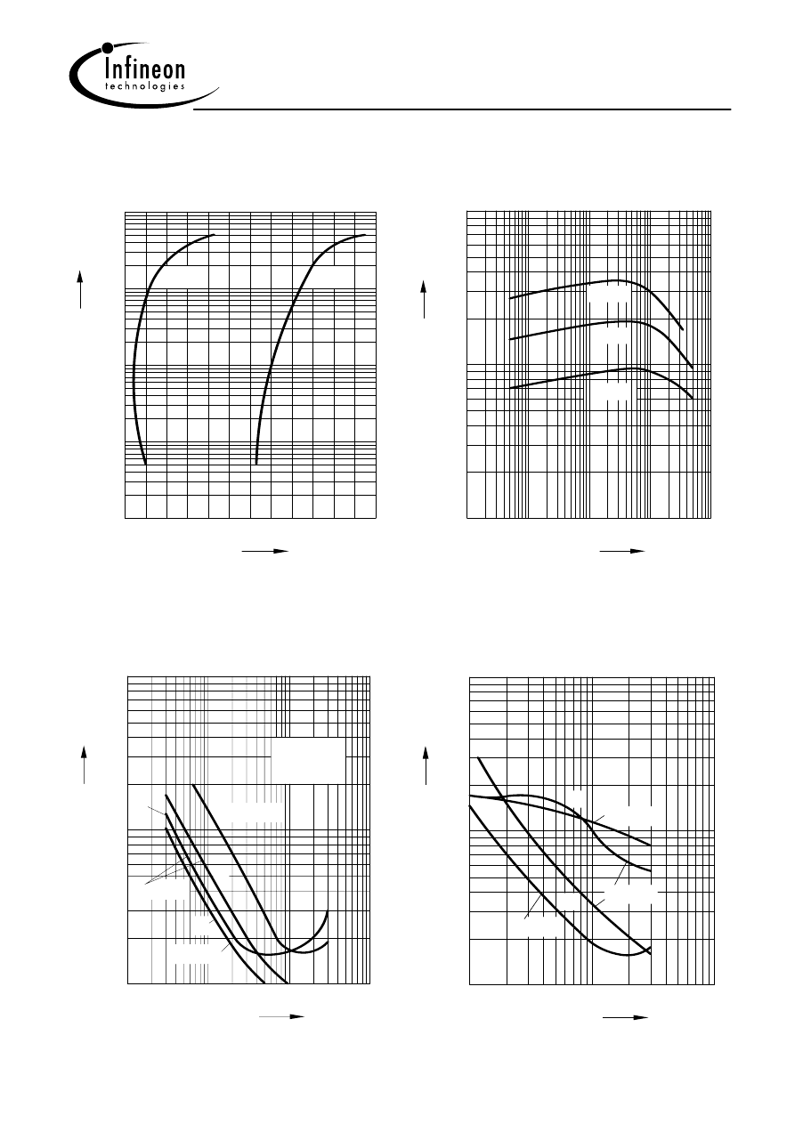
Saturation voltage
I
C
= f (V
BEsat
, V
CEsat
)
h
FE
= 10
EHP00742
SMBT 2222/A
10
0
V
BE sat
mA
10
3
1
10
-1
5
10
0
5
V
0.2
0.4
0.6
0.8
1.0
1.2
CE sat
V
,
5
10
2
V
BE
V
CE
Ι
C
DC current gain
h
FE
= f (I
C
)
V
CE
= 10V
EHP00743
SMBT 2222/A
10
10
mA
h
C
10
5
FE
10
3
2
10
1
5
10
10
10
-1
0
1
2
3
Ι
-50 ˚C
25 ˚C
150 ˚C
Delay time
t
d
= f (I
C
)
Rise time
t
r
= f (I
C
)
EHP00744
SMBT 2222/A
10
ns
10
10
mA
t
C
10
5
10
d
5
5
5
Ι
0
1
2
3
10
3
2
10
1
5
r
t
,
h
FE
t
d
t
d
t
r
t
r
V
CC
= 30 V
= 10
V
BE
= 5 V
= 2 V
= 0 V
V
BE
V
BE
Storage time
t
stg
= f (I
C
)
Fall time
t
f
= f (I
C
)
EHP00745
SMBT 2222/A
10
10
mA
C
5
10
3
2
10
1
5
10
10
1
2
3
Ι
5
5
ns
FE
h
h
FE
s
t
f
t
= 10
= 20
s
t t
,
f
h
FE
= 10
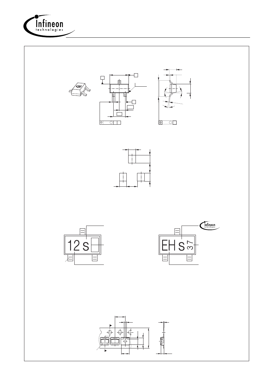
Package SOT23
P a c k a g e O u t l i n e
F o o t P r i n t
M a r k i n g L a y o u t
P a c k i n g
Code E6327: Reel ø180 mm = 3.000 Pieces/Reel
Code E6433: Reel ø330 mm = 10.000 Pieces/Reel
2.6 MAX.
0.25
M
B C
1.9
-0.05
+0.1
0.4
1
A
2
±0.1
3
2.9
DIN 6784
+0.2
acc. to
0.95
C
B
2˚ 30˚
0.20
...
M
A
0.1 MAX.
10
˚
0.08...0.15
1.1 MAX.
1.3
±0.1
MAX.
10
˚
MAX.
0.8
1.2
0.9
1.1
0.9
0.8
Manufacturer
Date code (Year/Month)
Type code
2003, July
BCW66
Example
Pin 1
3.15
4
2.65
2.13
0.9
8
0.2
1.15
Pin 1

Impressum
Published by Infineon Technologies AG,
St.-Martin-Strasse 53,
81669 München
© Infineon Technologies AG 2005.
All Rights Reserved.
Attention please!
The information herein is given to describe certain components and shall not be
considered as a guarantee of characteristics.
Terms of delivery and rights to technical change reserved.
We hereby disclaim any and all warranties, including but not limited to warranties of
non-infringement, regarding circuits, descriptions and charts stated herein.
Information
For further information on technology, delivery terms and conditions and prices
please contact your nearest Infineon Technologies Office (www.Infineon.com).
Warnings
Due to technical requirements components may contain dangerous substances.
For information on the types in question please contact your nearest Infineon
Technologies Office.
Infineon Technologies Components may only be used in life-support devices or
systems with the express written approval of Infineon Technologies, if a failure of
such components can reasonably be expected to cause the failure of that life-support
device or system, or to affect the safety or effectiveness of that device or system.
Life support devices or systems are intended to be implanted in the human body, or
to support and/or maintain and sustain and/or protect human life. If they fail, it is
reasonable to assume that the health of the user or other persons may be endangered.
Wyszukiwarka
Podobne podstrony:
MMBT2222
PN2222A, MMBT2222A, PZT2222A (Fairchild Semiconductor)
MMBT2222
MMBT2907A, SMBT2907A (Infineon)
MMBT3904, SMBT3904 (Infineon)
TCA105 Infineon elenota pl
Infineon Plans
BC807, BC808 (Infineon)
BSS92 (Infineon)
MMBT3906, SMBT3906 (Infineon)
BC857S (Infineon)
BSS88 (Infineon)
więcej podobnych podstron