TL/F/6526
5474/DM5474/DM7474
Dual
Positive-Edge-Triggered
D
Flip-Flops
with
Preset,
Clear
and
Complementary
Outputs
June 1989
5474/DM5474/DM7474
Dual Positive-Edge-Triggered D Flip-Flops
with Preset, Clear and Complementary Outputs
General Description
This device contains two independent positive-edge-trig-
gered D flip-flops with complementary outputs. The informa-
tion on the D input is accepted by the flip-flops on the posi-
tive going edge of the clock pulse. The triggering occurs at a
voltage level and is not directly related to the transition time
of the rising edge of the clock. The data on the D input may
be changed while the clock is low or high without affecting
the outputs as long as the data setup and hold times are not
violated. A low logic level on the preset or clear inputs will
set or reset the outputs regardless of the logic levels of the
other inputs.
Features
Y
Alternate Military/Aerospace device (5474) is available.
Contact a National Semiconductor Sales Office/Distrib-
utor for specifications.
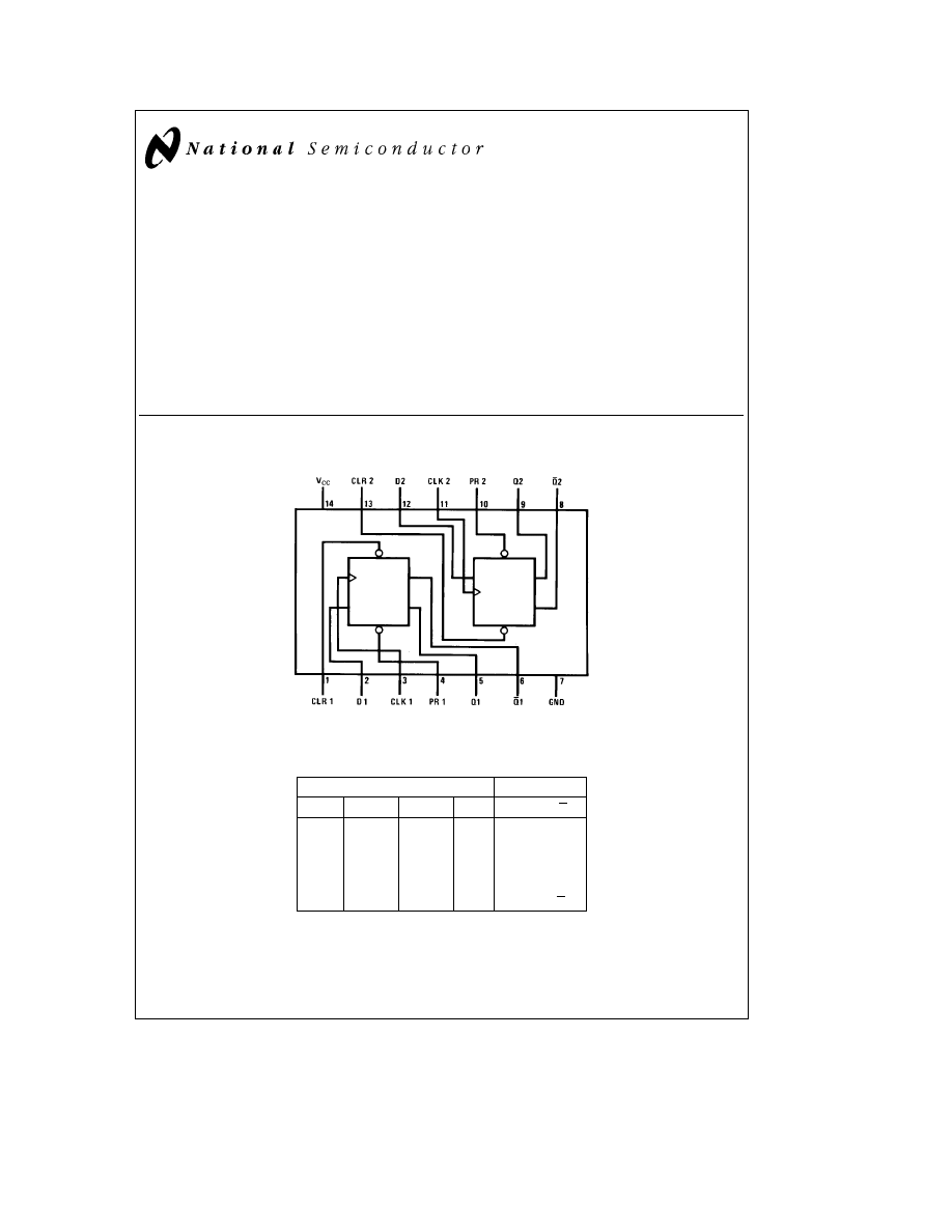
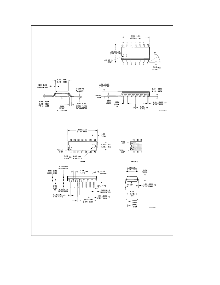
Connection Diagram
Dual-In-Line Package
TL/F/6526 – 1
Order Number 5474DMQB, 5474FMQB, DM5474J, DM5474W, DM7474M or DM7474N
See NS Package Number J14A, M14A, N14A or W14B
Function Table
Inputs
Outputs
PR
CLR
CLK
D
Q
Q
L
H
X
X
H
L
H
L
X
X
L
H
L
L
X
X
H*
H*
H
H
u
H
H
L
H
H
u
L
L
H
H
H
L
X
Q
0
Q
0
H
e
High Logic Level
X
e
Either Low or High Logic Level
L
e
Low Logic Level
u
e
Positive-going transition of the clock.
*
e
This configuration is nonstable; that is, it will not persist when either the preset and/or clear
inputs return to their inactive (high) level.
Q
0
e
The output logic level of Q before the indicated input conditions were established.
C1995 National Semiconductor Corporation
RRD-B30M105/Printed in U. S. A.
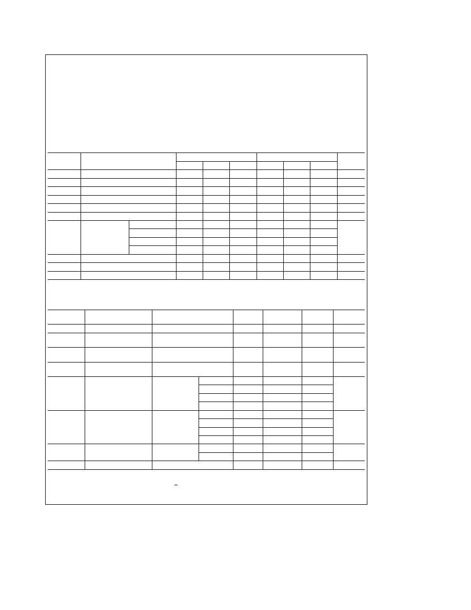
Absolute Maximum Ratings
(Note)
If Military/Aerospace specified devices are required,
please contact the National Semiconductor Sales
Office/Distributors for availability and specifications.
Supply Voltage
7V
Input Voltage
5.5V
Operating Free Air Temperature Range
DM54 and 54
b
55
§
C to
a
125
§
C
DM74
0
§
C to
a
70
§
C
Storage Temperature Range
b
65
§
C to
a
150
§
C
Note:
The ‘‘Absolute Maximum Ratings’’ are those values
beyond which the safety of the device cannot be guaran-
teed. The device should not be operated at these limits. The
parametric values defined in the ‘‘Electrical Characteristics’’
table are not guaranteed at the absolute maximum ratings.
The ‘‘Recommended Operating Conditions’’ table will define
the conditions for actual device operation.
Recommended Operating Conditions
Symbol
Parameter
DM5474
DM7474
Units
Min
Nom
Max
Min
Nom
Max
V
CC
Supply Voltage
4.5
5
5.5
4.75
5
5.25
V
V
IH
High Level Input Voltage
2
2
V
V
IL
Low Level Input Voltage
0.8
0.8
V
I
OH
High Level Output Current
b
0.4
b
0.4
mA
I
OL
Low Level Output Current
16
16
mA
f
CLK
Clock Frequency (Note 2)
0
15
0
15
MHz
t
W
Pulse Width
Clock High
30
30
(Note 2)
Clock Low
37
37
ns
Clear Low
30
30
Preset Low
30
30
t
SU
Input Setup Time (Notes 1 & 2)
20
u
20
u
ns
t
H
Input Hold Time (Notes 1 & 2)
5
u
5
u
ns
T
A
Free Air Operating Temperature
b
55
125
0
70
§
C
Note 1:
The symbol (
u
) indicates the rising edge of the clock pulse is used for reference.
Note 2:
T
A
e
25
§
C and V
CC
e
5V.
Electrical Characteristics
over recommended operating free air temperature range (unless otherwise noted)
Symbol
Parameter
Conditions
Min
Typ
Max
Units
(Note 3)
V
I
Input Clamp Voltage
V
CC
e
Min, I
I
e b
12 mA
b
1.5
V
V
OH
High Level Output
V
CC
e
Min, I
OH
e
Max
2.4
3.4
V
Voltage
V
IL
e
Max, V
IH
e
Min
V
OL
Low Level Output
V
CC
e
Min, I
OL
e
Max
0.2
0.4
V
Voltage
V
IH
e
Min, V
IL
e
Max
I
I
Input Current
@
Max
V
CC
e
Max, V
I
e
5.5V
1
mA
Input Voltage
I
IH
High Level Input
V
CC
e
Max
D
40
Current
V
I
e
2.4V
Clock
80
m
A
Clear
120
Preset
40
I
IL
Low Level Input
V
CC
e
Max
D
b
1.6
Current
V
I
e
0.4V
Clock
b
3.2
mA
(Note 6)
Clear
b
3.2
Preset
b
1.6
I
OS
Short Circuit
V
CC
e
Max
DM54
b
20
b
55
mA
Output Current
(Note 4)
DM74
b
18
b
55
I
CC
Supply Current
V
CC
e
Max (Note 5)
17
30
mA
Note 3:
All typicals are at V
CC
e
5V, T
A
e
25
§
C.
Note 4:
Not more than one output should be shorted at a time.
Note 5:
With all outputs open, I
CC
is measured with the Q and Q outputs high in turn. At the time of measurement the clock is grounded.
Note 6:
Clear is tested with preset high and preset is tested with clear high.
2
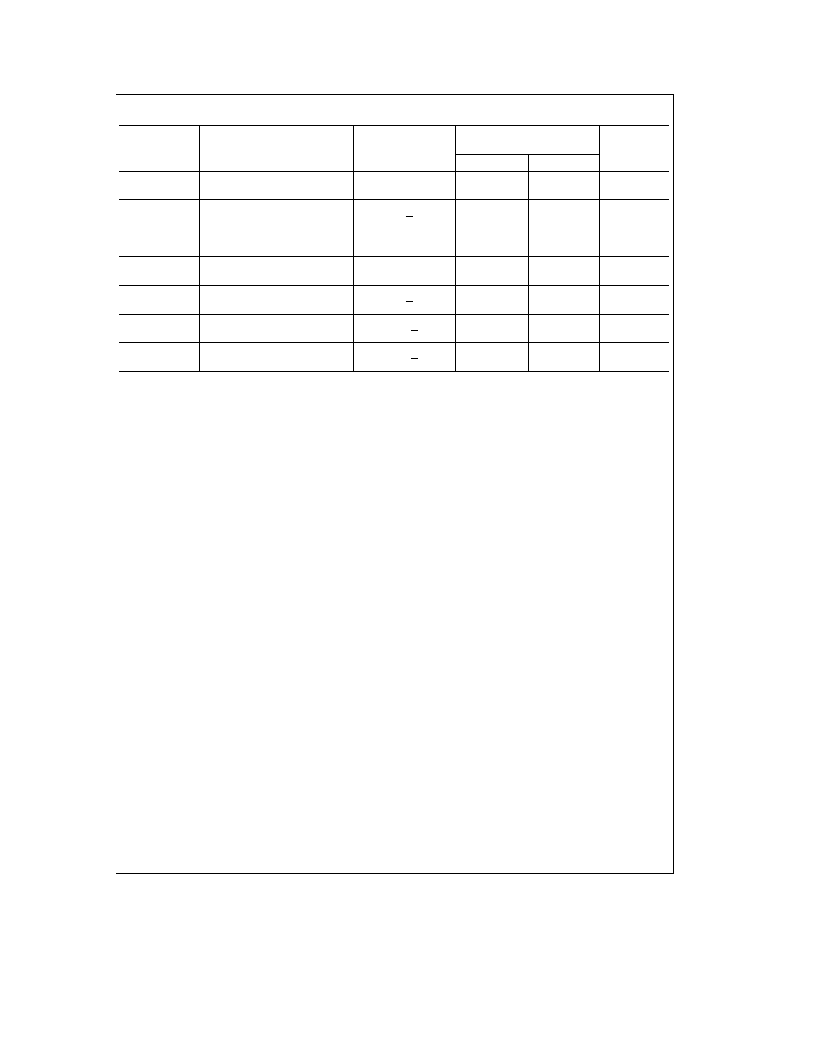
Switching Characteristics
at V
CC
e
5V and T
A
e
25
§
C (See Section 1 for Test Waveforms and Output Load)
From (Input)
R
L
e
400X
Symbol
Parameter
To (Output)
C
L
e
15 pF
Units
Min
Max
f
MAX
Maximum Clock
15
MHz
Frequency
t
PHL
Propagation Delay Time
Preset
40
ns
High to Low Level Output
to Q
t
PLH
Propagation Delay Time
Preset
25
ns
Low to High Level Output
to Q
t
PHL
Propagation Delay Time
Clear
40
ns
High to Low Level Output
to Q
t
PLH
Propagation Delay Time
Clear
25
ns
Low to High Level Output
to Q
t
PHL
Propagation Delay Time
Clock to
40
ns
High to Low Level Output
Q or Q
t
PLH
Propagation Delay Time
Clock to
25
ns
Low to High Level Output
Q or Q
3
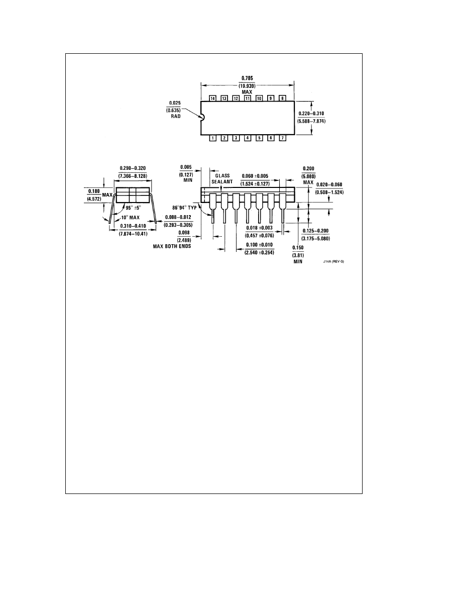
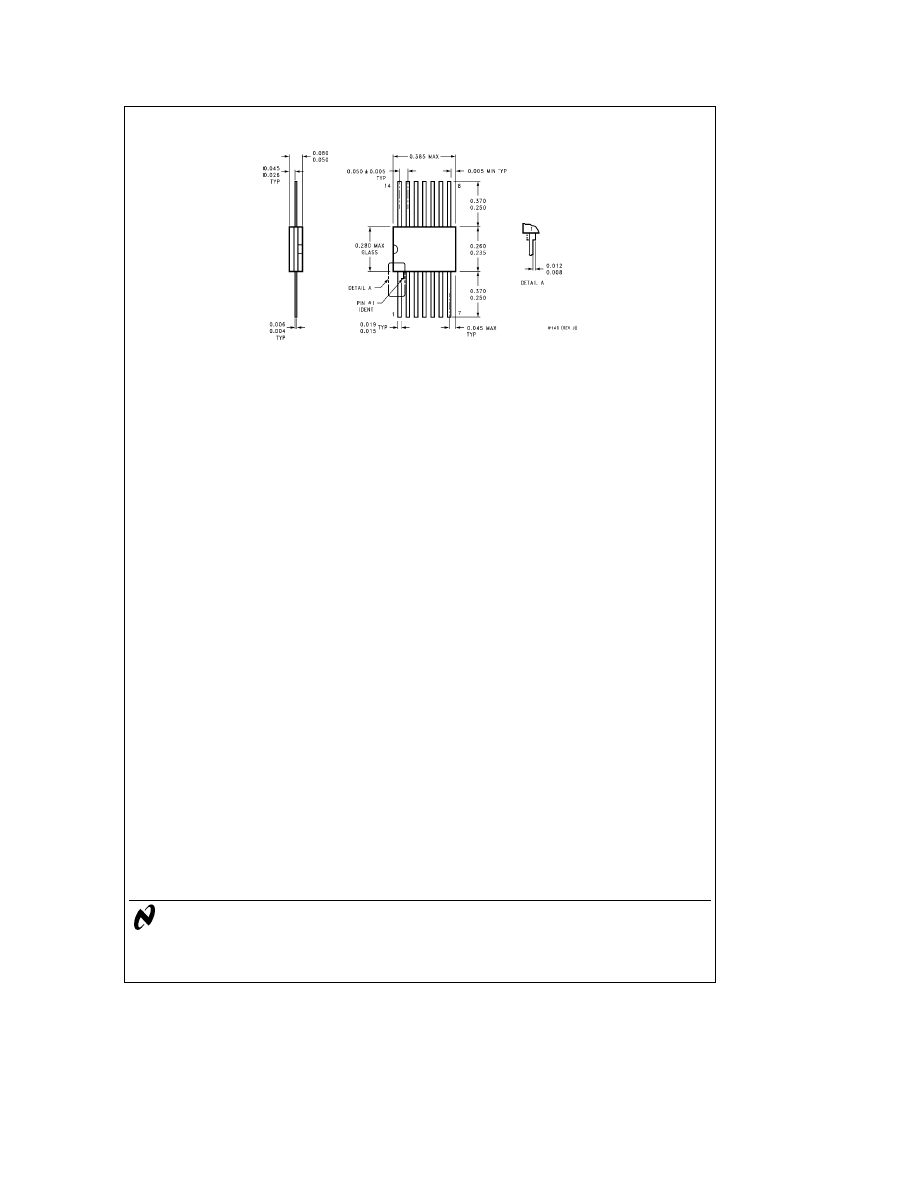
Physical Dimensions
inches (millimeters)
14-Lead Ceramic Dual-In-Line Package (J)
Order Number 5474DMQB or DM5474J
NS Package Number J14A
4
Physical Dimensions
inches (millimeters) (Continued)
14-Lead Small Outline Molded Package (M)
Order Number DM7474M
NS Package Number M14A
14-Lead Molded Dual-In-Line Package (N)
Order Number DM7474N
NS Package Number N14A
5
5474/DM5474/DM7474
Dual
Positive-Edge-Triggered
D
Flip-Flops
with
Preset,
Clear
and
Complementary
Outputs
Physical Dimensions
inches (millimeters) (Continued)
14-Lead Ceramic Flat Package (W)
Order Number 5474FMQB or DM5474W
NS Package Number W14B
LIFE SUPPORT POLICY
NATIONAL’S PRODUCTS ARE NOT AUTHORIZED FOR USE AS CRITICAL COMPONENTS IN LIFE SUPPORT
DEVICES OR SYSTEMS WITHOUT THE EXPRESS WRITTEN APPROVAL OF THE PRESIDENT OF NATIONAL
SEMICONDUCTOR CORPORATION. As used herein:
1. Life support devices or systems are devices or
2. A critical component is any component of a life
systems which, (a) are intended for surgical implant
support device or system whose failure to perform can
into the body, or (b) support or sustain life, and whose
be reasonably expected to cause the failure of the life
failure to perform, when properly used in accordance
support device or system, or to affect its safety or
with instructions for use provided in the labeling, can
effectiveness.
be reasonably expected to result in a significant injury
to the user.
National Semiconductor
National Semiconductor
National Semiconductor
National Semiconductor
Corporation
Europe
Hong Kong Ltd.
Japan Ltd.
1111 West Bardin Road
Fax: (a49) 0-180-530 85 86
13th Floor, Straight Block,
Tel: 81-043-299-2309
Arlington, TX 76017
Email: cnjwge
@
tevm2.nsc.com
Ocean Centre, 5 Canton Rd.
Fax: 81-043-299-2408
Tel: 1(800) 272-9959
Deutsch Tel: (a49) 0-180-530 85 85
Tsimshatsui, Kowloon
Fax: 1(800) 737-7018
English
Tel: (a49) 0-180-532 78 32
Hong Kong
Fran
3ais Tel: (a49) 0-180-532 93 58
Tel: (852) 2737-1600
Italiano
Tel: (a49) 0-180-534 16 80
Fax: (852) 2736-9960
National does not assume any responsibility for use of any circuitry described, no circuit patent licenses are implied and National reserves the right at any time without notice to change said circuitry and specifications.

This datasheet has been download from:
Datasheets for electronics components.
Wyszukiwarka
Podobne podstrony:
praca-magisterska-wa-c-7474, Dokumenty(2)
7474
08 Patomorfologiaid 7474 ppt
7474
7474
7474
7474
7474
7474
7474
7474
praca-magisterska-wa-c-7474, Dokumenty(2)
praca magisterska 7474
7474
islcollective worksheets grundstufe a1 grundschule klassen 14 haupt und realschule klassen 513 erwac
więcej podobnych podstron