Making Electronic Design Easy
™
Protel
99

8
6
Bring a new approach to graphical
printed circuit board design with
Protel 99’s superb PCB editor. The
PCB editor combines manual and
automated design in an interactive
environment that supports both
the new user and the experienced
designer. The underlying PCB data
structure is tuned for speed, and a
set of powerful design rules gives
you total control over the design
parameters. Equipped with manual
and interactive features that make
it easy to layout and route the most
complex mixed-technology designs,
Protel 99’s PCB editor is the perfect
balance of power and control.
Comprehensive design
rules ensure your design
meets the specs
PCB design can be a minefield
of conflicting requirements.
High-speed logic and smaller, more
complex packaging technologies
place extreme demands on the PCB
designer. Net impedance, track
clearances, signal reflections, path
lengths, critical trace widths - all
these factors and many more need
to be carefully monitored and
controlled to produce a successful
board design. Protel 99’s powerful
rules-driven design approach leaves
you free to focus on laying out and
routing the board while your
critical design requirements are
automatically monitored and
managed by the system.
Protel 99’s PCB Editor incorporates
over 25 design rule classes covering
areas such as component placement,
critical-net trace widths, crosstalk
constraints, net impedance, signal
reflections, clearances, object geom-
etry, parallelism, routing priority and
routing topology. Combined with the
ability to create multiple rules, each
applying to particular objects, nets,
components, regions, or the whole
board, Protel 99 gives you total
control over the design process.
The ability to create compound rule
scopes allows you to precisely target
the objects a rule applies to. With
simple-to-construct compound scope
definitions you can route a net at
one width on the top layer, and a
different width on the bottom layer.
Or close the solder mask over the
vias on the bottom layer, but not
the top layer.
One-click PCB-to-schematic
design synchronization
Design is not a simple linear
process. Changes and updates are
often made throughout the design
cycle and it’s all too easy for the
final board layout to get out of step
with the original schematics. With
Protel 99’s easy-to-use Design
Synchronizer, keeping your
schematic and PCB documents
in complete harmony is a breeze.
Reflecting PCB changes back to
the schematic is as easy as pressing
a button.
The Design Synchronizer analyzes
the source PCB document and target
schematic design to determine any
differences. If you have changed
component designators on your PCB
for example, the designators on the
schematic are automatically updated.
The Design Synchronizer can be
run at any stage in the board layout
process to ensure the total integrity
of your design documentation. With
Protel 99’s Design Synchronizer
technology you'll have complete
confidence that your schematic and
PCB documents represent the same
circuit throughout the design
process.
Intuitive editing environ-
ment = ease of design
Protel 99’s PCB editor is based on
familiar Windows-based graphical
editing techniques to make PCB
design a natural and intuitive
Powerful rules-driven design accelerates
Visit www.protel.com For more product information.
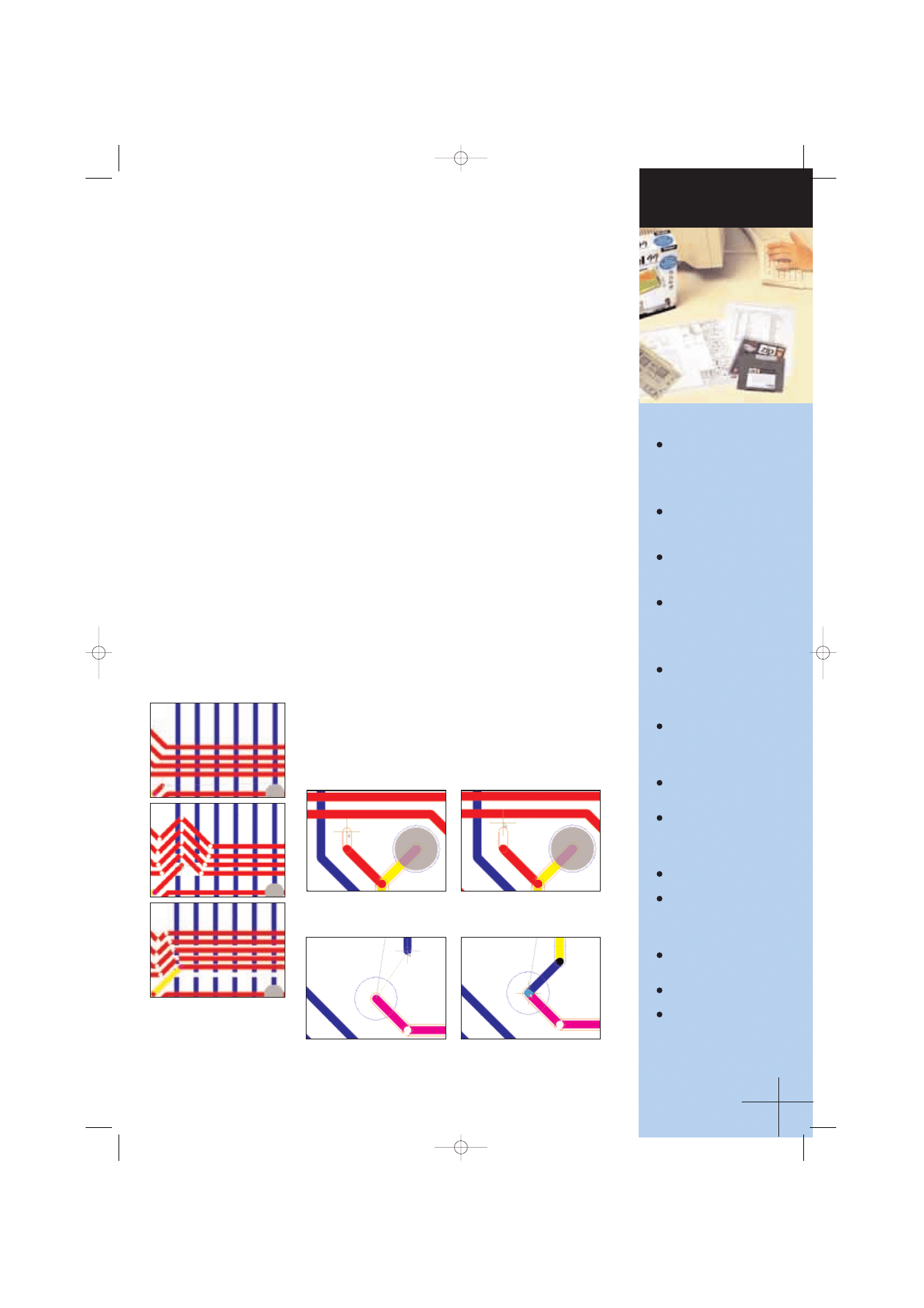
Protel 99’s PCB Editor incorporates over 25 design rule classes covering areas such as routing, manufacturing,
high-speed design, component placement, and signal integrity. Combined with the ability to create multiple rules,
each with a different scope, Protel 99 gives you total control over the design process. The ability to create
compound rule scopes allows you to precisely target the objects a rule applies to.
q3 catalog web english v2.qxd 9/7/99 10:55 AM Page 8
9
7
place components grouped first by
connectivity (creating clusters of
components), then by the component
geometry.
With higher component counts,
Protel 99’s Statistical Placer uses
an AI-based methodology called
“simulated annealing”. It analyzes
the entire design during placement,
considering the connection length,
the connection density on the
board, and the alignment of the
components, all in accordance
with the specified design rules.
Smart interactive placement tools
make short work of manual
placement jobs. Use the Auto Select
placement mode to quickly ‘collect’
components with similar footprints,
then rotate, expand and contract the
entire group as you move them to
the required location on the board.
Once your rough placement is
complete, use Auto Align mode to
neatly expand or contract a group
of placed components with similar
footprints. These and many other
advanced interactive features make
component placement in Protel 99
a designer’s dream.
Effortless interactive
manual routing
A major challenge for today’s PCB
designer is working with a mix of
imperial and metric technologies.
Protel 99’s powerful manual routing
features let you easily route to any
object on the board, regardless of
its placement grid.
process. Click-and-drag to move
or resize graphical objects and
double-click on an object to edit its
properties. If you’ve ever used any
Windows graphics editing packages
you’ll feel right at home with
Protel 99. Whether you’re a beginner
or a power user, Protel 99’s intuitive
interface gives you easy control
over a powerful set of PCB editing
features.
Versatile global editing features let
you apply property changes across
any set of objects throughout your
design. Double-click on a string
on the overlay to change its height,
for example, and you can instantly
apply the height change to the single
string, all strings on the overlay
layer, all strings throughout the
design, or any subset of strings
you define. Global editing makes
board-wide design changes easy.
And with Protel 99’s Slider Hand,
moving around your PCB design
has never been easier. Simply click-
and-hold the right mouse button
anywhere in the PCB workspace and
use the Slider Hand to ‘slide’ around
your view of the PCB. Combined
with automatic document panning
and hotkey zoom control, the Slider
Hand makes it easy to get the right
view of your design.
Feature Highlights
Powerful rules-driven
design environment with
comprehensive design rule
checking, including on-line
DRC for monitoring rule
violations as you work
Compound, hierarchical
design rule scopes that
enable you to specifically
target rules
Direct “one-button”
schematic-to-PCB and
PCB-to-schematic design
synchronization
State-of-the-art manual
and interactive routing
functions, including
“look ahead” track
placement for easy angular
and off-grid routing
Intelligent software “robot”
technology continually
monitors and updates
connectivity information
as you route
Sophisticated gridless
manual routing, with auto-
clipping and automatic
“snapping” of the cursor
to valid electrical hot spots
Push-and-shove manual
routing mode with full
design rule adherence
Intelligent polygon planes
(copper shielding) facility
with full DRC and
automatic connection
support
Full split power plane
support
3D board visualization with
automatic component
modeling - no additional
component height
information required
Automatic and interactive
component placement
features
Powerful global editing
features
Bi-directional crossprobing
to other documents,
including schematics,
reports and BOM’s
Continued ...
board layout
Contact your local sales office today for your FREE Protel 99 30-Day Trial CD.
Unbreakable connectivity
Connectivity is the foundation of
PCB design, and with Protel 99’s
PCB editor net integrity is
paramount. Connectivity is
continually monitored and analyzed
as you route, with the status of
each net constantly updated. As
connections are completed, the
corresponding ratsnest line is
automatically erased. And because
connectivity is monitored in
“real time”, you can route a net
from any starting point – you’re not
constrained by the ratsnest connec-
tion order. The net connectivity will
automatically be updated to reflect
the current routing.
Also, Protel 99 monitors routing
design rules as you work, instantly
flagging design rule violations. With
Protel 99’s unbreakable connectivity
and online design rule checking your
routing will be fast, accurate and
complete.
Enhanced component
placement tools
Component placement is the key to
good board layout, and Protel 99’s
PCB editor is equipped with two
powerful automatic placement tools,
as well as a comprehensive set of
intelligent interactive placement
features.
For boards with a low component
count, choose Protel 99’s Cluster
Placer that uses a component
clustering algorithm to automatically
Effortlessly route through tight spaces
using the “push-and-shove” manual
routing mode. Existing tracks are
pushed out of the way in accordance
with all relevant design rules.
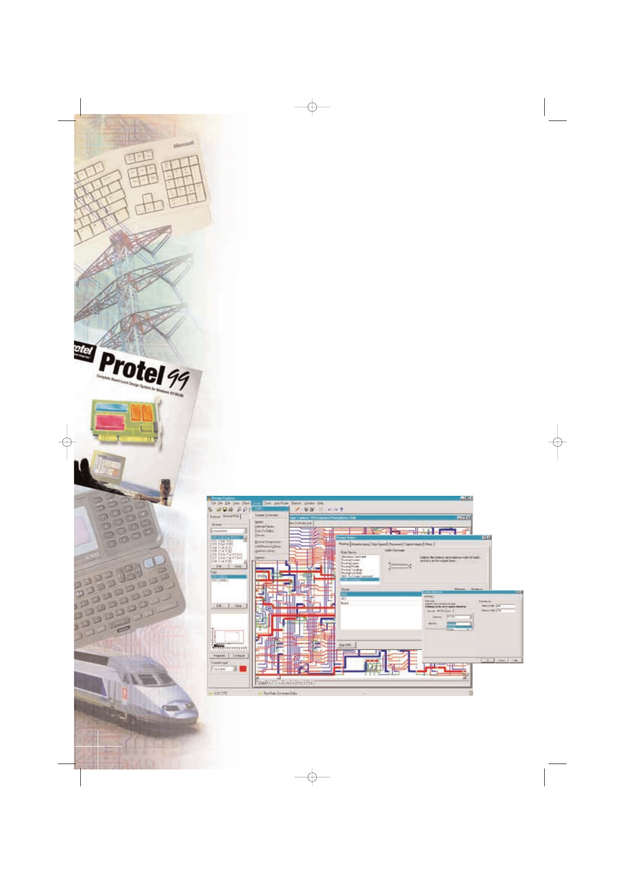
The PCB’s special “electrical grid” feature snaps the cursor to valid electrical connection
points, regardless of the current routing grid setting. This makes it easy to route to
off-grid pads and tracks, enabling virtually gridless manual routing.
Protel 99’s “avoid obstacle” manual routing mode automatically clips the track you are
placing to avoid creating design rule violations. This makes it easy to “slam-and-jam”
tracks together while maintaining defined clearances.
PCB LAYOUT EDITOR
q3 catalog web english v2.qxd 9/7/99 10:55 AM Page 9
8
6
Bring a new approach to graphical
printed circuit board design with
Protel 99’s superb PCB editor. The
PCB editor combines manual and
automated design in an interactive
environment that supports both
the new user and the experienced
designer. The underlying PCB data
structure is tuned for speed, and a
set of powerful design rules gives
you total control over the design
parameters. Equipped with manual
and interactive features that make
it easy to layout and route the most
complex mixed-technology designs,
Protel 99’s PCB editor is the perfect
balance of power and control.
Comprehensive design
rules ensure your design
meets the specs
PCB design can be a minefield
of conflicting requirements.
High-speed logic and smaller, more
complex packaging technologies
place extreme demands on the PCB
designer. Net impedance, track
clearances, signal reflections, path
lengths, critical trace widths - all
these factors and many more need
to be carefully monitored and
controlled to produce a successful
board design. Protel 99’s powerful
rules-driven design approach leaves
you free to focus on laying out and
routing the board while your
critical design requirements are
automatically monitored and
managed by the system.
Protel 99’s PCB Editor incorporates
over 25 design rule classes covering
areas such as component placement,
critical-net trace widths, crosstalk
constraints, net impedance, signal
reflections, clearances, object geom-
etry, parallelism, routing priority and
routing topology. Combined with the
ability to create multiple rules, each
applying to particular objects, nets,
components, regions, or the whole
board, Protel 99 gives you total
control over the design process.
The ability to create compound rule
scopes allows you to precisely target
the objects a rule applies to. With
simple-to-construct compound scope
definitions you can route a net at
one width on the top layer, and a
different width on the bottom layer.
Or close the solder mask over the
vias on the bottom layer, but not
the top layer.
One-click PCB-to-schematic
design synchronization
Design is not a simple linear
process. Changes and updates are
often made throughout the design
cycle and it’s all too easy for the
final board layout to get out of step
with the original schematics. With
Protel 99’s easy-to-use Design
Synchronizer, keeping your
schematic and PCB documents
in complete harmony is a breeze.
Reflecting PCB changes back to
the schematic is as easy as pressing
a button.
The Design Synchronizer analyzes
the source PCB document and target
schematic design to determine any
differences. If you have changed
component designators on your PCB
for example, the designators on the
schematic are automatically updated.
The Design Synchronizer can be
run at any stage in the board layout
process to ensure the total integrity
of your design documentation. With
Protel 99’s Design Synchronizer
technology you'll have complete
confidence that your schematic and
PCB documents represent the same
circuit throughout the design
process.
Intuitive editing environ-
ment = ease of design
Protel 99’s PCB editor is based on
familiar Windows-based graphical
editing techniques to make PCB
design a natural and intuitive
Powerful rules-driven design accelerates
Visit www.protel.com For more product information.
Protel 99’s PCB Editor incorporates over 25 design rule classes covering areas such as routing, manufacturing,
high-speed design, component placement, and signal integrity. Combined with the ability to create multiple rules,
each with a different scope, Protel 99 gives you total control over the design process. The ability to create
compound rule scopes allows you to precisely target the objects a rule applies to.
q3 catalog web english v2.qxd 9/7/99 11:08 AM Page 8

9
7
place components grouped first by
connectivity (creating clusters of
components), then by the component
geometry.
With higher component counts,
Protel 99’s Statistical Placer uses
an AI-based methodology called
“simulated annealing”. It analyzes
the entire design during placement,
considering the connection length,
the connection density on the
board, and the alignment of the
components, all in accordance
with the specified design rules.
Smart interactive placement tools
make short work of manual
placement jobs. Use the Auto Select
placement mode to quickly ‘collect’
components with similar footprints,
then rotate, expand and contract the
entire group as you move them to
the required location on the board.
Once your rough placement is
complete, use Auto Align mode to
neatly expand or contract a group
of placed components with similar
footprints. These and many other
advanced interactive features make
component placement in Protel 99
a designer’s dream.
Effortless interactive
manual routing
A major challenge for today’s PCB
designer is working with a mix of
imperial and metric technologies.
Protel 99’s powerful manual routing
features let you easily route to any
object on the board, regardless of
its placement grid.
process. Click-and-drag to move
or resize graphical objects and
double-click on an object to edit its
properties. If you’ve ever used any
Windows graphics editing packages
you’ll feel right at home with
Protel 99. Whether you’re a beginner
or a power user, Protel 99’s intuitive
interface gives you easy control
over a powerful set of PCB editing
features.
Versatile global editing features let
you apply property changes across
any set of objects throughout your
design. Double-click on a string
on the overlay to change its height,
for example, and you can instantly
apply the height change to the single
string, all strings on the overlay
layer, all strings throughout the
design, or any subset of strings
you define. Global editing makes
board-wide design changes easy.
And with Protel 99’s Slider Hand,
moving around your PCB design
has never been easier. Simply click-
and-hold the right mouse button
anywhere in the PCB workspace and
use the Slider Hand to ‘slide’ around
your view of the PCB. Combined
with automatic document panning
and hotkey zoom control, the Slider
Hand makes it easy to get the right
view of your design.
Feature Highlights
Powerful rules-driven
design environment with
comprehensive design rule
checking, including on-line
DRC for monitoring rule
violations as you work
Compound, hierarchical
design rule scopes that
enable you to specifically
target rules
Direct “one-button”
schematic-to-PCB and
PCB-to-schematic design
synchronization
State-of-the-art manual
and interactive routing
functions, including
“look ahead” track
placement for easy angular
and off-grid routing
Intelligent software “robot”
technology continually
monitors and updates
connectivity information
as you route
Sophisticated gridless
manual routing, with auto-
clipping and automatic
“snapping” of the cursor
to valid electrical hot spots
Push-and-shove manual
routing mode with full
design rule adherence
Intelligent polygon planes
(copper shielding) facility
with full DRC and
automatic connection
support
Full split power plane
support
3D board visualization with
automatic component
modeling - no additional
component height
information required
Automatic and interactive
component placement
features
Powerful global editing
features
Bi-directional crossprobing
to other documents,
including schematics,
reports and BOM’s
Continued ...
board layout
Contact your local sales office today for your FREE Protel 99 30-Day Trial CD.
Unbreakable connectivity
Connectivity is the foundation of
PCB design, and with Protel 99’s
PCB editor net integrity is
paramount. Connectivity is
continually monitored and analyzed
as you route, with the status of
each net constantly updated. As
connections are completed, the
corresponding ratsnest line is
automatically erased. And because
connectivity is monitored in
“real time”, you can route a net
from any starting point – you’re not
constrained by the ratsnest connec-
tion order. The net connectivity will
automatically be updated to reflect
the current routing.
Also, Protel 99 monitors routing
design rules as you work, instantly
flagging design rule violations. With
Protel 99’s unbreakable connectivity
and online design rule checking your
routing will be fast, accurate and
complete.
Enhanced component
placement tools
Component placement is the key to
good board layout, and Protel 99’s
PCB editor is equipped with two
powerful automatic placement tools,
as well as a comprehensive set of
intelligent interactive placement
features.
For boards with a low component
count, choose Protel 99’s Cluster
Placer that uses a component
clustering algorithm to automatically
Effortlessly route through tight spaces
using the “push-and-shove” manual
routing mode. Existing tracks are
pushed out of the way in accordance
with all relevant design rules.
The PCB’s special “electrical grid” feature snaps the cursor to valid electrical connection
points, regardless of the current routing grid setting. This makes it easy to route to
off-grid pads and tracks, enabling virtually gridless manual routing.
Protel 99’s “avoid obstacle” manual routing mode automatically clips the track you are
placing to avoid creating design rule violations. This makes it easy to “slam-and-jam”
tracks together while maintaining defined clearances.
PCB LAYOUT EDITOR
q3 catalog web english v2.qxd 9/7/99 11:08 AM Page 9
10
10
8
Protel 99’s configurable Electrical
Grid snaps tracks to the center of
electrical hot spots on placed objects
as you route. This, combined with
Protel's Predictive Track Placement
feature, makes accurate routing to
off-grid components effortless.
Protel 99’s “slam-and-jam”
(Avoid Obstacle) manual routing
mode automatically clips tracks as
you route to prevent design rule
violations. In this mode you can
easily route dense board areas,
achieving minimal allowable
clearances for all objects regardless
of grid setting. And to get through
those tight spots, Protel 99’s new
Push-and-Shove routing mode
intelligently moves existing tracks
to make way for a new track, while
preserving design rule compliance.
For the ultimate in rerouting
and cleanup, Protel 99’s Loop
Removal feature automatically and
intelligently removes redundant
track segments as you work. Simply
reroute any portion of an existing
track and Protel 99 will automatical-
ly delete the unnecessary segments.
Seamless autorouter
integration
When it comes to autorouter
integration, Protel 99’s PCB editor
sets the standards. There’s no
configuration file editing or netlist
import/export, simply click a button
and Protel 99’s advanced
shape-based autorouter goes to
work directly on the PCB layout.
Because the autorouter works
directly in the PCB editing window,
you can stop the autorouter at any
time and instantly work manually on
your design. Protel 99’s PCB editor
makes the dream of one-button
autorouting a reality.
Expert Wizards at your
fingertips
Protel 99’s PCB Editor includes a
number of intelligent design Wizards
that step you through common
design tasks. For example, use the
Board Wizard to select from and
customize one of the many industry
standard board templates, or create
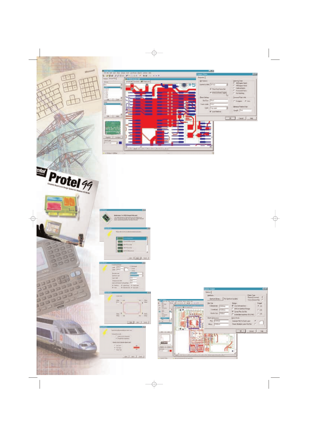
Protel 99’s PCB Editor includes
advanced polygon plane support.
Polygon planes can be placed on
any layer and assigned to any net.
Copper is automatically poured
around objects, observing all
relevant design rules.
Protel 99’s Board Wizard guides you
through the process of creating a new
board outline. Select from and customize
one of the many industry standard board
templates, or create your own custom
templates. The Board Wizard lets you
specify a title block, number layers, via
types, routing technology, default track
sizes and clearances, and many other
board parameters. The Board Wizard
then creates a new PCB document
complete with board outline and default
design rules.
Protel 99 provides
full output support
for Gerber RS274,
including support
for Gerber RS274X
embedded
apertures.
Visit www.protel.com For more product information.
q3 catalog web english v2.qxd 9/7/99 11:09 AM Page 10
9
with optional automatic connection
to a specified net. Polygon shapes
can be defined using line and arc
perimeters, and vertices can be
moved, added or deleted after
generation. Copper ‘pours’
automatically, observing all rules
and wrapping around all placed
objects, including arcs and non-
orthogonal shapes. Polygons can
be re-poured around new obstacles
and you can redefine the connected
pad relief styles at any time.
Bulletproof design verification
Make sure your board performs the
way you expect with Protel 99’s
comprehensive design rule checking
and reporting features. The batch-
mode Design Rule Checker (DRC)
thoroughly analyzes your design in
respect of all specified design rules.
A comprehensive DRC report flags
any design rule violations. Rule
violations are also highlighted
directly on the board to allow you
to easily focus on problem areas.
The DRC links directly to
Protel 99’s Signal Integrity Analyzer,
giving true verification of crosstalk,
reflection, impedance and other
signal integrity-related design rules.
Any violations of these rules
can be further investigated using
Protel 99’s integrated Signal
Integrity Simulator, which provides
comprehensive crosstalk and
impedance analyses, and
termination simulation.
With Protel 99’s design verification
features you can be confident in
your board’s performance before
it leaves your desktop.
Quickly and easily
create your own custom
component footprints
in Protel 99’s powerful
PCB Library Editor.
Using familiar PCB
design tools you can
create footprint designs
of any complexity,
allowing you to quickly
build custom component
libraries. With Protel 99,
you’ll never be stuck
without the right
footprint.
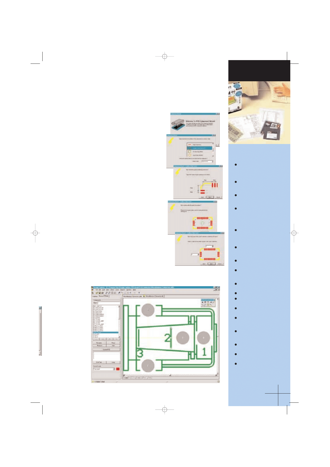
Protel 99’s Component Wizard generates
new PCB component footprints in no
time. Choose from a comprehensive
range of component types and
customize the important parameters of
your footprint in a set of easy-to-follow
steps. With Protel 99’s Component
Wizard, you’ll never be without a
crucial footprint again.
your own custom templates. The
Board Wizard lets you specify a
title block, number layers, via types,
routing technology, default track
sizes and clearances, and many other
board parameters. The Board Wizard
then creates a new PCB document
complete with board outline and
default design rules.
Building components is a breeze
with the Component Wizard. With a
few simple steps you can create any
component from a two-pin surface
mount resistor, right through to a
Pin Grid Array with several hundred
pins. The Component Wizard guides
you through every step in the
component creation process.
Easy component footprint
editing and management
Protel 99 comes with a comprehen-
sive array of PCB footprint libraries,
and new and updated libraries are
available for direct download from
Protel’s website at www.protel.com.
With Protel 99, you’ll have all the
component footprints you need at
your fingertips.
Protel 99 also includes integrated
component editing and library
management tools that make it easy
to create and organize your own
custom libraries. You can have any
number of libraries open at the same
time, and easily browse components
in open libraries.
Intelligent polygon planes
Protel 99’s PCB editor takes the
work out of generating polygon
planes. Solid or latticed polygon
planes can be placed on any layer,
32-bit design database,
providing a resolution of
0.001 mil in a 100x100
inch workspace
Full component rotation
with an angular resolution
of 0.001 degrees
16 signal layers, 4 power
planes and 4 mechanical
layers
Board creation Wizard
with industry-standard
board templates, and the
ability to define your own
board outline templates
Multiple library support
with no limit on the number
of libraries open at any
one time
Fully-featured footprint
library editor with
component creation Wizard
Automatic Gerber and
NC drill file generation
Import and export DXF and
AutoCAD DWG format files
up to and including R14
Full support for Windows
printer and plotter drivers
Unlimited Undo and Redo
Automatic positional
component re-annotation
Easy switching between
imperial and metric units
Export design objects to
spreadsheet for direct
property editing
Fully-customizable
toolbars, menus and
shortcut keys
Free hole size editor
add-on available
Free testpoint finder
add-on available
Free overlapping hole
detector add-on available
Feature Highlights
(continued)
Contact your local sales office today for your FREE Protel 99 30-Day Trial CD.
PCB LAYOUT EDITOR
q3 catalog web english v2.qxd 9/7/99 11:09 AM Page 11
12
10
3D board visualization mode
Why wait for your board to be
manufactured to see what it looks
like? Protel 99 includes sophisticated
3D board visualization technology
that lets you preview your
assembled board design as a
stunning 3D image. Run-time
component modeling techniques
automatically extrude and render the
components on your board without
the need to define additional height
information. Simply select the 3D
option from the PCB View menu
and your board will be instantly
brought to life.
You can render your board
populated, or hide the components
for a bare board view – very useful
for finding text over holes. You can
also show or hide the copper, text
and silkscreen layers, and even
highlight individual nets. You have
full rotational and zoom control over
the 3D image, so you can view your
board from any angle.
For unknown or custom board
elements, Protel 99’s 3D viewer
includes a simple 3D component
modeling language that allows you
to easily define an object’s extrusion
parameters.
Add a new dimension to your
board design with Protel 99’s
3D visualization technology.
Visit www.protel.com For more product information.
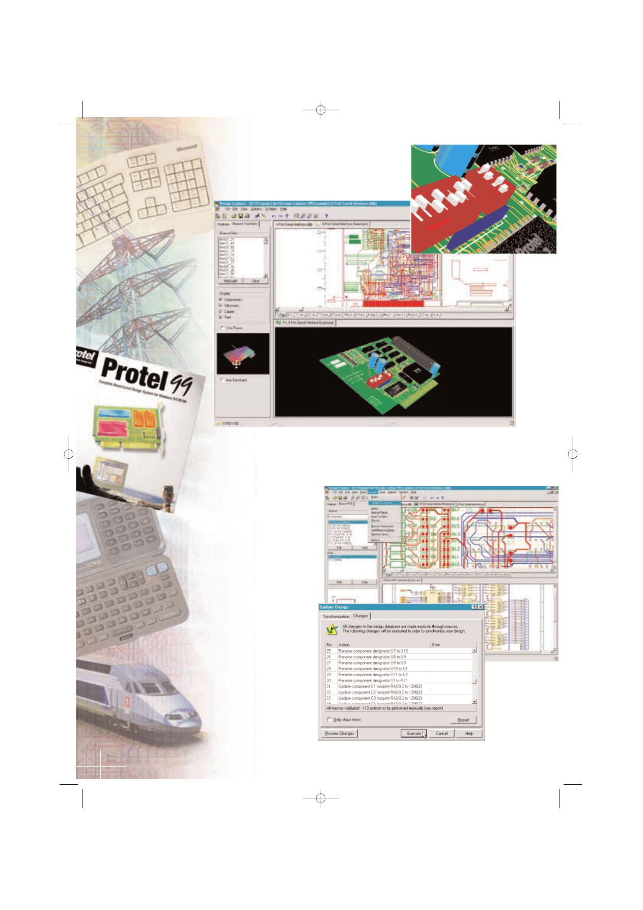
Protel 99’s unique 3D visualization feature lets you see your finished board
before it leaves your desktop. Sophisticated 3D modeling and extrusion
techniques render your board in stunning 3D without the need for additional
height information. Rotate and zoom to examine every aspect of your board,
and show or hide components, copper, silkscreen or text.
Reflecting modifications made on the PCB, such as designator and footprint changes,
is a simple one-step operation with Protel 99’s Design Synchronizer. No messing with
“Was-Is” files, simply run the Synchronizer at any time in the design process to make
sure your schematic and PCB documents are in perfect harmony.
q3 catalog web english v2.qxd 9/7/99 11:09 AM Page 12
13
11
Specifications
34 Layers: 16 x Signal;
4 x Mechanical; 4 x Internal Plane;
2 x Solder Mask; 2 x Paste Mask;
2 x Silkscreen; 2 x Drill
(Drill Guide & Drill Drawing);
1 x Keep Out; 1 x Multi-Layer
(spans all signal layers)
Max. board size:
100 x 100 inches
Max. Resolution:
0.001 mil linear displacement;
0.001o angular rotation
Import File Formats:
Netlist (Protel and Protel 2 formats);
AutoTrax; DOS PCB 3; AutoCAD
DXF; Gerber - batch or single;
Protel PCB 2.8 - ASCII and binary
Export File Formats:
Netlist (Protel format);
AutoCAD DXF; HyperLynx;
Protel PCB 2.8 - ASCII
Output Device Support:
Gerber RS274 (internal driver,
supports embedded apertures);
HPGL Plotter (internal driver);
all Windows printer & plotter drivers
Measurement Units:
Metric and Imperial
Max. Net Count: Unlimited
Report Generation:
Board Information Summary;
Selected Pins; Bill Of Materials;
Design Hierarchy; Netlist Status;
Signal Integrity; NC Drill (Excellon
binary and ASCII); Pick and Place;
Create Netlist (from copper)
Pads Styles:
Round; Rectangular; Octagonal
Pad Size:
0.001 to 99999 mils
Pad Stacks:
Different shapes definable for top,
bottom and mid layers
Via Styles:
Through-hole;
Blind & Buried (Layer Pairs);
Blind & Buried (Any Layers)
Track Widths:
0.001 to 99999 mils
Track Placement Modes:
Oblique; 45o; 45o with arcs;
90o; 90o with arcs
Interactive Routing Modes:
Ignore Obstacles; Avoid Obstacles;
Push-and-Shove
Polygon Plane Styles:
90o hatched; 45o hatched; Vertical
hatch; Horizontal hatch; Solid
Plane Connectivity:
Assignable to any net
Power Planes:
All plane layers can be assigned to
any net. All plane layers can have
multiple splits
Max. Components Per Board:
Unlimited
Max. Pins Per Component:
Unlimited
Max. Components Per Library:
Unlimited
Max. Simultaneously Open
Libraries: Unlimited
Contact your local sales office today for your FREE Protel 99 30-Day Trial CD.
PCB LAYOUT EDITOR
Versatile output generation
Protel 99 provides full support for
industry-standard Gerber RS274 and
NC drill file generation to give max-
imum manufacturer compatibility.
Load manufacturer-specific aperture
files, or let Protel generate an
aperture table from your current
PCB design. Protel supports
embedded apertures using the
Gerber RS274X standard.
And to complete your design
documentation, Protel 99 supports
all Windows printer/plotter drivers.
Print or plot your board layer-by-
layer, or create composite print outs
of all or selected layers.
Protel 99 leads the field for fast,
efficient, intelligent desktop
PCB design.
Spreadsheet export for
fast PCB object editing
Protel 99 includes a powerful PCB -
spreadsheet editing feature that gives
you a different perspective on your
design. An easy-to-use Spreadsheet
Export Wizard guides you through
the process of exporting selected
PCB object types. All objects of
the types defined, along with their
properties, are then displayed
in Protel 99’s integrated Excel-
compatible spreadsheet editor.
Use powerful spreadsheet editing
functions to view and edit the
properties of your PCB objects.
Search and replace component
designators, reassign polygon layers
– edit virtually any property of any
object on your board. When you’re
finished simply update the PCB
from the spreadsheet and your
changes are incorporated into
the PCB document.
Protel 99’s versatile spreadsheet
export feature gives you fine control
over your design objects and allows
you to view your design in an
entirely different way. It’s just
one more feature that makes PCB
design with Protel 99 easy.
Bi-directional AutoCAD
interface
Need to give your mechanical
designers a board outline in
AutoCAD format? No problem with
Protel 99’s bi-directional AutoCAD
interface. You can import or export
both DXF and native DWG files
directly from Protel 99’s PCB
Editor, making mechanical design
easier. The interface supports all
AutoCAD versions up to Release
14. User-definable layer mapping
allows you to easily relate PCB and
AutoCAD layers, and there is full
PCB component – AutoCAD block
conversion support. There is also
support for ungrouping components
during translation and displaying
rounded track ends in AutoCAD.
Protel 99’s powerful AutoCAD
translator takes the work out of
mechanical design issues.
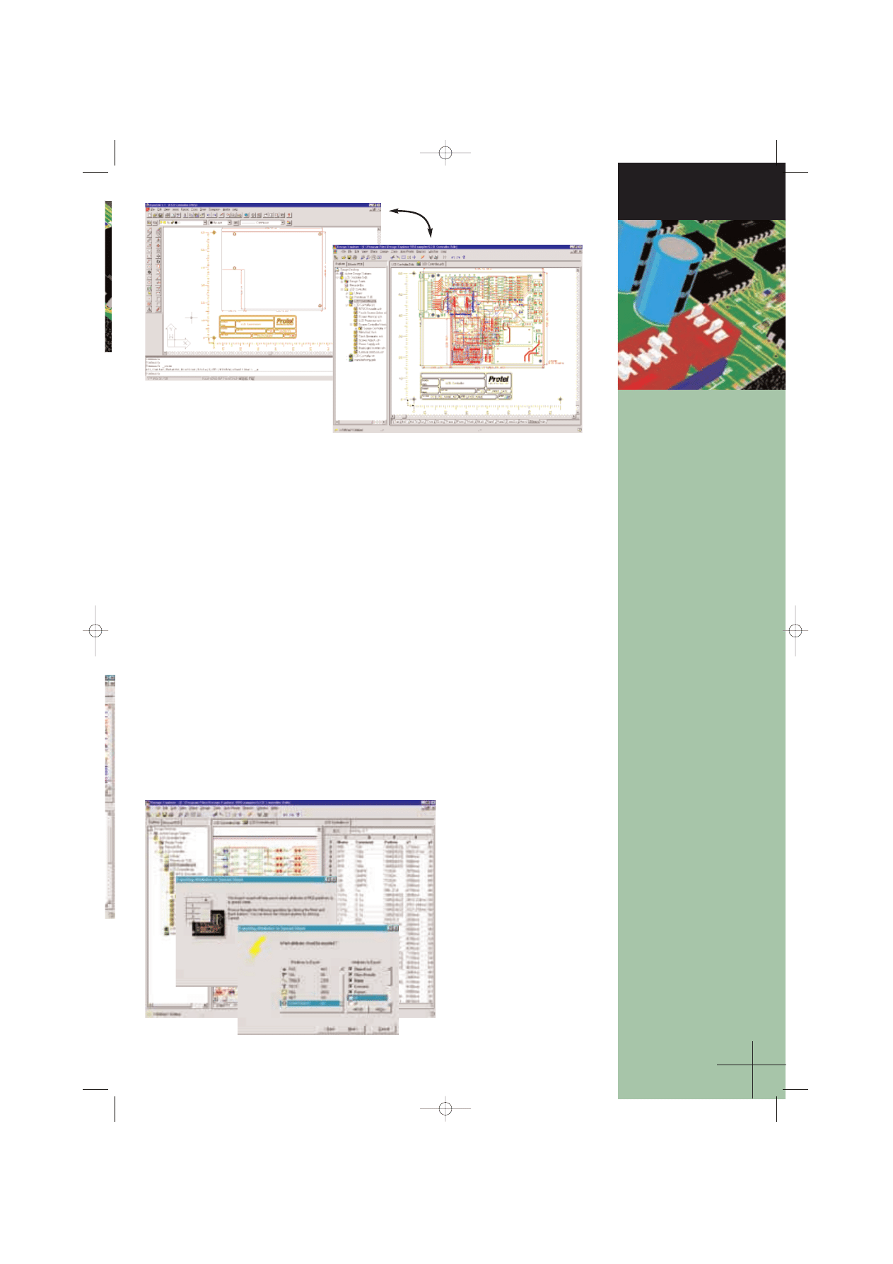
Easily export PCB design objects
to Protel 99’s Excel-compatible
spreadsheet editor using the PCB
spreadsheet Wizard. Design object
properties can be viewed and
edited using powerful spreadsheet
functions and features, and any
changes used to update the
PCB document. Protel 99’s PCB
spreadsheet export feature gives
you a whole new perspective on
your design.
Effortlessly interface from Protel 99’s PCB Editor
to AutoCAD drawings. Whether you want to import
a mechanical outline drawing to use as the board
boundary in Protel, or export your Protel board to
AutoCAD, Protel 99’s AutoCAD translator makes it
easy. The translator imports/exports both DXF and DWG files, as well as supporting
user-defined layer mapping and PCB component – AutoCAD block transforms.
q3 catalog web english v2.qxd 9/7/99 11:09 AM Page 13
Wyszukiwarka
Podobne podstrony:
PCB layout tuner layout for H LCD2005 from KTV on 5Jun
high speed usb pcb layout recom Nieznany
Engineering pcb(ebook PDF) WinBoard PCB Layout Reference Guide
Iphone 5 PCB Layout
PCB Layout Design Guide for Analog Applications
PCB layout tuner layout for H LCD2005 from KTV on 5Jun
17V 10A Switch Mode Power Supply (PCB layout) 020054 3
PCB printout (2)
PCB strzałka
Przedwzmacniacz Stereo z Regulacją Tonów, pcb 3xna stronie
PCB printout (2)
layout mockup
PCB Montaż
LCD F PCB
H BRIDGE PCB
opis PCB
PCB printout (3)
więcej podobnych podstron