
Ivex Design International, Inc.
WinBoard
®
PCB Layout
Reference Guide
Password Registration Number

ii
Copyright
1994-2000 Ivex Design International, Inc. All Rights reserved.
No part of this publication may be reproduced, translated into another language, stored in a
retrieval system, or transmitted, in any form or by any means, electronic, mechanical,
photocopying, recording, or otherwise without the prior written consent of Ivex Design
International, Inc.
Every precaution has been taken in the preparation of this publication. Ivex assumes no
responsibility for errors or omissions. Neither is any liability assumed for damages resulting
from the use of the information contained herein.
Ivex
is a trademark of Ivex Design International, Inc.
WinBoard®, WinDraft® and WinRoute® are registered trademarks of Ivex Design
International, Inc.
Ivex View and Ivex Spice are trademarks of Ivex Design International, Inc.
Specctra® is a registered trademark of Cooper & Chyan Technology, Inc. and Cadence Design
Systems.
Windows
is a trademark of Microsoft Corporation.
Microsoft® is a registered trademark of Microsoft Corporation.
1
All other brand and product names mentioned herein are used for identification purposes only,
and are trademarks or registered trademarks of their respective holders.
Document Number: PA1050.3
1
Microsoft is a registered trademark and Windows and the Windows Logo are trademarks
of Microsoft Corporation.

iii
Ivex Design International, Inc.
15232 NW Greenbrier Parkway
Beaverton, Oregon 97006-5746 U.S.A.
Sales & Administration
(503) 531-3555
Technical Support
(503) 531-9443
Bulletin Board System
(503) 645-0576
FAX
(503) 629-4907
General e-mail
info@ivex.com
Technical Support e-mail
help@ivex.com
World Wide Web
http://www.ivex.com

iv
LICENSE AGREEMENT
THE ENCLOSED SOFTWARE PROGRAMS ARE LICENSED BY IVEX TO CUSTOMERS FOR
THEIR NON-EXCLUSIVE USE ON A COMPUTER SYSTEM PER THE TERMS SET FORTH
BELOW.
DEFINITIONS:
"Ivex" shall mean Ivex Design International, Inc., which is the owner of the copyright and
author of this program. "Licensee" shall mean the end user of this Ivex Software. This Software Package
consists of copyrighted computer software and copyrighted user guide ("User Guide") from Ivex.
LICENSE:
We grant licensee a limited, non-exclusive license (i) to load a copy of the Software into the
memory of a single (one) computer as necessary to use the Program, and (ii) to make one (1) backup or
archival copy of the Software for the use with the same computer. The archival copy and original copy of
the Software are subject to the restrictions in this Agreement and both must be destroyed if your continued
possession or use of the original copy ceases or this Agreement is terminated.
RESTRICTIONS:
Licensee may not sub license, rent, lease, sell, pledge or otherwise transfer or distribute
the original copy or archival copy of the Program or the User Guide. You agree not to translate, modify,
disassemble, decompile, reverse engineer, or create derivative works based on the Software or any portion
thereof. Licensee also may not copy the User Guide. The Agreement automatically terminates without
notice if any provision of this Agreement is breached by Licensee.
LIMITED WARRANTY:
Ivex warrants that it has the right to license the Software to licensee.
Ivex warrants that the media on which the Software is furnished will be free from defects in materials and
workmanship under normal use for a period of ninety (90) days from the date of purchase. Ivex’s entire
liability and your exclusive remedy shall be the replacement of the Software if the media on which the
Software is furnished proves to be defective. This warranty is void if the media defect has resulted from
accident, abuse, or misapplication.
DISCLAIMER:
Except as provided above, the Software is provided "AS IS" without warranty of any
kind.
LIMITATION OF LIABILITY:
THE ABOVE WARRANTIES ARE THE ONLY WARRANTIES OF
ANY KIND, EITHER EXPRESS OR IMPLIED, INCLUDING WARRANTIES OF
MERCHANTABILITY OR FITNESS FOR ANY PARTICULAR PURPOSE. NEITHER Ivex, NOR ITS
VENDORS SHALL BE LIABLE FOR ANY LOSS OF PROFITS, LOSS OF USE, INTERRUPTION OF
BUSINESS, NOR FOR INDIRECT, SPECIAL, INCIDENTAL, OR CONSEQUENTIAL DAMAGES OF
ANY KIND WHETHER UNDER THIS AGREEMENT OR OTHERWISE.
EXPORT:
This Software is subject to U.S. Commerce Department export restrictions, and is intended for
use in the country into which Ivex sold it.
TERMINATION:
Ivex may terminate this license at any time if licensee is in breach of any of its terms or
conditions. Upon termination, licensee will immediately destroy the Software or return all copies of the
Software to Ivex along with any copies licensee has made.
APPLICABLE LAWS:
This Agreement is governed by the laws of the state of Oregon in the United
States of America, including patent and copyright laws. The prevailing party in any action or proceeding
brought in connection with an alleged breach of this Agreement shall be awarded reasonable attorneys’ fees
to be paid by the other party. This Agreement will govern any upgrades, if any, to the program that you
receive and contains the entire understanding between the parties and supersedes any proposal or prior
agreement regarding the subject matter hereof.

Contents
LICENSE AGREEMENT .............................................................................................IV
FORWARD.....................................................................................................................XI
M
INIMUM REQUIREMENTS TO RUN
W
IN
B
OARD
............................................................
XII
CHAPTER 1: EDITING FEATURES........................................................................... 1
S
ELECTING
O
BJECTS
....................................................................................................... 1
Selection Feature ....................................................................................................... 1
Selecting Blocks of Objects........................................................................................ 2
Selecting Modules ...................................................................................................... 3
Selecting Part of a Module ........................................................................................ 3
Selecting Objects Other Than Modules ..................................................................... 3
M
OVING
O
BJECTS
........................................................................................................... 4
E
DITING
T
RACKS
............................................................................................................ 5
Moving a Whole Track............................................................................................... 5
Dragging a Single Vertex of a Track ......................................................................... 5
Deleting a Vertex from a Track ................................................................................. 6
Adding a Vertex to a Track ........................................................................................ 6
Dragging a Single Track Segment ............................................................................. 7
Dragging Three Track Segments Simultaneously ...................................................... 7
Dragging a Whole Track ........................................................................................... 8
Flipping a Single Track Segment to Another Layer................................................... 8
E
DITING
Z
ONES
............................................................................................................. 12
Routing Tracks Through Zones................................................................................ 13
Selecting Zones ........................................................................................................ 13
Editing Zone Shapes ................................................................................................ 14
Editing Zone Characteristics ................................................................................... 14
Editing object in a zone ........................................................................................... 15
E
DITING
O
BJECTS
......................................................................................................... 15
R
OTATING
O
BJECTS
...................................................................................................... 16
F
LIPPING
M
ODULES
....................................................................................................... 16
M
OVING A
B
LOCK OF
O
BJECTS FROM
O
NE
L
OCATION TO
A
NOTHER
............................. 17
E
DITING
P
AD
S
TACKS
................................................................................................... 18
Selecting a Pad Stack to Edit................................................................................... 19
Editing Pad Shapes.................................................................................................. 19
Creating a New Pad Stack ....................................................................................... 20
Editing the Drill Hole Size....................................................................................... 21
Deleting a Pad Stack ............................................................................................... 21
Assign a Pad Stack to a Pad .................................................................................... 22

vi
U
NDO
........................................................................................................................... 22
CHAPTER 2: MENU REFERENCE .......................................................................... 23
F
ILE
.............................................................................................................................. 23
Loading Netlists ....................................................................................................... 25
Changing Module or Library Names....................................................................... 28
Update Netlist .......................................................................................................... 32
Printing and Plotting ............................................................................................... 35
E
DIT
.............................................................................................................................. 42
Selecting Objects ..................................................................................................... 42
Block Cut ................................................................................................................. 43
Block Copy............................................................................................................... 43
Block Paste .............................................................................................................. 43
Delete....................................................................................................................... 44
Select All .................................................................................................................. 44
Find, Get & Place Module....................................................................................... 44
Global Edit .............................................................................................................. 46
Edit Netlist (Netlist On the Fly) ............................................................................... 49
Undo ........................................................................................................................ 54
V
IEW
............................................................................................................................ 54
Zoom in.................................................................................................................... 54
Zoom out.................................................................................................................. 55
Zoom Best ................................................................................................................ 56
Zoom Refresh Screen ............................................................................................... 56
P
LACE
........................................................................................................................... 57
Adhesive................................................................................................................... 57
BookMark ................................................................................................................ 58
Dimensioning........................................................................................................... 61
Module..................................................................................................................... 63
Mounting Hole......................................................................................................... 65
Pass Mark ................................................................................................................ 66
Track, Outline & Edge............................................................................................. 68
Target ...................................................................................................................... 75
Text .......................................................................................................................... 77
Zone ......................................................................................................................... 79
T
OOLS
.......................................................................................................................... 85
Options .................................................................................................................... 85
Density Map............................................................................................................. 94
AutoPlace ................................................................................................................ 98
AutoRoute ................................................................................................................ 99
Load Routed Board.................................................................................................. 99
Netlist....................................................................................................................... 99
More Connections.................................................................................................. 102
CAM .......................................................................................................................... 102
Photo Plot.............................................................................................................. 103
NC Drill ................................................................................................................. 111

vii
Pick & Place .......................................................................................................... 115
BOM....................................................................................................................... 119
In Circuit Test ........................................................................................................ 121
DRC ........................................................................................................................... 123
Mechanical DRC ................................................................................................... 123
On-Line Electrical DRC ........................................................................................ 131
DRC Error List ...................................................................................................... 131
U
TILITIES
.................................................................................................................... 133
Statistics................................................................................................................. 133
Netlist Report ......................................................................................................... 134
Compare Netlists.................................................................................................... 135
Pin List Report ....................................................................................................... 138
Place File............................................................................................................... 139
Place File Report ................................................................................................... 140
Renumber Modules ................................................................................................ 141
W
INDOW
..................................................................................................................... 141
H
ELP
........................................................................................................................... 142
T
EMPLATES
................................................................................................................. 142
Save Template........................................................................................................ 143
Load Template ....................................................................................................... 143
CHAPTER 3: TOOLBARS........................................................................................ 145
M
AIN
T
OOLBAR
.......................................................................................................... 145
S
ECOND
T
OOLBAR
...................................................................................................... 146
L
AYER
N
UMBER
B
UTTONS
......................................................................................... 147
Routing layers (layer pairs) ................................................................................... 147
Disable layer.......................................................................................................... 148
S
CALE AND
U
NITS
....................................................................................................... 148
Scale....................................................................................................................... 149
Units....................................................................................................................... 149
Grid........................................................................................................................ 149
O
PEN
.......................................................................................................................... 150
S
AVE
........................................................................................................................... 150
Z
OOM
B
UTTONS
.......................................................................................................... 151
Zoom out ................................................................................................................ 151
Center Screen......................................................................................................... 152
Refresh Screen ....................................................................................................... 152
Zoom in .................................................................................................................. 152
Zoom Window ........................................................................................................ 152
Zoom to Fit ............................................................................................................ 153
CHAPTER 4: USING MODULE LIBRARIES........................................................ 155
C
REATING
M
ODULES WITH THE
M
ODULE
C
REATION
L
ANGUAGE
............................... 155
Module Creation Language Commands ................................................................ 156
Compiling and Decompiling (MCL and Module Libraries) .................................. 170
Examples of modules created with the Module Creation Language...................... 171

viii
G
RAPHICAL
M
ODULE
E
DITOR
..................................................................................... 178
Define New Module ............................................................................................... 179
Load Library Module............................................................................................. 181
Using the Module Editor ....................................................................................... 182
Example 1: Capacitor........................................................................................... 190
Example 2: Grid Array ......................................................................................... 191
CHAPTER 5: SPECCTRA INTERFACE ................................................................ 195
H
OW IT WORKS
........................................................................................................... 195
U
SING THE
I
NTERFACE
................................................................................................ 196
WinBoard to Specctra............................................................................................ 197
CCT Specctra to WinBoard (CCT2WB)................................................................. 203
T
UTORIAL
................................................................................................................... 205
A
DVANCED
U
SE
......................................................................................................... 206
Power Planes......................................................................................................... 206
L
IMITATIONS
............................................................................................................... 207
APPENDIX A: IMPORTING NETLISTS................................................................ 209
I
MPORTING AN
O
RCAD
S
CHEMATIC
N
ETLIST
.............................................................. 209
Installing the Orcad Interface ............................................................................... 209
Net Properties........................................................................................................ 211
Assigning Footprint Modules ................................................................................ 213
N
ETLIST
I
MPORT
: T
ANGO AND
P
ROTEL
...................................................................... 214
APPENDIX B: DRC DEFINITIONS ........................................................................ 215
D
RILL TO OTHER OBJECTS
........................................................................................... 215
Drill-Min./Max. ..................................................................................................... 215
Drill-Edge.............................................................................................................. 215
Drill-Pad................................................................................................................ 216
Drill-SMD.............................................................................................................. 216
Drill-Track............................................................................................................. 217
Drill-Via ................................................................................................................ 217
Drill-Drill .............................................................................................................. 218
V
IA TO OTHER OBJECTS
.............................................................................................. 218
Via Min./Via Max. ................................................................................................. 218
Via-Edge ................................................................................................................ 219
Via-Pad.................................................................................................................. 219
Via-SMD ................................................................................................................ 220
Via-Track ............................................................................................................... 220
Via-Via................................................................................................................... 220
T
RACKS TO OTHER OBJECTS
........................................................................................ 220
Track-Min./Track-Max. ......................................................................................... 221
Track-Edge ............................................................................................................ 221
Track-Pad .............................................................................................................. 221
Track-SMD ............................................................................................................ 222
Track-Track ........................................................................................................... 222

ix
SMD
TO OTHER OBJECTS
............................................................................................ 222
SMD-Min./SMD-Max............................................................................................. 223
SMD-Edge ............................................................................................................. 223
SMD-Pad ............................................................................................................... 224
SMD-SMD.............................................................................................................. 224
PAD
TO OTHER OBJECTS
............................................................................................. 225
Pad-Min./Pad-Max. ............................................................................................... 225
Pad-Edge ............................................................................................................... 225
Pad-Pad ................................................................................................................. 225
A
NNULAR
-M
IN
./A
NNULAR
-M
AX
. ............................................................................... 226
Z
ONE
.......................................................................................................................... 226
Zone-Min. .............................................................................................................. 226
APPENDIX C: KEYBOARD COMMANDS & EXTENSIONS .............................. 227
K
EY
C
OMMANDS
: ....................................................................................................... 227
F
UNCTION
K
EY
C
OMMANDS
....................................................................................... 229
N
UMERIC
K
EY
P
AD
C
OMMANDS
................................................................................. 229
S
CREEN
P
ANNING AND
Z
OOMING
K
EY
C
OMMANDS
.................................................... 231
O
BJECT
M
ANIPULATION
K
EY
C
OMMANDS
.................................................................. 231
L
IST OF
F
ILE
E
XTENSIONS
........................................................................................... 232
APPENDIX D: QUESTION/ANSWER..................................................................... 233
GLOSSARY.................................................................................................................. 236
INDEX........................................................................................................................... 249


Forward
This Ivex Users Manual contains detailed reference information about using
this product.
For information on getting started with this product, please refer to the
separate Getting Started Guide & Tutorial. The Getting Started Guide
contains the following information:
•
Introduction.
•
Installation and registration.
•
Minimum requirements.
•
How to reach Ivex and technical support.
•
Getting started using the program.
•
Tutorial.
•
Netlist information and how to go from schematic to PCB layout.
Registration and Pin Capacity
Some Ivex products install with a 100 pin capacity. Each user is assigned a
“personal” registration number. The user must enter their personal
registration number into the program to “enable” the pin capacity purchased.
Go to
Help | Registration
in the program and enter your personal
registration number, name and company in the space provided.
Usually the personal registration number is located in the front of the printed
manual or on the CD insert. If you have a disk version, it could be on the
back side of disk number one. For more detailed instructions, please refer to
the Getting Started Guide.

xii
Thank you for choosing Ivex. We hope you enjoy using this product. Please
remember to register your name, address, and e-mail number with Ivex so
that we can notify you of news and upgrades. News bulletins, tips and
notices of minor upgrades are sent electronically by e-mail and you may not
receive these unless you provide your e-mail address.
Minimum requirements to run WinBoard
To run WinBoard, you need the following:
Minimum Configuration
Preferred Configuration
486 DX 66 MHz CPU
Pentium CPU or greater
32 MB RAM
Over 64 MB RAM
20 MB hard disk space per program.
30 MB hard disk space per
program.
Color SVGA (800 x 600) display
with suitable Windows driver.
Color SVGA (800 x 600) display
with suitable Windows driver.
Windows 95b/98/NT4-SP4 or later.
Windows 95b/98/NT4-SP4 or later.
Mouse and CD Drive.
Note: newer versions of MS Windows require over 64 MB RAM just to load
the operating system. Make sure you have enough RAM to operate other
software applications.

Chapter 1: Editing Features
The Ivex interface has been designed so that most features can be quickly
reached with only a click or two of the mouse, or with a single keyboard
shortcut.
This chapter explains how to select, edit, rotate, and flip objects, how to
move objects from one location to another, and how to edit pad stacks.
Selecting Objects
This section explains how to select objects. Modules are selected differently
than other objects. The methods for selecting objects of any type are:
•
As blocks of objects
•
As single objects
Selection Feature
WinBoard allows the selection of objects in two ways as follows:
1.
Select and Move Off (not checked): Using this option, when you click
on an object and release the left mouse button the object will stay
selected. Then, move the mouse over the object to perform the desired
editing feature.
2.
Select and Move On (checked): Using this option, when you click on an
object you must hold the left mouse button down to keep it selected.
While holding the left mouse button down, drag the object or perform the
desired editing feature.
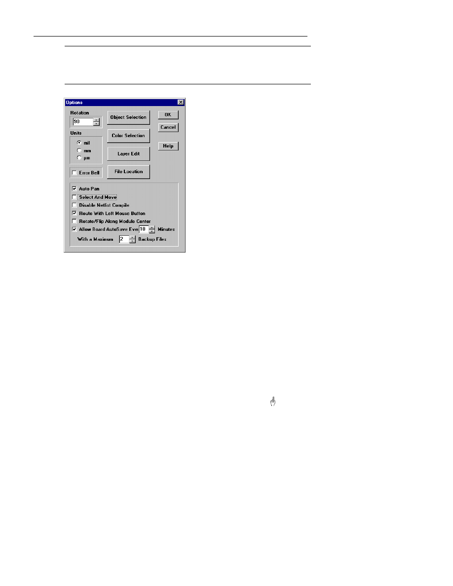
To change this selection method, use the Tools | Options dialog box and
choose the desired setting for the Select and Move feature.
:LQ%RDUG/D\RXW5HIHUHQFH*XLGH
2
F
NOTE: The Options dialog box is used to select a variety of user
preferences. It is a good idea to know the user options available in this
dialog box.
Figure 1-1. The Options dialog box.
Selecting Blocks of Objects
To select a block of objects, follow these steps:
1.
Place the pointer at one corner of the area you need to select.
2.
Press and hold the left mouse button while dragging the pointer to the
opposite corner of the area to be selected. WinBoard draws a dashed box
around the area that is selected.
3.
Release the left mouse button to complete the selection process. All
objects within the rectangle are now selected.
When you release the mouse button and whenever the pointer touches the
area surrounded by the rectangle, the pointer looks like this:
and the
Block Cut and Block Copy buttons display as active buttons rather than
dimmed buttons.

&KDSWHU(GLWLQJ)HDWXUHV
3
To cut or copy the block of selected objects, use the Block Cut and Block
Copy tools.
To move the block of selected objects, simply place the pointing hand
anywhere in the block and hold down the left mouse button while dragging
the block of selected objects.
Selecting Modules
To select a module, click the left mouse button on any pad that is part of the
module. WinBoard highlights the module.
Select more modules along with the one you have already selected by holding
down the
Ctrl
key while clicking with the left mouse button on a pad in
each module.
To unselect selected modules, click with the left mouse button on no object.
Selecting Part of a Module
With the exception of pads, to select any object that is part of a module, hold
down the
Ctrl
key while clicking with the left mouse button on the object
you want to select. Select more objects that are part of a module in the same
manner. For example, to select module text (Part Ref or Part Val) hold down
the
Ctrl
key and click on the text with the left mouse button.
To select the module outline, hold down the
Ctrl
key while clicking on the
outline with the left mouse button. To edit the outline, hold down the
Space
Bar
, this will allow you to insert and delete a vertex as you would when
editing a track.. When you are using the Module Editor it is not necessary to
use the space bar to edit the outline.
To select a pad that is part of a module, hold down the
Shift
key while
clicking with the left mouse button on the pad. To select more than one pad,
hold down on the
Ctrl
and
Shift
keys while clicking on the pads.
Selecting Objects Other Than Modules
The methods for selecting objects other than modules are:

:LQ%RDUG/D\RXW5HIHUHQFH*XLGH
4
1.
Select a single object by clicking on the object with the left mouse
button. WinBoard highlights the object.
2.
If you want to select more objects along with one you have already
selected, hold down the Ctrl key while clicking on each object.
F
NOTE: To unselect all objects, click again on another object or on no object.
Select T-Tracks
Hold down the
Ctrl
key and click on the track with the left mouse button.
This will select the track segment you clicked on and the adjoining T-Track
segment. The T-Track segment may be connected directly or with a via.
This enables you to move and drag adjoining segments.
Single track segments may be selected with a single mouse click and an
entire net may be selected using the net highlight (F5 key) function.
Moving Objects
This section explains how to move all objects other than tracks. For
information about moving and editing tracks, refer to Editing Tracks below.
To move any object other than a track, start by selecting the object. Notice
that as you move the pointer near the selected object, the pointer changes to
look like this:
. This pointer indicates that WinBoard has entered the mode
for moving objects. To move the selected object, follow these steps:
1.
Place the tip of the pointer finger on the object you want to move.
2.
Press and hold the left mouse button and drag the object to its new
location.
3.
Release the left mouse button. The object is no longer selected.
&KDSWHU(GLWLQJ)HDWXUHV
5
Editing Tracks
WinBoard provides powerful, flexible editing features that make it simple for
you to move a whole track, drag single vertices, delete single vertices, insert
new vertices anywhere on a track, drag a segment of track, drag three
adjacent track segments simultaneously, and drag a whole track without
moving the beginning and ending points. This section gives detailed
explanations of the WinBoard track editing features.
Moving a Whole Track
When moving a track, you need to know how the track move operation
works:
F
NOTE: If the track you want to move begins and ends on pads, the beginning
and ending points of the track will remain on the pads which retains net
connectivity. However, all ending points that are parked somewhere other
than a pad will move with the track.
Select the track you want to move by clicking on the track with the left
mouse button. Notice that as you move the pointer near the track, the pointer
changes to look like this:
. This pointer indicates that WinBoard has
entered the mode for moving tracks. To move an existing track, follow these
steps:
1.
Place the tip of the pointer finger on the track you want to move.
2.
Press and hold the left mouse button and drag the track to the new track
location.
3.
Release the left mouse button. The track is no longer selected.
Dragging a Single Vertex of a Track
Select the track you want to change by clicking on the track with the left
mouse button. Notice that as you move the pointer near a vertex of the
selected track the pointer changes to look like this:
. The
is used to
drag a vertex to a new location. To drag a vertex to a new location, follow
these steps:
:LQ%RDUG/D\RXW5HIHUHQFH*XLGH
6
1.
Place the
on the vertex you want to move.
2.
Press and hold the left mouse button and drag the vertex to the new
location.
3.
Release the left mouse button. The track remains selected so you can
perform more edits if you like.
Figure 1-2. The pointer used for dragging a vertex.
Deleting a Vertex from a Track
Select the track from which you want to delete a vertex. Notice that as you
move the pointer near a vertex on the selected track, the pointer changes to
look like this:
. The
is used to drag or delete a vertex. To delete a
vertex, follow these steps:
1.
Place the pointer on the vertex you want to delete. The pointer changes to
look like this:
.
2.
Press the
Del
key or click the right mouse button. The vertex is deleted.
The track remains selected so you can perform more edits if you like.
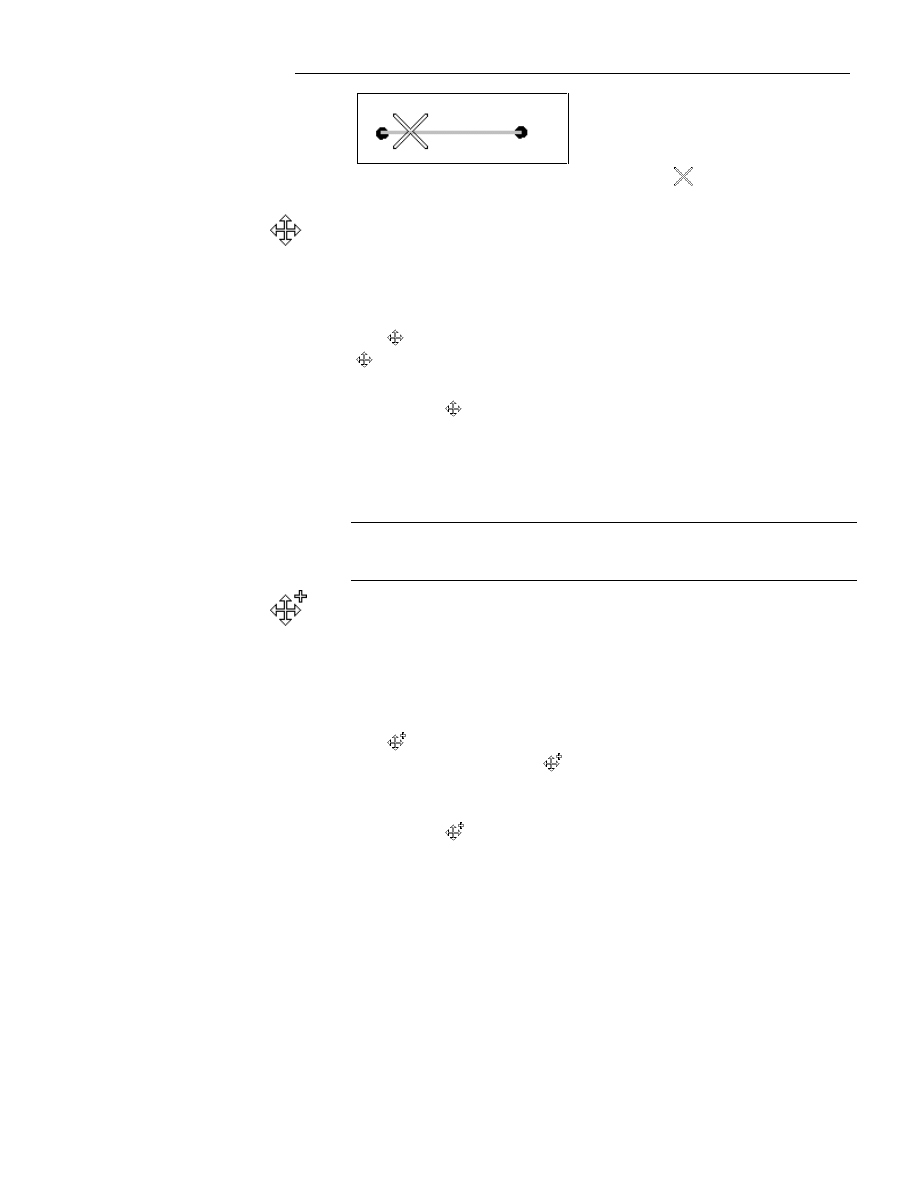
Adding a Vertex to a Track
Select the track to which you want to add a vertex. Notice that as you move
the pointer near a segment of the selected track the pointer changes to look
like this:
. The scissors are used to add a vertex to an existing track. To
add a vertex, follow these steps:
1.
Place the scissors at the location where you want to add a vertex.
2.
Click the left mouse button. The pointer changes from a scissors to look
like this:
.
&KDSWHU(GLWLQJ)HDWXUHV
7
Figure 1-3. The newly added vertex indicated by the
.
Dragging a Single Track Segment
Select the track you want to change by clicking on the track with the left
mouse button. Press and hold the
Ctrl
key. Notice that as you move the
pointer near a segment of the selected track the pointer changes to look like
this:
, signifying that WinBoard has entered the segment drag mode. The
is used to drag a single track segment to a new location. To drag a single
track segment to a new location, follow these steps:
1.
Place the
on the track segment you want to move.
2.
Press and hold the left mouse button and drag the track segment to the
new location.
3.
Release the left mouse button. The track remains selected so you can
perform more edits if you like.
F
NOTE: This method of dragging a track segment will only work for track
segments that have vertices in addition to a starting and ending point.
Dragging Three Track Segments
Simultaneously
Select the track you want to change by clicking on the track with the left
mouse button. Press and hold the
Shift
key. Notice that as you move the
pointer near a segment of the selected track the pointer changes to look like
this:
, signifying that WinBoard has entered the mode to drag three
adjacent track segments. The
is used to simultaneously drag three adjacent
tracks to a new location. Follow these steps to simultaneously drag three
adjacent track segments:
1.
Place the
on the center track segment of the three segments you want
to drag.

:LQ%RDUG/D\RXW5HIHUHQFH*XLGH
8
2.
Press and hold the left mouse button and drag the track segments to the
new location.
3.
Release the left mouse button. The track remains selected so you can
perform more edits if you like.
Dragging a Whole Track
To drag a whole track except for the beginning and ending points to a new
location, select the track you want to drag by clicking on the track with the
left mouse button. Press and hold the
Shift
and
Ctrl
keys. Notice that as
you move the pointer near the selected track the pointer changes to look like
this:
, signifying that WinBoard has entered the mode to drag a whole
track except for the beginning and ending points. The
is used to drag a
whole track except for the beginning and ending points to a new location.
To drag the track, follow these steps:
1.
Place the
on the track you want to move.
2.
Press and hold the left mouse button and drag the track to the new
location.
3.
Release the left mouse button. The track remains selected so you can
perform more edits if you like.
Flipping a Single Track Segment to Another
Layer
To flip a single track segment to another layer and insert vias, follow these
steps:
1.
Select the track with your left mouse button.
2.
Press and hold the
Ctrl
key.
3.
While holding the
Ctrl
key down, move the cursor over the track.
Notice that as you move the pointer near the selected track the pointer
changes to look like this:
, signifying that WinBoard has entered the
mode to flip a track segment.
4.
Now click the right mouse button to bring up the layer select box, and
choose which layer you would like to place the track on.
&KDSWHU(GLWLQJ)HDWXUHV
9
Flipping the Segment to a Lower Numbered Layer
To flip the track segment from the current layer to the next lower numbered
layer, select the track and then follow these steps:
1.
Hold the
Shift
key down while you place the
on the track segment
you want to flip to the next lower numbered layer.
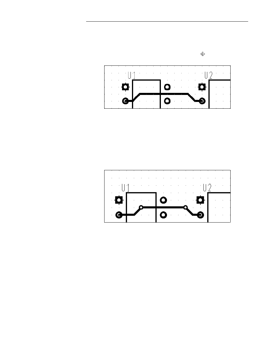
Figure 1-4. A track before the track segment is flipped.
2.
Press the
+ or -
key on the ten-key pad. WinBoard inserts a via at
each end of the track segment and the track segment changes color to
indicate it has moved to the next layer.
To continue moving the segment to lower numbered layers, continue
pressing
-
. The segment will continue changing layers until it wraps
back around to the component side.
3.
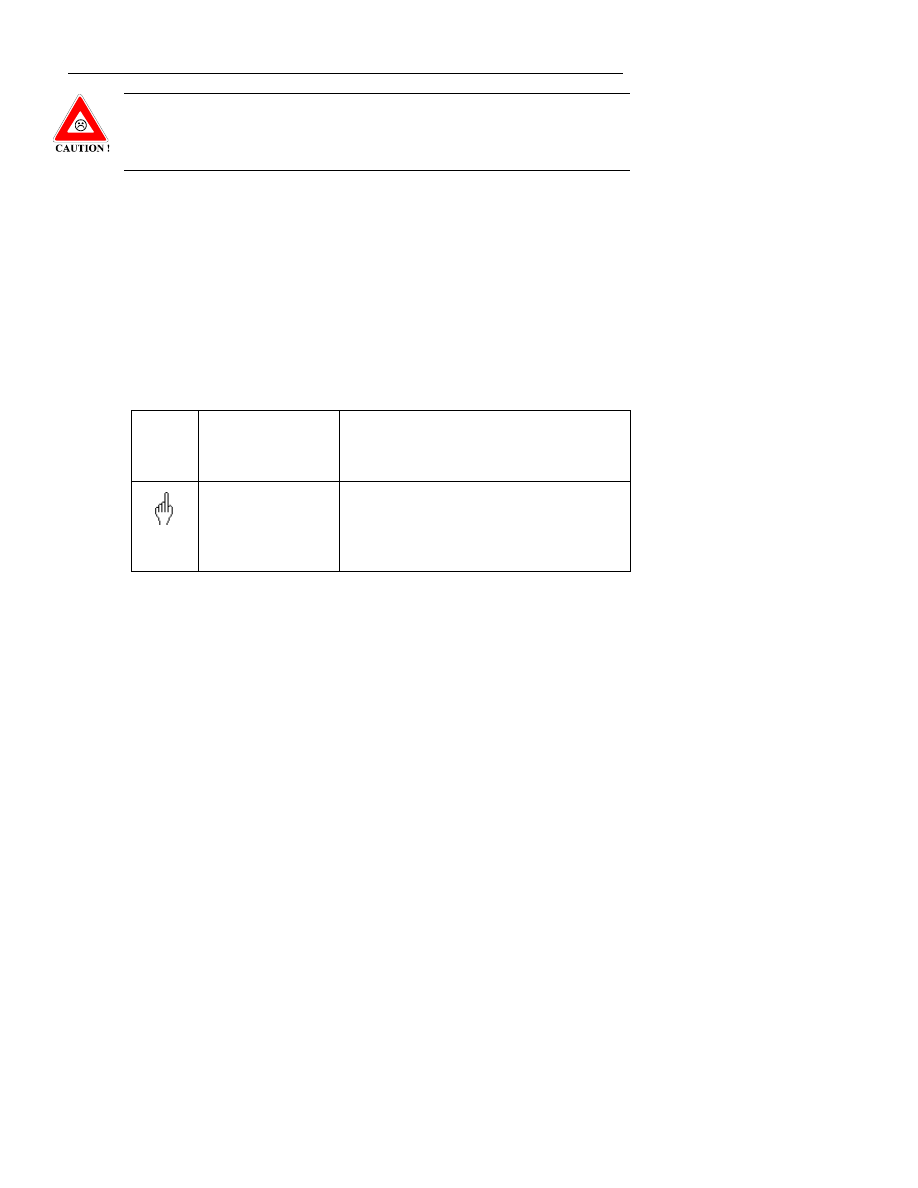
Unselect the track to complete the placement of the segment on the new
layer.
Figure 1-5. The same track as figure 1-4 after flipping a segment.
:LQ%RDUG/D\RXW5HIHUHQFH*XLGH
10
CAUTION: This will insert a via at both ends of the segment. Make sure this
is what you want to do. If the results are not what you intended, press the
Undo button.
Flipping the Segment to a Higher Numbered Layer
To flip the track segment from the current layer to higher numbered layers,
follow the steps in Flipping the Segment to a Lower Numbered Layer above
and use
+
instead of
-
to change layers.
If you continue pressing
+
, the segment will continue changing layers until it
wraps back around to the solder side.
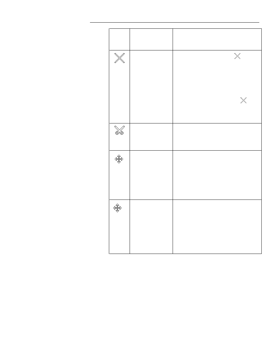
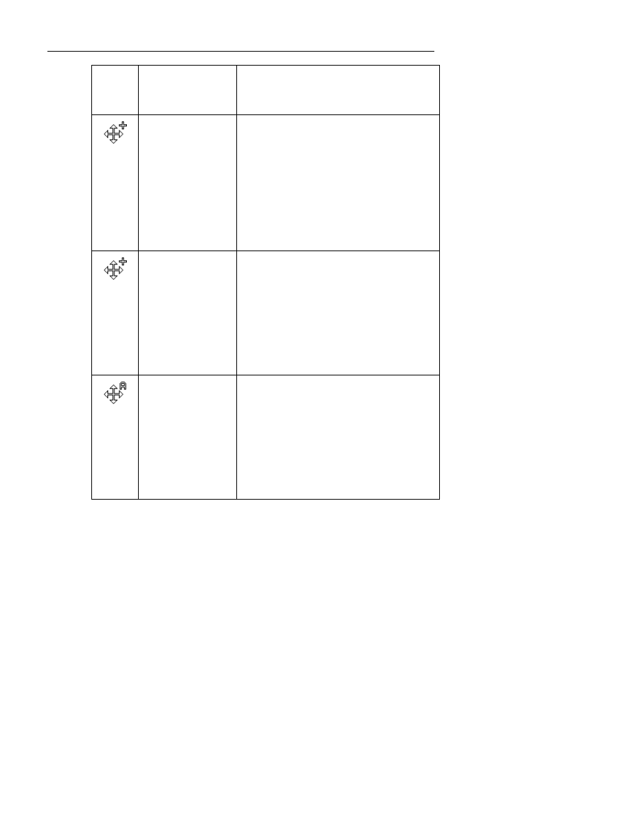
The following table summarizes the different pointers used for editing, the
action required to produce each pointer, and the use of each pointer.
Editing
Symbol
Action Required
to
Produce Symbol
Command Description
Move the pointer
near the selected
track.
Move objects: Place the pointing finger near
the selected track. Press and hold the left
mouse button while dragging the track to its
new location. Release the mouse button.
&KDSWHU(GLWLQJ)HDWXUHV
11
Editing
Symbol
Action Required
to
Produce Symbol
Command Description
Move the pointer
near any vertex of a
selected track.
Drag a single vertex: Place the
pointer
on the vertex of the selected track. Press and
hold the left mouse button while dragging the
vertex to its new location. Release the mouse
button. As you drag the vertex, the track
segments on either side of the vertex are
extended to maintain their original
connectivity.
Delete the single vertex: Place the
pointer on the vertex of the selected track and
press the
Del
key or press the right mouse
button.
Move the pointer
near a straight
segment of selected
track.
Insert a new vertex into the track at the
location of the scissors: Place the scissors on
the track segment where you want the new
vertex and click the left mouse button.
Press and hold the
Ctrl
key while
moving the pointer
near a single
selected track
segment.
Drag a single segment of track: Press and
hold the
Ctrl
key while placing the symbol
on the track segment to be moved and
clicking the left mouse button. Then drag the
segment to a new location and release the left
mouse button. The track segments on both
sides of the segment are extended to maintain
the original connectivity.
+
Press and hold the
Shift
key while
moving the pointer
near a single
selected track
segment and press -
.
Flip a single segment of track to the next
lower numbered layer and insert a via:
Press and hold the
Shift
key while placing
the symbol on the track segment to be moved
to another layer. Release the
Shift
key and
press -. Repeatedly pressing - will continue to
change layers until the solder side is reached.
Unselect track to complete placement of
segment on new layer.
:LQ%RDUG/D\RXW5HIHUHQFH*XLGH
12
Editing
Symbol
Action Required
to
Produce Symbol
Command Description
Press and hold the
Shift
key while
moving the pointer
near a single selected
track segment and
press
+
.
Flip a single segment of track to the next
higher numbered layer and insert a via:
Press and hold the
Shift
key while placing
the symbol on the track segment to be
moved to another layer. Release the
Shift
key and press
+
. Repeatedly pressing
+
will
continue to change layers until the
component side is reached. Unselect track to
complete placement of segment on new
layer.
Press and hold the
Shift
key while
moving the pointer
near the center
segment of three
adjacent track
segments.
Drag three adjacent track segments
simultaneously: Press and hold the
Shift
key while placing the symbol on the center
track segment and clicking the left mouse
button. Then drag the three segments to a
new location and release the left mouse
button. The track segments on both sides of
the segments being moved are extended to
maintain the original connectivity.
Press and hold the
Shift
and
Ctrl
Keys while moving
the pointer near a
track.
Drag a whole track except for the
beginning and ending points: Press and
hold the
Shift
and
Ctrl
keys while
placing the symbol anywhere on the track to
move and clicking the left mouse button.
Then drag the track to a new location and
release the left mouse button. The beginning
and ending track segments are extended to
maintain the original connectivity.
Editing Zones
WinBoard provides powerful, flexible editing features that make it simple for
you to edit zones. This section explains WinBoard’s zone editing features.
&KDSWHU(GLWLQJ)HDWXUHV
13
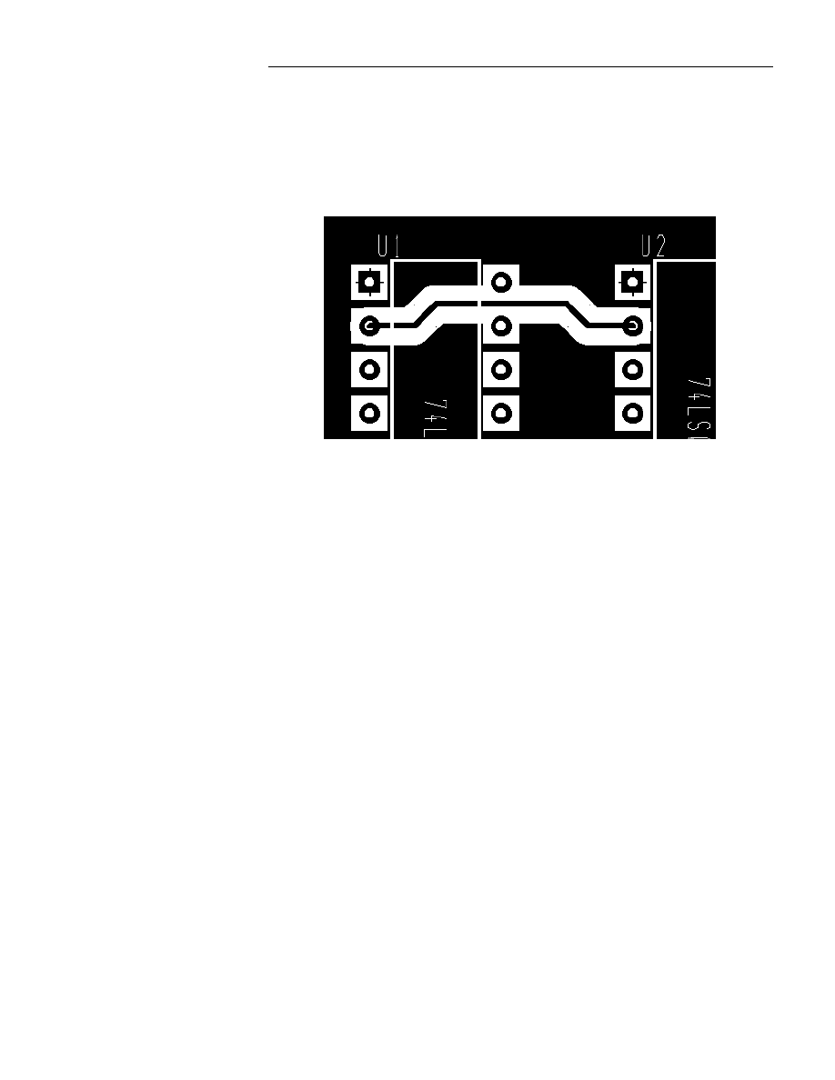
Routing Tracks Through Zones
Use the same method to route or edit a track belonging to a different net
through a zone as you would to route or edit any other track. After the track
is completely routed or edited, select and unselect the zone to redraw the
zone fill. The zone redraws the fill with the track isolated from the zone as
shown in Figure 1-6.
Figure 1-6. A zone with a track belonging to a different net.
Selecting Zones
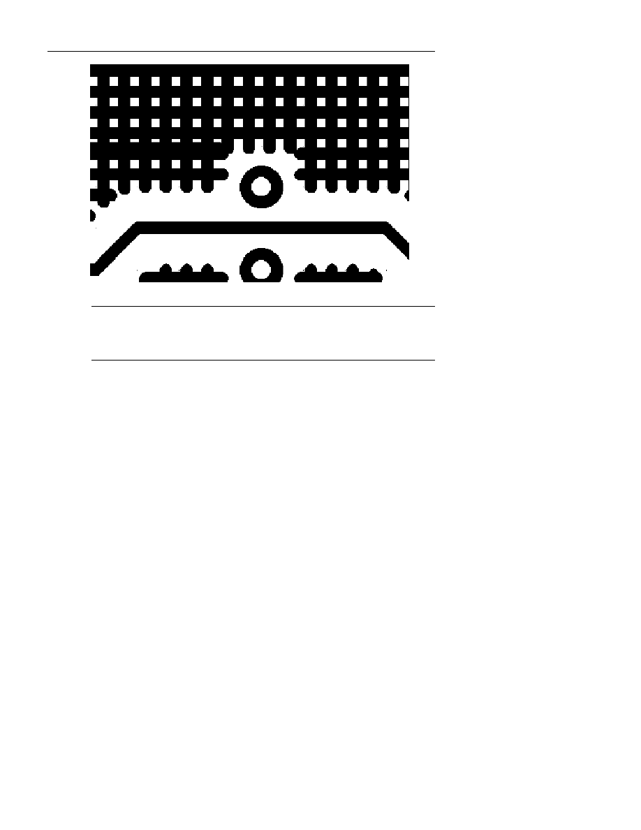
When you select a zone, make sure you click on part of the actual zone fill.
WinBoard fills zones with tracks. Depending on how dense you have made
the zone fill, it may be helpful for you to zoom in on the zone so you can see
where the zone fill tracks are before trying to select the zone. See figure 1-7.
:LQ%RDUG/D\RXW5HIHUHQFH*XLGH
14
Figure 1-7. Zoom in close to select track filling the zone.
F
NOTE: The smaller the zone grid size, the more time it takes WinBoard to
select a zone. There may be a slight delay before the zone displays as a
selected zone.
Editing Zone Shapes
To edit the shape of a zone, you need only select the zone you want to change
by clicking on the zone with the left mouse button, then use the same
procedures to edit the zone outline as you would use to edit a track.
To display the changes you have made to the shape of the zone, select the
zone by clicking on it with the left mouse button, then unselect the zone by
clicking on something other than the zone. WinBoard redraws the zone fill.
For more information about how to edit tracks, refer to the Editing Tracks
section above.
Editing Zone Characteristics
You can edit zone characteristics such as zone grid size, line width, and
thermal reliefs.

&KDSWHU(GLWLQJ)HDWXUHV
15
To edit zone characteristics, follow these steps:
1.
Double-click on the zone. The Zone dialog box displays. (Alternately,
you can single-click on the zone, then press F3 for the Global Edit dialog
box, then click on the Copper Zone button.)
2.
Change the zone characteristics in the Zone dialog box and click OK.
WinBoard displays the main WinBoard screen with the changes you
have made.
For more information about how to change the zone characteristics in the
Zone dialog box, refer to Chapter 2.
Editing object in a zone
To select objects within a zone, first de-select the zone. This turns off the
zone without deleting it and makes it possible to select objects without
selecting the zone.
1.
In the Setup menu, choose Object Select.
2.
In the Object Select dialog box, turn off Metal Zones.
3.
Press OK and exit the dialog box.
Now, the zone is not visible, but it is still there and you can easily click on
objects to select and edit.
Editing Objects
Editing any object other than a module is as simple as double-clicking on the
object with the left mouse button and selecting the appropriate characteristics
from a dialog box, then selecting OK.
For example, if you want to change a dimensioning arrow from external to
internal, follow these steps:
1.
Place the pointer on the dimensioning arrow you want to change and
double-click the left mouse button. The Dimensioning dialog box
displays.
2.
Click with the left mouse button on the Internal radio button and click
OK.

:LQ%RDUG/D\RXW5HIHUHQFH*XLGH
16
Rotating Objects
Before you try to rotate an object, make sure the rotation angle in the Tools |
Options dialog box has been set to the degrees you want to rotate objects.
To rotate an object around its reference point, follow these steps:
1.
Select the object.
2.
Rotate the objects clockwise by pressing the right arrow key, or
counterclockwise by pressing the left arrow key.
3.
Click with the left mouse button on no object to unselect the objects.
To rotate a block of objects around the center of the block, use the same steps
as for rotating an object around its reference point, but press
Ctrl
and the
left or right arrow key simultaneously.
Module rotation point
There are two things that determine the rotation point for modules. One is
the reference point of the module and the other is Rotate/Flip Along Module
Center user option located in the Tools | Options dialog box.
1.
When you create a module, the reference flag determines the point of
rotation. This flag is usually located at pin one, however it is often
placed at the center point of SMT modules.
2.
In the Tools | Options dialog box, you can select the feature Rotate/Flip
Along Module Center. Checking this option will rotate a module around
the center point even if the Reference flag is located on pin one.
Rotation Tip
When using the Place File feature, you should not select the Rotate/Flip
Along Module Center option because the Place File Report is generated
using the Reference Point of the module.
Flipping Modules
Modules can be flipped from the component side of the board to the solder
side and vice versa.
To flip a module or block of modules, follow these steps:

&KDSWHU(GLWLQJ)HDWXUHV
17
1.
Make sure no tracks are routed to the module or modules that will be
flipped.
2.
Select the module or block of modules.
3.
Flip the modules around the X axis by pressing the down arrow key. The
down arrow key works as a toggle, repeatedly flipping the modules up
and then down.
4.
Flip the modules around the Y axis by pressing the up arrow key. The up
arrow key works as a toggle, repeatedly flipping the modules left and
then right.
F
NOTE: Flipping an SMD module moves the module to the other side of the
board.
Modules with tracks attached will not flip.
5.
Click with the left mouse button on no object to unselect the modules.
To flip a block of modules along the center of the block, use the same steps
as for flipping an object around its grip point, but press
Ctrl
and the up or
down arrow key simultaneously.
Moving a Block of Objects from One Location
to Another
To move a block of objects from their current location to another location,
follow these steps:
1.
Select the block of objects.
2.
Place the tip of the pointer finger somewhere within the selected block of
objects.
3.
Press and hold the left mouse button.
4.
Drag the block to its new location and release the mouse button. The
block of objects unselects itself.
Move object to exact X,Y coordinates
Place the Reference Bookmark on an object to move it using exact x,y
coordinates. Example:

:LQ%RDUG/D\RXW5HIHUHQFH*XLGH
18
1.
Select the Reference Bookmark and place the bookmark on a track
vertex.
2.
Select the track using the block command. Notice that the x,y
coordinates turn RED rather than their usual black.
3.
Grab the block anywhere using the hand cursor. The coordinates will
only display the location of the Reference Bookmark no matter where
you grab the block.
4.
Move the object to the exact x,y coordinate.
Editing Pad Stacks
WinBoard allows differently shaped pads for Top, Internal, and Bottom
layers of the PC board by using pad stacks. Pad stacks are used to define all
pads. Each pad stack consists of one drill dimension—for through pads—and
a stack of pad shapes. When available routing space is at a minimum, you can
free up more room for routing by changing the size or shape of single pads on
the layers needing more room.
Use the Pad Stack Library to change or edit pad stacks.
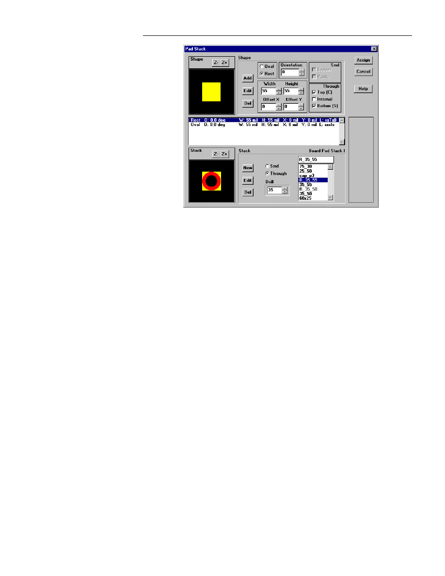
The Pad Stack Library dialog box is shown below :
&KDSWHU(GLWLQJ)HDWXUHV
19
Figure 1-8. Pad Stack dialog box.
Use Pad Stack Library to load or edit pad stacks that have been previously
defined and saved, and to save pad stacks that you want to save for future
use.
Selecting a Pad Stack to Edit
To edit a pad stack, use your mouse to double-click on a module’s pad. The
Pad Stack Library dialog box displays. To select an SMD pad, the current
layer must be the same layer as the module.
Editing Pad Shapes
To add a pad shape to the pad stack follow these steps:
1.
Set the Width, Height, Offset, and Orientation parameters in the Shape
section of the dialog box.
2.
Select Oval or Rect.
3.
Select layer options:
•
For SMD pads, use either Copper or Paste, or both.

:LQ%RDUG/D\RXW5HIHUHQFH*XLGH
20
•
For through pads, use Top, Internal, or Bottom, or any
combination.
4.
Click Add in the Shape section of the dialog box. The new shape is
added to the stack along with the pad’s description in the list box in the
center of the dialog box.
To Edit a pad shape in an existing pad stack follow these steps:
1.
Change the Width, Height, Offset, and Orientation parameters in the
Shape section of the dialog box.
2.
Select Oval or Rect.
3.
Select layer options:
•
For SMD pads, use either Copper or Paste, or both.
•
For through pads, use Top, Internal, or Bottom, or any
combination.
4.
Click Edit in the Shape section of the dialog box. The edited shape is
listed with the pad’s modified description in the list box in the center of
the dialog box.
To Delete a pad shape in an existing pad stack follow these steps:
1.
Click on the pad shape to delete in the list box in the center of the Pad
Stack Library dialog box. The selected shape becomes highlighted in
the list box and displays in the Shape view box.
2.
Click Del in the Shape section of the dialog box to delete the shape. The
shape is removed from the list box.
F
NOTE: Use the Z+ and Z- buttons to zoom in and out of the Shape and
Stack viewing windows.
Creating a New Pad Stack
To create a new pad stack, first give the pad stack a name as follows:
1.
Enter a new pad stack name in the Board Pad Stack List box.
2.
Click New in the Stack section.
Now enter a new shape in the Shape section of the dialog box as follows:

&KDSWHU(GLWLQJ)HDWXUHV
21
1.
Set the Width, Height, Offset, and Orientation parameters in the Shape
section of the dialog box.
2.
Select Oval or Rect.
3.
Select layer options:
•
For SMD pads, use either Copper or Paste, or both.
•
For through pads, use Top, Internal, or Bottom, or any
combination.
4.
Click Add in the Shape section of the dialog box. The new shape is
added to the stack along with the pad’s description in the list box in the
center of the dialog box.
5.
To create an SMD pad, click in the box next to Smd in the Stack section
of the dialog box.
To create through pads, click in the box next to Through Hole and select the
drill hole size in the box directly below the Smd / Through Hole buttons.
6.
Continue to add new shapes until the stack is complete.
Editing the Drill Hole Size
Use Edit in the Stack section of the dialog box to edit the drill hole in
through pads as follows:
1.
Double-click a through pad on the board.
2.
Change the Drill size in the box in the Stack section of the dialog box.
3.
Click Edit in the Stack section of the dialog box. The through pad
changes to the selected drill setting.
4.
Click Assign to replace the pads on the board.
Deleting a Pad Stack
To delete a pad stack, follow these steps:
1.
Click on a pad stack in the Board Pad Stack List box.

:LQ%RDUG/D\RXW5HIHUHQFH*XLGH
22
2.
Click Del. The pad stack is deleted. WinBoard will not delete a pad stack
that is in use. If you try to delete a pad stack that is in use, WinBoard
displays an error message.
Assign a Pad Stack to a Pad
Use Assign to assign a new pad shape to a pad stack.
F
NOTE: If you are editing a pad on the board, Assign replaces all pads on
the board using the same pad name. If you want to change only one pad,
create a new pad stack, then click Assign.
Use Cancel to exit the Pad Stack Library dialog box without saving any
changes and return to the main WinBoard screen.
Use Help to display online help. The Help tool works similarly to online help
in other Windows-based applications.
Undo
The Undo tool button is shown at left. When the Undo button is active,
you can undo commands by clicking once on the button. You can use
Undo to:
•
Undelete objects
•
Undo moves
Chapter 2: Menu Reference
This chapter describes the WinBoard menus. Menus are listed in the order
they display when WinBoard is running.
WinBoard uses ten pull-down menus: File, Edit, View, Place, Tools, CAM,
DRC, Utilities, Window, and Help. This section explains how each menu
works.
File
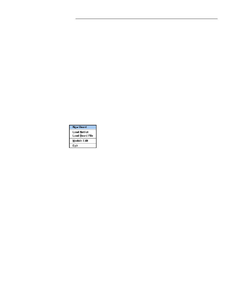
There are three different File pull-down menus, depending on whether you
already have at least one board file open, or you are opening a single board
file, or in the Module Editor (the Module Editor is discussed in Chapter 4).
When you are opening a single board file, File contains the menu
selections shown in the File pull-down menu at left.
Select New Board to start a new board file. The New Board dialog
box contains these options: Number of layers, Layer Edit, Design
Rules, and Setup. For more information about setting the New
Board options, see Running WinBoard in Chapter 2: Getting Started
with WinBoard, and Design Rules and Setup in the Toolbar section of
this chapter.
Select Load Netlist to load a netlist into a board file for the first time. Refer
to Loading Netlists just after the File menu description for more information
about how to load a netlist.
Select Load Board File to load an existing WinBoard board file.
Select Module Edit to load the module editor.
Select Exit to exit from WinBoard.

:LQ%RDUG/D\RXW5HIHUHQFH*XLGH
24
When you already have at least one board file open, File contains the
menu selections shown in the File pull-down menu at left.
Select New Board to start a new board file. The New Board dialog
box contains these options: Number of layers, Layer Edit, Design
Rules, and Setup. For more information about setting the New
Board options, see Running WinBoard in the Getting Started Guide,
and Design Rules and Setup in the Toolbar section of this chapter.
Select New Netlist to load a netlist into a board file for the first time. For
more information about how to load a netlist, refer to Loading Netlists,
immediately following the File menu description.
Update Netlist provides forward annotation to update existing net and
module characteristics from the schematic. For information about how to load
a netlist, refer to Loading Netlists, immediately following the File menu
description.
Select Load Board File to load an existing WinBoard board file.
Select Load Template to load an existing template file into a WinBoard
board file.
Select Save Board File to save the WinBoard board file on which you have
been working. Save Board File works similarly to the Save option in other
Windows-based applications.
Select Save Board File As to give a WinBoard board file a new name while
saving the board file. Save Board File as... works similarly to the Save As
option in other Windows-based applications.
Select Save Template to save all of the current WinBoard settings into a
template file. For more information about templates, refer to Chapter 2.
Select Module Edit to load the module editor. Refer to Chapter 3: Using
Module Libraries.
Select Close to close the current file.
Select Print to print or plot various layers of your board file. For more
information about printing and plotting, refer to Printing and Plotting, later
in this chapter.
Select Exit to leave the program.
&KDSWHU0HQX5HIHUHQFH
25
Loading Netlists
WinBoard has an advanced netlist loading interface that loads netlists from
various schematic programs and manually or automatically assigns module
names to the parts.
To load the netlist, follow these steps:
1.
In the File pull-down menu, click on either Load Netlist or New Netlist,
depending on which File menu displays. If you are opening a single
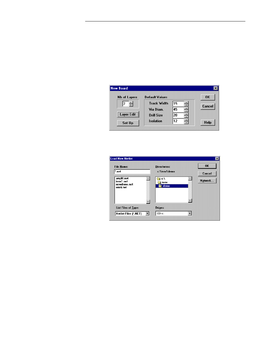
board file, the New Board dialog box displays as shown below :
Figure 2-1.. The New Board dialog box.
2.
Click OK to accept your changes to the New Board dialog box. The
Load New Netlist dialog box displays as shown below :
Figure 2-2. The Load New Netlist dialog box.
3.
Select the directory from which you would like the file loaded and the
file you want loaded and click OK. The netlist loader tries to detect the
format that was used to create the netlist you have chosen. The netlist
loader will find one of the following possibilities and act accordingly:
:LQ%RDUG/D\RXW5HIHUHQFH*XLGH
26
•
If the netlist is already in WinBoard format, the netlist loader begins
checking the netlist file for syntax errors.
•
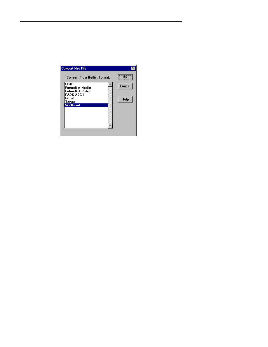
If the netlist is in a format other than WinBoard, the Convert Net
File dialog box displays as shown below. The highlighted format is
the format from which WinBoard will convert the netlist. If the
highlighted format is acceptable to you, click OK.
Figure 2-3. Convert Net File dialog box.
•
If WinBoard cannot recognize the format of your netlist file, it will
show the netlist format as UNKNOWN. If you are sure the netlist
format you tried to load is one of the supported netlist formats, click
on the correct netlist format and click OK.
When you click OK, the netlist loader begins checking the netlist file for
syntax errors. The netlist loader warns you when there is an error and
displays the line number where the problem was identified.
Some netlists require both a net file and a component file. If more than
one file is required, the netlist loader asks you to specify the component
file name in a standard Windows Open File dialog box.
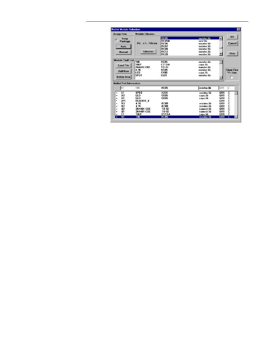
When the netlist is successfully converted, the Netlist Module Selection
dialog box displays as shown next :
&KDSWHU0HQX5HIHUHQFH
27
Figure 2-4.. The Netlist Module Selection dialog box.
The last list box in the Netlist Module Selection dialog box, referred to as
the Netlist Part Information list box, lists each part in the netlist and
characterizes each part from left to right by: Part Reference, Part Value,
Module Name, Library Name, Group Name, and Layer Name.
5.
Scroll through the Netlist Part Information list box. If all of the
modules look correct, click OK. WinBoard marks all the modules that
have incorrect module or module library names with an asterisk (*) in the
far left column of the Netlist Part Information list box. The netlist
loader finishes loading the netlist by placing the modules on the board
file, writes out a stuff file with the
.STF
file extension, and updates the
original netlist.
If your netlist was created with a netlist creation package for which
WinBoard supports automatic stuff back, the information from the
.STF
file
is also stuffed back into the schematic. This is how automatic stuff back
works:
WinBoard first checks to see if the netlist is a format that supports automatic
stuff back. If automatic stuff back is supported for your netlist, the netlist
loader prompts you for the root sheet of the design you would like the
module information merged back into. You can use the suggested file name
or use another file name, then click OK.

:LQ%RDUG/D\RXW5HIHUHQFH*XLGH
28
After the netlist loader finishes stuffing the information back into the
worksheet, it starts loading the modules into the WinBoard file.
If the schematic from which the netlist was generated was created with a
schematic creation package that does NOT support stuff back, but the
package allows the information to be entered into the schematic package,
then WinBoard does the following:
WinBoard checks to see if the schematic creation package supports a module
WAS_IS file. If a WAS_IS file is supported, WinBoard generates a WAS_IS
file in the format you select from a dialog box. If the schematic creation
package fails to support a module WAS_IS file, WinBoard generates a
WinBoard general WAS_IS file.
After the WAS_IS file is generated, the netlist loader starts loading the
modules into the WinBoard file.
Anytime the netlist loader needs to overwrite a current file, you are asked if
the netlister should overwrite the already existing file.
F
CAUTION
: For some netlist formats, the stuff back process accesses the
sheet files in binary format. If this process in some way fails—because of
incompatible sheet formats—the sheet database could be destroyed. We have
tried to avoid a situation like this. However, since we cannot control the
schematic editing packages, we cannot guarantee that your files will be
protected.
To make sure you can always recreate your sheet files, the stuff process
creates a
*.BAK
file for each of the schematic files to which data is written.
Changing Module or Library Names
If you want to change the module name or the library name of any of the
modules in the Netlist Part Information list box, you need to use some of
the features defined below:
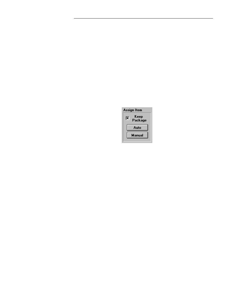
Use Assign Item Auto to have WinBoard automatically perform the
following steps:
1.
Assign library file names to those modules that have module names, but
no library names.
&KDSWHU0HQX5HIHUHQFH
29
2.
Try to match Part Values from the center list box—referred to as the
Module Stuff List box—with Part Values in the Netlist Part
Information list box which are without module or library names. If a
match is found, the corresponding module and library names from the
Module Stuff List box are stuffed into the appropriate line of the Netlist
Part Information list box.
When Assign Item Auto has assigned a module or library name to a part in
the Netlist Part Information list box, it changes the status from an
asterisk—unassigned, or incorrectly assigned—to a
+
to indicate the module
has changed during the net load session.
An option in the Netlist Module Selection dialog box to Keep Package is
available. Check the box to use the package (module footprint) assigned in
the schematic netlist when using the Auto button. Remove the check from
the box and the Auto button will automatically replace the package with the
new selection to all parts with the same part value.
Use Assign Item Manual to manually assign module and library names from
the Netlist Edit box—the one line box directly above the Netlist Part
Information list box—to parts in the Netlist Part Information list box.
You can change the content of the Netlist Edit box three ways:
1.
Click on the line you want to change in the Netlist Part Information list
box to put a copy into the Netlist Edit box. Then, edit the module name
or the library name.
2.
Click on the line in the Module Stuff List box that contains the module
name and library name you want to add to the module name and library
name boxes in the Netlist Edit box.
:LQ%RDUG/D\RXW5HIHUHQFH*XLGH
30
3.
Click on the line in the Module Libraries list box—the top list box—
that contains the module name and library name you would like copied to
the Netlist Edit box.
After you change a module with Assign Item Manual in the Netlist Part
Information list box, the part is added to the module stuff list. When you run
Assign Item Auto again, it automatically assigns the same changes to any
other parts with the same part value.
F
NOTE: If you try to assign invalid names, a warning message will display
and WinBoard will fail to assign the names.
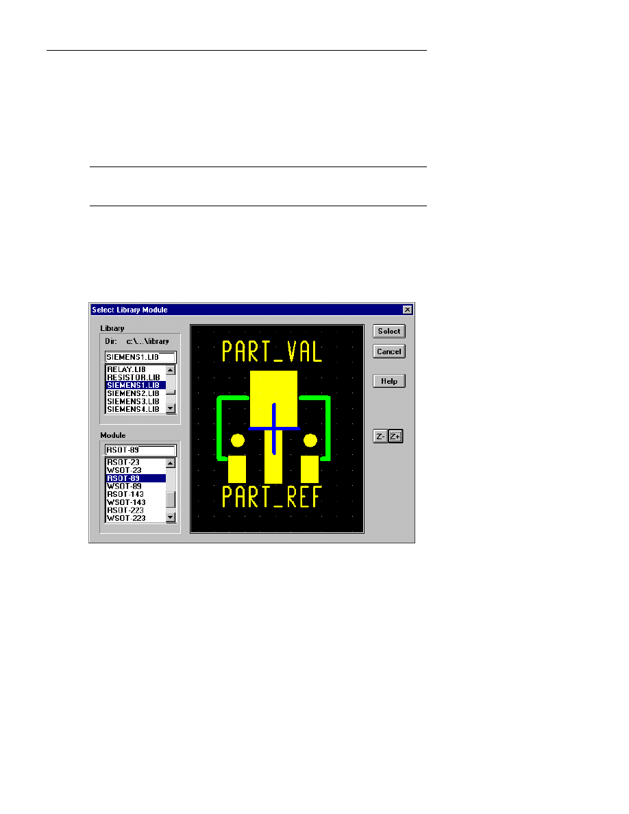
Use Libraries to view modules before adding them to the netlist. You can
view a particular module from the Module Libraries list box by double
clicking on the name of the module you want to view. Or you can click once
on the Libraries button. The Select Library Module dialog box displays as
shown next :
Figure 2-5.. The Select Library Module dialog box.

&KDSWHU0HQX5HIHUHQFH
31
Use the list boxes in the Select Library Module dialog box to select the
library and module you want to view. To copy the module name and library
name of a particular module into the Netlist Part Information list box, click
Select. To leave the Select Library Module dialog box without copying
anything, click Cancel.
Use Module Stuff List Load File to load a
.STF
file into the Module Stuff
List box. When you click on Load File, the Open File dialog box displays.
Select the file name you want loaded and click OK. WinBoard loads the
specified
.STF
file into the Module Stuff List box.
Use Module Stuff List Add Item to add the current Part Value, Module
Name, and Library Name from the Netlist Edit box to the Module Stuff List
box.
Use Module Stuff List Delete Item to remove the current line from the
Module Stuff List box.
Use Show First un/re-assigned to highlight and display the first part in the
Netlist Part Information list box that is either unassigned or has invalid
module information.
Use OK to tell the netlist loader to finish loading the netlist. The netlist
loader places the modules on the board file, writes out a stuff file with the
.STF
file extension, and updates the original netlist.
If your netlist was created with a netlist creation package for which
WinBoard supports automatic stuff back, the information from the
.STF
file
is also stuffed back into the schematic.
Anytime the netlist loader needs to overwrite a current file, you are asked if
the netlister should overwrite the already existing file.
Use Cancel to exit out of the netlist loading process. To protect your work
from being lost, a dialog box displays to make sure that you really want to
stop loading the netlist.
Use Help to display online help. The Help tool works similarly to online help
in other Windows-based applications.
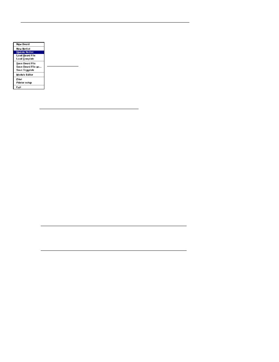
:LQ%RDUG/D\RXW5HIHUHQFH*XLGH
32
Update Netlist
Update Netlist is used to change modules or connections on a board using an
updated netlist file.
The Philosophy:
For proper documentation, it is suggested that changes are done on the
schematics. A board is not a documentation of a product -- it is the output.
Therefore, we suggest that changes should be made on the schematic and then
used to update the board file. This process is often referred to as Forward
Annotation.
Update Netlist may be used for the following items:
•
Delete parts (no longer used) on the schematic.
•
Add parts (new ) to the schematic.
•
Delete nets or connections.
•
Add nets or connections.
•
Change References.
•
Change Part Value.
•
Change Modules.
How Update Netlist works:
Each part placed on the schematic is assigned a unique identification called a
Time Stamp. A Time Stamp is added automatically by the schematic
program such as WinDraft. This Time Stamp is used to identify changes
between the existing board and the updated schematic (using the updated
netlist).
F
NOTE: If you are not using WinDraft (or a schematic program that
generates a time stamp) we suggest that you run an Annotation program to
check for duplicate references. The program can use the Reference
Designator for many of the functions instead of the Time Stamp.
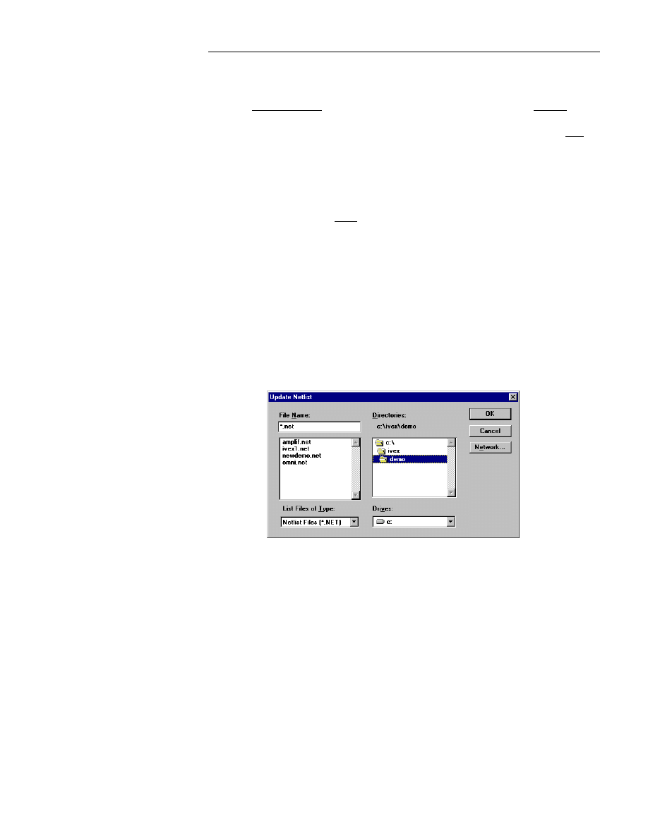
&KDSWHU0HQX5HIHUHQFH
33
Example 1: Delete a part.
If a part is deleted on the schematic, the time stamp associated with that part
no longer exists. Therefore, when you update the netlist it will remove the
module associated with that time stamp. This will occur even if a new part
was added to the schematic to replace the deleted one because it has a new
time stamp.
Example 2: Change the part value.
Edit the part value in the schematic without deleting or replacing the part.
This will keep the same time stamp. Therefore, when you update the netlist
the program will recognize the new part value for the time stamp and change
the board without deleting the module.
The Process
Follow these steps to use Update Netlist:
1.
Make the changes on the schematic and generate a new netlist.
2.
Load the board file.
3.
Select File from the menu, then select Update Netlist.
4.
Select the new netlist in the file seletion dialog box, then click OK.
Figure 2-6. :The Update Netlist dialog box.
5.
Choose the netlist format in the Convert Net File dialog box.
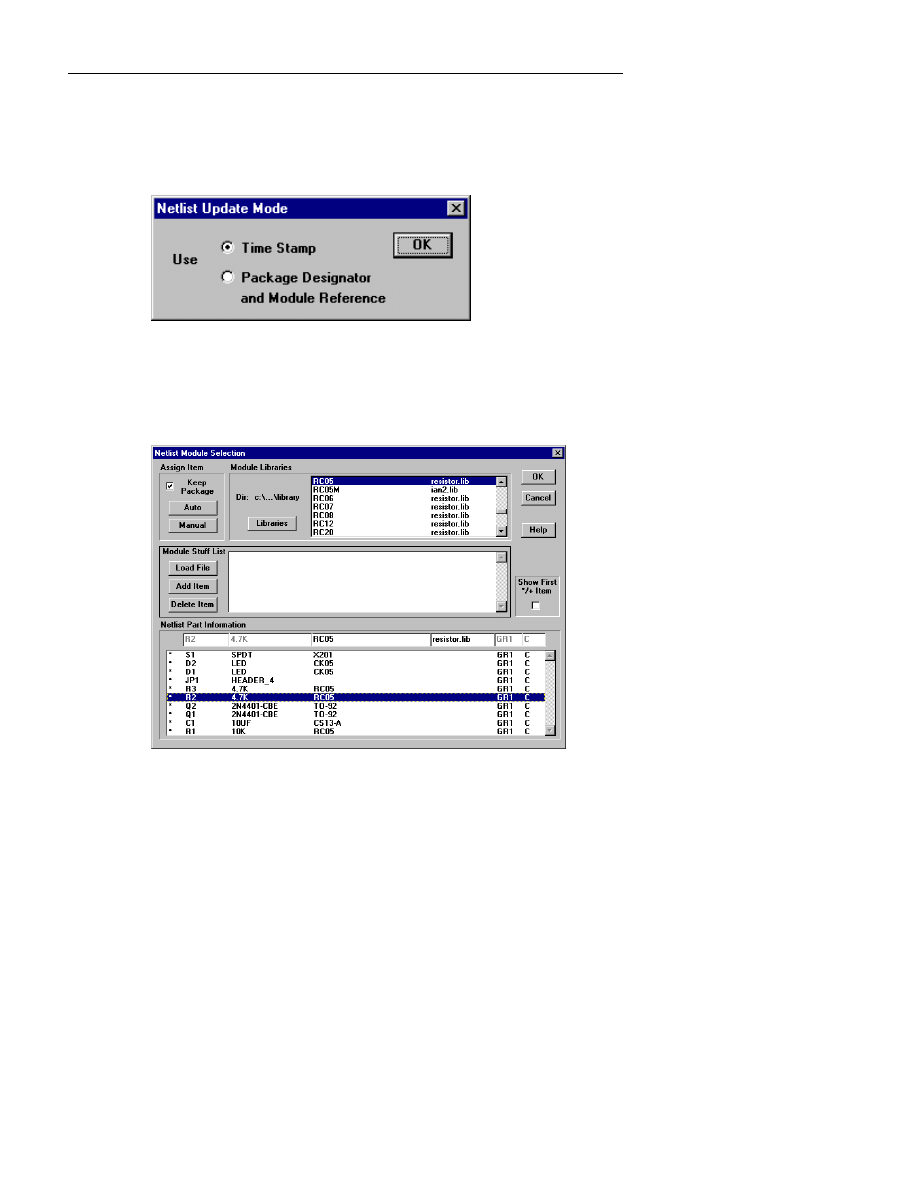
:LQ%RDUG/D\RXW5HIHUHQFH*XLGH
34
6.
Select the update mode in the Netlist Update Mode dialog box. The
choices are Time Stamp and Package Designator. Click Package
Designator if you want to use the modules Reference Designator. We
recommend that you only use the Time Stamp on an Ivex or WinBoard
netlist. Press OK.
Figure 2-7. : Netlist Update Mode
7.
The Netlist Module Selection dialog box opens. Verify the module
selection and library used in this dialog box before proceding. Make
sure that each part has a module footprint assigned. If no footprint is
assigned, an asterisk “*” will appear next to the item.
Figure 2-8. : The Netlist Module Selection dialog box
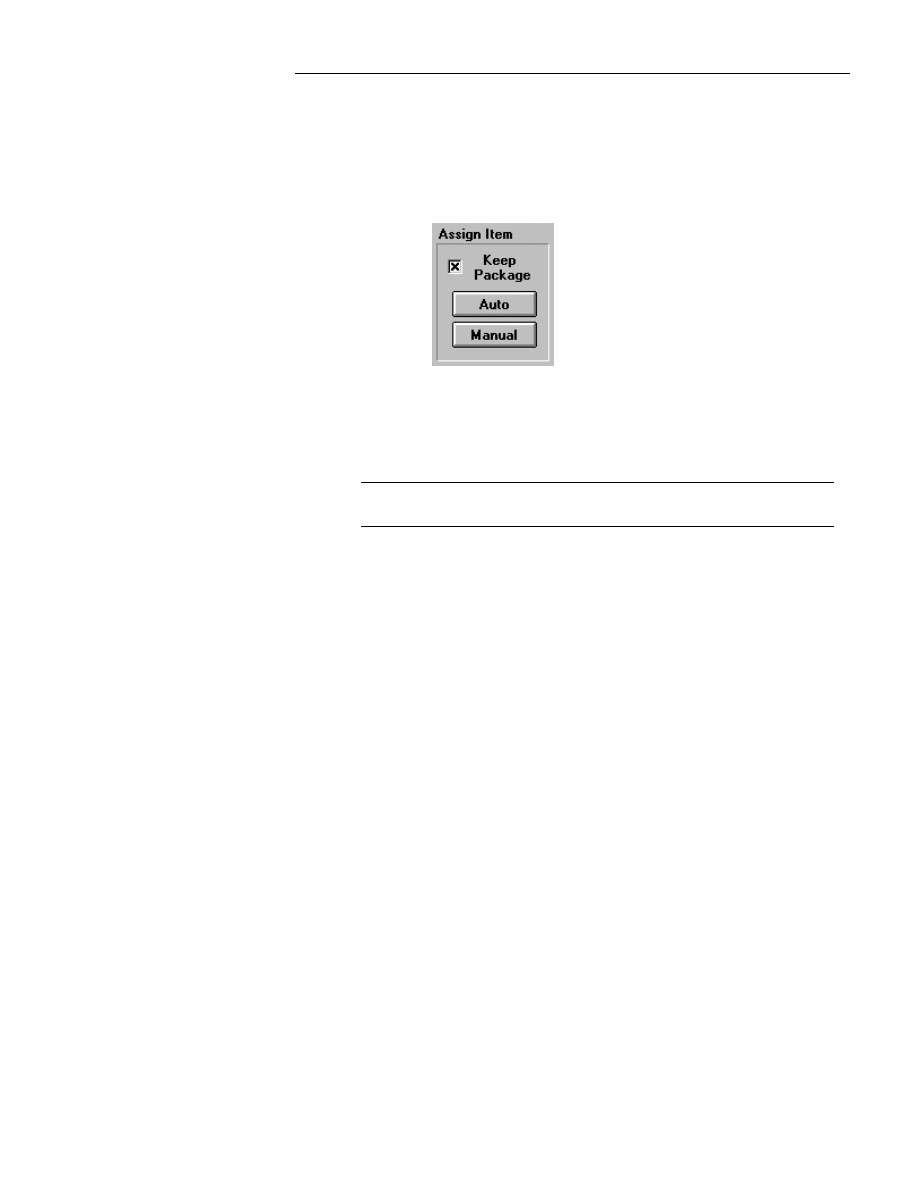
&KDSWHU0HQX5HIHUHQFH
35
An option in the Netlist Module Selection dialog box to Keep Package is
available. Check the box to use the package (module footprint) assigned in
the schematic netlist when using the Auto button. Remove the check from
the box and the Auto button will automatically replace the package with the
new selection to all parts with the same part value.
Press OK when all module footprints are correctly assigned to load or update
the netlist. The program loads the netlist and then updates the board
according to the changes made in the schematic.
F
NOTE: Refer to the load netlist section for detailed instructions on using
this function.
Summary of Changes with Update Netlist and their results:
Change made:
Result:
Deleted parts:
These are removed from the board.
Deleted parts with
tracks:
The module and the tracks associated with the
deleted module are removed from the board.
New parts:
These are placed outside the board outline.
Changed Part Ref and
Part Value
These values are updated on the board using the
existing module.
Printing and Plotting
WinBoard uses the standard printer and plotter drivers available for
Windows. Unless you specify otherwise, WinBoard prints to the Windows
default printer.
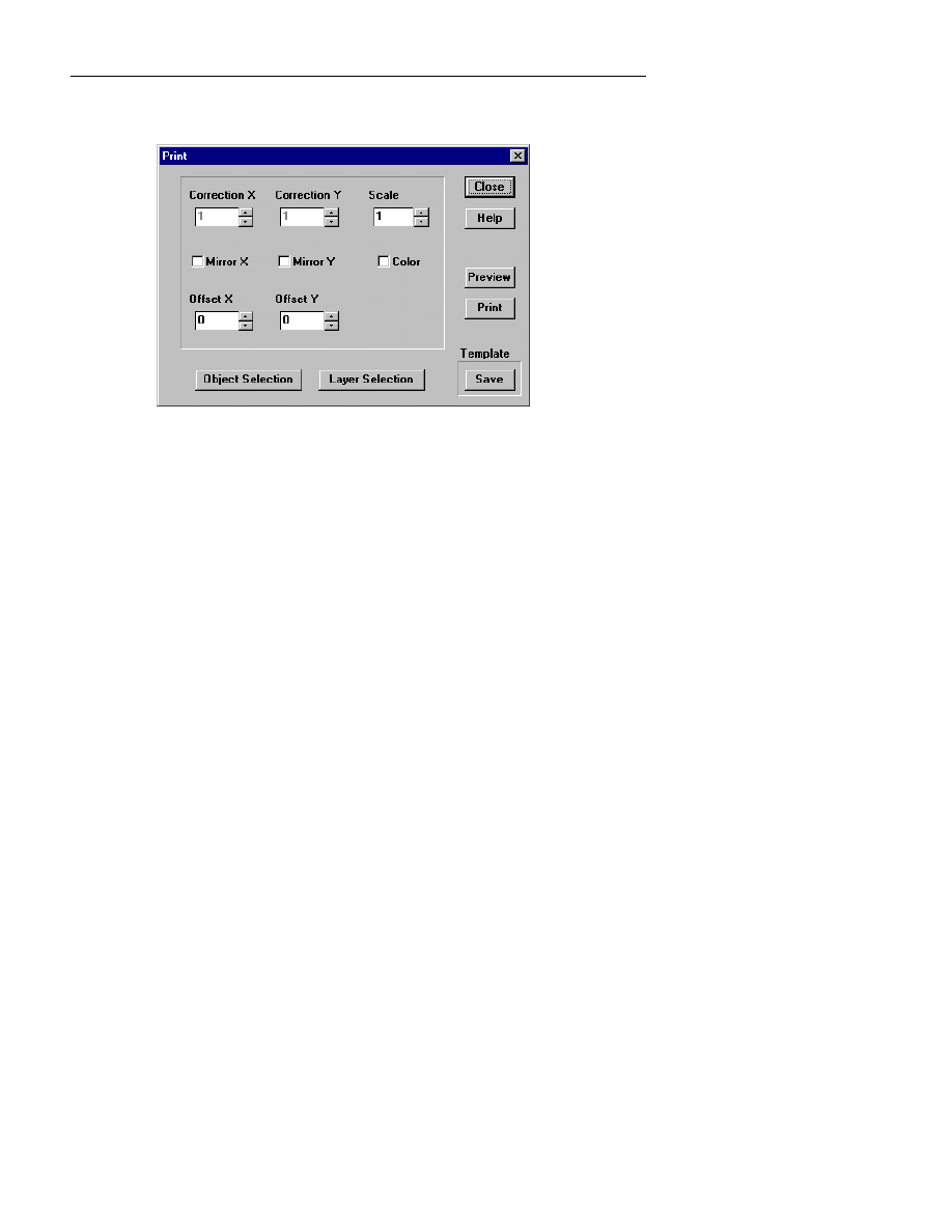
:LQ%RDUG/D\RXW5HIHUHQFH*XLGH
36
When you select Print from the File menu, a Print dialog box displays as
shown below.
Figure 2-9.. The Print dialog box.
Use Correction X to adjust the aspect ratio in the X direction. Enter a
number between 0.001 and 2.000. The default is 1 for a one to one aspect
ratio. Generally, these are only used to correct older dot matrix printers that
tend to distort the aspect ratio.
Use Correction Y to adjust the aspect ratio in the Y direction. Enter a
number between 0.001 and 2.000. The default is 1 for a one to one aspect
ratio. Generally, these are only used to correct older dot matrix printers that
tend to distort the aspect ratio.
Use Scale to specify the scale you want the board file printed or plotted in.
Any scale between 0.1 and 10.0 is acceptable. WinBoard’s printing and
plotting default scale is 1.0.
Use Mirror X to mirror the board in the horizontal axis. Check Mirror X to
mirror the board in the horizontal axis.
Use Mirror Y to mirror the board in the vertical axis. Check Mirror Y to
mirror the board in the vertical axis.
Use Offset X to specify the number of millimeters or inches—depending on
the units you have WinBoard set to in the Tools | Options dialog box—you
would like to offset the plot in the horizontal axis. A positive decimal number
from 0.1 to 16.0 is acceptable. The WinBoard default is zero.

&KDSWHU0HQX5HIHUHQFH
37
Use Offset Y to specify the number of millimeters or inches—depending on
the units you have WinBoard set to in the Tools | Options dialog box—you
would like the plot offset in the vertical axis. A positive decimal number from
0.1 to 16.0 is acceptable. The WinBoard default is zero.
Use Color to print in color if you are using a color printer. Preview will also
display the plot or print in color if this box is checked.
Use Preview to view the board before printing. This is very useful if you
make adjustments to the scale. You may need to adjust the X or Y offset to fit
the board on the paper, or change the paper orientation to landscape. For
more information about changing the paper orientation, use the File | Printer
Setup.
Use Close to exit the Print dialog box without printing or plotting anything.
Use Help to display online help. The Help tool works similarly to online help
in other Windows-based applications.
Use Print to accept any changes to the Print dialog box and print the board.
Use Template Save to save settings that you want to save for future use.
Use Object Selection to select the objects on each layer to be printed. For
more information about how Object Selection works, refer to Object
Selection below.
Use Layer Selection to select the objects on each layer to be printed. For
more information about how Layer Selection works, refer to Layer Selection
below.
Object Selection
The Object Selection dialog box is shown below. The Object Selection
dialog box is used for selecting what to print. For information about photo
plotting, refer to the CAM menu explanation later in this chapter.
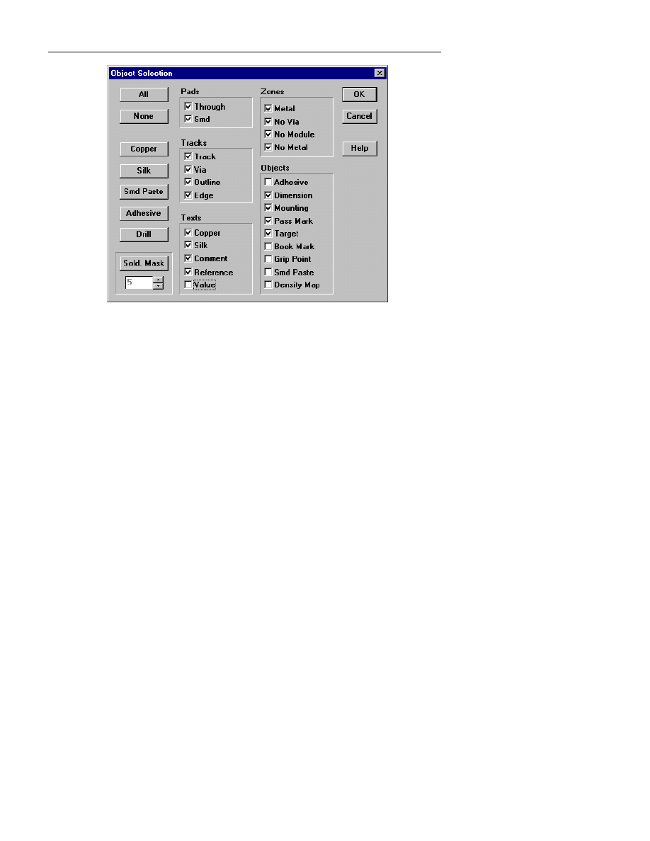
:LQ%RDUG/D\RXW5HIHUHQFH*XLGH
38
Figure 2-10.: The Object Selection dialog box.
Use All to select all objects—pads, tracks, text, zones, and objects—to print.
Use None to prevent any objects—pads, tracks, text, zones, and objects—
from printing.
Check any of the Pads items listed below that you want to have printed or
plotted:
Through
Prints through hole pads.
SMD
Prints SMD pads.
Check any of the Tracks items listed below that you want to have printed or
plotted:
Track
Prints all standard tracks on the layer.
Via
Prints any via on the layer—including through,
buried, and blind vias that end on or pass through
the layer.
Outline
Prints outlines for modules on the silk screen layer.
Edge
Prints the board edge. Edge is mostly used for
generating Cut Out Data for NC Drill machines, or
for documentation purposes.

&KDSWHU0HQX5HIHUHQFH
39
Check any of the Text items listed below that you want to have printed or
plotted:
Copper
Print copper text. Copper text may be selected on
all copper layers.
Silk
Print the silk screen text.
Comment
Print comment text. This is used for documentation
purposes.
Reference
Print module reference text.
Value
Print module value text.
Check any of the Zones items listed below that you want to have printed or
plotted:
Metal
Print Metal zones.
No Metal
Print No Metal zones.
No Via
Print No Via zones.
No Module
Print No Module zones.
Check any of the Objects items listed below that you want to have printed or
plotted:
Adhesive
Print adhesives.
Dimension
Print dimensioning.
Mounting
Print mounting holes.
Pass Mark
Print pass marks. Pass marks are mostly used on
multi-layer boards to identify the layer.
Target
Print targets. These are normally printed or plotted
on every layer
Book Mark
Print book marks.
Grip Point
Print the grip point.
Smd Paste
Print smd paste.
Density Map
Prints density map and histogram if visible
Use OK, after you have selected the objects to print or plot, to return to the
Print dialog box.

:LQ%RDUG/D\RXW5HIHUHQFH*XLGH
40
Use Cancel to exit the Object Selection dialog box without saving any
changes and display the Print dialog box.
Use Help to display online help. The Help tool works similarly to online help
in other Windows-based applications.
Other options include the following:
Selected Layer
Contents of the Selected Layer
Copper
The copper on any selected layer.
Silk
The silk screen for either side of the board file.
Smd Paste
The paste locations for SMD pads for the selected
layer.
Adhesive
The glue mark for SMD components
Drill
A drill drawing with separate symbols for each drill
hole size on the board.
Sold. Mask
The solder mask for either side of the board file.
Click on the Sold. Mask button and then type in the
value in the box below the button. For example :
select Sold. Mask and enter the value 6, this will
place a 6 mil solder mask around each pad.
Layer Selection
The Layer Selection dialog box is shown in the next figure. The Layer
Selection dialog box is used for selecting the layers to print or plot.
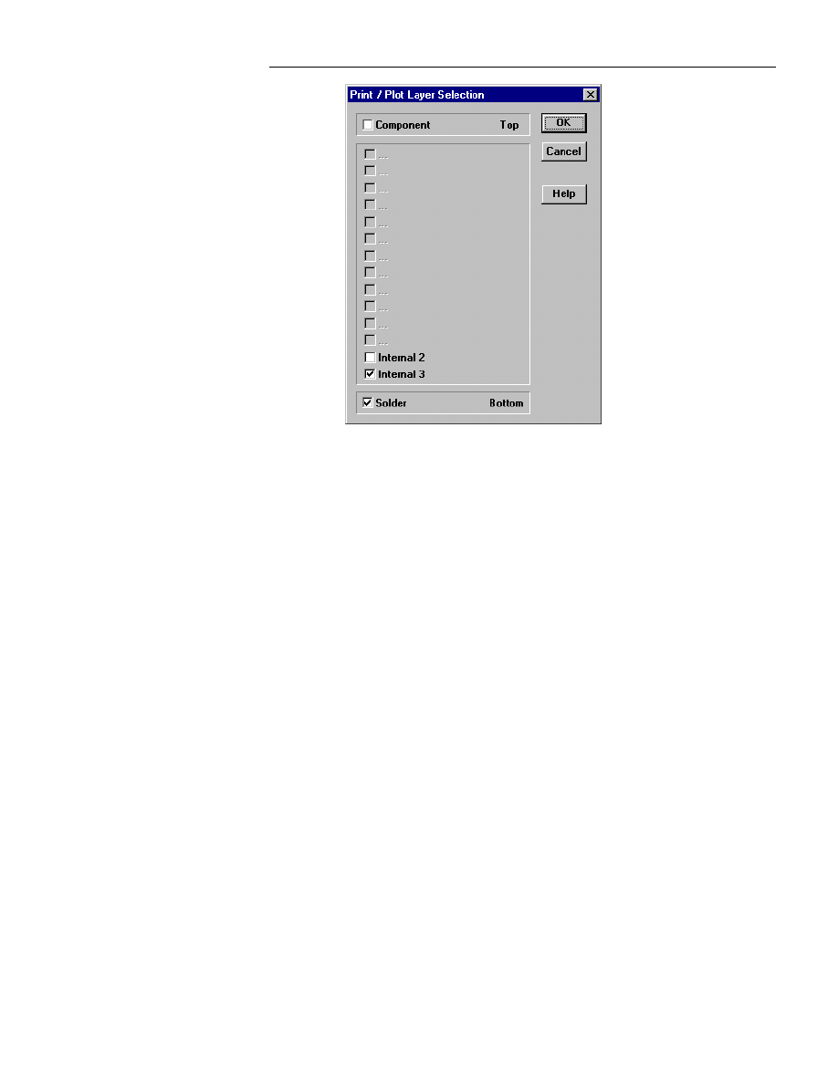
&KDSWHU0HQX5HIHUHQFH
41
Figure 2-11.. The Layer Selection dialog box.
Put a check next to the layer or layers you want to print or plot. The boxes
between Component and Solder are for selecting internal layers. The
internal layer selection check boxes are blank if the corresponding layer does
not exist. WinBoard does NOT allow an X to be placed in a check box for a
non-existing layer.
Use OK, after you have selected the objects to print or plot, to return to the
Print dialog box.
Use Cancel to exit the Print Layer Selection dialog box without saving any
changes and display the Print dialog box.
Use Help to display online help. The Help tool works similarly to online help
in other Windows-based applications.

:LQ%RDUG/D\RXW5HIHUHQFH*XLGH
42
Edit
Edit contains the menu selections in the Edit pull-down menu at left.
To cut or copy an object, select the object and click with the left mouse
button on Cut or Copy. You may also use the Windows shortcut keys
Ctrl+X
,
Ctrl+C, and Ctrl+V
.
Selecting Objects
Objects can be selected 3 ways:
1.
By clicking on the object with the left mouse button.
2.
By surrounding an object or a group of objects with a block.
3.
By clicking an object while holding down the Ctrl key. This enables you
to select more than one object at a time.
F
NOTE: Clicking again on another object or on no object unselects all
selected objects.
To paste an object that has already been copied to the clipboard:
1.
First, unselect the object copied to the clipboard by clicking on a blank
area.
2.
Click with the left mouse button on Paste in the menu. The object
displays on the screen and is still selected.
3.
To drag the pasted object to the correct location, press the left mouse
button and hold it while dragging the pointer to the appropriate location.
4.
Release the mouse button.
&KDSWHU0HQX5HIHUHQFH
43
F
NOTE: You may also use the standard Windows commands: Ctrl+X to Cut,
Ctrl+C to Copy and Ctrl+V to Paste..
Block Cut
Use Block Cut (or Ctrl+X) to copy all objects within a selected block to the
clipboard and delete them from the WinBoard file. Objects in the clipboard
can be pasted into any WinBoard file.
The Block Cut button remains dimmed and inactive until you select a block
of objects. For information about selecting a block of objects, see Selecting
Objects in Chapter 1: Editing Features.
Block Copy
Use Block Copy (or Ctrl+C) to copy all objects within a selected block to the
clipboard. Objects in the clipboard can be pasted into any WinBoard file.
The Block Copy button remains dimmed and inactive until you select a block
of objects. For information about selecting a block of objects, see Selecting
Objects in Chapter 1: Editing Features.
Block Paste
Use Block Paste to paste objects from the clipboard into a WinBoard file.
After you have cut or copied a block of objects to the clipboard, unselect the
objects by clicking with the left mouse button on a blank area. Follow these
steps to paste the block of objects into a WinBoard file:
1.
Click with the left mouse button on the Block Paste (or Ctrl+V) button.
The block of objects is copied from the clipboard into the WinBoard file
and remains selected.
:LQ%RDUG/D\RXW5HIHUHQFH*XLGH
44
2.
Move the pointer near the selected block of objects until the pointer
becomes a hand pointing at the block.
3.
Press and hold the left mouse button while dragging the selected block of
objects to its new location.
4.
When the block of objects is where you want it, release the left mouse
button. The block of objects is no longer selected after you release the
left mouse button.
CAUTION:
Be aware that it is possible to paste modules into your board
file that do NOT exist on your schematic. You can also paste modules with
identical part references to those already in your board file.
Delete
Delete removes the selected object, you may also use the Delete key on the
keyboard.
Select All
a
Select All (or Ctrl+A) may be used to select all objects on the board.
Find, Get & Place Module
Use Find, Get & Place Module to locate modules by reference name and
component type and to place a module using exact X, Y coordinates.
The Type and Autoplace Freeze areas in the Find, Get & Place Module
dialog box are reserved for future use. These functions are not currently
available.
The Find, Get & Place Module dialog box is shown below :
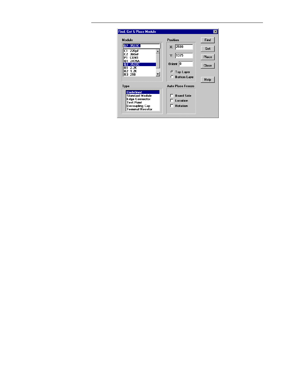
&KDSWHU0HQX5HIHUHQFH
45
Figure 2-12.. Find, Get & Place Module dialog box.
Use Find to locate a module. Follow these steps:
1.
Click with the left mouse button on a module name in the Modules list
box.
2.
Click with the left mouse button on Find. WinBoard returns to the main
WinBoard screen and pans the screen to the location of the module you
selected with the pointer pointing at anchor point of the module.
Use Get to select a module. Follow these steps:
1.
Click with the left mouse button on a module name in the Modules list
box.
2.
Click with the left mouse button on Get. WinBoard returns to the main
WinBoard screen, without changing the area of the board layout being
viewed, and the module you selected displays with the pointing hand,
indicating placement mode.
3.
Place the module in its new location.
Click on any module listed in the Module list and its coordinates are
displayed in the Position section of the dialog box as follows :
X: and Y: Displays the X and Y corrdinates in the appropriate boxes.
Orient: Displays the Orientation in one hundredth degree (.01) accuracy.
:LQ%RDUG/D\RXW5HIHUHQFH*XLGH
46
The radio buttons display Top Layer or Bottom Layer.
Use Place to place a module using the x, y coordinates as follows :
1.
Select the desired module in the Module section.
2.
Enter the Coordinates for the module in the Position section of the dialog
box. Enter X, Y coordinates, Orientation, and select the layer.
3.
Press the Place button to place the module at the new location.
Use Cancel to exit out of the Find & Get dialog box without saving any
settings.
Use Help to display online help. The Help tool works similarly to online help
in other Windows-based applications.
Global Edit
Use Global Edit to edit the parameters of all objects that are selected.
F
NOTE: You must first select the objects you want to edit before using
Global Edit, except for the delete zone feature.
CAUTION
: Every object you select is available for editing with the
Global Edit tool. Before you use Global Edit, make sure only the objects
you want to change are selected.
After you select the objects you want to edit, click on the Global Edit tool
button, or press
F3
. The Global Edit dialog box displays as shown next :
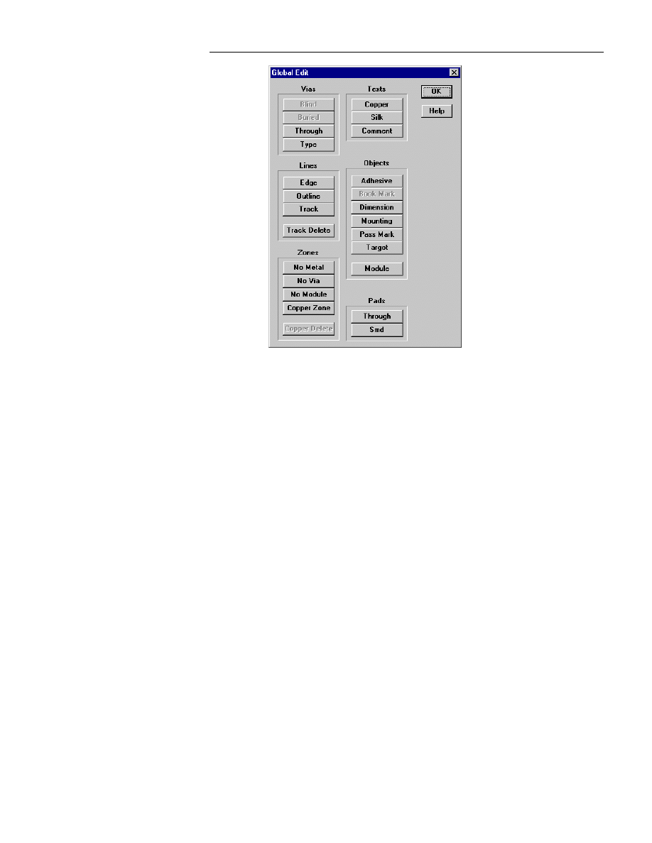
&KDSWHU0HQX5HIHUHQFH
47
Figure 2-13.. The Global Edit dialog box.
Notice in figure 2-13 that only some of the button names have bolded names.
The buttons with the bolded names are the objects available for editing.
Use the Vias buttons to change the parameters for the selected blind, buried,
and through pads. Type changes the vias from one via type to the via type
you select.
When you click the Blind, Buried, or Through button, the Edit Track
dialog box displays. Change the parameters as needed, and click OK.
Use the Zones buttons to change the parameters for the selected zones. When
you click any of the buttons in the Zones box, the Zone dialog box displays.
For more information about the Zone dialog box, refer to Chapter 2.
:LQ%RDUG/D\RXW5HIHUHQFH*XLGH
48
Press the Copper Delete button to remove all copper zones on the board. Do
not select the zone to use this function. This is the only Global Edit
command that does not require selecting the objects first.
Use the Lines buttons to change the parameters for the selected edges,
outlines, and tracks. When you click Edge, Outline, or Track, the Edit
Track dialog box displays. Change the parameters as needed, and click OK.
Press the Track Delete button to delete all selected tracks. A confirmation
box appears in which you must select Yes or No.
Use the Texts buttons to change the height, width, thickness, spacing, or
slant of the selected copper, silk screen, and comment text. When you click
any of the buttons in the Text box, the Text dialog box displays.
Use the Pads buttons to edit the pad stack for the selected objects. When you
select Through or Smd, the Pad Stack dialog box displays. For more
information about changing the parameters in the Pad Stack dialog box, refer
to Editing Pad Stacks in Chapter 1: Editing Features.
CAUTION
: Be careful when editing pad stacks. If you edit a pad stack and
click OK, all of the pads with the same pad stack name as the pad stack you
edited are changed. This includes all pads on the board with that pad stack
name, NOT merely the selected pads.
If you want to change the selected pads only: in the Pad Stack dialog box,
enter a new name in the Board Pad Stack List and use New. For more
information about how to change pad stack characteristics, refer to Editing
Pad Stacks in Chapter 1: Editing Features.
Use the Objects buttons to change the parameters for the selected Adhesive
objects, book marks, dimensions, mounting holes, pass marks, and targets.
When you click any of the buttons in the Objects box, the dialog box for that
object displays.
For more information about each of the dialog boxes, refer to the particular
object by tool name in Chapter 2.
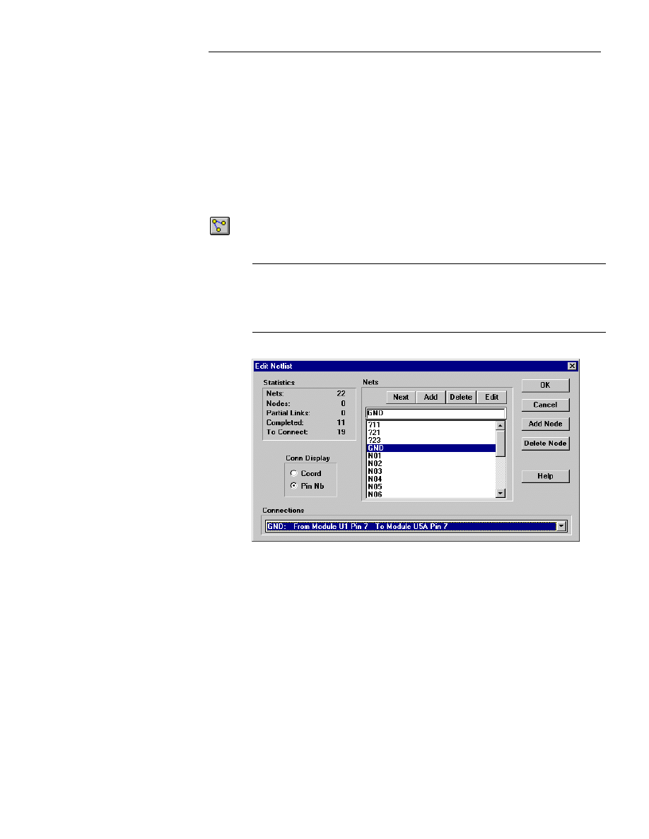
&KDSWHU0HQX5HIHUHQFH
49
Use the Module button to replace an existing module on the board. It will
only replace modules with the exact same number of pins. Be very careful,
the replacement module must be an exact match.
Use Help to display online help. The Help tool works similarly to online help
in other Windows-based applications.
Edit Netlist (Netlist On the Fly)
Use Edit Netlist (also called Netlist On the Fly) to edit an existing netlist or to
create a complete netlist.
F
NOTE: Since most designs need schematic documentation attached to them,
we recommend you start with a schematic. Building a printed circuit board
before creating the schematic is sort of like drawing the blueprints for a
house after the house has been built.
The Edit Netlist dialog box is shown below :
Figure 2-14.. The Edit Netlist dialog box.
Use Add Node to add connections to a net. Follow these steps:
1.
Type a name in the Nets list box—or click on a name that is already
listed.

:LQ%RDUG/D\RXW5HIHUHQFH*XLGH
50
2.
Click with the left mouse button on Add Node. The Main WinBoard
screen displays and the pointer changes to look like this:
signifying
the net connection mode. While WinBoard is in net connection mode,
you can toggle between Add Node and Delete Node by pressing
x
. The
delete node pointer looks like this:
.
3.
Click with the left mouse button on all pads you want to become part of
the same net.
F
NOTE: If you decide you would rather not add connections to the net after
all, press
Esc
or click the right mouse button to return to the normal mode.
Use Delete Node to disassociate a net from a particular pad. Follow these
steps:
1.
Click with the left mouse button in the Nets list box on the net name
associated with the pad from which you want to remove the connection.
2.
Click on Delete Node. The Main WinBoard screen displays and the
pointer changes to look like this:
signifying the delete node mode.
While WinBoard is in delete node mode, you can toggle between Delete
Node and Add Node by pressing
x
. The add node pointer looks like this:
.
3.
Click on any pad you want removed from the net. The net name for the
pad you clicked on is set to zero and the ratsnest disappears from that
pad.
Use Nets Next to increase by one the net that is highlighted in the list box.
For example, if the net name in the Nets list box is
NET
, clicking on Next
would cause WinBoard to add a net named
NET1
to the nets.
Use Nets Add to add the net name from the Nets list box to the board.
Use Nets Delete to delete the selected net name from the Nets list box and
remove all connections on the board that belonged to that net.
Use Nets Edit to change an existing net name. Simply select a net name from
the Nets list box and click on Edit. The netname is changed on all pads
associated with the selected net.
Use Connections to display all the net connections on the board file.
Use Coord to set the way the net connections are displayed in the
Connections list box to X, Y coordinates.

&KDSWHU0HQX5HIHUHQFH
51
Use Pin Nb to set the way the net connections are displayed in the
Connections list box to pin numbers with module names.
Use Cancel to exit out of the Edit Netlist dialog box without saving any
settings.
Use Help to display online help. The Help tool works similarly to online help
in other Windows-based applications.
F
NOTE: To display the status of a pin, trace or zone, place the pointer over
the object and press the F2 key on the keyboard. This will display the pin
and net name in the Windows status area (lower left corner of the screen).
Adding a Connection
To add a node to a net, also known as adding an existing net to an open pad
on an existing module, follow these steps:
1.
Click on the Edit Netlist button. The Edit Netlist dialog box displays.
2.
Click on the net in the Nets list box to which you want to connect the
pad.
3.
Click on Add Node. The main WinBoard screen displays and the pointer
looks like this:
, signifying the Add Node mode. The yellow ratsnest
is the net to which you want to connect the pad. The ratsnests for all
other nets are gray.
4.
Click with the left mouse button on the pad to be added to the net—or
use the
b
key.
If the pad was not connected to a net, the connection will simply be made. If,
however, the pad was already a part of a different net, WinBoard will ask
you if you want to overwrite the existing net name.
5.
Continue clicking on pads that you want added to the net.
6.
To leave the add net mode and save your changes, press
Esc
or click the
right mouse button.
You can toggle between the add node mode and the delete node mode simply
by pressing the
x
key.
Deleting a Connection
To delete an existing net connection from a pad, follow these steps:

:LQ%RDUG/D\RXW5HIHUHQFH*XLGH
52
1.
Click on the Edit Netlist button.
2.
From the Nets list box, select the net to which the pad you want to
remove from the net is connected.
3.
Click on the Delete Node button. The WinBoard main screen displays.
The yellow ratsnest shows the net you selected from which to delete a
node. All other nets have gray ratsnests. The pointer looks like this:
,
signifying the Delete Node mode.
When WinBoard is in delete node mode, and you click on a pad connected to
the highlighted net, the node is deleted from that net.
4.
Find the pad you need to disconnect from the net and click on it with the
left mouse button. The ratsnest disappears from the pad and the net name
changes to
NULL
. Each time you click on a pad connected to the yellow
net, that node is deleted from the net.
If you click on a pad which belongs to a different net, WinBoard tells you
that you cannot delete a node that is part of another net. Click on OK to
continue.
5.
To exit the delete node mode, either press
Esc
or click the right mouse
button.
If you delete the wrong pad from the net you can toggle to the Add Node
mode simply by pressing the
x
key, click on the pad to add the connection,
and return to the Delete Node mode by pressing the
x
key again.
Adding a New Net
To add a new net to the netlist, follow these steps:
1.
Click on the Edit Netlist button.
2.
Click in the Nets list box and type the name of the new net.
3.
Click on the Nets Add button. Even though there are no connections
connected to the net, the net is added to the netlist.
4.
Click on the Add Node button to add this new net to pads of a module
on the board file (see Adding a Connection). If you do not use the net,
WinBoard will prompt you to remove it.
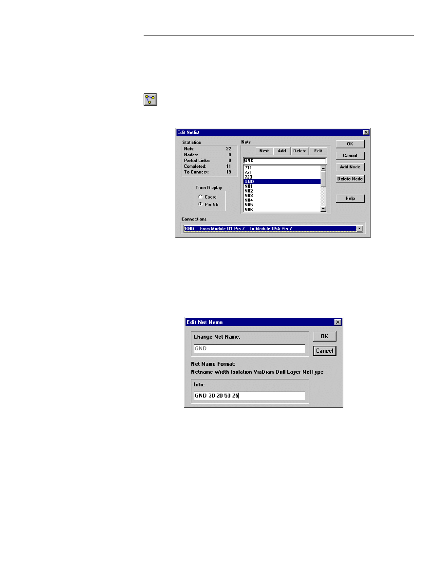
&KDSWHU0HQX5HIHUHQFH
53
Edit net characteristics
Net characteristics such as track width and isolation may be edited directly on
the board file using the Edit Netlist function.
Click on the icon at left to load the Edit Netlist dialog box and follow the
steps below to change the net characteristics:
Figure 2-15. : The Edit Netlist dialog box.
1.
Select the net to edit in the Edit Netlist dialog box, for example
GND.
2.
The Edit button is now highlighted above the selection. Press the
Edit button to make changes. This opens the following dialog box:
Figure 2-16. : The Edit Net Name dialog box.
:LQ%RDUG/D\RXW5HIHUHQFH*XLGH
54
3.
In the Edit Net Name dialog box, enter the changes in the lower text
box marked Into: Use the format as shown directly over the box as
follows:
Netname Width Isolation ViaDiam Drill Layer NetType
In the example above, the net named GND is changed so that the
width is 30, isolation is 20, via diameter is 50 and the drill hole is 25.
4.
Press OK to make the changes.
Undo
When the Undo button is active, you can undo commands by clicking once on
the Undo button. You can use Undo to: undelete objects and undo moves.
Undo will continue undoing as many as thirty-two consecutive commands.
View
View contains the menu selections shown in the View pull-down
menu at left.
Zoom in
Use Zoom in to zoom in to a smaller area of the board file. The
Home
and
End
keys on the keyboard may also be used to zoom in and out.
Follow the steps below to zoom in:
1.
Select the Zoom in button. The pointer changes to:
, signifying that
WinBoard has entered the zoom in mode. The view on the screen pans as
you move the pointer.
2.
Place the pointer in the center of the area to zoom in on and click the left
mouse button once.
&KDSWHU0HQX5HIHUHQFH
55
3.
To escape from autopan mode, click the right mouse button once.
Zooming is done in the same increments as those available for scaling the
WinBoard drawing.
Zoom out
Use Zoom out to zoom out to a larger area of the board file. The Home and
End keys on the keyboard may also be used to zoom in and out.
Follow the steps below to zoom out:
1.
Select the Zoom out button. The pointer changes to:
, signifying
that WinBoard has entered the zoom out mode. The view on the screen
pans as you move the pointer.
2.
Place the pointer in the center of the area from which to zoom out, and
click the left mouse button once.
3.
To escape from autopan mode, click the right mouse button once.
Zooming is done in the same increments as those available for scaling the
WinBoard drawing. The table below shows the available zoom and scale
increments:
Mils
Millimeters
µ
m
.5 mil
0.005 mm
.5
µ
m
1 mil
0.01 mm
1
µ
m
2 mils
0.02 mm
2
µ
m
5 mils
0.05 mm
5
µ
m
10 mils
0.1 mm
10
µ
m
20 mils
0.2 mm
20
µ
m
50 mils
0.5 mm
50
µ
m
100 mils
1 mm
100
µ
m
200
µ
m
500
µ
m
:LQ%RDUG/D\RXW5HIHUHQFH*XLGH
56
Zoom Best
Use Zoom Best to fit the current board file into the screen. When Zoom Best
fits the board to the screen, the zoom scale may be fractional and the grid dots
will probably not align. Nevertheless, whatever routing grid is selected will
have the exact spacing as specified, it is just the display that appears different.
After you press zoom best, the program will automatically toggle back to the
previous zoom scale when you zoom in (Home key) or zoom out (End key).
CAUTION:
If you notice that the board does not properly fit the screen, this
could be the result of a faulty module footprint. For example: if the board
gets really small, this is due to a module footprint that was created without a
reference marker, or if the reference marker was moved away from the
module before it was saved. The Reference marker determines the size and
rotation point for a module. If the reference marker is moved or deleted the
module will seem to be extremely large—thus the board seems to shrink when
performing zoom best. This problem should be corrected in the module
immediately before proceeding.
Zoom Refresh Screen
Use Refresh Screen to redraw the displayed area of the WinBoard drawing.
The
Z
key on the keyboard performs the same function.
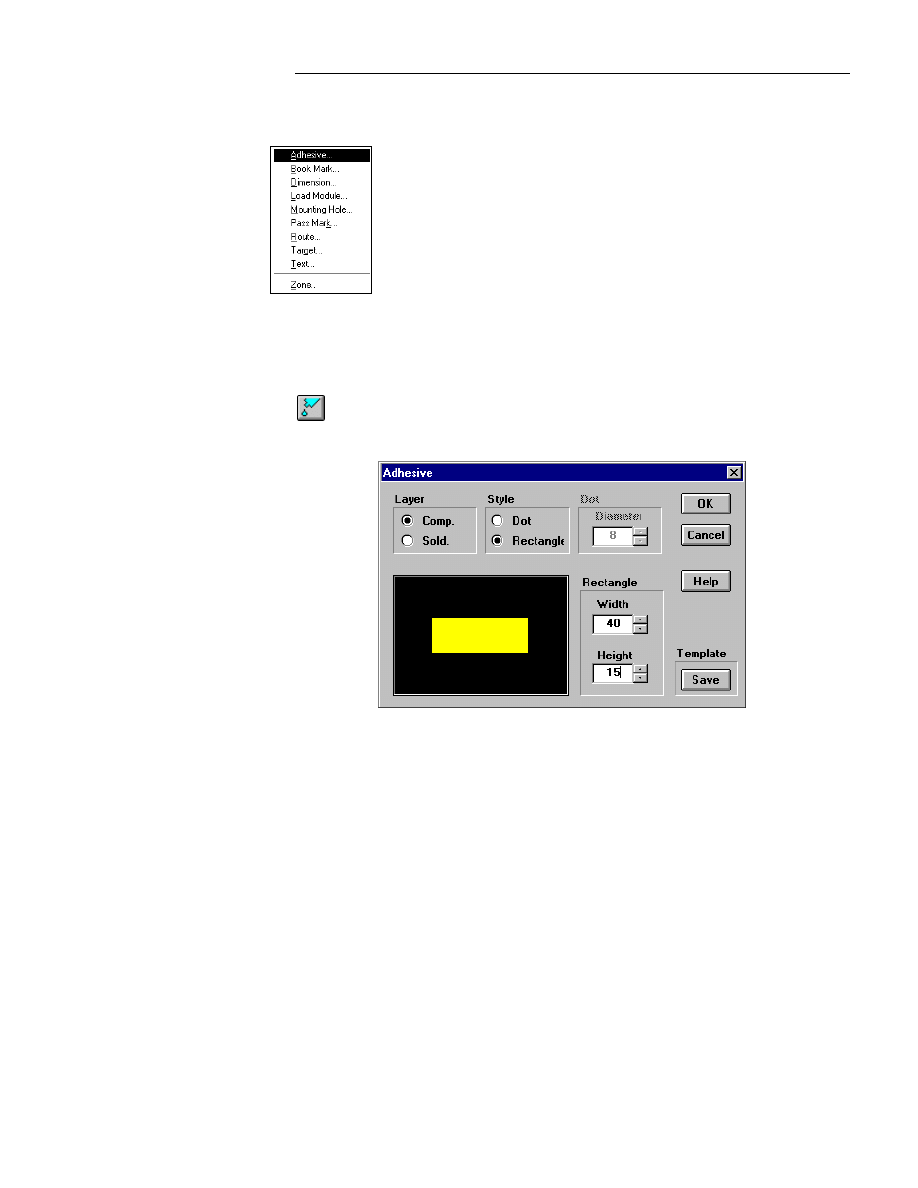
&KDSWHU0HQX5HIHUHQFH
57
Place
Place contains the menu selections shown in the Place pull-down
menu at left.
When you select an item on the Place pull-down menu, the dialog
box for the selected tool displays.
After you click OK in any dialog box, WinBoard enters autopan
mode. This means that the view on the screen pans as you move the
pointer. To escape from the Place mode, press
Esc
or click the right
mouse button once.
Adhesive
Use Adhesive to create adhesive dots to place on your board file. Adhesive
dots are used for attaching SMDs to the PC board in manufacturing.
The Adhesive dialog box is shown below :
Figure 2-17.. The Adhesive dialog box.
Use Style to select either a rectangular or circular adhesive dot.
Use Layer to select whether the adhesive dot is placed on the component or
solder layer of the PC board.
Use the Dot section of the Adhesive dialog box to set the diameter of a
circular adhesive dot.
:LQ%RDUG/D\RXW5HIHUHQFH*XLGH
58
Use the Rectangle section of the Adhesive dialog box to set the width and
height of the adhesive dot.
Use OK to accept the changes you have made to the Adhesive dialog box
and to re-display the main WinBoard dialog box.
Use Cancel to exit out of the Adhesive dialog box without saving any
settings.
Use Help to display online help. The Help tool works similarly to online help
in other Windows-based applications.
Use Template Save to save adhesive parameters that you want to save for
future use.
BookMark
Use BookMark to mark different places on the WinBoard board file that you
would like to be able to find easily. You place a book mark at a particular
location on the board file. Then, when you are editing at a different location
and want to move back to the location of the book mark, you use the book
mark button to pan the screen back to that location.
A valid bookmark name is an eight (8) digit alphanumeric character string
without spaces.
F
NOTE: You can have an unlimited number of book marks in any
WinBoard PC board file.
To display the BookMark dialog box from the main WinBoard screen,
simply double-click on any book mark.
The BookMark dialog box is shown below :
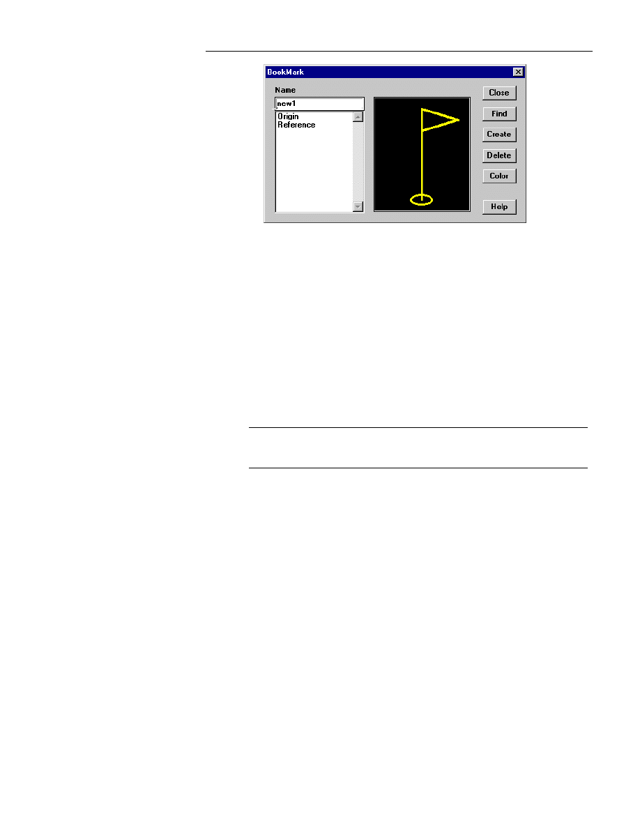
&KDSWHU0HQX5HIHUHQFH
59
Figure 2-18.. The BookMark dialog box.
Use Color to change the color of the book mark selected in the Name list
box. When you select a book mark from the Name list box and click Color,
the Color dialog box displays. Select a color or create a custom color and
click OK to change the selected book mark’s color.
The Origin BookMark
When you create a new board file, WinBoard automatically places a book
mark named Origin at coordinates (0,0). The Origin book mark defines the
origin of the coordinate display and of the board file, and can be dragged to
define a new origin. Changing the location of the Origin book mark makes it
possible to use negative coordinates to the left and above the Origin book
mark. There is only one Origin book mark per board file.
F
NOTE: The Origin book mark does not determine the film origin for CAM
reports. The Film Origin is always the upper left hand screen corner.
To move the Origin book mark, follow these steps:
1.
Select the Origin book mark by clicking on it with the left mouse button.
When you release the mouse button and move the pointer near the book
mark, the pointer becomes a pointing hand. It may also help to select
Origin in the bookmark dialog box and then press Find. This will place
your cursor at the point of the bookmark.

:LQ%RDUG/D\RXW5HIHUHQFH*XLGH
60
2.
Place the pointer at the bottom of the book mark flagpole then press and
hold down the left mouse button while dragging the book mark to its new
location.
3.
When the book mark is where you want it, release the mouse button.
Coordinates (0,0) move with the Origin book mark. When you move the
pointer to the left of the Origin book mark, the X coordinate has a
negative value. When you move the pointer above the Origin book mark,
the Y coordinate has a negative value.
F
L
NOTE: The Origin book mark cannot be deleted from the BookMark
dialog box.
Use the L key on the keyboard to reset the origin bookmark to the screen
origin.
Reference Book Mark
The Reference book mark is used as the rotation point for modules and it
determines the size of a module. It is usually placed at pin one on through
hole modules and at the center point on SMD modules. The Reference book
mark is required on each module, DO NOT DELETE IT.
The Reference Bookmark may also be used to move a group of objects using
exact X and Y coordinates. See Chapter 1: Editing Features, Move object to
exact X,Y Coordinates.
Creating and Placing a User Book Mark
To place a book mark, follow these steps:
1.
Click with the left mouse button on the BookMark button.
2.
Click in the text entry part of the Name list box and type the name you
want the new book mark to have. The name you type displays in the list
box below where you typed it.
3.
Select the color you want for the book mark by clicking on the Color
button and selecting the appropriate color from the Color dialog box.
4.
Click with the left mouse button on the Create button. The main
WinBoard screen displays and the pointer changes to:
with a
highlighted book mark attached, signifying that WinBoard has entered
book mark placement mode.
&KDSWHU0HQX5HIHUHQFH
61
5.
Place the pointer where you want the book mark and click the left mouse
button. The new book mark displays.
Finding a Book Mark
To find any previously placed book marks, follow these steps:
1.
Click with the left mouse button on the BookMark button.
2.
Click in the Name list box on the name of the book mark you want to
find. The name of the book mark displays in the text entry part of the
Name list box.
3.
Click with the left mouse button on the Find button. The main WinBoard
screen displays at the location of the book mark you selected in step two
above.
F
NOTE: DRC bookmarks are listed in the DRC menu.
Deleting a Book Mark
Use Delete to delete book marks one at a time. Highlight the name of the
book mark you want to delete from the list box by clicking on it with the left
mouse button. Then Click with the left mouse button on Delete.
You can also delete a book mark from a board file by simply clicking on it to
select it and pressing the
Del
key.
Dimensioning
Use Dimensioning to set the Internal or External Arrow Style, Arrow Height,
Arrow Length, and Arrow Thickness dimensioning parameters, and to place
dimensioning in the board file.
The Dimensioning dialog box is shown below :
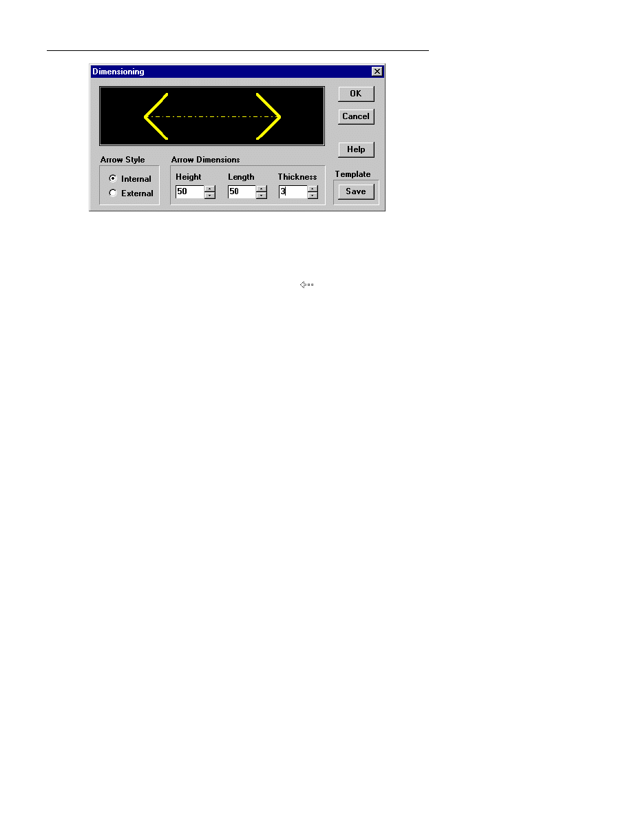
:LQ%RDUG/D\RXW5HIHUHQFH*XLGH
62
Figure 2-19.. The Dimensioning dialog box.
Use Template Save to save dimensioning parameters that you want to save
for future use.
Once the Dimensioning parameters have been set, click OK. The main
drawing screen displays, the pointer changes to:
, signifying that
WinBoard has entered the dimensioning mode. WinBoard simultaneously
enters autopan mode. This means that the view on the screen pans as you
move the pointer. To escape from autopan mode, press
Esc
or click the right
mouse button once.
Use Cancel to exit out of the Dimensioning dialog box without saving any
settings.
Use Help to display online help. The Help tool works similarly to online help
in other Windows-based applications.
Placing Dimensions
Follow the steps below to place dimensions:
1.
Select Place | Dimension. This opens the Dimensioning dialog box.
2.
Select Internal or External arrow style and press OK.
3.
Place the pointer at the location where you want the first point of the
dimensioning line.
4.
Click the left mouse button to begin (or press the B key to Begin).
5.
Move the pointer to the final point on the dimensioning line and click the
left mouse button.
To continue placing dimensioning arrows, repeat the steps above.
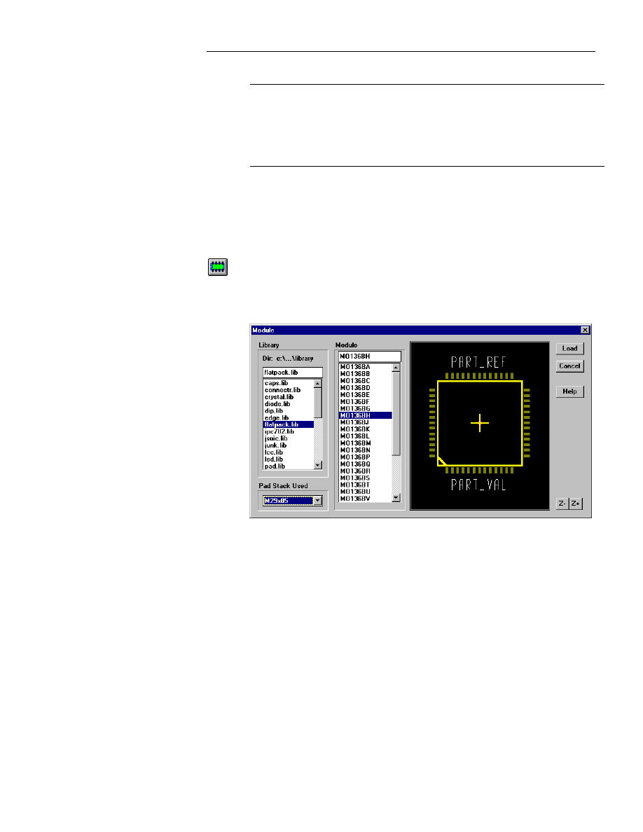
&KDSWHU0HQX5HIHUHQFH
63
To stop placing dimensions, press
Esc
.
F
NOTE: If you prefer, you may place by pressing the left mouse button or by
using the keyboard hotkeys. Select “Route with left mouse button” in the
Options dialog box. You can use the keyboard to select Begin, End, and
escape. Instead of clicking with the mouse button, press
b
for Begin,
n
for
End, or
Esc
for escape
.
If you start to place another dimension and then decide you don’t need
another one, just select Escape from the menu that displays or press
Esc
.
Module
Use Module to select the library directory and the modules to view or load,
and to place modules in the board file.
The Module dialog box is shown below :
Figure 2-20.. The Module dialog box.
Use Load to load a module into the board file.
Use Cancel to display the main WinBoard screen without loading a module.
Use Z+ and Z- to zoom the view of the module in and out.

:LQ%RDUG/D\RXW5HIHUHQFH*XLGH
64
Use Help to display online help. The Help tool works similarly to online help
in other Windows-based applications.
Viewing Modules
To view a module:
1.
Select the module library name in the Library Dir: list box.
2.
Select the module name from the Module list box. The module displays
in the view box.
3.
Use the Z+ and Z- buttons to zoom in on or zoom out from the view of
the module.
Loading and Placing Modules
To load a module in WinBoard, follow these steps:
1.
Select the module library name in the Library Dir: list box.
2.
Select the module name from the Module list box.
3.
Click with the left mouse button on the Load button. The main drawing
screen displays and the pointer changes and has a module outline
attached, signifying that WinBoard has entered placement mode.
4.
Place the pointer at the location where the module’s reference point
should be and click the left mouse button.
To place another module, click with the left mouse button on the Module
button again and select the appropriate module.
Loading a single pad module or testpoint
To place a module with only one pad, select the library pad.lib. Then select
the module named Pad1 and place it on the board. Notice that a single pad
module will still have module text (PART_REF and PART_VAL). The text
is required and it cannot be deleted, however it can be turned off so that it
does not display in the Tools | Options | Object Selection dialog box.
Double click on the pad to change the size or shape. This will open the Pad
Stack dialog box. Make the desired change such as rectangle to square, press
Edit and then Assign the new shape. For more information, refer to Editing
Pad Stacks.
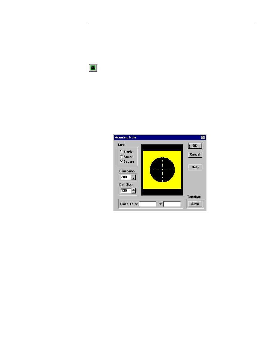
&KDSWHU0HQX5HIHUHQFH
65
To place a Test Point, use one of the pre-defined modules in the tstpoint.lib.
This library contains both through hole and SMT testpoint modules.
Mounting Hole
Use Mounting Hole to set the style, dimensions, and drill size of mounting
holes, and to place mounting holes in the board file. If you choose the Empty
style, the mounting hole has no copper and is just a drill hole.
Use Drill Size to select the size of the drill hole.
Use Dimension to select the width (annular ring) for the copper around a
Round or Square Mounting Hole.
Use Place At to enter the exact X and Y coordinates to place the mounting
hole.
The Mounting Hole dialog box is shown below :
Figure 2-21.. The Mounting Hole dialog box.
Use OK to accept the changes you have made to the Mounting Hole dialog
box and to re-display the main WinBoard dialog box.
Use Cancel to exit out of the Mounting Hole dialog box without saving any
settings.
Use Help to display online help. The Help tool works similarly to online help
in other Windows-based applications.

:LQ%RDUG/D\RXW5HIHUHQFH*XLGH
66
Use Template Save to save mounting hole parameters you want to save for
future use.
Placing Mounting Holes
Once you have set the Mounting Hole parameters, click OK. The main
drawing screen displays, the pointer changes to:
, and a mounting hole
outline appears, signifying that WinBoard has entered placement mode.
To place mounting holes follow these steps:
1.
Place the center of the mounting hole outline at the location where the
mounting hole should be.
2.
Click the left mouse button.
3.
To continue placing mounting holes, move the pointer to the next
location and click the left mouse button again.
To stop placing mounting holes, press
Esc
.
To place a different type of mounting hole, click with the left mouse button
on the Mounting Hole button again and change to the appropriate mounting
hole.
Pass Mark
Pass Marks are used to designate the number of layers on a printed circuit
board and to identify each layer.
Use Pass Mark to set the text and frame width, height, and thickness of pass
marks and to place pass marks in your board file.
The Pass Mark dialog box is shown below :
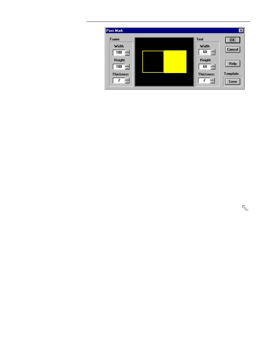
&KDSWHU0HQX5HIHUHQFH
67
Figure 2-22.. The Pass Mark dialog box.
Use Frame Width, Frame Height, and Frame Thickness to set the width,
height, and thickness of the pass mark frame.
Use Text Width, Text Height, and Text Thickness to set the width, height,
and thickness of the pass mark text.
Use OK to accept the changes you have made to the Pass Mark dialog box
and to re-display the main WinBoard dialog box.
Use Cancel to exit out of the Pass Mark dialog box without saving any
settings.
Use Help to display online help. The Help tool works similarly to online help
in other Windows-based applications.
Use Template Save to save pass mark parameters that you want to save for
future use.
Placing Pass Marks
To place pass marks after you have set the pass mark parameters:
1.
Click OK. The main drawing screen displays, the pointer changes to:
,
and a pass mark outline appears, signifying that WinBoard has entered
placement mode.
2.
Place the pass mark outline at the location where you want the pass
mark.
3.
Click the left mouse button.
4.
To continue placing the same type of pass mark, move the pointer to the
next location and click the left mouse button again.
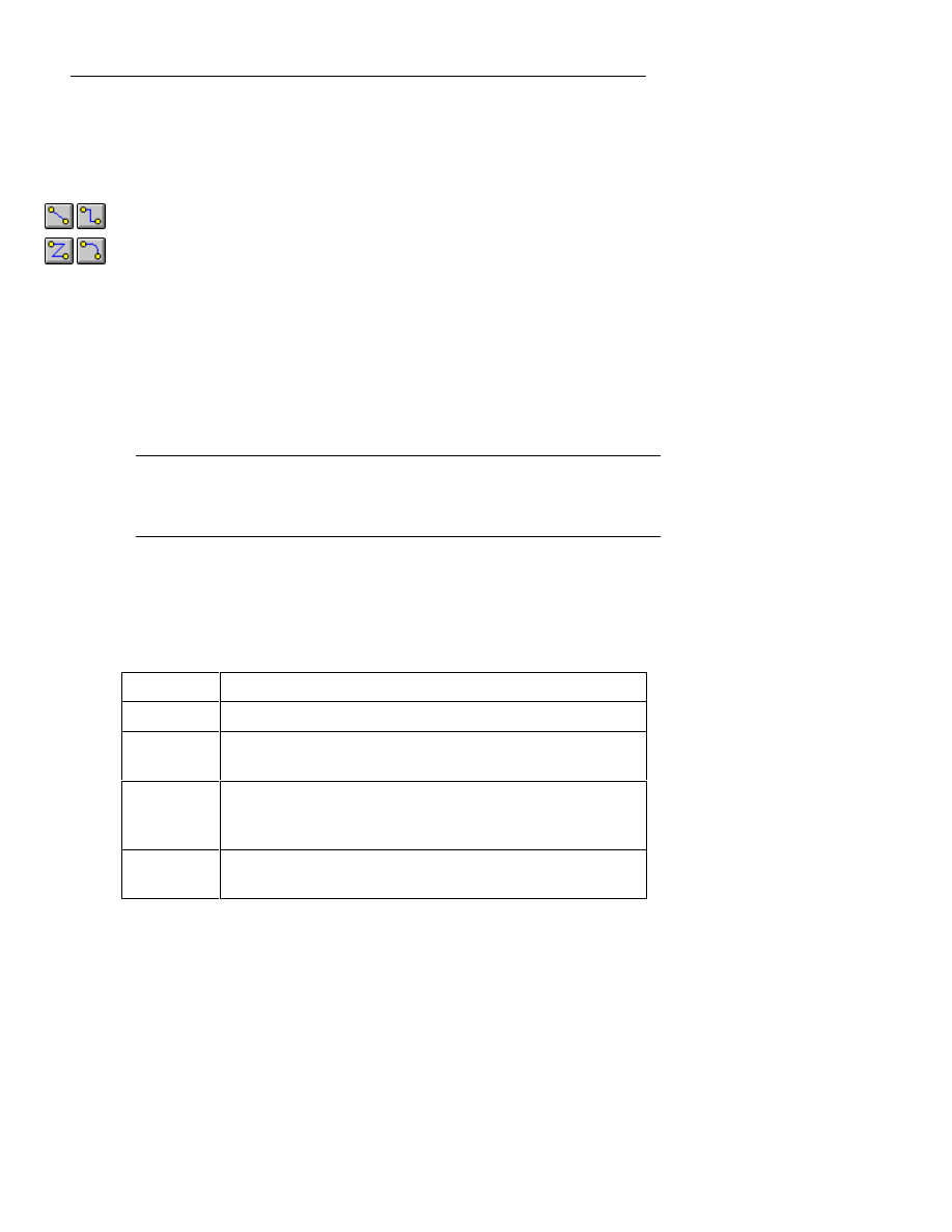
:LQ%RDUG/D\RXW5HIHUHQFH*XLGH
68
To stop placing pass marks, press
Esc
.
Track, Outline & Edge
Use Track, Outline & Edge to place tracks (copper trace), module
outlines, or board edges.
To change the Track, Outline & Edge settings, click on the Track,
Outline & Edge button. The Track, Outline & Edge dialog box displays.
For more information about changing the Track, Outline & Edge settings,
see Changing Track Settings later in this section.
Placing Tracks, Outlines, and Edges
Tracks, module outlines, and board edges are placed in a similar manner. For
the sake of simplicity, this section explains how to place tracks. You can use
the same methods to place module outlines and board edges.
F
NOTE: Before you begin routing tracks, you need to place modules. For
information about placing modules, refer to the description of the Module
and Nets & Netlist tools earlier in this chapter.
There are three methods available for placing tracks:
1.
Using single key keyboard commands to tell WinBoard how to place
tracks. Refer to the following table for the key commands and their
functions:
Key
Command Description
r
Route a track with Track, Outline & Edge routing mode.
b
Begin or continue placing vertices when placing a track,
outline, or edge.
n
End a track, outline, or edge with the
n
key. WinBoard
remains in the placement mode so you can continue placing
tracks, outlines, or edges.
Back
space
Backtrack or undo a segment while placing a track,
outline, or edge.
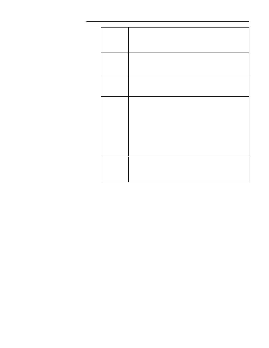
&KDSWHU0HQX5HIHUHQFH
69
c
or
-
Change to the next lower numbered layer and place a via
while routing a track by pressing
c
. Repeatedly pressing
c
will continue to change layers until the solder side is
reached.
v
or
+
Change to the next higher numbered layer and place a via
while routing a track by pressing
v
. Repeatedly pressing
v
will continue to change layers until the component side
is reached.
s
Change the style while placing a track, outline, or edge.
s
mirrors the current track, outline, or edge segments
around the location of the pointer.
w
Display the Track Parameter dialog box while routing a
track by pressing
w
. The Track Parameter dialog box
makes it possible for you to change:
1.
The track width of the track segments after the current
vertex.
2.
The via diameter of all of the vias associated with the
track after the current vertex of the track.
3.
The drill size of all of the vias associated with the track
after the current vertex of the track.
x
Toggle through the routing style with
x
: 45
°
, 90
°
, any
angle, and arc. Each time the
x
key is pressed, the Track,
Outline & Edge button changes to reflect the current
routing angle or arc.
You can change the style of track as needed as you place the track and use
any combination of styles in a single track.
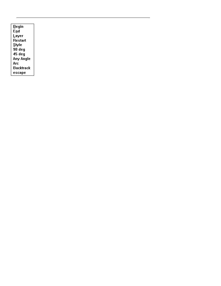
:LQ%RDUG/D\RXW5HIHUHQFH*XLGH
70
2.
Use the commands on the pop-up menu to tell WinBoard how to place
tracks. The pop-up menu looks similar to the menu at left:
You can select the options from the pop-up menu either by
clicking on the option you want or by pressing the key on the
keyboard that is underlined in the pop-up menu option.
Select Begin to begin routing a track.
Select End to end a track.
Select Layer if you want to insert a via and change the layer on
which you place the remainder of the route.
Select Restart if you want to change the layer on which you place
the route before beginning the route without inserting a via.
Select Style to change the style while routing. Style mirrors the current track
segments around the location of the pointer.
Select 90 deg if you want to change the way the track segments connect to
each other and to other objects to 90 degrees.
Select 45 deg if you want to change the way the track segments connect to
each other and to other objects to 45 degrees.
Select Any Angle if you want to change the way the track segments connect
to each other and to other objects to any angle.
Select Arc if you want to change the way the track segments connect to each
other and to other objects to an arc.
Select Backtrack to remove the most recently placed segment. You can
backtrack all the way to the beginning of the current track. If you are adding
to an already existing track, you cannot backtrack a track that has already
been parked.
Select escape to stop placing tracks.
3.
Use the left mouse button. This is the default mode to place tracks and
other objects. To select or deselect, this option, choose “Route with left
mouse button” in the
Tools | Options
dialog box. If selected, each
time the left mouse button is pressed, a track vertex is placed. You may
still use the keyboard commands in conjunction with this option.

&KDSWHU0HQX5HIHUHQFH
71
Placing the track
Follow these steps to manually place a track:
1.
To begin placing tracks, click with the left mouse button on the Track,
Outline & Edge button (or press the R hotkey). The pointer changes to:
, signifying that WinBoard has entered track routing mode.
2.
Click with the left mouse button on the layer number button for the layer
on which you want the track. You can also change to different layers by
pressing the
+
or
v
key once for each layer higher you want to go or the
-
or
c
key once for each layer lower you want to go.
You can also use
PgUp
on the numeric key pad to change to a higher layer
or
PgDn
on the numeric key pad to change to a lower layer.
3.
Place the pointer at the location you want the track to begin click with
the mouse. The pointer changes to:
, signifying that WinBoard is
ready to continue placing track segments. As you move the pointer,
notice that there is a highlighted track attached to the pointer.
F
NOTE: When you start routing inside the diameter of a pad, the track
automatically snaps to the center of the pad.
4.
Move the pointer to where you want the next vertex and click with the
mouse. The track width and color change to match the track width
settings and the color of the layer on which you are working.
5.
As you move the pointer away from the last vertex on the track, notice
that the new segment of the track is highlighted. Continue placing the
track as in step four above until you come to the location where you want
the track to end. Press the right mouse button to end the track. WinBoard
remains in routing mode so that you can continue routing tracks. To exit
routing mode, press
Esc
or click the right mouse button.

:LQ%RDUG/D\RXW5HIHUHQFH*XLGH
72
F
NOTE: To display the status of a pad, trace, via or zone, place the pointer
over the object and press the F2 key on the keyboard. This will display the
pin number and net name in the Windows status area (lower left corner of
the screen).
Vias & Routing layers (layer pairs)
The Layer buttons are also used to select which ones to toggle through. This
enables you to select only the layers you want active so you may select layer
pairs for routing. By making this selection, the program will only toggle
through the enabled layers when using the V key to drop a via.
The program defaults with the top and bottom layers selected (red).
Follow these steps:
1.
Hold down the Shift key on the keyboard and click on the layer
button with the left mouse button.
2.
The layer number will change from black to red, indicating that the
layer is active. Continue to select other layers in this same manner.
Now, when you press the V key the program will toggle through the selected
layers. When you are routing, it will allow you to select layer pairs for
routing, for example:
1.
On a six layer board, select layer 1 and layer 2 for routing layers.
2.
Start routing on layer 1 and place a via using the V key.
3.
The program will place a via and switch to layer six without having to
toggle through layers 2-5.
On a layer button that is already red, hold down the Shift key and click on the
layer button to deselect, it will change to black.
F
NOTE: You may also use the + or - keys on the keyboard to change layers, or
Page Up and Page Down. These keys will toggle through All layers on the
board regardless of the routing layers selected.

&KDSWHU0HQX5HIHUHQFH
73
Via without tracks
To place a via without tracks, follow these steps. This may be useful for
connecting ground planes, etc. Although you can use the mouse, it is easier
to use the keyboard hotkeys.
1.
Press the R key on the keyboard to start the trace/via mode.
2.
Position the pointer at the location to place the via.
3.
Press the B key on the keyboard to begin.
4.
Press the V key on the keyboard to place a via. (You can also use the +
and - keys on the ten key pad to change layers and place vias.)
5.
Press the N key on the keyboard to end.
6.
Press
Esc
to exit the place route mode.
You now have a single via, however it does not have any net information
since it is not connected to anything.
If you need to have a testpoint type object with an assigned netname, then use
a pad from the
TSTPOINT.LIB
or create your own custom pad. Place the
testpoint pad and assign a netname so that it can attach to a ground plane or
other net. To do this, use the Edit | Netlist feature and select the desired net,
then select Add Node and click on the pad to assign the net name. For more
details on assigning nets, refer to the section Edit | Netlist earlier in this
chapter.
Each testpoint pad will have the Part Value and Part Ref text. You may turn
this off globally in the Tools | Options | Object Selection dialog box, or you
can minimize the size of the text by Ctrl + double-clicking on the text and
changing the size. Do not delete this text – it is required, and do not make it
so small that it can not be selected again.
Changing Track Settings
Use Track, Outline & Edge to set the parameters in the following list and to
place tracks. To set the track parameters, click on the Track, Outline &
Edge button. The Track, Outline & Edge dialog box displays as shown
below :
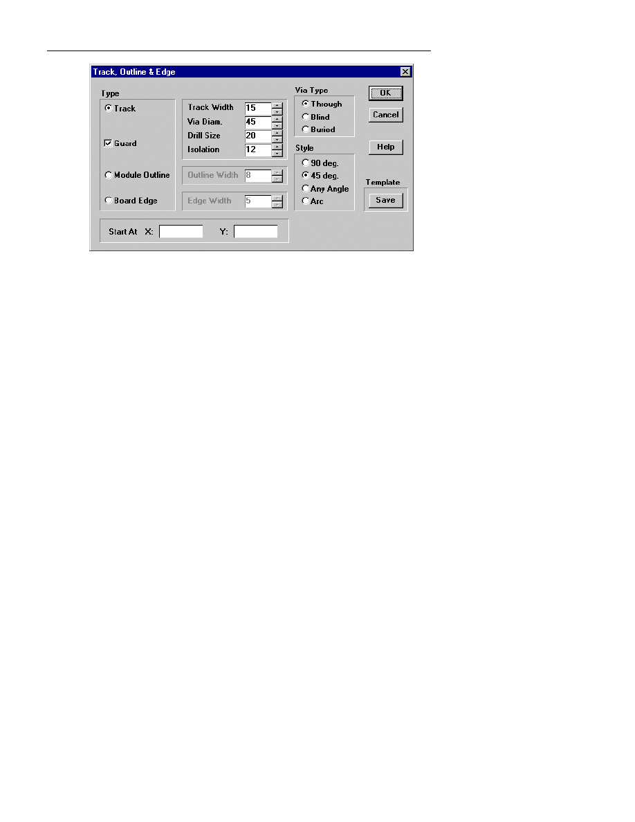
:LQ%RDUG/D\RXW5HIHUHQFH*XLGH
74
Figure 2-23.. The Track, Outline & Edge dialog box.
Use Via Type to set the via type to Through, Blind, or Buried. Select the
one you want to place.
Use Style to set the way track segments are connected to each other to 90
deg., 45 deg., Any Angle, or Arc.
Use Type to set the Track, Outline & Edge tool to place either a track, a
module outline, or a board edge.
Use Track Width, Via Diam., and Drill Size to set the width of a track, the
diameter of vias on the track, and the drill size of the vias on the track.
Use Isolation to set the radius of the routing guard. Make sure you select the
desired isolation before placing tracks. This is also used to calculate the
spacing distance of a track from a copper pour.
When you select Track from the Type section, you can choose either to use
a routing guard around pads or not to use a routing guard. A routing guard is
composed of colored lines on both sides of the track while routing. These
colored lines are the same color as the track on the layer you are routing. The
routing guard surrounds the track you are routing to show the clearance limits
for the track. The Guard check box works as a toggle. Check the box to use
a guard or remove the X if you prefer to route without a routing guard.
When you select Module Outline, the Outline Width box becomes active.
Use Outline Width to set the width of module outlines you create.
When you select Board Edge, the Edge Width box becomes active. Use
Edge Width to set the width of the board edge before you place it.
&KDSWHU0HQX5HIHUHQFH
75
Use Start At to enter exact X and Y coordinates to start the track location at
a specific location on the board. This is optional, if you do not enter a value
just click with the mouse at the desired starting point on the board.
Use OK to accept the changes you have made to the Track, Outline & Edge
dialog box and to re-display the main WinBoard dialog box.
Use Cancel to exit out of the Track, Outline & Edge dialog box without
saving any settings.
Use Help to display online help. The Help tool works similarly to online help
in other Windows-based applications.
Use Template Save to save track, outline, or edge parameters that you want
for future use.
Target
Targets are used for photographic registration of circuit boards.
Use Target to change the external and internal dimensions and style of
targets and to place targets in the board file. There are eight different target
styles available.
F
NOTE: You need only place one target on your PC board file for each
location where you need a target. WinBoard automatically places a target on
each layer of the PC board file at the same location.
The Target dialog box is shown below :
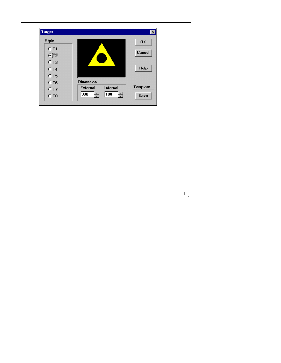
:LQ%RDUG/D\RXW5HIHUHQFH*XLGH
76
Figure 2-24.. The Target dialog box.
Use OK to accept the changes you have made to the Target dialog box and
to re-display the main WinBoard dialog box.
Use Cancel to exit out of the Target dialog box without saving any settings.
Use Help to display online help. The Help tool works similarly to online help
in other Windows-based applications.
Use Template Save to save target parameters that you want to save for future
use.
Placing Targets
To place targets after you have set the target style and dimensions:
1.
Click OK. The main drawing screen displays, the pointer changes to:
,
and a target outline appears, signifying that WinBoard has entered
placement mode.
2.
Place the target outline at the location where you want the target.
3.
Click the left mouse button.
4.
To continue placing the same type of target, move the pointer to the next
location and click the left mouse button again.
To stop placing targets, press
Esc
.
To place a different type of target, click with the left mouse button on the
Target button again and change to the appropriate target.
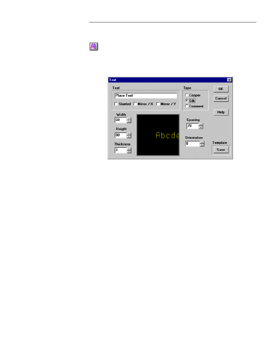
&KDSWHU0HQX5HIHUHQFH
77
Text
Use Text to enter the text string, to set the text width, height, thickness,
spacing, orientation and whether the text is slanted or mirrored around the X
or Y axis, and to place text in the board file.
The Text dialog box is shown below :
Figure 2-25.. The Text dialog box.
Use Type to set the type of text you need to copper text, silk screen text, or
comment text.
Check Slanted to set the text to be slanted or straight. An X in the check box
sets the text to be slanted. An empty check box sets the text to be straight.
Check Mirror / X to set the text to be mirrored around the X axis. An X in
the check box sets the text to be mirrored around the X axis. An empty check
box sets the text to be normal.
Check Mirror / Y to set the text to be mirrored around the Y axis. An X in
the check box sets the text to be mirrored around the Y axis. An empty check
box sets the text to be normal.
Use the up and down arrows to the right of Width, Height, and Thickness,
respectively to set the width, height, and thickness of text.

:LQ%RDUG/D\RXW5HIHUHQFH*XLGH
78
Use the up and down arrows to the right of Spacing, and Orientation,
respectively to set the spacing between letters and the orientation of the text
in degrees.
Use OK to accept the changes you have made to the Text dialog box and to
re-display the main WinBoard dialog box.
Use Cancel to exit out of the Text dialog box without saving any settings.
Use Help to display online help. The Help tool works similarly to online help
in other Windows-based applications.
Use Template Save to save text parameters that you want to save for future
use.
Placing Text
To place text after you have set the text parameters:
1.
Click OK. The main drawing screen displays, the pointer changes to:
,
and the text displays in outline form, signifying that WinBoard has
entered placement mode.
F
NOTE: While the text is still selected, you can use the left and right arrow
keys to rotate the text. You can also use the up and down arrow keys to flip
the text to the other side of the board and, at the same time, mirror the text.
If you try to flip the text on inner layers of a multi-layered board, the text will
be mirrored on the same layer it was on before you flipped it.
2.
Place the pointer at the location where you want the text to begin.
3.
Click the left mouse button.
4.
To continue placing the same text, move the pointer to the next location
and click the left mouse button again.
To stop placing text, press
Esc
.
To place a different type of text, click with the left mouse button on the Text
button again and change to the appropriate text.

&KDSWHU0HQX5HIHUHQFH
79
Module Text
With the exception of pads, to select any object that is part of a module, hold
down the
Ctrl
key while clicking with the left mouse button on the object
you want to select. Select more objects that are part of a module in the same
manner. For example, to select module text (Part Ref or Part Val) hold down
the Ctrl key and click on the text with the left mouse button. To edit module
text, hold down the Ctrl key and double click on the text to bring up the Text
dialog box.
International Characters
To place international characters, Windows must be properly configured. To
change your system configuration, select International in the Windows
Control Panel. Change the Keyboard Layout to the desired setting such as
US International. Now you may enter special international characters as text
into WinBoard.
Zone
A zone is an area on a printed circuit board that in some way represents a
signal plane or restricted area. Zones are commonly used for power and
ground planes on PC boards.
The Zone dialog box is shown next :
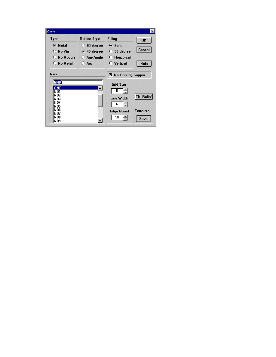
:LQ%RDUG/D\RXW5HIHUHQFH*XLGH
80
Figure 3-26.. The Zone dialog box.
Use Zone to set the zone restrictions in the following list, and to place a zone
in the board file.
•
Type:
Use Type to set the zone type to Metal, No Via, No Module, or No Metal.
•
Outline Style:
Use Outline Style to set the way the track is drawn: 90 degree, 45 degree,
Any Angle, or Arc.
•
Filling
You can use Solid, 90 degree, Horizontal, or Vertical filling for the zone.
•
Net Name:
Use Net Name to select the net with which to associate the zone. For
example : in the dialog box above GND is used to select ground.
•
No Floating Copper:
Use No Floating Copper to place copper zones without areas that are
non attached such as “islands”.
•
Grid Size:
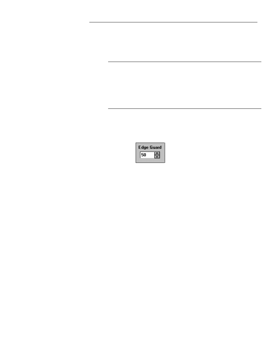
&KDSWHU0HQX5HIHUHQFH
81
Use Grid Size to set the grid size for the zone.
•
Line Width:
Use Line Width to set the width of the line used to fill the zone.
F
NOTE: The combination of grid size and line width determines how a zone is
filled—solid or hatched. As the grid size gets lower, the zone smoothes out
around NON 90 degree angles. However, the smaller the grid size, the more
memory required to display the zone. Every time you divide the grid size by
two, the memory size requirement for the zone increases by a multiple of two.
Low grid sizes also cause slower screen re-paint. Five mils is a good
compromise. The WinBoard system default is five mils.
•
Edge Guard
Use Edge Guard to select the zone isolation from the board edge. The
default setting in the box is 50. Select Place | Zone to load the Zone dialog
box. Enter the desired number directly in the Edge Guard box, or use the
arrow keys to change the setting.
The Edge Guard box
•
Th. Relief:
Use Th. Relief to set the style of thermal relief and its spoke width and guard
size. Refer to Thermal Relief in the next section for more details about
thermal reliefs.
Use OK to accept the changes you have made to the Zone dialog box and to
re-display the main WinBoard dialog box.
Use Cancel to exit out of the Zone dialog box without saving any settings.
Use Help to display online help. The Help tool works similarly to online help
in other Windows-based applications.
Use Template Save to save zone settings that you want to save for future
use.
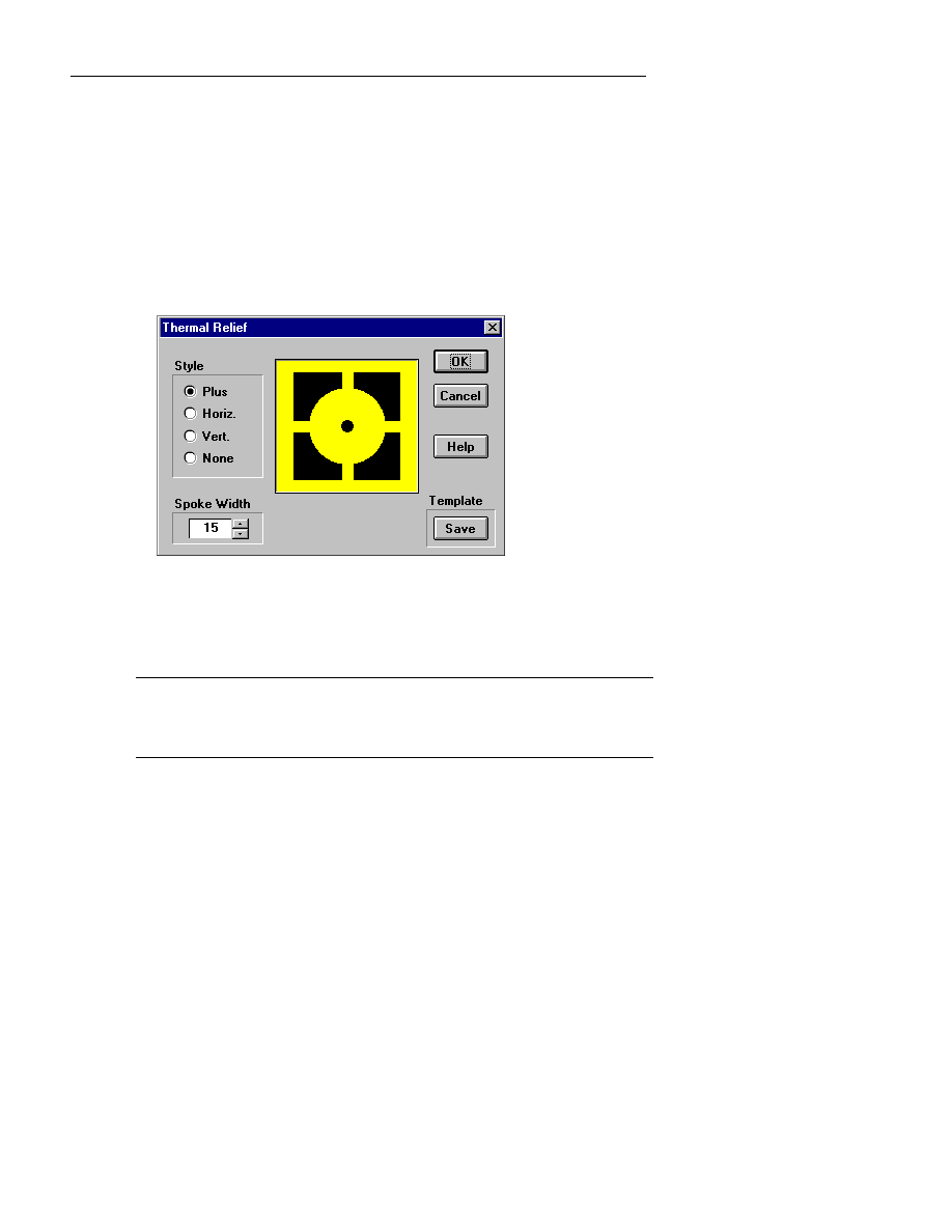
:LQ%RDUG/D\RXW5HIHUHQFH*XLGH
82
Thermal Reliefs
The Th. Relief button opens the Thermal Relief dialog box. Thermal reliefs
are used on power or ground planes around through hole and SMD pads
connected to power or ground to keep the power or ground plane from
becoming a giant heat sink when components are soldered to the PC Board
during manufacturing.
Use Thermal Relief to change the style and spoke width of thermal reliefs in
a zone.
The Thermal Relief dialog box is shown below :
Figure 2-27.. The Thermal Relief dialog box.
The figure above shows a Plus style thermal relief. There are four Style
types. Choose None to place copper completely around the pad without
using a spoke. You can change the thickness of the spokes with the Spoke
Width list boxes.
F
NOTE: If pads are close, such as smd pads, WinBoard will not place a
spoke of a Thermal Relief if it violates the isolation setting or shorts with a
nearby track or pad.
Use OK to accept the changes you have made to the Thermal Relief dialog
box and to re-display the main WinBoard dialog box.
Use Cancel to exit out of the Thermal Relief dialog box without saving any
settings.

&KDSWHU0HQX5HIHUHQFH
83
Use Help to display online help. The Help tool works similarly to online help
in other Windows-based applications.
Use Template Save to save thermal relief settings that you want to save for
future use.
Placing Zones
Follow the steps below to place a zone after you have set the zone parameters
and selected the net associated with the zone:
1.
Click OK. The main drawing screen displays and the pointer changes to:
, signifying that WinBoard has entered the zone placement mode.
2.
Click the left mouse button.
3.
Move the mouse to draw the outline of the zone. Click to place each
vertex (corner point of the zone polygon). This is done using the same
commands as placing a track segment.
4.
To complete the zone, move the pointer back to the beginning point of
the zone and double click or select End (
N
key). You do not have to
complete the polygon shape, it will automatically complete the polygon.
The zone outline is completed, thermal reliefs are placed around the pads
associated with the zone, and the zone is filled.
F
NOTE: If you prefer, you can use the
b
key for placing vertices instead of the
pull-down menu. You can also use the
x
key to toggle the outline style to
different angles just as when placing tracks. Refer to Routing Tracks in the
Getting Started Guide or Appendix C: Keyboard Commands for more
information.
F
NOTE: If you fail to return to the beginning point when you select End,
WinBoard will automatically connect the beginning and ending points with a
straight zone outline segment.
To continue placing zones, repeat the above steps.

:LQ%RDUG/D\RXW5HIHUHQFH*XLGH
84
If you get a warning that there is insufficient memory or resources to
completely fill a zone, then increase the grid size or place smaller zones. For
larger or denser boards, try placing vertical zones every 1500 mils (1.5 inches
apart). When you place multiple zones, they only need to overlap a few mils
to connect. DO NOT place zones on top of zones or overlap more than a few
mils.
Selecting and Editing Zones
To select a zone, click once on the zone. If you click inside the zone area, the
zone fill temporarily disappears and the outline becomes highlighted. You
can add, delete, and drag the zone outline vertices just as you would when
editing a track. When you have completed editing the zone outline, click on
anything to unselect the zone. In a few seconds, the newly modified zone
displays.
F
NOTE: You should NOT move, drag or modify an arc zone shape! Only edit
90 degree, 45 degree, or angles.
To change the zone parameters (such as Thermal Relief style) of an existing
zone, double-click inside the zone. The Zone dialog box displays. Make the
changes and click OK. The changes are made to the zone and the main
WinBoard screen displays.
F
NOTE: The smaller the zone grid size, the more time it takes WinBoard to
select a zone. There may be a slight delay before the zone displays as a
selected zone.
To turn off a zone to edit objects within the area, select
Setup | Object
Selection
. In the Object Selection dialog box, de-select (remove the x)
from the zone box. This turns off the zone and will make it possible to select
other objects.
Refer to Editing Zones in Chapter 1: Editing Features for more information
about selecting and editing zones.
&KDSWHU0HQX5HIHUHQFH
85
Tools
Tools contains the menu selections shown in the Tools pull-down
menu at left.
When you select an item on the Tools pull-down menu, the dialog box
for the selected tool displays.
Options
Use Options to:
•
Select the objects to view on screen.
•
Change color settings in WinBoard.
•
Insert new layers or delete existing layers.
•
Set the degrees of rotation for rotating an object.
•
Set the units for displaying the X and Y coordinates.
The Options dialog box is shown below :
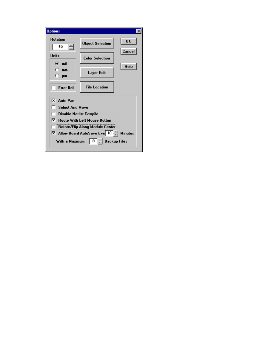
:LQ%RDUG/D\RXW5HIHUHQFH*XLGH
86
Figure 2-28. : The Setup Options dialog box.
Use Rotation to set the degrees you want to rotate an object on the
WinBoard board file. Rotation can be set in increments as small as 0.01
degrees.
Use Units to set the units for displaying the X and Y coordinates for the
current location of the pointer. You can use mils, millimeters, or
µ
m. The X
and Y coordinates for the current location of the pointer display at the right
side of the screen, just to the right of the layer name indicator.
Use Error Bell to enable or disable the error bell speaker.

&KDSWHU0HQX5HIHUHQFH
87
Auto Pan
This is used to switch on/off the programs automatic scrolling. Check this
box and the program will automatically scroll when using the Place object
commands. When Auto Pan is checked you can hold down the Ctrl key on
the keyboard to prevent automatic scrolling. Un-check this and the program
will not automatically scroll, you will need to use the manual scrolling
functions.
Select And Move
This allows an object to be selected and moved with the mouse without
releasing the left mouse button. This mode allows faster module drag and
move. Each time a module is selected and moved, the total ratsnest length
(sum of Manhattan distances of all ratsnest) is displayed in the status area (if
the netlist was compiled first).
A force vector, showing the direction for a better module placement that
would reduce the total Manhattan distance is displayed while the module is
selected and moved. This also works for a group of modules selected and
moved.
Disable Netlist Compile
Un-check this box to turn off the programs automatic netlist compile
function.
Route With Left Mouse Button
Use Route With Left Mouse Button to use the left mouse button to route.
Deselect this to use the pop-up routing menu. The keyboard shortcut keys
work with this selected or deselected.
Rotate/Flip Along Module Center
Use Rotate/Flip Along Module Center to rotate/flip modules around their
center point rather than their reference point. If this is not selected, module
will rotate around their reference (usually the center for SMD modules, and
pin 1 for through hole modules).

:LQ%RDUG/D\RXW5HIHUHQFH*XLGH
88
Auto Save
Use Auto Save function to automatically save board files. In the Setup
dialog box you may select the time for auto-backup and the number of
backups. This will save into the directory specified under Setup |
Environment. The file(s) are named
savbrdx.brd
, where x = the number
1, 2, 3, ...to 32.
Use Object Selection to select the objects on each layer to select the objects
to view on screen. For more information about how Object Selection works,
refer to Object Selection below.
Use Color Selection to change the color settings. For more information about
how Color Selection works, refer to Color Selection below.
Use Layer Edit to delete existing layers or insert new layers. For more
information about how Layer Edit works, refer to Layer Edit below.
Use File Locations to set the directory structures for different projects. For
more information about how File Locations works, refer to File Locations
below.
Use OK to accept the changes you have made to the Options dialog box and
to re-display the main WinBoard dialog box.
Use Cancel to exit out of the Options dialog box without saving any settings.
Use Help to display online help. The Help tool works similarly to online help
in other Windows-based applications.
Object Selection
Use Object Selection in the Options dialog box to select the objects to view
on screen. One exception is de-selecting zones (copper pours). Because
zones may cover large board areas, Object Selection is used to turn the zone
off visually and physically so that it may not be selected accidentally by
clicking on it with the mouse. The Object Selection dialog box is shown
below :
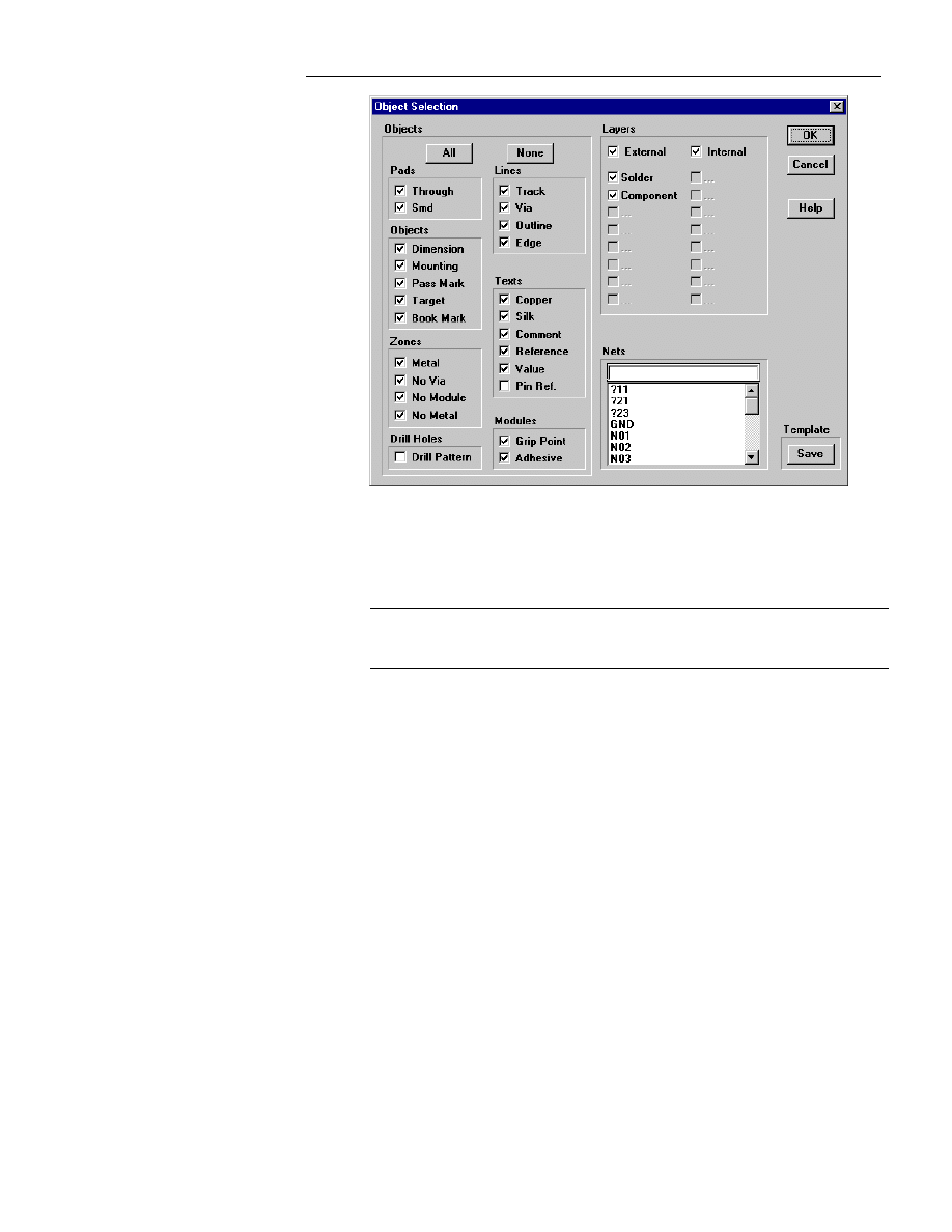
&KDSWHU0HQX5HIHUHQFH
89
Figure 2-29. : The Object Selection dialog box.
Use Object Selection to set the types of pads, tracks, text, zones, objects,
layers, and nets you view on screen. To view a particular pad, track, text,
zone, object, or layer, check the box next to it. To select a net to view, click
with the left mouse button on the net name in the Nets list box.
F
NOTE: Turning off layers in multi-layer board files can increase the screen
redraw speed.
Use All to select all of the objects to be viewed on screen.
Use None to remove every X from every check box so that none of the
objects are set to be viewed on screen.
Use OK to accept the changes you have made to the Object Selection dialog
box and to re-display the main WinBoard dialog box.
Use Cancel to exit out of the Object Selection dialog box without saving
any settings.
Use Help to display online help. The Help tool works similarly to online help
in other Windows-based applications.
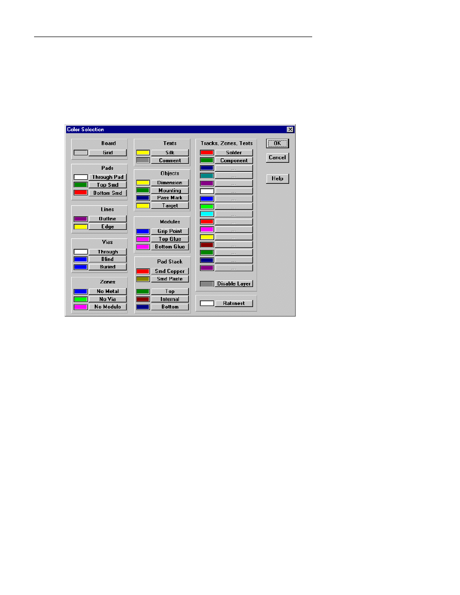
:LQ%RDUG/D\RXW5HIHUHQFH*XLGH
90
Use Template Save to save Object Selection parameters that you want for
future use.
Color Selection
Use Color Selection in the Options dialog box to change the color settings.
The Color Selection dialog box is shown next :
Figure 2-30. : The Color Selection dialog box.
To change color settings in WinBoard, select the item for which you want to
change the color by clicking on the button. The Color dialog box displays.
Select the color you want just as you would in any other Windows Color
dialog box, then click OK to accept your changes.
Use OK to accept the changes you have made to the Color Selection dialog
box and to re-display the main WinBoard dialog box.
Use Cancel to exit out of the Color Selection dialog box without saving any
settings.
Use Help to display online help. The Help tool works similarly to online help
in other Windows-based applications.
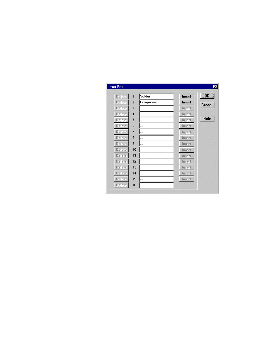
&KDSWHU0HQX5HIHUHQFH
91
Layer Edit
Use Layer Edit in the Options dialog box to delete existing layers or insert
new layers. The Layer Edit dialog box is shown below :
F
NOTE: WinBoard will not delete the solder layer. You can only delete a
layer if the layer has no components on it. You can only add or delete one
layer at a time.
Figure 2-31. : The Layer Edit dialog box.
To delete an existing layer, click with the left mouse button on the Delete
button to the left of the layer you want to delete. To accept your changes,
click on OK.
To insert a new layer follow these steps:
1.
Click with the left mouse button on the Insert button to the right of the
layer to follow the layer you want to insert. WinBoard inserts a new layer
called name.
2.
Press and hold the left mouse button while dragging the pointer across
name in the text entry box
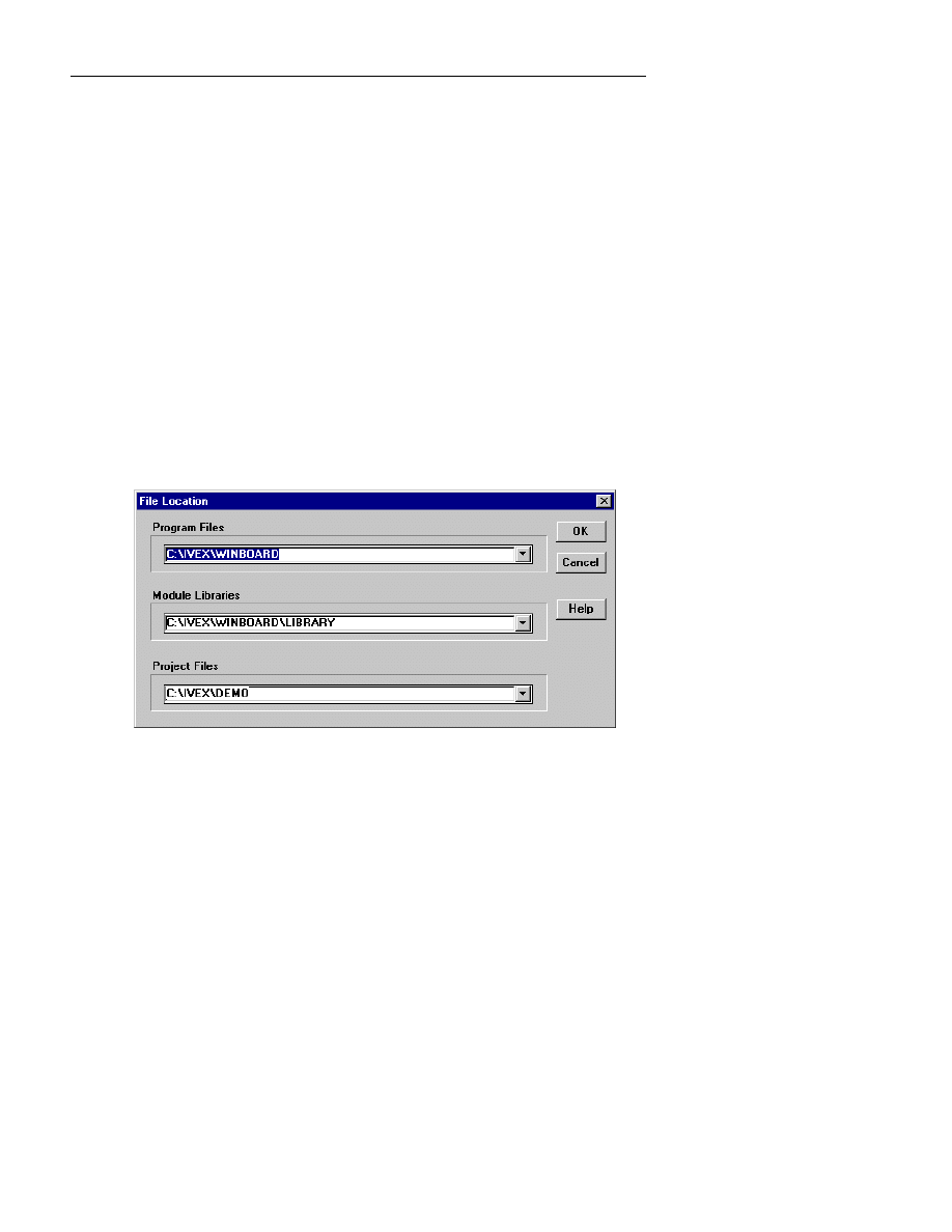
:LQ%RDUG/D\RXW5HIHUHQFH*XLGH
92
3.
Enter a name for the new layer.
4.
To accept your layer change, click on OK. WinBoard returns to the
Setup dialog box.
Use OK to accept the changes you have made to the Layer Edit dialog box
and to re-display the main WinBoard dialog box.
Use Cancel to exit out of the Layer Edit dialog box without saving any
settings.
Use Help to display online help. The Help tool works similarly to online help
in other Windows-based applications.
For each additional layer you want to add, click again on Layer Edit button
and repeat steps one through four above.
File Locations
Use File Locations in the Options dialog box to set up the directory
structures for different projects. The File Locations Directories dialog box is
shown below :
Figure 2-32. : The File Locations Directories dialog box.
WinBoard uses a project-oriented directory structure in which the files for a
particular project are all stored in a project directory separate from other
projects. WinBoard’s default directory structure looks like the directory
structure shown next :
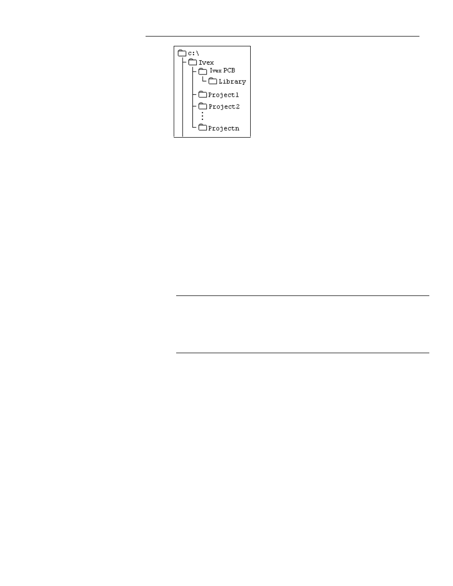
&KDSWHU0HQX5HIHUHQFH
93
Figure 2-33. : WinBoard’s directory structure.
There are three different types of WinBoard files:
1.
Program files
2.
Module library files
3.
Project files
By default, the program files belong in the
\IVEX\WINBOARD
directory,
and include all program executable files and templates. Templates have a
.tpl
file extension.
The module library files belong in the
\IVEX\WINBOARD\LIBRARY
directory by default.
The project files should be in the project directory for the project to which
they belong. Project files include board layout files, report files, print and plot
files, and any other type of output files.
F
NOTE: The program files directory and module library directories can be
located anywhere on your computer that you like, even on a different hard
drive. The
\IVEX\WINBOARD
and
\IVEX\WINBOARD\LIBRARY
directories are the default directories used when you load WinBoard onto your
computer. You can also locate the project directories anywhere you like.
To set the Program Files, Module Libraries, and Project Files directories,
follow these steps:
1.
Highlight the name of the program file, module library file, or project file
directory you want to use, or enter a new directory name in the
appropriate list box.
2.
Click OK. The changes are accepted and the Options dialog box
displays.
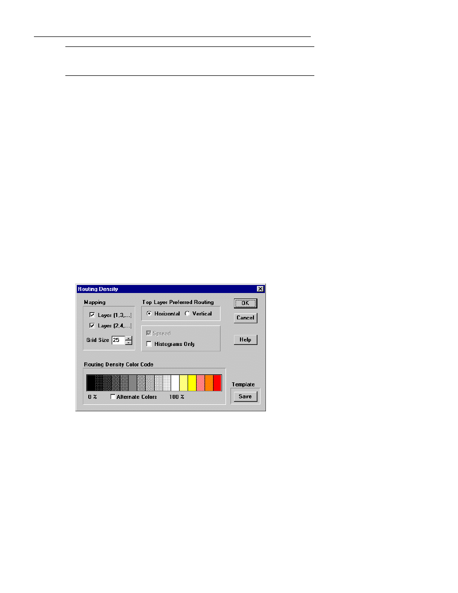
:LQ%RDUG/D\RXW5HIHUHQFH*XLGH
94
F
NOTE: The Program Files, Module Libraries, and Project Files directory
list boxes are limited to eight entries per list box.
Use Cancel to exit out of the Options Directories dialog box without saving
your changes.
Use Help to display online help. The Help tool works similarly to online help
in other Windows-based applications.
Density Map
Density Maps and Histograms use various color shadings to indicate areas of
the board with the greatest concentration of potential routes. The user can
then move modules to allow more room for routing. While moving the
modules, WinBoard recalculates and moves the ratsnest and force vector
associated with a module as it is repositioned. Using the ratsnest as a guide,
the designer may rotate and move the modules to the optimal position. With
the “total sum” of the ratsnest, the user can optimize the board by placing the
modules with the least sum total. All of these items are designed to assist
with placement.
To use Density Maps, first compile the netlist. Then, choose
Tools |
Density Maps
from the WinBoard menu or press the “
I
” key on the
keyboard. This will load the Routing Density dialog box as follows:
Figure 2-34.. The Routing Density dialog box.

&KDSWHU0HQX5HIHUHQFH
95
Use Mapping to select the layers and grid size. Place an
X
in the appropriate
layer box to show a density map for odd number layers (1,3,5...) or even
number layers (2,4,6...) or both.
The default Grid Size is 25 mils. The smaller the grid size, the longer it will
take to calculate the density map for the board. Likewise, the more you zoom
out to view a larger board, the larger the grid size will need to be in order to
be visable. In order to view the density map for a larger board, it may
necessary to select a grid size such as 50 mils or more.
Use the Top Layer Preferred Routing to select either horizontal or vertical.
If you plan to route the top layer horizontally, select horizontal to compute
the density map with horizontal routing preferred on the top layer.
Use Histograms Only to view the histogram without viewing the density
map.
The Spread option is for future use. When implemented, it will allow
density map calculations if routing is allowed outside the rectangle (see
description of density map below).
Use the Routing Density Color Code to select the color pattern you wish to
use to show various densities on the board. The default colors start at black
for zero percent and go from shades of dark gray to light gray to white at 100
percent. Click on the box marked Alternate Color for a second choice of
colors. The default selection for Alternate color is black for everything less
than 100 percent. To change any color, click on the density gradient with the
left mouse button. This will open a color dialog box. Click again with the
left mouse on the desired color and press OK to make the change. You may
save the color selections by using the Template Save button.
Press OK to display the density map and histogram on the board file.
Press Cancel to remove the density map and/or histogram from the board
file.
Use Template Save to save the settings such as new color selections.
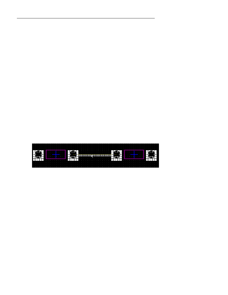
:LQ%RDUG/D\RXW5HIHUHQFH*XLGH
96
Description
The percentages refer to the total required track width and pad size at any
given interval divided by the size of the interval. The interval is equal to the
grid size. The density area is in reality a rectangle with the height equal to
the chosen grid size. For each grid increment, there is a certain probability
that a given track would cross, this probability equals the width of the track
divided by the horizontal dimension of that enclosing rectangle. A pad would
always occupy its space with a 100 percent probability. The probability is
defined as:
(
track width + isolation)/(grid size/layers)
So, the density map itself depends on the preferred routing (vertical or
horizontal) given to each layer. A probability refers only to the grid size.
The board would be unroutable only if the average probability on every cell
of the horizontal or vertical crossing lines would exceed 100 percent over a
large portion of the board.
Examples
In the example below, one net is represented on a 2 layer board. The shading
is medium gray representing 50 percent. If the density map were calculated
for only even layers, then this line would be white or 100 percent because
you would not route on the solder layer.
Figure 2-35.. Example 1.
Continuing the example above, add another net connecting the other two
pads and rotate one of the capacitors about 15 degrees. Notice that the area
representing the path of the farthest two pads is medium gray, however now
the overlapping area representing the path now occupied by two possible nets
is white because there is a 100 percent probability of a track in this area.
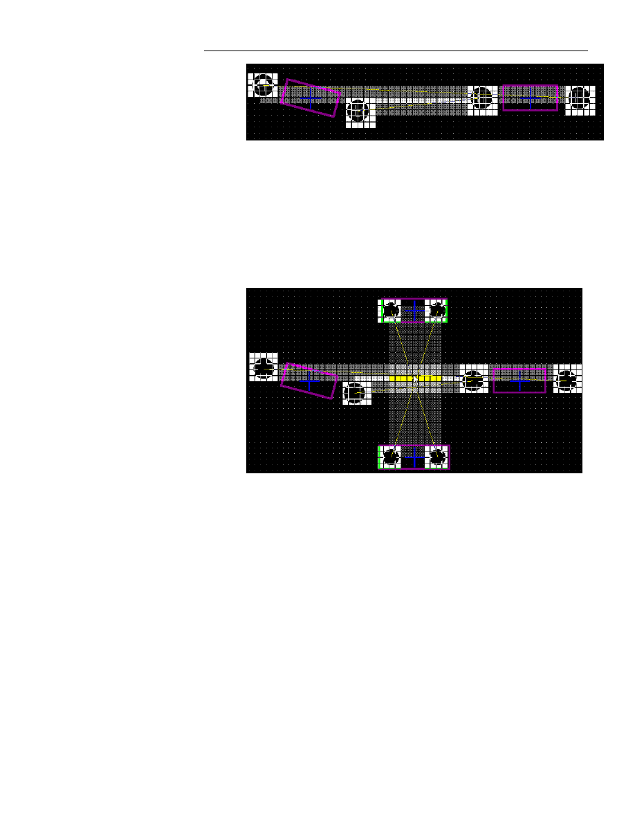
&KDSWHU0HQX5HIHUHQFH
97
Figure 2-36.Example 2.
Add a few more modules and nets to the example. Now the area at the very
center where all the paths cross turns to yellow, representing 120 percent
density. (In the printed black and white manual, this center area where the
arrow points shows as gray, but you can try this example for yourself and see
the color change.) This area represented by the yellow density map is a
potentially difficult area to route.
Figure 2-37.. Example 3.
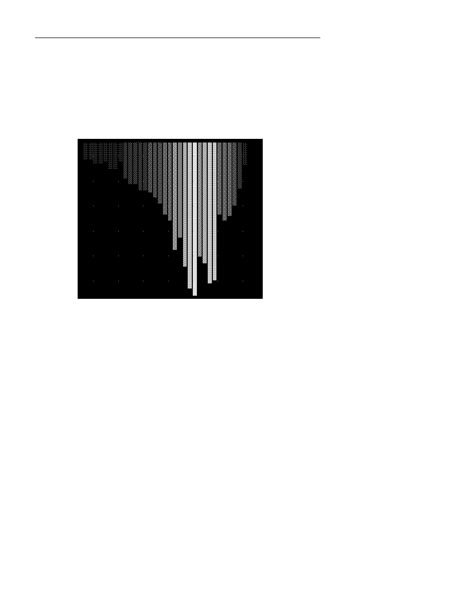
:LQ%RDUG/D\RXW5HIHUHQFH*XLGH
98
Histograms
The histograms display dense areas on the board represented by the color and
height of the bar associated with a certain grid. Each histogram bar
corresponds to the sum of all routing probabilities of the corresponding board
cross section, divided by the cross section size. The size is the number of
grid increments. The light colors (almost white) on the histogram below
represents potentially difficult grid areas on the board to route.
Figure 2-38.. Histogram.
The density map and histogram may also be printed. In the
Print |
Object Selection
dialog box, click on Density Map. Use the Preview
feature to make sure you choose an appropriate scale. For more information,
refer to the section in the manual on printing.
AutoPlace
This is a grayed out option and is not available with this version of
WinBoard.

&KDSWHU0HQX5HIHUHQFH
99
AutoRoute
Use AutoRoute to launch the interface to the Specctra autorouter. The
interface is used to configure your settings for Specctra to autoroute the
board. Once the interface is configured with the desired settings, you may
proceed to route the board if you own a copy of the Specctra autorouter.
You must have Specctra installed with a valid license. If you do not own
Specctra contact Ivex or your Ivex distributor for pricing.
See Chapter 5 for details on using the Specctra Interface.
Load Routed Board
Use Load Routed Board to open the board file routed with the Specctra
autorouter. If you own the Specctra autorouter and completed routing a
board file with it, use this option to open the routed board file.
This option restores the netlist parameters to the routed board. Some
versions of Specctra leave the netlist parameters out of the completed board
and you must use this option to properly restore these values. Be sure to
Save the file after loading it so that the file is saved with the proper netlist
information.
Netlist
Use Nets & Netlist to display ratsnests. A ratsnest is a term used to describe
the line connecting two or more pads that are part of the same net, but not
physically routed with copper traces.
To change the Nets & Netlist parameters, and to select ratsnests to display,
click on the Nets & Netlist button. The Nets & Netlist dialog box displays.
The Nets & Netlist dialog box is shown below :
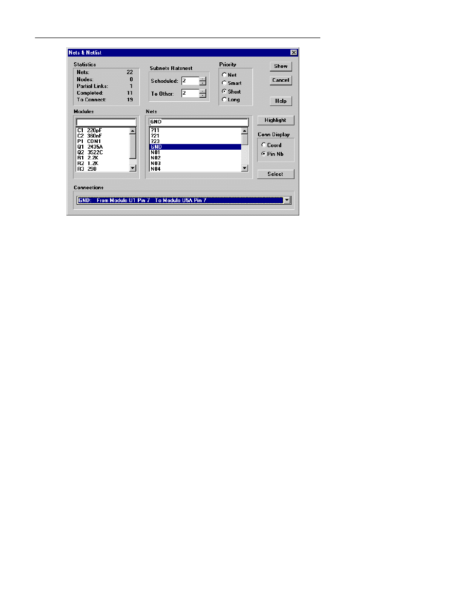
:LQ%RDUG/D\RXW5HIHUHQFH*XLGH
100
Figure 2-39.. Nets & Netlist dialog box.
Use Statistics to monitor the total number of:
•
Nets on the board.
•
Nodes on the board—pads to which the net should connect.
•
Partial Links that have been routed. Partial links are partially routed.
Partial routes are also known as parked routes.
•
Completed nets—the number of completed connections between two
nodes.
•
To Connect—the number of connections between two nodes that need
to be completed.
Use Subnets Ratsnests to determine how many scheduled and other ratsnests
to display. A Scheduled ratsnest is the next connection in the net closest to
the pad you are routing from. To Other refers to the connections in the net
other than the scheduled ratsnests. You can set the number of scheduled and
other Subnets Ratsnests to any number you like. Scheduled ratsnests are
yellow, while other ratsnests are green.
Use Priority to determine the priority used to route with More Connections
and to list ratsnests in the Connections list box. Refer to More Connections
and Connections below. The options are:

&KDSWHU0HQX5HIHUHQFH
101
•
Net—rank connections by net.
•
Smart—rank connections for an optimal layout.
•
Short—rank connections by length, shortest first.
•
Long—rank connections by length, longest first.
Use Modules to display all ratsnests for the module you select from the
Modules list box. The default is for the nets on all modules to be displayed
unless you select a particular module.
Use Nets to select a particular ratsnest you would like displayed. The default
is for all of the nets to be displayed unless you select a particular net.
Use Conn Display to set the method for displaying pin locations of
connections in the Connections list box: Use Coord to display the (X, Y)
locations and layer of the pins, and Pin Nb to display the module name with
pin numbers.
Use Connections to show or select the connections to display that remain to
be routed. The Connections list box lists the remaining connections, in the
order specified in the Priority box, for one of the following:
•
All nets on the board file. To view the list of remaining connections on
the whole board file, leave the Modules and Nets text entry boxes empty
and click with the left mouse button on the Connections list box.
•
All the nets for a particular module. To view the list of remaining
connections for a particular module, select the module for which you
want to view remaining connections from the Modules list box and click
with the left mouse button on the Connections list box.
•
One particular net. To view the list of remaining connections for a
particular net, select the net for which you want to view remaining
connections from the Net list box and click with the left mouse button on
the Connections list box.
Use Show to return to the main WinBoard screen and display all the ratsnests
or the modules or nets you selected.
Use Highlight to highlight all of the tracks in a particular net that have
already been routed.
Use Select to route a particular connection from the Connections list box as
follows:
1.
Click with the left mouse button on the Connections list box. The
Connections list box expands so you can see all of the connections.
:LQ%RDUG/D\RXW5HIHUHQFH*XLGH
102
2.
Click with the left mouse button on the connection in the list that you
want to route. WinBoard highlights the connection in the Connections
list box.
3.
Click with the left mouse button on Select. The main WinBoard screen
displays in track routing mode with the track already started on the first
pin.
4.
Continue routing the track.
Use Cancel to exit out of the Nets & Netlist dialog box without saving any
settings.
Use Help to display online help. The Help tool works similarly to online help
in other Windows-based applications.
More Connections
Use More Connections with Nets & Netlist to select the next connection in
the Connections list. First, select a connection from the Connections list box
in the Nets & Netlist dialog box. Then, when you are ready to move on to the
next net, simply click once with the left mouse button on the More
Connections tool. The ratsnest for the next connection listed in the
Connections
list box of the Nets & Netlist dialog box displays.
WinBoard determines the order in which to list the connections in the
Connections list box by the Priority you select in the Priority box. Refer to
Priority above for more information.
F
NOTE: You can press the
m
key instead of clicking on the More
Connections tool button. Each time you press the Esc. key followed by the m
key, WinBoard increments to the next connection.
CAM
CAM contains the menu selections shown in the CAM pull-down
menu at left.
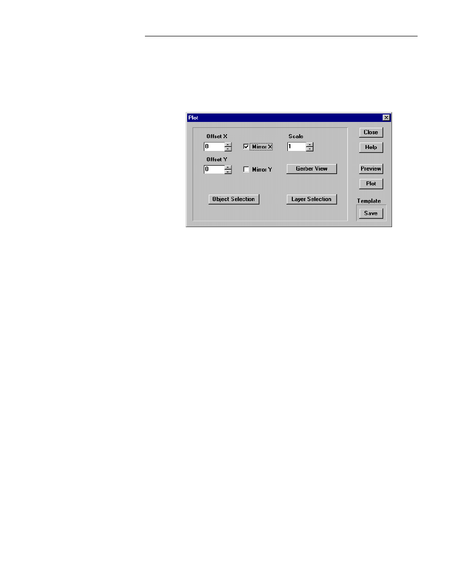
&KDSWHU0HQX5HIHUHQFH
103
Photo Plot
Photo Plot produces Gerber photo plot files for production of the PC board.
When you select Photo Plot from the CAM menu, the Plot dialog box
displays. The settings in the Plot dialog box work the same for Photo Plot as
for other types of printing and plotting.
Figure 2-40. : The Plot dialog box.
Object Selection
Press the Object Selection button to select the object to photo plot on each
layer. Use the buttons on the left side of the dialog box that are pre-
configured for Copper, Silk, SMD Paste, Adhesive, Drill and Solder Mask.
To manually select objects, use the individual check boxes.
Press All to select every object on the board. This will select each object
except for the Density Map and Paste.
Press None to uncheck the boxes so that you can manually check the
individual boxes.
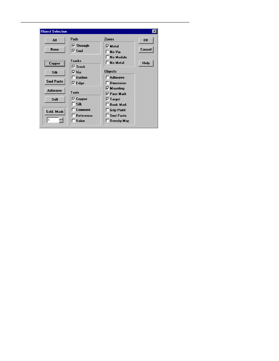
:LQ%RDUG/D\RXW5HIHUHQFH*XLGH
104
Figure 2-41.. Object Selection.
When you press the Copper button, it will automatically select the objects
associated with copper on the board. This includes copper traces, pads and
copper zones.
When you press the Silk button, it will automatically select the silk screen
objects for the specified layer. This includes the module outline, board edge
and module text. If you do not want the Part Reference or Part Value
associated with each module to print, manually uncheck the box next to these
items.
SMD Paste produces an image of the “solder paste” for all SMD pads on the
board which have a solder paste object associated with them. See the MCL
language or Pad Stack editor sections on how to specify solder paste for an
SMD pad.
Press the Drill button to generate a drill drawing for the board. (This is not
an NC Drill report which is located in the
CAM | NC Drill
menu) The
Drill feature is used to assign a unique symbol to each drill hole on the board.
It will open the following dialog box:
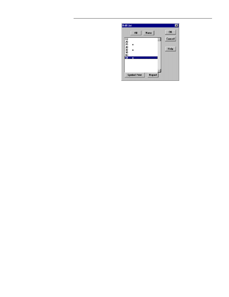
&KDSWHU0HQX5HIHUHQFH
105
Figure 2-42.: Drill List.
In the dialog box above, each number represents a drill hole on the board.
Press the All button to assign a drill symbol to each drill hole on the board.
An asterisks will display next to each drill number.
Press the None button to remove the asterisks next to each drill number.
Click on the number of each drill number to manually select each drill
symbol you want to display. An asterisks will display next to the number you
select.
Press OK to generate a drill drawing for the selected drills. When you print
(File | Print) this layer, a unique drill symbol will display for each drill hole.
Press the Symbol Print button to print a report legend. This will list the
board name and a list of all drill symbols selected followed by the drill hole
diameter.
Press the Report button to open the NC Drill dialog box.
Solder Mask produces an image of every solderable pad on the board,
enlarged by the number located below the Solder Mask button. When
reversed, this output depicts the protective layer of solder mask for the board.
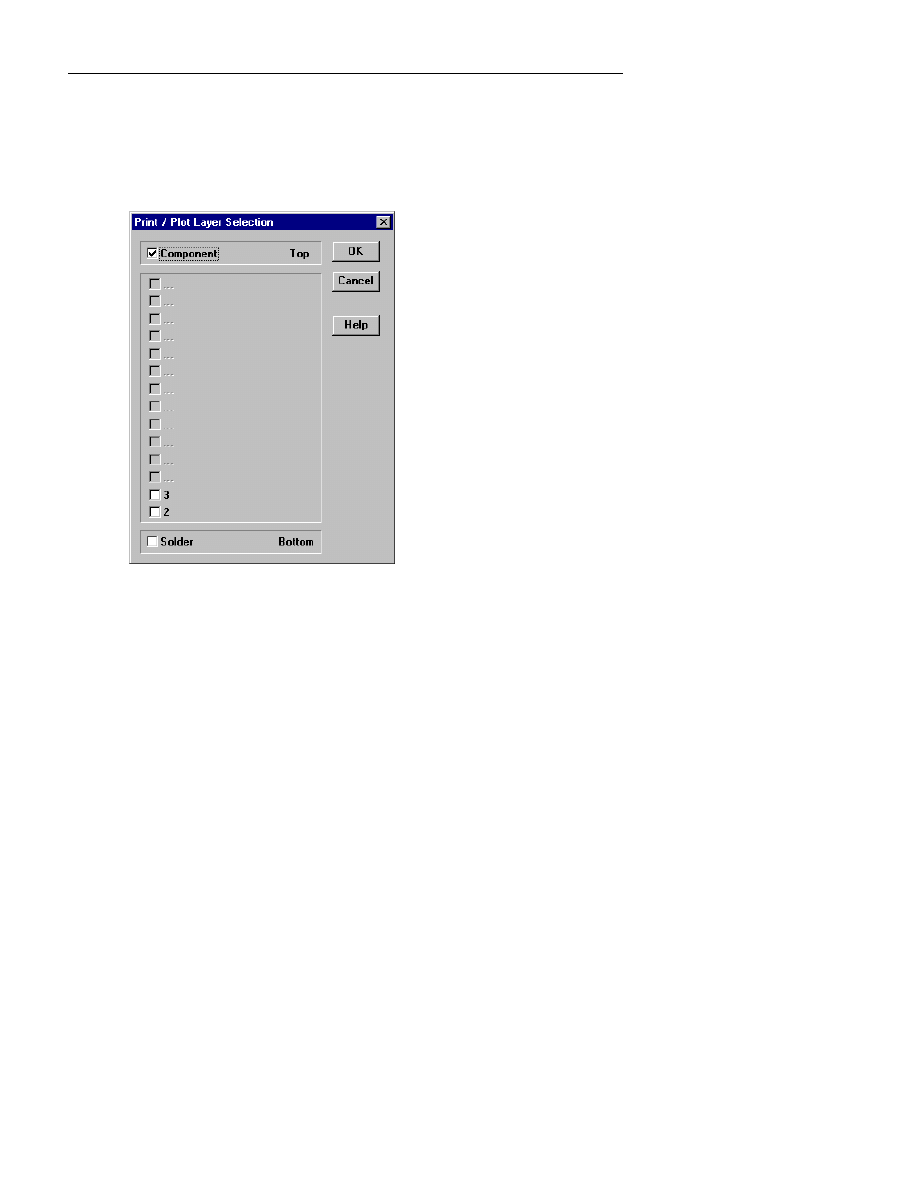
:LQ%RDUG/D\RXW5HIHUHQFH*XLGH
106
Layer Selection
Press the Layer Selection button to select each layer on the board that you
need to generate Gerber photo plot for. You will need a separate photo plot
to make film for each copper and silk layer. In the layer dialog box, click on
the layer you are generating film for.
Figure 2-43.:The Print Layer Selection.
The example layer dialog box shown above is for a four layer board. The
four available layers are Component, Solder, layer 2 and layer 3.
Gerber View
If you own a copy of the Ivex View Gerber viewer and have it installed on
your computer, press the Gerber View button. This will automatically
generate a Gerber 274-X photo-plot output for the selected objects and
launch the file for viewing in Ivex View.
Use the Object Selection and Layer Selection buttons to select the desired
objects to view. Check the Mirror X box to view the Gerber file in the same
orientation as the board on your screen.
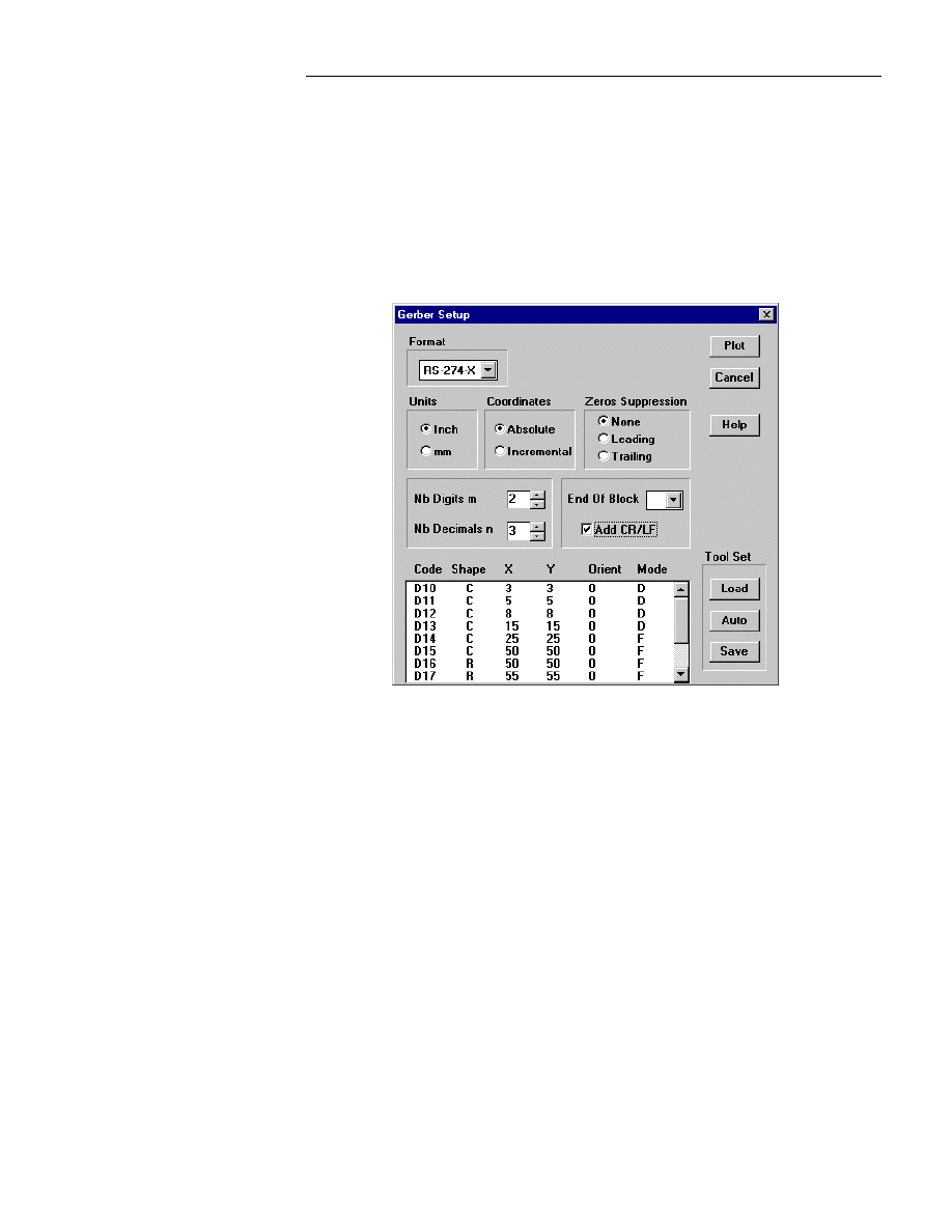
&KDSWHU0HQX5HIHUHQFH
107
Preview
The Preview button displays a printer preview of the selected board
components. Use the Object Selection and Layer Selection buttons to
select the desired objects to view. This is not the same as a Gerber Viewer.
Plot
When you click the Plot button in the Plot dialog box, the Gerber Setup
dialog box displays as shown next:
Figure 2-44. : The Gerber Setup dialog box.
Use Format to specify the plot format. RS-274-D is the old Gerber format
and requires a separate aperture table. Refer to Tool Set later in this section
for details generating an aperture list. Select RS-274-X to generate the newer
Gerber format that includes the aperture list. RS-274-X is the recommended
format because it includes the aperture list in the Gerber file, and it supports a
much greater number of apertures.
Some advantages for using the 274-X Standard:
1.
You do not have to manage two files, a Gerber and a D-Code file.

:LQ%RDUG/D\RXW5HIHUHQFH*XLGH
108
2.
It is not limited to 24 or 99 apertures as 274-D.
3.
Pads may be rotated at any angle while 274-D only supports 90
degrees.
Because of the limitation of the old 274-D format, you should insist on using
a manufacturer that supports the 274-X format for the best and most reliable
results.
Use Units to set the output units to inches or millimeters.
Use Coordinates to set the output coordinates to absolute or incremental
mode. Absolute is the default setting.
Use Zero to set Gerber photo plotting to omit trailing zeros or leading zeros,
to omit both trailing and leading zeros, or to include zeros. Check Leading to
omit leading zeros. Check Trailing to omit trailing zeros.
Use Nb Digits m to set the number of digits before the decimal point. The
standard setting is 2.
Use Nb Decimals n to set the number of digits after the decimal point. The
standard setting is 3.
Use End Of Block to set the end of block string.
Check Add CR/LF to use carriage returns with line feeds in the output file.
It is usually easier to read the file with this option checked.
F
NOTE: Check with your plotting service or film maker to get the correct
parameters for their equipment before generating a Gerber output.
Aperture Tool Set
Use Auto in the Tool Set box to automatically generate an aperture list from
the current board.
Use Load in the Tool Set box to load the aperture list from a file. For more
information about Tool Set definitions, refer to Custom Gerber Tool Set
Definitions below.
Use Save in the Tool Set box to save the generated aperture list to a file.
Use the Aperture Table list box to view the existing aperture parameters.
The aperture parameters are defined as follows:
Code
The D-Code for the aperture
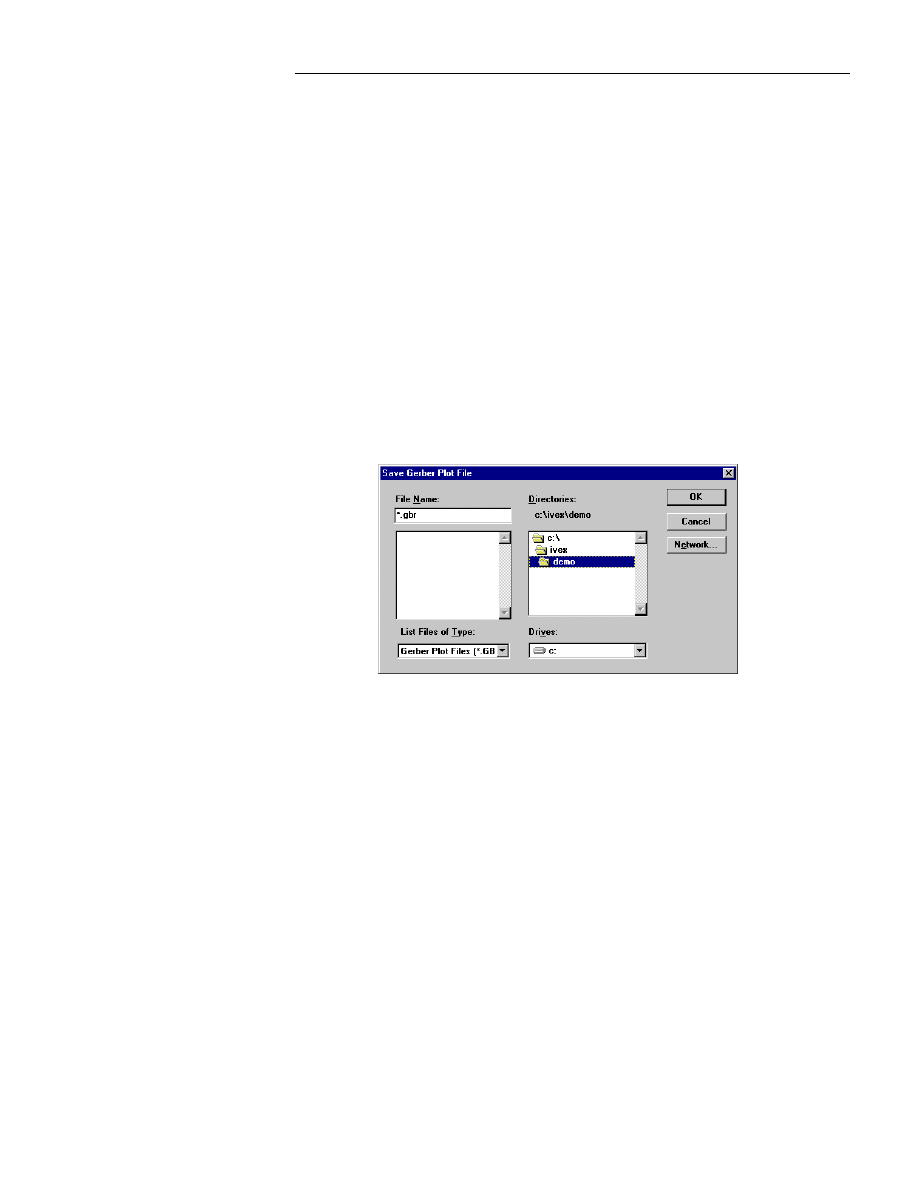
&KDSWHU0HQX5HIHUHQFH
109
Shape
The shape of the aperture:
C
for Circle aperture
R
for Rectangle aperture
X
Diameter of the aperture in the X direction
Y
Diameter of the aperture in the Y direction
Orient
The rotation of the aperture
Mode
Mode or method of flash:
D for Draw
F for Flash
B for Both
When you click Plot in the Gerber Setup dialog box, the Save Gerber File
dialog box displays. Enter a file name under which you want your Gerber
photo plot file saved, select the appropriate directory, and click OK.
Figure 2-45.: Save Gerber Plot File
Use Cancel to ignore any changes you have made to the settings, and display
the Print/Plot dialog box.
Use Help to display online help. The Help tool works similarly to online help
in other Windows-based applications.

:LQ%RDUG/D\RXW5HIHUHQFH*XLGH
110
Instructions on using Gerber
The Photo Plot feature is used to make a Gerber output for each layer of the
board. Some layers, such as the Component layer, usually require multiple
outputs because different sets of film are used for items such as copper, silk,
and paste. Following is the step by step process:
1.
Select CAM then Photo Plot from the menu. This opens the Plot dialog
box.
2.
Select Layer Selection to open the layer selection dialog box. A separate
Gerber file must be generated for each layer. Choose the desired layer
and press OK.
3.
Select Objects Selection and choose the desired objects. Press the
Copper button to automatically select the items necessary for a copper
output. It is usually necessary to generate a copper output for each layer
of the board. Press Ok to return to the Plot dialog box.
4.
After selecting the layer and objects, press Plot. This opens the Gerber
Setup dialog box.
5.
Select the appropriate settings. Use the format RS-274-X to generate a
Gerber file with the aperture included—this is the default setting. You
should ask your film and board manufacturer for what specific settings to
check in this dialog box.
6.
When the appropriate setting have been entered, press Plot. Enter the
output file name and press OK. Typical file extensions are .ger and .gbr,
however you can enter any 3 digit file extension.
Repeat steps 2 through 6 to generate a Gerber file for each layer. Use a new
file name such as layer1.ger, layer2.ger or solder.ger, comp.ger.
Custom Gerber Tool Set Definitions
You can create your own custom Gerber tool set definitions in an ASCII text
file. This section explains how.
F
NOTE: The custom Gerber tool set file must use the same type of parameters
and in the same order as those used in the Aperture Table list box.
The first four lines of all custom Gerber tool set files must be in the following
format:

&KDSWHU0HQX5HIHUHQFH
111
Line 1:
Ivex;
Line 2:
Unit: mm or mil;
Line 3:
m:8; n:3;
Where:
m
is the number of digits before the decimal point and
n
is the
number of digits after the decimal point.
Line 4 and following are aperture definitions. The following figure shows an
example custom Gerber tool set file.
Ivex
Unit: mil;
m:3;n:2;
D10
C
55
55
F;
D11
R
35
25
F;
D12
C
25
25
D;
D13
C
60
60
B;
Figure 2-46.: An example custom Gerber tool set file.
NC Drill
Use NC Drill to automatically produce Excellon NC Drill files for through
holes and blind and buried vias for specific layer pairs.
NC Drill generates NC Drill files used to drill the PC board during the
manufacturing process. NC Drill groups pads into through holes, blind vias,
and buried vias. Blind vias and buried vias are then separated further into
layer pairs by via type. For example, if blind vias reside on layer pair 1 and 2,
and layer pair 5 and 6, two drill files are created for all the blind vias. If
buried vias exist, drill files are created by layer pairs in the same way drill
files are created for blind vias.
Each drill file produced by NC Drill uses the file name specified by you,
with the following file name extensions:

:LQ%RDUG/D\RXW5HIHUHQFH*XLGH
112
.DRL
This file lists the date the file was created, the version of
WinBoard used to create the file, the name of the output file, the
names of all the drill files produced for the current board, the drill
tools needed to drill the board during manufacturing, the drill
count for each file, and the tool size and layer pairs for each drill
file.
.TH
This file lists all of the through holes on the board file.
.L?
This file lists all blind vias for a layer pair. A separate file is
generated for each layer pair that contains blind vias. The
?
denotes the sequential number for each report. For example, for a
board file that has blind vias on layers 1 and 2, and on layers 5
and 6, NC Drill generates files with the following file extensions:
•
.L1
—This file lists the blind vias on layer pair 1, 2.
•
.L2
—This file lists the blind vias on layer pair 5, 6.
.U?
This file lists all buried vias for a layer pair. A separate file is
generated for each layer pair that contains buried vias. The
?
denotes the sequential number for each report. For example, for a
board file that has buried vias on layers 2 and 3, and layers 4 and
5, NC Drill generates files with the following file extensions:
•
.U1
—This file lists the buried vias on layer pair 2, 3.
•
.U2
—This file lists the buried vias on layer pair 4, 5.
.PUN
This file lists all punch holes or NC Drill holes on the board file.
When you click on NC Drill, the NC Drill dialog box displays as shown
below:
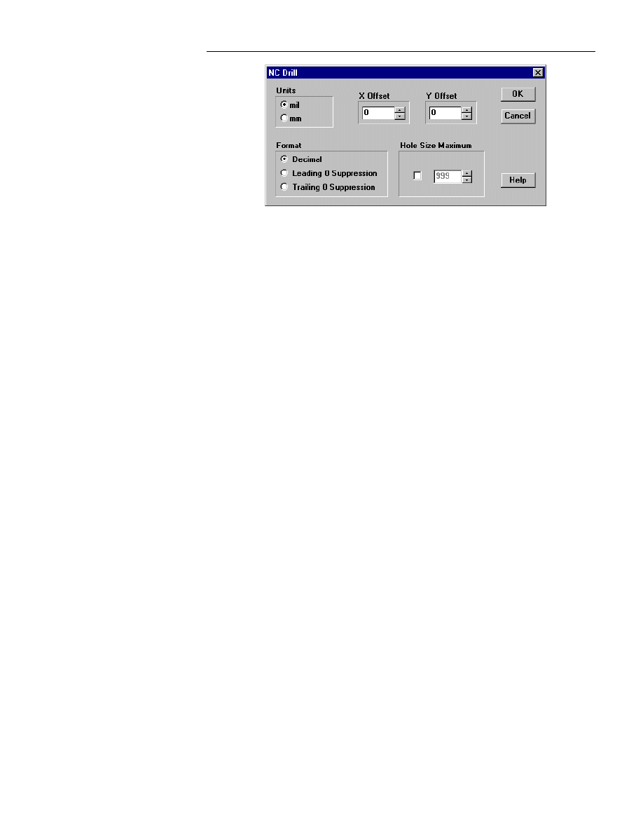
&KDSWHU0HQX5HIHUHQFH
113
Figure 2-47.: The NC Drill dialog box.
Use Units to set the output units to inches or millimeters.
Use Format to set the format to decimal, leading zero, or trailing zero.
•
Decimal produces NC Drill files in Excellon decimal format.
•
Leading 0 produces NC Drill files in Excellon decimal format.
•
Trailing 0 produces NC Drill files in Excellon decimal format.
Use X Offset and Y Offset to set offsets for X and Y coordinates. The
default for both X Offset and Y Offset is zero.
Use Hole Size Maximum to set the maximum hole size for the NC Drill
report. Any holes over the size specified here are reported in the
.PUN
file.
The Hole Size Maximum check box must be checked if you want the drill
report to have a maximum hole size. Otherwise, no maximum hole size is set.
Use OK to accept the changes you have made to the NC Drill dialog box and
to re-display the main WinBoard dialog box.
Use Cancel to exit out of NC Drill without saving any settings.
Use Help to display online help. The Help tool works similarly to online help
in other Windows-based applications.
An example of how to use NC Drill follows.
Assume the following:
•
TEST.BRD
is a six layer board.
•
TEST.BRD
contains all through hole components.
•
Through vias are used.
•
Blind vias are used on layer pair 1 and 2 and layer pair 5 and 6.

:LQ%RDUG/D\RXW5HIHUHQFH*XLGH
114
•
Buried vias are used on layer pair 3 and 4 and layer pair 4 and 5.
To run NC Drill, on the current board, you would follow these steps:
1.
Click on CAM. The CAM pull-down menu displays.
2.
Click on NC Drill. The NC DRILL dialog box displays.
3.
Select the appropriate settings as described above and click OK.
The Save NC Drill Report dialog box displays.
4.
Type
TEST
in the File Name: text entry box and select the
appropriate directory from the Directories: list box.
5.
Click OK. NC Drill creates these files:
TEST.TH
This file contains a list of all the through hole
pads and vias.
TEST.L1
This file contains a list of all the blind vias of the
first layer pair encountered—either layers 1 and
2, or layers 5 and 6.
TEST.L2
This file contains a list of all the blind vias of the
next layer pair encountered.
TEST.U1
This file contains a list of all the buried vias of
one layer pair—either layer 3 and 4, or layer 4
and 5.
TEST.U2
This file contains a list of all the buried vias of
the layer pair NOT listed in
TEST.U1
.
TEST.DRL
This file lists the date the file was created, the
version of WinBoard used to create the file, the
name of the report file, the names of all the drill
files produced for the current board, the drill
tools needed to drill the board during
manufacturing, the drill count for each file, and
the tool size and layer pairs for each drill file. A
sample of the data in
TEST.DRL
is shown
below.
TEST.DRL sample output:
NCDrill generated by WinBoard V1.00 Date Created:
4/18/1994
NCDrill Report File: test.drl

&KDSWHU0HQX5HIHUHQFH
115
Through Hole File Name: TEST.TH
Tool 1:
0.015
10 holes
Tool 2:
0.025
66 holes
Tool 3:
0.050
3 holes
Blind Via File Name: TEST.L1
Blind Via From Layer: 5 To Layer: 6
Tool 1:
0.025
20 holes
Blind Via File Name: TEST.L2
Blind Via From Layer: 1 To Layer: 2
Tool 1:
0.025
10 holes
Buried Via File Name: TEST.U1
Buried Via From Layer: 3 To Layer: 4
Tool 1: 0.025
12 holes
Buried Via File Name: TEST.U2
Buried Via From Layer: 4 To Layer: 5
Tool 1: 0.025
8 holes
Pick & Place
Use Pick & Place to process the current board and generate files used by
pick and place and automatic adhesive machines during the manufacturing
process.
Pick & Place produces reports with the locations of the components and
adhesives for automatic pick and place and automatic adhesive machines. As
many as six output files are produced by Pick & Place using the following
criteria to determine which group components belong to: through hole
components, SMD components on the component side, SMD components on
the solder side, adhesives on the component side, and adhesives on the solder
side.
Each file produced by Pick & Place uses the file name you specify, with the
following file name extensions:
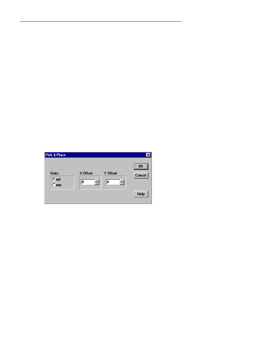
:LQ%RDUG/D\RXW5HIHUHQFH*XLGH
116
.PK?
A separate file is generated for each group of modules. The
?
denotes the sequential number for each report. For example,
for a board file that uses all five of the groups listed above,
Pick & Place generates the following file extensions:
•
.PK1
—This file lists the through hole components.
•
.PK2
—This file lists the SMD components on the component
side.
•
.PK3
—This file lists the SMD components on the solder side.
•
.PK4
—This file lists the adhesives on the component side.
•
.PK5
—This file lists the adhesives on the solder side.
.PIK
This file is a summary report that lists the output files and the
component counts for each file. The
.PIK
file lists the date
the file was created, the version of WinBoard used to create
the file, the name of the file, the names of all the pick and
place files produced for the current board, and component
counts for each file. A sample of the data in
TEST1.PIK
is
shown at the end of this explanation of Pick & Place.
When you click on Pick & Place, the Pick & Place dialog box displays as
shown next :
Figure 2-48.. The Pick & Place dialog box.
Use Units to set the output units to inches or millimeters.
Use X Offset and Y Offset to set offsets for X and Y coordinates. The
default for both X Offset and Y Offset is zero.
Use OK to accept the changes you have made to the Pick & Place dialog
box and to re-display the main WinBoard dialog box.
Use Cancel to exit out of Pick & Place without saving any settings.

&KDSWHU0HQX5HIHUHQFH
117
Use Help to display online help. The Help tool works similarly to online help
in other Windows-based applications.
An example of how to use Pick & Place follows. Assume the following:
•
SMD and through hole components are used
•
The X offset is 3.0
•
The Y offset is 3.0
To run Pick & Place on
TEST1.BRD
, you would follow these steps:
1.
Click on CAM. The CAM pull-down menu displays.
2.
Click on Pick & Place. The Pick & Place dialog box displays.
3.
Select the appropriate settings as described above and click OK. The
Save Pick & Place Report dialog box displays.
4.
Type
TEST1
in the File Name: text entry box and select the appropriate
directory from the Directories: list box.
5.
Click OK. Pick & Place creates these files:
TEST1.PK1
This file contains a list of all the through hole
components.
TEST1.PK2
This file contains a list of all the SMD components.
TEST1.PIK
This file lists the output files and the component counts
for each file. The summary report has a
.PIK
file
extension. This file lists the date the file was created,
the version of WinBoard used to create the file, the
name of the report file, the names of all the pick and
place files produced, and component counts for each
file. A sample of the data in
TEST1.PIK
is shown
below.
TEST1.PIK Example:
Pick & Place generated by WinBoard X1.00-114 Date
Created: 5/30/1994
Components Pick & Place Report File: TEST1.PIK
Through hole components on the component side
File: TEST1.PK1

:LQ%RDUG/D\RXW5HIHUHQFH*XLGH
118
Component Count
.01 1
10UF 1
290 4
HEAD16 1
SMT components on the component side
File: TEST1.PK2
Component Count
7451 1
74LS51 2
74LS76 2
LED 4
SWDIP-4 1
Adhesive locations on the component side
Output for TEST1.PK1
Pick & Place generated by WinBoard X1.00-114 Date
Created: 5/30/1994
Through Holes Components (Component Side) Report
File: TEST1.PK1
C2
.01
1.3500
1.3000
90.00
C1
10UF
1.3500
1.7500
0.00
R1
290
1.0500
0.7980
0.00
R2
290
1.0500
0.9000
0.00
R3
290
1.0500
1.0000
0.00
R4
290
1.0500
1.1000
0.00
JP1 HEAD16
1.7000
1.9500
0.00
Column 1 is the reference. Column 2 is the part value. Column 3 and 4 are
the X and Y locations. Column 5 is the component orientation in degrees.
Output for TEST1.PK2
Pick & Place generated by WinBoard X1.00-114 Date
Created: 5/30/1994

&KDSWHU0HQX5HIHUHQFH
119
SMT Components (Component Side) Report File:
TEST1.PK2
U5
7451
2.2000
1.6000
0.00
U2
74LS51
2.2000
0.9000
0.00
U4
74LS51
2.2000
1.2500
0.00
U1
74LS76
1.6000
1.6000
0.00
U3
74LS76
1.6000
1.0500
0.00
D1
LED
0.8000
0.8000
-90.00
D2
LED
0.7250
0.9000
-90.00
D3
LED
0.7250
1.0000
-90.00
D4
LED
0.8000
1.1000
-90.00
SW1
SWDIP-4
2.2000
1.9500
0.00
Column 1 is the reference. Column 2 is the part value. Column 3 and 4 are
the X and Y locations. Column 5 is the component orientation in degrees.
BOM
Use BOM to read the current board file and generate a Bill of Materials file.
BOM scans the current board file for all modules and sorts them into
different types based on their module values and part values.
The BOM report has a
.BOM
file extension.
When you click on BOM, the Save Bill of Material Report dialog box
displays.
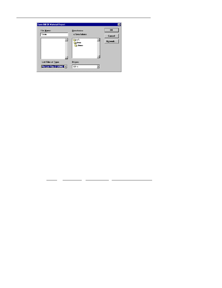
:LQ%RDUG/D\RXW5HIHUHQFH*XLGH
120
Figure 2-49.: Save BOM Report
An example of how to use BOM follows:
1.
Load the board file from which you want to create a Bill of Materials.
2.
Click on CAM. The CAM pull-down menu displays.
3.
Click on BOM. The Save Bill of Material Report dialog box displays.
4.
Type the name you want the Bill of Materials file to have in the File
Name: text entry box and select the appropriate directory from the
Directories: list box.
5.
Click OK. BOM creates a Bill of Materials file with the file name and
directory you specified in step four.
Use Cancel to exit out of BOM without creating any BOM files.
A sample BOM file is shown below.
BOM generated by WinBoard V1.01 Date Created:
4/18/1994
Bill Of Material Report File: test.bom
Count
Component
Module Type Component Reference
1
.01
CK-06
C2
1
10UF
CS13-A
C1
4
290
RC05
R1
R2
R3
R4
1
7451
14SO150
U5
2
74LS51
14SO150
U2
U4
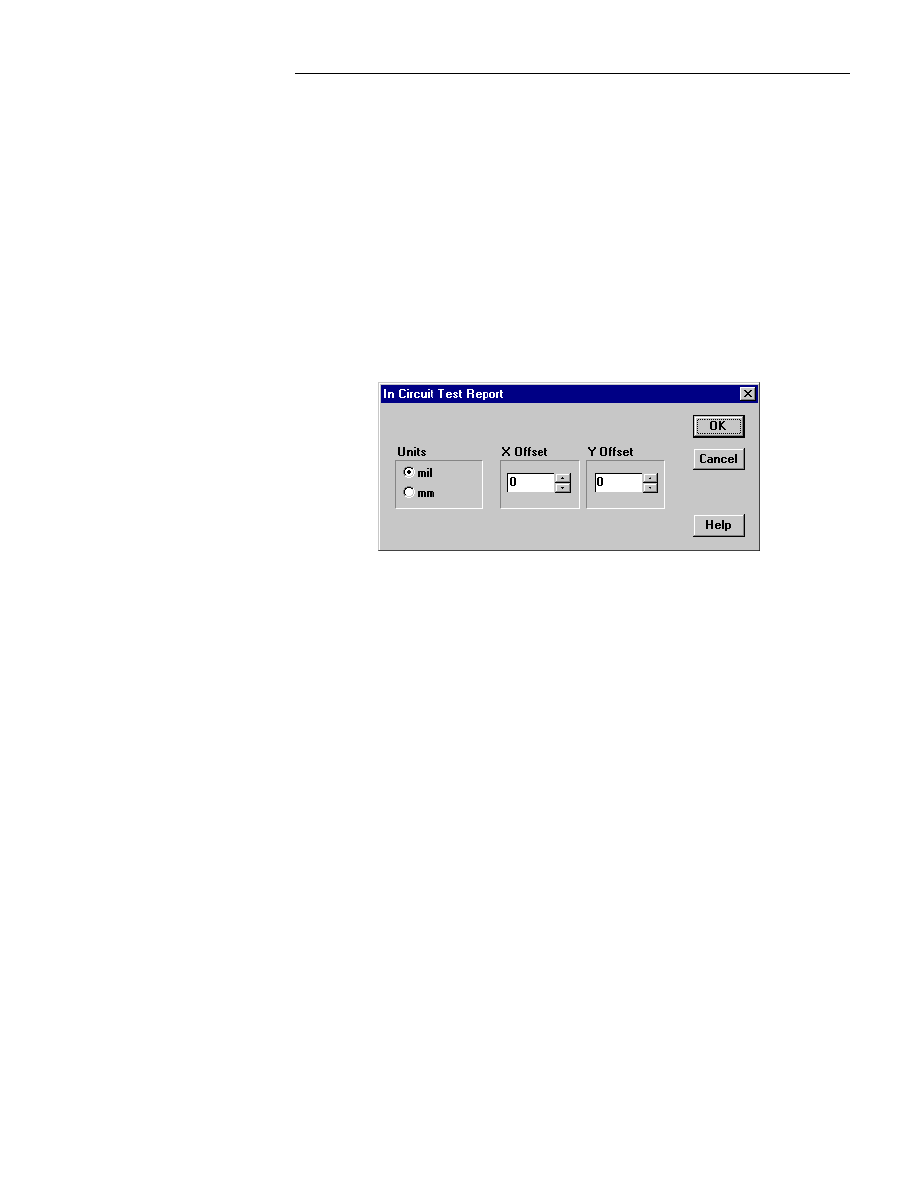
&KDSWHU0HQX5HIHUHQFH
121
2
74LS76
18SO300
U1
U3
1
HEAD16
16HDR-100
JP1
4
LED
P500
D1
D2
D3
D4
1
SWDIP-4
8SO150
SW1
In Circuit Test
In Circuit Test produces the pin and via locations of through and blind vias
only for all nets in the current board file. The two main uses for the In
Circuit Test output are:
1.
To use for producing in-circuit test fixtures.
2.
To give test information to in-circuit test probes.
Figure 2-50.. In Circuit Test Report dialog box.
The In Circuit Test report file has a
.ICT
file extension. The In Circuit
Test report contains the following information listed by column number:
1.
Net name
2.
Either a component reference or the key word
via
3.
Either a pin number—for components, or the via type—
thru
or
blind
4.
The board side the pin or via resides on—
comp
for component side or
sold
for solder side
5.
X location
6.
Y location
Use Units to set the output units to inches or millimeters.

:LQ%RDUG/D\RXW5HIHUHQFH*XLGH
122
Use X Offset and Y Offset to set offsets for X and Y coordinates. The
default for both X Offset and Y Offset is zero.
Use OK to accept the changes you have made to the In Circuit Test dialog
box and to re-display the main WinBoard dialog box.
Use Cancel to exit out of In Circuit Test without saving any settings.
Use Help to display online help. The Help tool works similarly to online help
in other Windows-based applications.
An example of how to use In Circuit Test follows:
1.
Load the board file from which you want to create an In Circuit Test
Report.
2.
Click on CAM. The CAM pull-down menu displays.
3.
Click on In Circuit Test. The In Circuit Test Report dialog box
displays.
4.
Select the appropriate settings as described above and click OK. The
Save In Circuit Test Report dialog box displays.
5.
Type
TEST2.ICT
in the File Name: text entry box and select the
appropriate directory from the Directories: list box.
6.
Click OK. In Circuit Test creates a file similar to the file shown below.
ICTest generated by WinBoard Date Created: 4/18/1994
In-Circuit Test Report File: test2.ict
Net
Mod/Via
Pin/Via
Side
X
Y
A1
U5
2
comp
2.2500
1.6000
A1
U2
2
comp
2.2500
0.9000
A1
via
thru
sold
1.6500
1.8500
A1
via
thru
sold
2.2250
1.7250
A2
U5
3
comp
2.3000
1.6000
GND
U4
7
comp
2.5000
1.2500
GND
via
thru
sold
2.5250
1.2500
GND
via
thru
sold
1.8500
1.4250
VCC
U3
16
comp
1.7000
0.6900
VCC
JP1
15
comp
1.9500
1.9000
VCC
JP1
16
comp
2.0500
1.9000
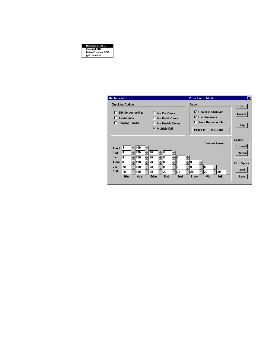
&KDSWHU0HQX5HIHUHQFH
123
DRC
DRC contains the menu selections shown in the DRC pull-down
menu at left. DRC is an acronym for Design Rule Check..
Mechanical DRC
When you click on Mechanical DRC the Mechanical DRC dialog box
displays:
Figure 2-51. : The Mechanical DRC dialog box.
Use the Mechanical DRC dialog box to define the DRC report parameters.
Use Internal Layers and External Layers to specify different parameters
for the internal and external layers of the board.
1.
For each of the Checking Options or Report settings you need to use,
check the box to the left of the option or setting.

:LQ%RDUG/D\RXW5HIHUHQFH*XLGH
124
2. For each of the Checking Options or Report settings you want to
eliminate, remove the check from the box to the left of the option or setting.
Click on Internal Layers, External Layers to select the parameters you
need to set for these layers. The appropriate dialog box displays. The dialog
box for External Layers is shown in Figure 2-27. External layers are the
Solder and Component layers and everything in-between are the internal
layers. A two layer board will not have any internal layers.
The available Checking Options are explained below:
Check Silk Screen on Pads to report all locations where silk screen overlaps
through hole pads, vias, or SMD pads. It is often necessary to remove silk
screen from pads and vias to provide for reliable soldering in manufacturing.
Check T-Junctions to report all T track connections.
Check Hanging Tracks to report unconnected routes.
Check Via on Smd to report any vias overlapping or placed on top of SMD
pads. If holes are drilled in SMD pads, problems could arise when solder
paste soaks into the drill holes. The SMD would not get solidly soldered to
the board in manufacturing.
Check No Via Zones to report any vias placed inside no via zones. This
option is available because it is possible for you to unselect Online
Electrical DRC and place vias inside no via zones.
Check No Metal Zones to report all metal—tracks, pads, and metal zones—
placed inside a no metal zone. This option is available because it is possible
for you to unselect Online Electrical DRC and place metal inside no metal
zones.
Check No Module Zones to report all modules placed inside a no module
zone. This option is available because it is possible for you to unselect
Online Electrical DRC and place modules inside no module zones.
Check Multiple Drill to report any drill holes that are placed directly on top
of each other. Sometimes, during routing, several vias get placed on top of
each other or a via may get placed on top of a pad. Multiple Drill reports
these cases, but only when the drill holes are placed exactly at the same
location.
The available Report settings are explained as follows:

&KDSWHU0HQX5HIHUHQFH
125
Check Report in Clipboard to tell the design rule checker to place a copy of
the report in the clipboard. You can then paste a copy of the report file into
Microsoft WordPad (Write) or Notepad. With this option, you can have both
WinBoard and the error report file on screen simultaneously to help you find
the errors.
Check Use Bookmark to tell the design rule checker to place a book mark on
the board at every location an error is found. Checking this option will also
list all of the DRC errors in the menu
DRC | DRC Error List
.
Mechanical DRC errors are listed as MDRC#, for example MDRC1,
MDRC2, MDRC3. If this option is not checked, then DRC errors will only
report to the clipboard.
Check Save Report in File to tell the design rule checker to save the report
to a file. If you select this option, when you click OK, the standard Windows
Save File dialog box displays for you to specify the file name. We
recommend you use the
.DRC
file name extension.
Use DRC Specs Load to load the template with the DRC settings you need
for a specific manufacturer. When you click on DRC Specs Load, the
standard Windows Load dialog box displays. Select the template file
containing the appropriate settings and click OK. Your DRC settings are
loaded automatically.
Use DRC Specs Save to save DRC settings for future use. Design rule
checking is closely connected to the manufacturing process. Therefore, you
will often have different settings for different processes as well as different
numbers of board layers. WinBoard offers a unique way to save the
manufacturing DRC rules in separate files. Then you can load the template
you need for a specific manufacturer.
When you click on DRC Specs Save, the standard Windows Save dialog box
displays. You can save the template with any name you wish. You will
probably want to use a name that identifies the manufacturer and the process
used. For example:
INHL2LD.TPL
would indicate an in-house 2 layer, low
density board. We recommend you use the
.TPL
file name extension.
Use OK to accept the changes you have made to the Design Rule Checking
dialog box and to run the design rule checker and re-display the main
WinBoard dialog box. If the design rule checker finds any errors, it marks
them with a DRC book mark. For more information about DRC book marks,
refer to
DRC Error List
later in this section.
Use Cancel to exit out of Design Rule Checking without saving any
settings.
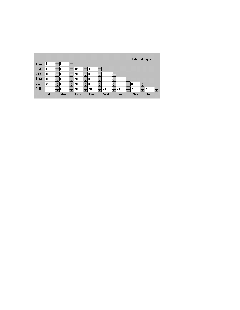
:LQ%RDUG/D\RXW5HIHUHQFH*XLGH
126
Use Help to display online help. The Help tool works similarly to online help
in other Windows-based applications.
The External Layers and Internal Layers dialog boxes look identical
except that one is identified as External Layers, while the other is identified
as Internal Layers. The External Layers dialog box is shown below :
Figure 2-52. Design Rule Checking dialog box for External Layers.
Using the DRC Matrix
The Design Rule Checking matrix is designed to be self-explanatory. To
disable design rule checking on a particular selection, set the option to zero.
Setting items that you do not want to check to zero will also speed up the
checking process.
Definitions of each of the distances are listed in the table below. If nothing
else is specified, the distances are the shortest from the outer edge of the first
object to the outer edge of the other object.
Annular-Min.
The minimum annular ring width for a via.
Annular-Max.
The maximum annular ring width for a via.
Pad-Min.
The overall minimum Pad width.
Pad-Max.
The overall maximum pad width—widest place on
pad stacks.
Pad-Edge
The minimum distance from outer edge of a
through hole pad to the edge.
Pad-Pad
The minimum distance from any through hole pad
to any through hole pad.
Smd-Min.
The minimum width anywhere on an SMD pad.

&KDSWHU0HQX5HIHUHQFH
127
Smd-Max.
The maximum width anywhere on an SMD pad.
Smd-Edge
The minimum distance from any outer edge of an
SMD pad to the edge.
Smd-Pad
The minimum distance allowed from SMD pad to
through hole pad.
Smd-Smd
The minimum distance between any two SMD
pads.
Track-Min.
The minimum track width allowed on the board.
Track-Max.
The maximum track width allowed on the board.
Track-Edge
The minimum distance from any track to any edge.
Track-Pad
The minimum distance from any track to any
through pad.
Track-SMD
The minimum distance from any track to any SMD
pad.
Track-Track
The minimum distance between any two tracks at
any point.
Via-Min.
The minimum via size allowed.
Via-Max.
The maximum via size allowed on the board.
Via-Edge
The minimum distance from any via to any edge.
Via-Pad
The minimum distance from any via to any through
pad.
Via-SMD
The minimum distance from any via to any SMD
pad.
Via-Track
The minimum distance between any via and track.
Via-Via
The minimum distance between two vias on the
board.
Drill-Min.
The minimum drill hole size allowed on the board.
Drill-Max.
The maximum drill hole size allowed on the board.
Drill-Edge
The minimum distance from any drill copper to any
edge.

:LQ%RDUG/D\RXW5HIHUHQFH*XLGH
128
Drill-Pad
The minimum distance from any drill copper to any
through pad.
Drill-SMD
The minimum distance from any drill copper to any
SMD pad.
Drill-Track
The minimum distance between any drill copper
and tracks on the board.
Drill-Via
The minimum distance between drill copper and
any vias on the board.
Drill-Drill
The minimum distance between two drill holes of
any type—via, pad, through hole, or drill hole.
For more detailed explanations of the Design Rule Checking matrix, refer to
Appendix B: DRC Matrix Definitions.
Use OK to accept the changes you have made to the Design Rule Checking
dialog box and to re-display the main WinBoard dialog box.
Use Cancel to exit out of Design Rule Checking without saving any
settings.
Use Help to display online help. The Help tool works similarly to online help
in other Windows-based applications.
Electrical DRC
Electrical Design Rule Check (DRC) is used to check for the electrical
parameters associated with the netlist. These electrical parameters are:
Track Width and Isolation (Track spacing). Selecting this option will open
the following dialog box:
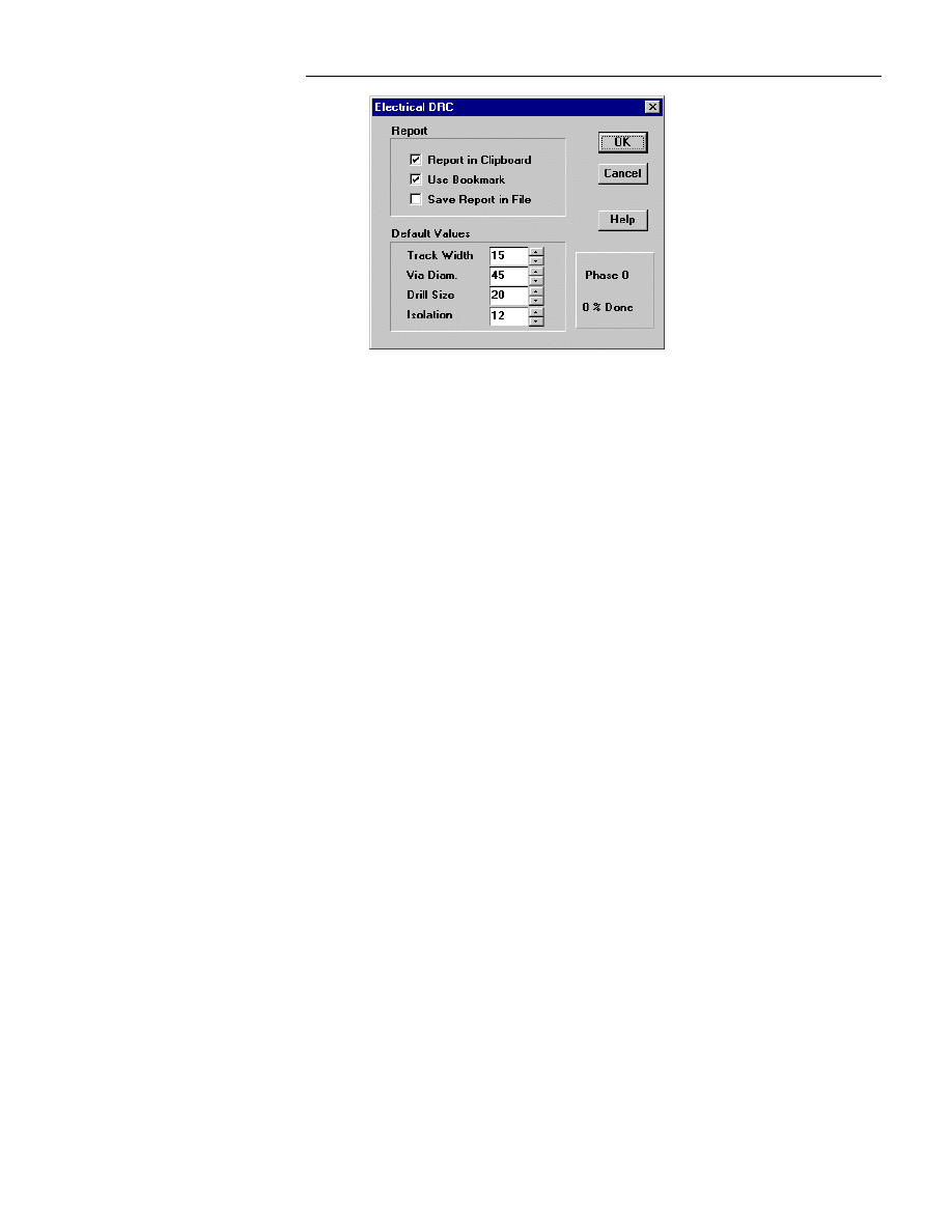
&KDSWHU0HQX5HIHUHQFH
129
Figure 2-53.: Electrical DRC.
Report settings
Check Report in Clipboard to tell the design rule checker to place a copy of
the report in the clipboard. You can then paste a copy of the report file into
Microsoft WordPad (Write) or Notepad. With this option, you can have both
WinBoard and the error report file on screen simultaneously to help you find
the errors.
Check Use Bookmark to tell the design rule checker to place a book mark on
the board at every location an error is found. Checking this option will also
list all of the DRC errors in the menu
DRC | DRC Error List
.
Electrical DRC errors are listed as EDRC#, for example EDRC1, EDRC2,
EDRC3. If this option is not checked, then DRC errors will only report to the
clipboard.
Check Save Report in File to tell the design rule checker to save the report
to a file. If you select this option, when you click OK, the standard Windows
Save File dialog box displays for you to specify the file name. We
recommend you use the
.DRC
file name extension.
Default Values
When you start a board file, you are prompted for the four default settings:
Track Width, Via diameter, Via drill size and Isolation (Track spacing).
These are the board defaults and only apply to nets that do not have specific
net parameters assigned to them.
:LQ%RDUG/D\RXW5HIHUHQFH*XLGH
130
When you run Electrical DRC, it will check for violations for each specific
net according the specified values assigned to that net in the netlist. The
default settings apply to all other nets that do not have values specified in the
netlist.
How it works
1.
In WinDraft Schematics, you use the feature
Place | Net
Properties
and assign net specific properties as follows:
Net Name
Track Width
Track Isolation
GND
20 mils
12
VCC
30 mils
20
Clock
15 mils
12
2.
The above values are now part of the netlist. When you start routing
traces in WinBoard, it will use these net specific values. For all other
nets with no net specific values, it will use the default values you entered
when you started the board, unless these defaults were manually changed
when you routed.
3.
When you run Electrical DRC, it will check GND to make sure it is
according to these net specific parameters. If it is smaller than the
specified setting it will report a violation. For example, if you manually
changed GND while routing and placed traces at 10 mil widths, this will
report as a violation. If the net VCC is closer than 20 mils to another net,
then this will report as a violation.
Electrical DRC will only test for violation according to the netlist, and the
defaults only apply to nets with no net parameters. If you want to test for
violations and do not want to use the values associated with each individual
net, then use the Mechanical DRC described earlier in this section.
If WinBoard uses the net parameters specified in the netlist when you start
routing a trace, then how could an electrical violation occur? If you press the
W key while routing you can change any of the net parameters for a trace. A
net parameter could also be changed in the track dialog box before beginning
the trace. Finally, if On-Line DRC is not on while routing, then there is no
warning when violations are created.

&KDSWHU0HQX5HIHUHQFH
131
Use OK to start Electrical DRC.
Use Cancel to exit the Electrical DRC dialog box without saving any
settings.
Use Help to display on-line help.
The Phase indicators shows the progress of Electrical DRC. There are three
phases, the third will take the longest to run.
On-Line Electrical DRC
Use On-Line Electrical DRC to warn and prevent you from placing objects
that violate net parameters. This will use the values specified for each
individual net in the netlist. If no net parameters are specified in the netlist, it
will use the Default values specified when the board was created and as listed
in the Electrical DRC dialog box.
If a violation would occur while you are placing objects, the system beeps
(using the Error Bell) to indicate that what you are trying to do violates the
Electrical DRC Rules. WinBoard prevents you from creating an Electrical
DRC violation while On-Line Electrical DRC is active. The Error Bell may
be turned on/off in the
Tools | Options
dialog box.
To enable On-Line Electrical DRC select
DRC | On-Line
Electrical DRC.
A check mark on the menu will indicate that the On-
Line DRC is activated.
DRC Error List
Errors from the Mechanical DRC and Electrical DRC both display in the DRC
Error List box. Use
DRC | DRC Error List
to open this box, or click
the icon on the toolbar.
Mechanical errors display as MDRC followed by the error number. For
example MDRC1, MDRC2, MDRC3.
Electrical errors display as EDRC followed by the error number. For
example EDRC1, EDRC2, EDRC3.
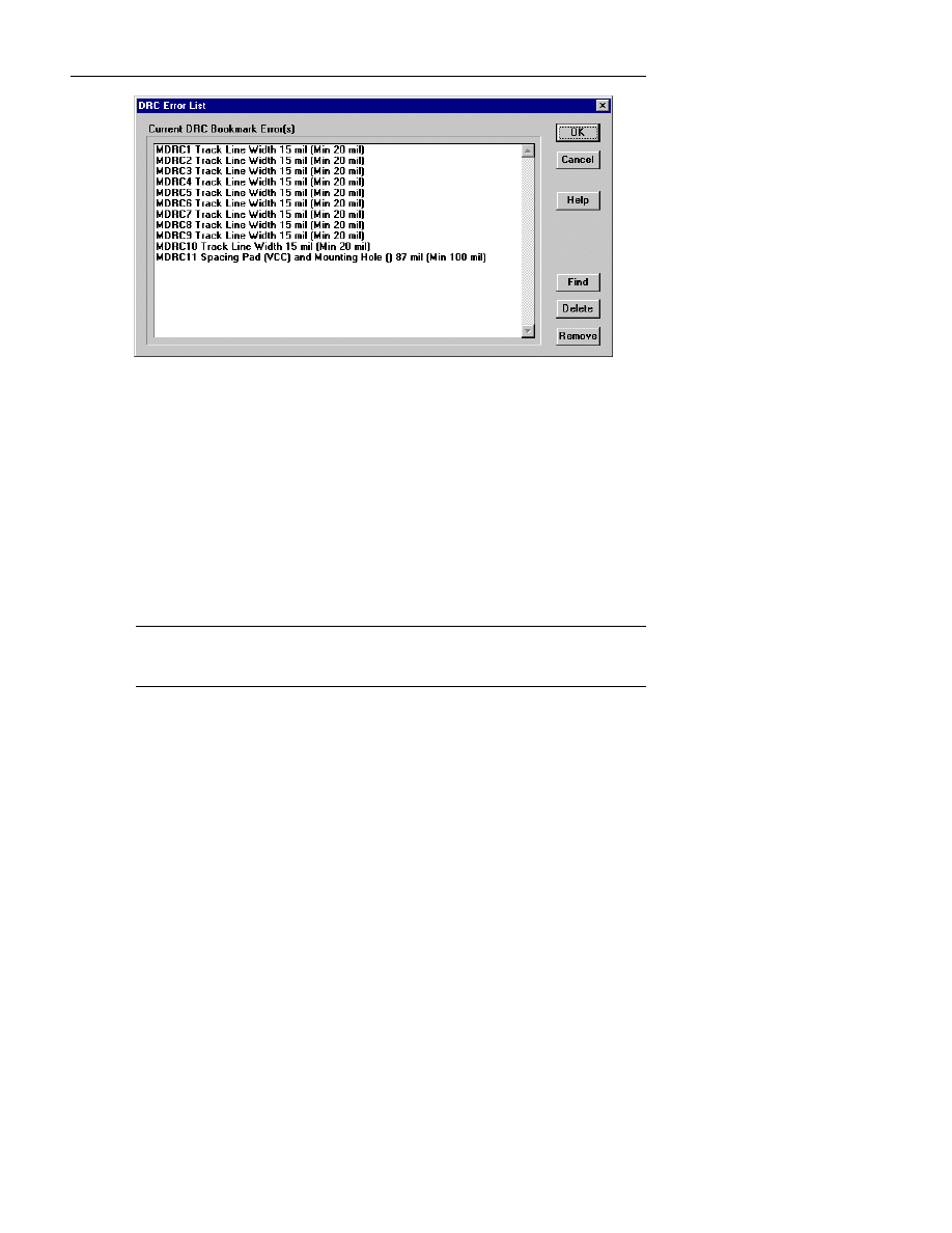
:LQ%RDUG/D\RXW5HIHUHQFH*XLGH
132
Figure 2-54.: DRC Error List.
View DRC Errors
Use the Current DRC Bookmark Error(s) list box to select the error you
want to find. To find an error, double-click on the error in the list box, or
click on the error in the list box and click Find. The pointer will go to the
location of the error on the board.
You can view the violation information for a particular book mark from the
main WinBoard screen. Place the left mouse button on the DRC book mark
and press the F2 key to read the violation information on the status line at the
bottom of the screen.
F
NOTE: When you run DRC, any book marks remaining from before are
automatically deleted by DRC.
Use Cancel to exit the BookMark dialog box without saving any settings.
Use Help to display online help. The Help tool works similarly to online help
in other Windows-based applications.
Use Delete to remove a selected DRC violation from the list. Click on a
violation in the list box to select it, then press the Delete button to remove it
from the list.
Use Remove to delete all DRC violations from the list box and to remove all
DRC error markers from the board.

&KDSWHU0HQX5HIHUHQFH
133
Utilities
Utilities contains the menu selections shown in the Utilities pull-
down menu at left.
Statistics
Statistics gives all of the statistics for the board file, including:
•
The number of pads by type: Through and SMD
•
The number of lines by type: Tracks, outlines, and edges
•
The number of vias by type: Through, blind, and buried
•
The number of objects by type: Adhesive, book marks, dimensions,
mounting holes, pass marks, and targets
•
The number of pieces of text by type: Copper, silk, and component
•
The number of zones by type: Metal, no metal, no via, and no module
•
The computer resources currently being used: Board file size, free
memory, free disk space, and the date and time.
The Modules box lists the modules in the currently loaded board file.
The Nets box lists the nets in the currently loaded board file.
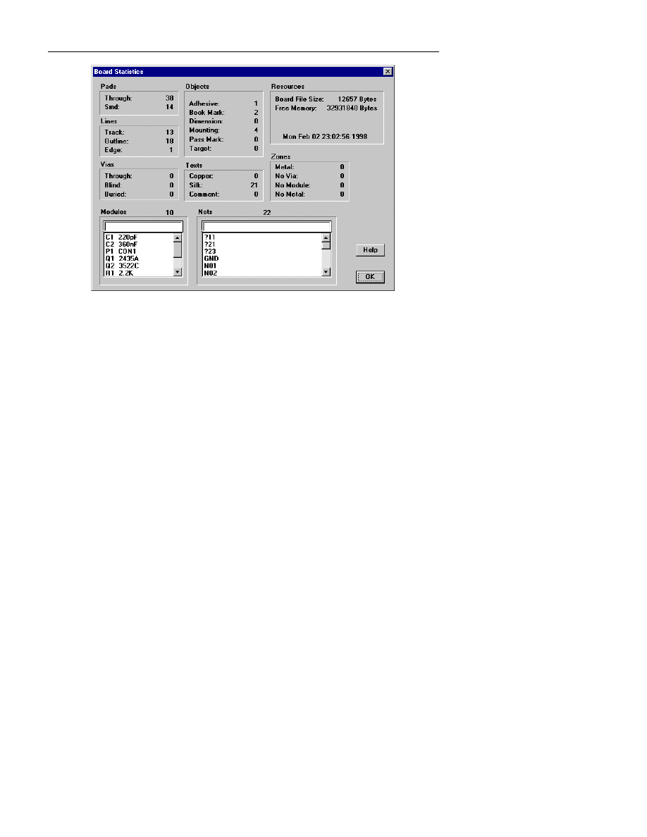
:LQ%RDUG/D\RXW5HIHUHQFH*XLGH
134
Figure 2-55. : The Board Statistics dialog box.
Use Help to display online help. The Help tool works similarly to online help
in other Windows-based applications.
Use OK to exit out of the Statistics dialog box and re-display the main
WinBoard dialog box.
Netlist Report
Netlist Report generates a text file containing all of the netlist information
for the current board.
When you click on Netlist Report, the Generate and Save Board Netlist
dialog box displays as shown next. To generate a netlist report for the current
board, follow these steps:
1.
Select the drive and directory you want the netlist report saved to.
2.
Enter a file name with a file extension of
.NET
.
3.
Click OK. Netlist Report generates a text file and displays the main
WinBoard screen.
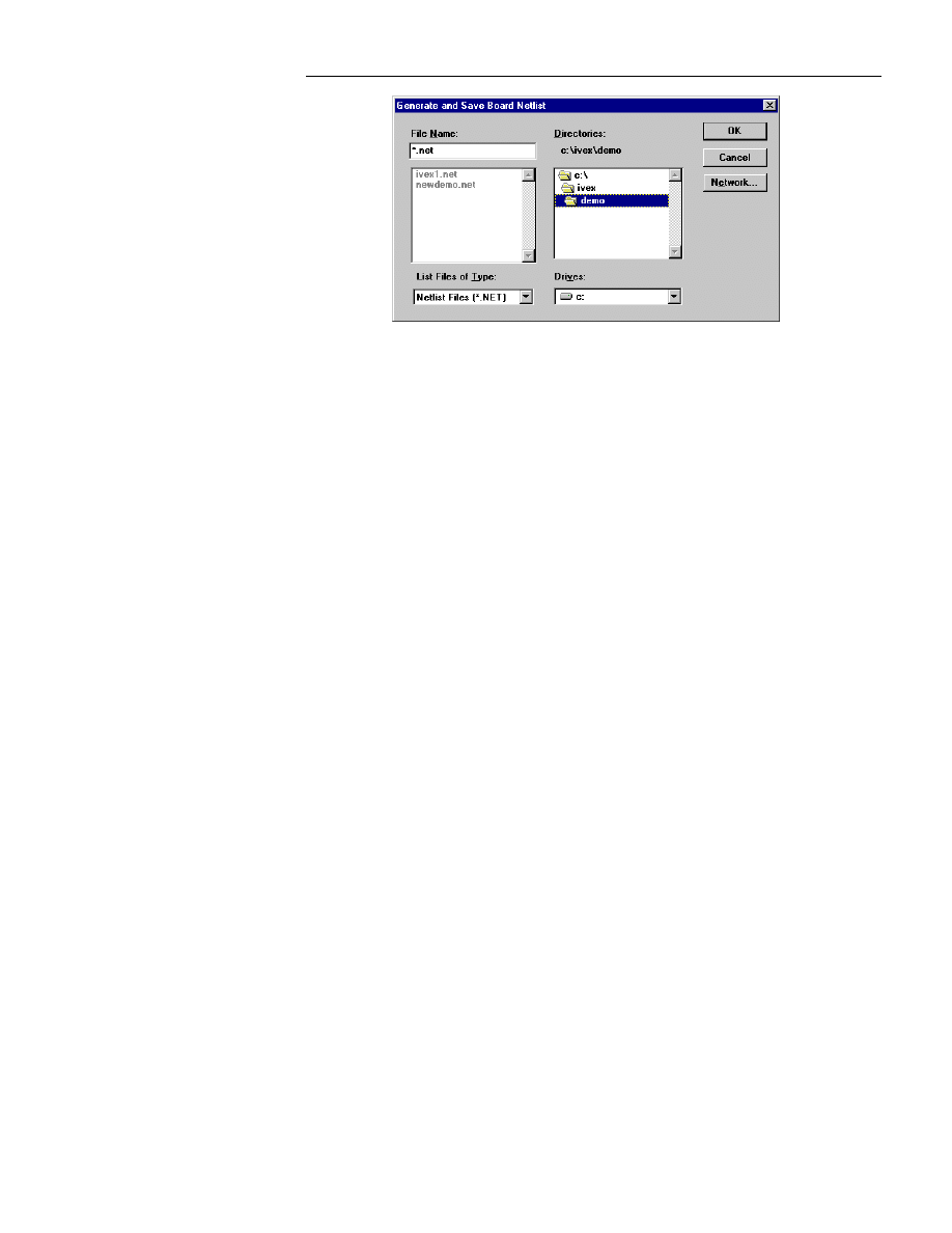
&KDSWHU0HQX5HIHUHQFH
135
Figure 2-56.: The Generate and Save Board Netlist dialog box.
Use Cancel to exit Netlist Report and display the main WinBoard screen
without generating a report file.
Compare Netlists
Compare Netlists compares two WinBoard format netlists and produces a
WAS-IS file and a comparison report.
The WAS-IS file lists the changes to component references, and is used to
read the component reference changes back into the schematic.
The comparison report lists the details of the changes, such as: component
reference changes, nets added or deleted, net changes, and added or deleted
components.
When you click on Compare Netlists, the Old Netlist File Compare dialog
box displays. The Old Netlist File Compare dialog box displays is shown
next:
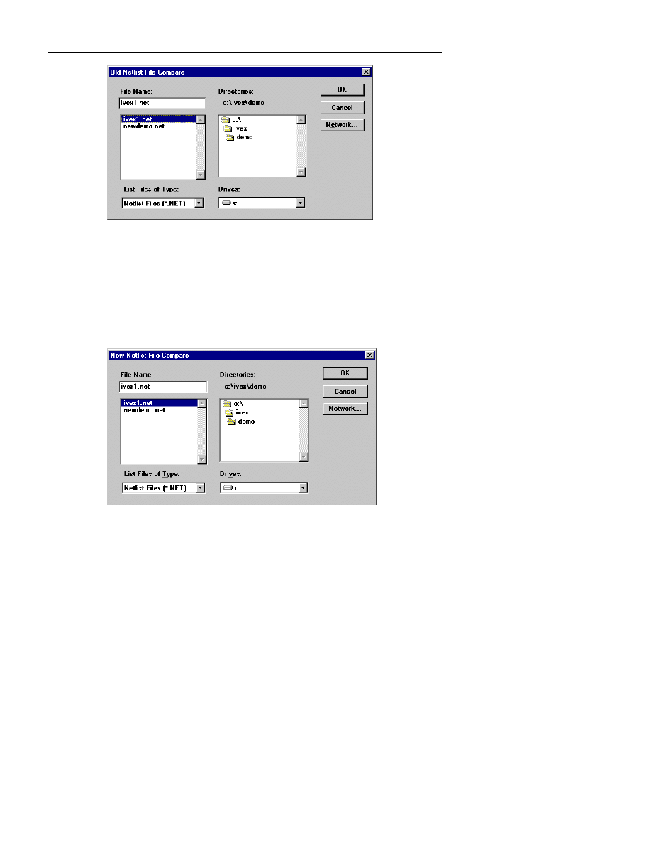
:LQ%RDUG/D\RXW5HIHUHQFH*XLGH
136
Figure 2-57.: The Old Netlist File Compare dialog box.
When the Old Netlist File Compare dialog box displays, follow these steps:
1.
Select the drive and directory on which the first file you want to compare
is located.
2.
Select the first file you want to compare.
3.
Click OK. The New Netlist File Compare dialog box displays as shown
below :
Figure 2-58.: The New Netlist File Compare dialog box.
When the New Netlist File Compare dialog box displays, follow the same
steps as you did with the Old Netlist File Compare dialog box to select a
second file name and click OK.
The Netlist Changes Output File dialog box displays as shown next:
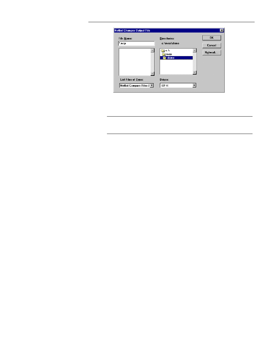
&KDSWHU0HQX5HIHUHQFH
137
Figure 2-59.: The Netlist Changes Output File dialog box.
Follow the same steps as when the Old Netlist File Compare dialog box
displayed, only use a file extension of
.NCP
to save the output file.
F
NOTE: We recommend you use the
.NCP
file extension for all Compare
Netlists report files.
When you click OK, Compare Netlists generates report files similar to the
files shown below.
Example Comparison Report:
Netcomp generated by WinBoard Date Created:
4/18/1994
Netlist Compare Report for CPTEST1.NET and
CPTEST3.NET
R1
Pin: 2 Net: ?2 changed to R1 Pin: 2
Net:
NEWCON
Part: R20
100K is added.
R20
Net: NEWCON is added.
R20
Net: ?102 is added.
WAS_IS File:
R4 R7
Use Cancel to exit out of Compare Netlists without creating the reports.

:LQ%RDUG/D\RXW5HIHUHQFH*XLGH
138
Pin List Report
Pin List Report produces a list of unused pins on the current board and
reports:
•
All pins that do NOT have a net name assigned
•
All pins that have a net name assigned, with only one pin connected to
the net.
When you click on Pin List Report, the Pin List Report dialog box
displays. The Pin List Report dialog box is a standard Windows Save File
dialog box. To create a Pin List Report, follow these steps:
1.
Select the drive, directory, and type of file for which you want to create a
report.
2.
Select the name of the file to which you want the information saved, or
enter a new file name.
F
NOTE: We recommend you use the
.PIN
file extension for all Pin List
Report files.
3.
Click OK. Pin List Report creates a report file similar to the file shown
below.
Unused pin list generated by WinBoard V1.01 Date
Created: 4/18/1994
Unused Pin List Report File: test.pin
U1 8
Net: BUS21B
Stand alone net
U1 15
Net:
No net assigned
U1 16
Net:
No net assigned
U3 15
Net:
No net assigned
U3 16
Net:
No net assigned
In the example report above, U1 pin 8 is an example of a pin with a net name
that only occurs once on the board.
Use Cancel to exit out of Pin List Report without creating the reports.

&KDSWHU0HQX5HIHUHQFH
139
Place File
Place File uses an ascii text file to place modules on the board. You may use
the Place File Report to generate the placement file. This allows you to place
an entire board based on a predetermined placement file.
Create an ascii text file in the following format:
R X Y Side Rotation
Definition:
R: Reference for the Module
X: The X coordinate, measured in inches.
Y: The Y coordinate, measured in inches.
Side: Use Top, or Bottom.
Rotation: A number with 0.01 degree accuracy.
Example:
JP1 X 5.950 Y 1.725 SIDE TOP ROTATION 90
Sample File:
R5 X 2.025 Y 1.600 SIDE TOP ROTATION 0
C3 X 1.350 Y 3.585 SIDE TOP ROTATION 90
R24 X 6.775 Y 5.225 SIDE TOP ROTATION 270
R23 X 6.300 Y 5.275 SIDE TOP ROTATION 0
C15-1 X 8.025 Y 3.800 SIDE TOP ROTATION 0
C15-2 X 8.025 Y 4.050 SIDE TOP ROTATION 0
F
Note: Place File will not move modules with tracks attached.
To use Place File, follow these steps:
1.
Load a netlist and modules are randomly placed on a new board.
2.
Select Place, then Place File. This opens the following dialog box.
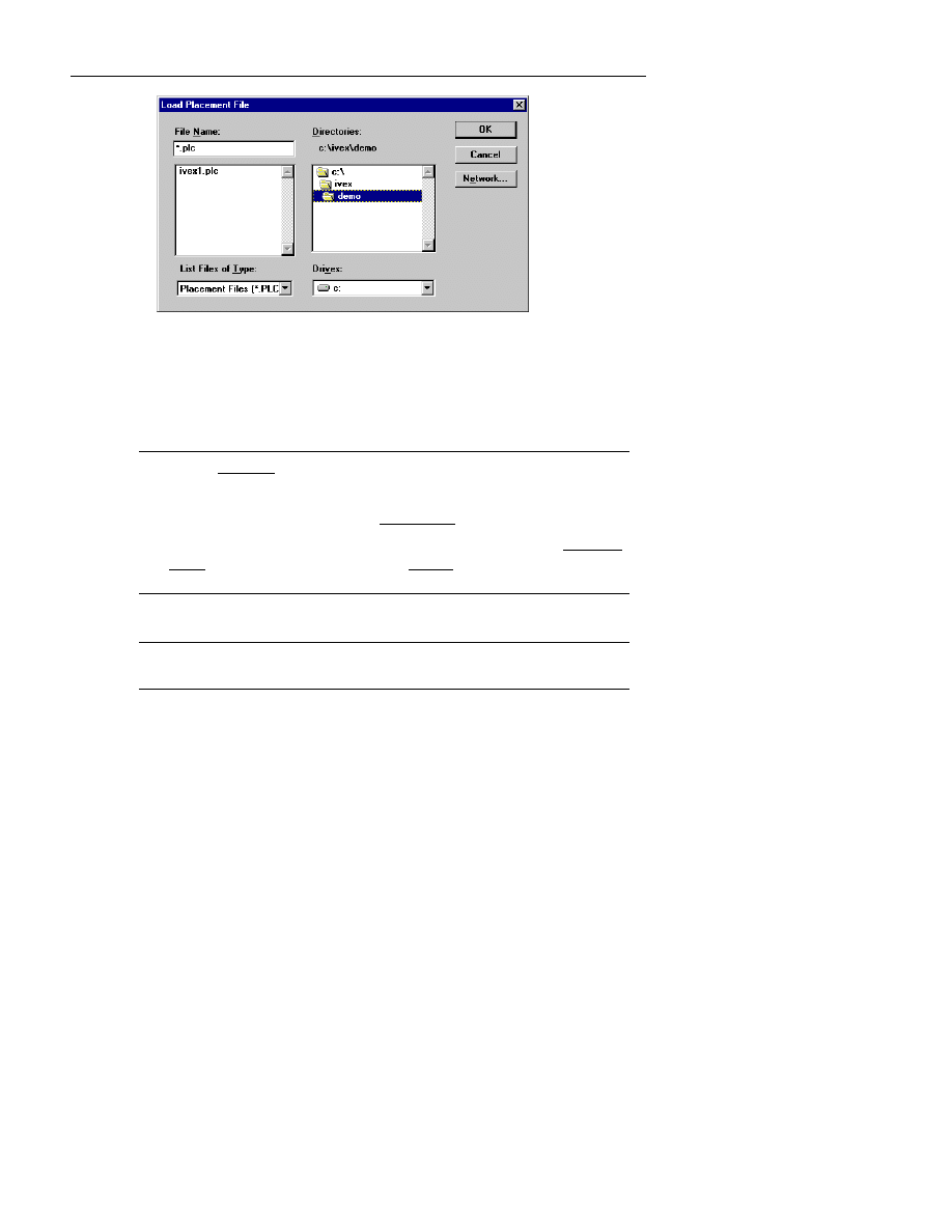
:LQ%RDUG/D\RXW5HIHUHQFH*XLGH
140
Figure 2-60. : The Load Placement File dialog box.
3.
Enter the File Name of the placement file in the Load Placement File
dialog box in the space provided, then press OK.
4.
Modules are placed according to the placement file.
F
NOTE: To speed up placement on larger board (over 100 modules)
follow these steps:
1.
Zoom in on an area with few or no modules.
2.
Now use Place File. This will perform the placement about ten times
faster because the program does not redraw the modules as they are
placed.
F
NOTE: Place file may be used to place any number of chosen modules
on a board.
Place File Report
Use Place File Report to generate a placement file from the current board
file. Use this report to place a board using the Place File function. The Place
File function is extremely useful if you want to replace an existing board with
new modules and use the same X,Y coordinates for placement.
&KDSWHU0HQX5HIHUHQFH
141
For example, generate a placement file using Place File Report. Load the
updated netlist. Then use Place File and select the placement file. In
seconds, the entire board will be replaced using the coordinates of the
placement file.
Renumber Modules
Select Renumber Modules to automatically renumber all Part References on
the board. This will start at the top left corner of the board and renumber the
modules part reference sequentially. Each class of module will start with the
number one, such as R1, R2, R3…and C1, C2, C3…
Use this feature if you have manually placed any parts on the board, added
new parts, or if you have done any manual editing of the part references.
If you have placed new modules, you will first need to assign the default
letter such as R for resistor, C for capacitor, etc. Hold the Ctrl key down and
double click on the module text PART_REF. Change this text to the
appropriate class of module such as U for a dip device. Repeat this for any
other new modules. Now when you run the renumber module feature it will
sequentially add numbers after the appropriate letter.
Window
Window contains the menu selections shown in the Window pull-
down menu at left.
WinBoard is a Multiple Document Interface (MDI) program,
therefore the open boards are listed in the bottom of this menu. You
may select another board file by clicking on the desired board name
in this menu.

:LQ%RDUG/D\RXW5HIHUHQFH*XLGH
142
Help
Help contains the menu selections shown in the Help pull-down menu
at left.
This menu works similarly to the Help pull-down menu in other
Windows-based applications.
Use Key Commands to display keyboard shortcuts, function keys, and other
keyboard commands. This is an extremely useful method to quickly look up
any keyboard commands such as the function keys.
Use X Y Window to display a floating X,Y coordinate box.. This is
especially useful if you use older VGA (640 x 400) display mode that will cut
off the coordinates from the regular toolbar. The bar also displays the pin
capacity of the current window.
Use Registration to enter your personal password registration number.
Refer to the Getting Started Guide for instructions.
Use About to check the current version number and the pin capacity of the
version you are using.
Templates
Templates were designed to simplify the process of repeatedly setting up
board files that use the same tool settings. If you are continuously using the
same tool settings for your board files, all you need do is load the appropriate
template each time you begin a new board file.
Templates are used to save all of the WinBoard tool settings from a particular
board file. After you save a template, you can load the tool settings from that
template into any board file. You can save as many different template files as
you like.

&KDSWHU0HQX5HIHUHQFH
143
Save Template
When you click with the left mouse button on the Save button in the
Template area of any dialog box, the Save Template dialog box displays.
Templates are saved in the program directory and have a
.TPL
file
extension. To save a template, type a template name in the Template Name
text entry box and click OK.
You can also use Save Template in the File pull-down menu to save
templates. Merely click with the left mouse button on Save Template in the
File pull-down menu. When the Save Template dialog box displays, type a
template name in the Template Name text entry box and click OK.
When you save a template, all of the tool settings for the current WinBoard
file are saved to the template file.
The buttons listed below all have a Save button in the Template area of their
dialog boxes:
•
Zone:
Zone templates are zone settings, not actual zones displayed on a
particular board file.
•
Thermal Relief
•
Text
•
Dimensioning
•
Pass Mark
•
Adhesive
•
Target
•
Mounting Hole
•
Track, Outline & Edge
•
Options
Settings are automatically saved with your board file when you save a board
file.
Load Template
To load a template, follow these steps:

:LQ%RDUG/D\RXW5HIHUHQFH*XLGH
144
1.
Click with the left mouse button on Load Template in the File pull-
down menu. The Load Template dialog box displays. Templates are
loaded from the directory in which program files are located and have a
.TPL
file extension. For more information about the location of program
files, refer to Setup in Chapter 2: Menu and Toolbar Reference.
2.
Click in the Template Name list box on the name of the template you
want to load.
3.
Click OK. The template you selected loads into the current board file.
Template settings are loaded for all of the tools listed below:
•
Zone:
Zone templates are zone settings, not actual zones displayed on a
particular board file.
•
Thermal Relief
•
Text
•
Dimensioning
•
Pass Mark
•
Adhesive
•
Target
•
Mounting Hole
•
Track, Outline & Edge
•
Options
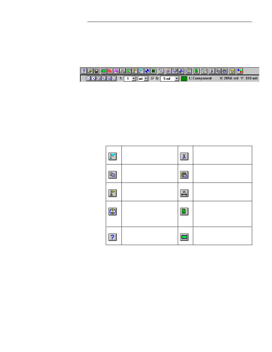
Chapter 3: Toolbars
WinBoard has two toolbars as shown above. The main toolbar runs across the
WinBoard window below the pull-down menus. The secondary toolbar is
below the first, and is composed of buttons used to manipulate the view of
the board file on the computer monitor.
Main Toolbar
The tools are listed in alphabetical order, by tool name in the table below for
a reference. A picture of the button is shown to the left of each button name.
Adhesive
Block Cut
Block Copy
Block Paste
BookMark
Dimensioning
Find & Get
Module
Global Edit
Help
Module
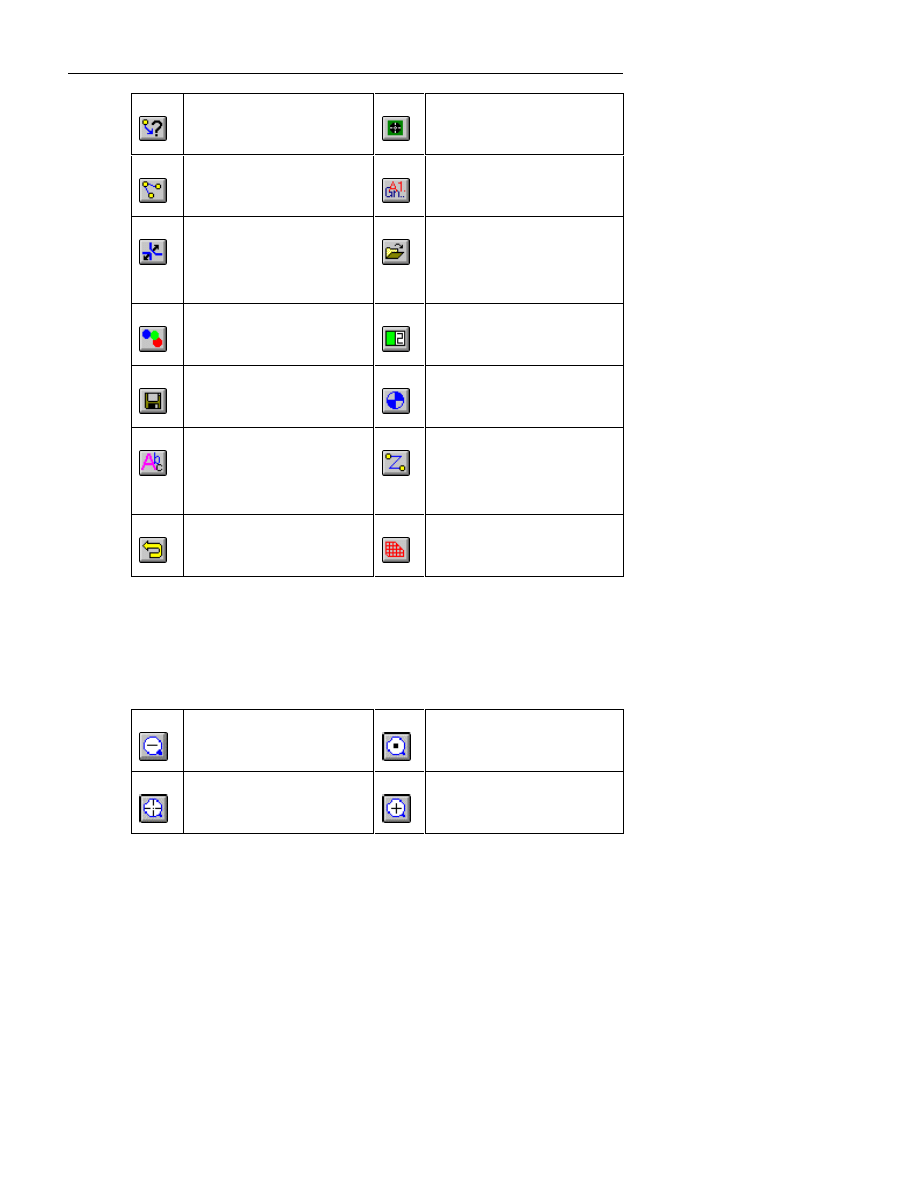
:LQ%RDUG/D\RXW5HIHUHQFH*XLGH
146
More Connections
Mounting Hole
Netlist On the Fly
Nets & Netlist
Online Design
Rule Checking
Open
Options
Pass Mark
Save
Target
Text
Track, Outline &
Edge
Undo
Zone (copper)
Second Toolbar
The tools on the second toolbar are listed in order, by tool name in the table
below. A picture of the button is shown to the left of each button name.
Zoom out
Zoom Center
Refresh Screen
Zoom in
&KDSWHU7RROEDU5HIHUHQFH
147
Zoom Window
Zoom to Fit
For detailed explanations of the WinBoard tools, refer to the tool descriptions
following the table above. In this section, each tool is listed in the order they
appear in the toolbars. A picture of the button is shown to the left of each
button name.
Layer Number Buttons
To the left of the drawing area is a column of buttons containing
numbers. These buttons are the Layer Number buttons. The button for
the layer currently available for editing is white, while all other buttons
are gray.
Click with the left mouse button on the layer number button that matches
the layer you want to edit.
Routing layers (layer pairs)
The Layer buttons are also used to select which ones to toggle through. This
enables you to select only the layers you want active so you may select layer
pairs for routing. By making this selection, the program will only toggle
through the enabled layers when using the V key to place a via.
The program defaults with the top and bottom layers selected (red).
Follow these steps:
1.
Hold down the Shift key on the keyboard and click on the layer
button with the left mouse button.
2.
The layer number will change from black to red, indicating that the
layer is active. Continue to select other layers in this same manner.
Now, when you press the V key the program will toggle through the selected
layers. When you are routing, it will allow you to select layer pairs for
routing, for example:

:LQ%RDUG/D\RXW5HIHUHQFH*XLGH
148
1.
On a six layer board, select layer 1 and layer 2.
2.
Start routing on layer 1 and place a via using the V key.
3.
The program will place a via and switch to layer six without having to
toggle through layers 2-5.
On a layer button that is already red, hold down the Shift key and click on the
layer button to deselect, it will change to black.
F
NOTE: You may also use the + or - keys on the keyboard to change
layers. The +,- keys will toggle through All layers on the board.
Disable layer
To keep a layer from displaying, hold down the
Ctrl
key and click on the
number button with the number of the layer you want to keep from
displaying. If you later want to display a layer for which you have disabled,
simply click once with the left mouse button on the number button with the
number of the layer you want to display.
F
NOTE: Refer to Appendix C: Keyboard Commands for information about all
the other numeric key pad keyboard commands.
Scale and Units
The Scale selection box is shown at left. There a two boxes, one is used
to choose the zoom scale and the other to select the unit (mil, mm, um).
&KDSWHU7RROEDU5HIHUHQFH
149
Scale
The box at left contains the zoom selections available. Click on the arrow
with the left mouse button to open the pull-down box. Then click on the
zoom selection.
Each number represents the number per pixel. For example, if the grid unit
is mils, 2 represents 2 mils per pixel, 50 represents 50 mils per pixel.
You may still use the Home and End keys to zoom in and out respectively.
Units
The Units selection box is shown at left. Click on the arrow with the left
mouse button to open the pull-down box.
Click on the desired unit. The three choices are:
1. mil: mils. One thousandth of an inch.
2. mm: millimeters. One thousandth of a meter.
3. µm: microns. One millionth of a meter, or one thousandth of a
millimeter.
A micron represents one millionth of a meter. The programs internal
database has a resolution of 1 micron.
Grid
The grid (G:) list box located to the right of the scale and units on
the second toolbar is used to set the size of the grid. Use the On Grid
check box located between the S: and G: list boxes to set whether or
not you want objects you place or drag to snap to grid.
:LQ%RDUG/D\RXW5HIHUHQFH*XLGH
150
To change the grid increments, click with the left mouse button on the scroll
arrow to the right of the grid list box. A pull-down list displays. Select the
size by clicking on it.
F
NOTE: To quickly go on or off grid while routing, press the G key on the
keyboard.
The available grid increments are shown in the following table:
Grid Increments:
Mils
Millimeters
Microns
5 mils
1 mm
10
µ
m
10 mils
2 mm
20
µ
m
20 mils
5 mm
50
µ
m
25 mils
10 mm
100
µ
m
50 mils
200
µ
m
100 mils
500
µ
m
1000
µ
m
2000
µ
m
5000
µ
m
Open
Use Open to open a board file that already exists. Available file types are:
Board Files (*.BRD).
Save
Use Save to save a board file in the current project directory. Available file
types are: Board Files (*.BRD).
&KDSWHU7RROEDU5HIHUHQFH
151
Zoom Buttons
Zoom out
Use Zoom out to zoom out to a larger area of the board file. The Home and
End keys on the keyboard may also be used to zoom in and out.
Follow the steps below to zoom out:
1.
Select the Zoom out button. The pointer changes to:
, signifying
that WinBoard has entered the zoom out mode. The view on the screen
pans as you move the pointer.
2.
Place the pointer in the center of the area from which to zoom out, and
click the left mouse button once.
3.
To escape from autopan mode, click the right mouse button once.
Zooming is done in the same increments as those available for scaling the
WinBoard drawing. The table below shows the available zoom and scale
increments:
Mils
Millimeters
µ
m
.5 mil
0.005 mm
.5
µ
m
1 mil
0.01 mm
1
µ
m
2 mils
0.02 mm
2
µ
m
5 mils
0.05 mm
5
µ
m
10 mils
0.1 mm
10
µ
m
20 mils
0.2 mm
20
µ
m
50 mils
0.5 mm
50
µ
m
100 mils
1 mm
100
µ
m
200
µ
m
500
µ
m
:LQ%RDUG/D\RXW5HIHUHQFH*XLGH
152
Center Screen
Use Center Screen to change the center of the view on the screen. Select the
Center Screen button, place the pointer in the center of the area to view, and
click the left mouse button once.
Refresh Screen
Use Refresh Screen to redraw the displayed area of the WinBoard drawing.
The
Z
key on the keyboard performs the same function.
Zoom in
Use Zoom in to zoom in to a smaller area of the board file. The
Home
and
End
keys on the keyboard may also be used to zoom in and out.
Follow the steps below to zoom in:
1.
Select the Zoom in button. The pointer changes to:
, signifying that
WinBoard has entered the zoom in mode. The view on the screen pans as
you move the pointer.
2.
Place the pointer in the center of the area to zoom in on and click the left
mouse button once.
3.
To escape from autopan mode, click the right mouse button once.
Zooming is done in the same increments as those available for scaling the
WinBoard drawing.
Zoom Window
The Zoom Window button shown at left is located on the second toolbar with
the other zoom buttons. The Zoom Window may be used to zoom in on a
specified block and to toggle back and forth between the previous zoom
setting and the zoom window. To use the Zoom Window, follow these steps:

&KDSWHU7RROEDU5HIHUHQFH
153
1.
Define the area you want to zoom. To do this, click on the Zoom
Window button and the cursor changes to a box with an arrow.
2.
Place the cursor at the starting point and click on the worksheet with
your left mouse button, and while holding the button down, drag the
mouse to define an area.
3.
When the area is defined, release the mouse button. This will zoom in on
the block you defined.
4.
Note that the area you defined is still outlined with a dashed yellow line.
Click on a blank area of the screen to remove the zoom window box, or
click on the Zoom to Fit button to toggle back to the previous zoom
level.
Zoom to Fit
Use Zoom to Fit to fit the current board file into the screen.
The Zoom to Fit option also allows you to “toggle” to and from the previous
zoom setting. For example, if you are zoomed in close on a pad while
routing you may want to press the Zoom to Fit button to get a perspective of
the board and where you are going. Press the next zoom button and
WinBoard will automatically toggle to your last zoom setting so that you can
continue routing on your pad at the same setting.


Chapter 4: Using Module
Libraries
Module libraries are files that contain the information WinBoard needs to
display modules in a board file. WinBoard comes with a set of module files.
However, you can add as many custom libraries as you need. WinBoard uses
the
.LIB
file name extension to differentiate module libraries from other
types of files. File names are limited to prefixes with eight characters and
extensions with three characters.
Each library file can contain as many different modules as you like. You will
probably want to group custom modules that have common characteristics in
the same library for easy access.
This chapter explains how to create module libraries.
Creating Modules with the Module Creation
Language
You can create WinBoard modules in a text editor of your choice with the
WinBoard Module Creation Language and compile them with the module
compiler. This section explains how to use the module creation language to
write module source files that enable the module compiler to compile module
source files into module footprints.
WinBoard’s module compiler uses module source files to create module
library files. Library files use the same prefix with different file name
extensions for the module source file and the library file. Library files use the
.LIB
file name extension, while module source files use the
.MOD
file name
extension.
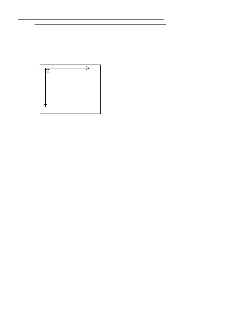
:LQ%RDUG/D\RXW5HIHUHQFH*XLGH
156
F
NOTE: When you use the module creation language to create a module, be
sure to save a copy of your module source file in case you later decide to
make modifications to any of the modules in it.
Before you use the module creation language, you must know how
WinBoard’s coordinate system works. WinBoard’s point of origin (0,0) is at
the top left corner of all WinBoard drawings. See figure 4-1.
+X
+Y
(0,0)
Figure 4-1. WinBoard’s coordinate system
All WinBoard locations are specified with positive (x, y) numbers.
All measurements used in the module creation language, unless otherwise
noted, are real numbers. That is, they may have both an integer part and a
decimal part. The decimal part is optional. WinBoard uses microns as the
default measurement unit. You can also specify millimeters or mils as the
measurement units for modules you create.
Conversions between mils and microns, inches and millimeters, and mils and
millimeters are shown below.
1 mil =
25.4 microns
1 inch =
25.4 millimeters
1 mil =
.0254 millimeter
The anchor point is the point around which the module rotates or turns and
the point from which all other measurements pertaining to the module are
made. The anchor point is usually located at pin one.
Module Creation Language Commands
The module creation language commands are listed and defined
chronologically in this section. In most cases, examples are given after the
&KDSWHU8VLQJ0RGXOH/LEUDULHV
157
command explanation. The module creation language is case insensitive. You
can use uppercase and lowercase letters indiscriminately.
Commands in this section are in uppercase courier type, as follows:
BEGIN
.
The command delimiters that may be used between commands are: commas,
spaces, and. A carriage return terminates a line and denotes the beginning of
the next line.
Comments may be entered by using two slashes (
//
) in front of the
comment. An example of a comment is shown below:
// This is a comment in the module creation language.
UNITS
UNITS
tells the module compiler the kind of units to use for all of the
following modules.
UNITS
may be defined once at the beginning of the source file for the whole
library, or redefined as necessary for each module.
UNITS
may be defined as
MIL
(for mils),
MM
(for millimeters), or
MICRON
(for microns). If no units
are specified, the module compiler uses microns by default.
Examples:
UNITS MIL
Sets the units to mils.
UNITS MM
Sets the units to millimeters.
UNITS MICRON
Sets the units to microns.
BEGIN
BEGIN
marks the beginning of the source code for a given module. The
source code for each module must start with the word
BEGIN
.
PAD STACK
PAD
STACK
gives the compiler the specifications for creating the physical
characteristics of the shapes in a pad stack.
PAD STACK stack_name drill{
shape, orientation, xdim, ydim, xoffset,
yoffset, [layer, layer,
…
, layer]

:LQ%RDUG/D\RXW5HIHUHQFH*XLGH
158
}
PAD STACK
defines the pad stack name, drill size, shape, orientation,
dimensions, location, and layers on which the pad shapes are defined.
Pad stacks enable you to have different characteristics for a single pad on the
top and bottom layer. You can also set the pad shapes on the inner layers to a
smaller size to free up more room for routing.
F
NOTE: You must define all pad stacks before you use
PAD DEF
or
PAD
STEP
commands.
Drill
is the size of the drill hole for the specified pad. If the drill size is 0,
the pad is assumed to be an SMD pad and will be placed on the component
layer. If you later decide to change the layer of the pad, just double click with
the left mouse button on the pad to edit its characteristics.
Shape
is the shape of an entry in the pad stack.
Each pad stack can have a single entry or multiple entries to make up a shape.
This is so that pads can have different shapes and sizes on the component and
solder sides as well as on the inner layers of the board. There are two pad
shapes:
OVAL
(for oval pads) and
RECT
(for rectangular pads).
A pad stack may have as many different entries as necessary to define pad
shapes. For example, you may want a bullet-shaped pad. You need two
entries to define a bullet shape: a rectangle and an oval. See figure 4-2 for an
example of creating a bullet-shaped pad.
Orientation
tells the module compiler how many degrees to rotate the
pad shape.
xdim
and
ydim
are the x and y dimensions of the shape. If
xdim
and
ydim
are equal and the shape is
OVAL
, the shape displays as a circle. If
xdim
and
ydim
are equal and the shape is
RECT
, the shape displays as a square.
x
,
y
is the (x, y) location of the center of the shape with respect to the center
of the pad. To achieve an irregular pad shape, you need to offset one or more
of the shapes. See figure 4-2 for an example of how to create a bullet pad
shape.
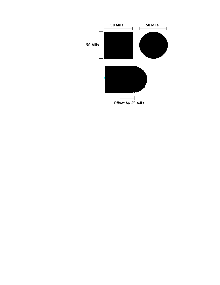
&KDSWHU8VLQJ0RGXOH/LEUDULHV
159
Figure 4-2. Creating a bullet pad shape.
Create the bullet pad shape shown in figure 4-2 by placing a 50 mil square at
the center of the pad and a 50 mil circle offset by 25 mils from the center of
the pad.
Layer
tells the module compiler which layers each pad shape is located on.
The layers must always be inside square brackets[ ] and separated by
commas.
Valid layers for through pads are:
T
For Top layer
I
For Internal layer
B
For Bottom layer
Valid layers for SMD pads are:
C
For Copper
P
For SMD Paste

:LQ%RDUG/D\RXW5HIHUHQFH*XLGH
160
Stack_name
tells the module compiler the name of the pad stack. Stack
names are limited to eight characters.
Example and explanation:
UNITS MIL
PAD STACK bullet 35 {
RECT, 0, 50, 50, 0, 0, [T, I, B]
OVAL, 0, 50, 50, 25, 0, [T, I, B]
}
explanation: Pad stack named "bullet." The bullet has a drill size
of 35 mils and is composed of a 50 mil square located at (0, 0) on
the top, internal, and bottom layers, and a 50 mil circle offset from
the center of the pad horizontally by 25 mils on the top, internal,
and bottom layers.
NAME
NAME
gives the module a name.
NAME
should be the same as the part name on the schematic and in the
netlist. WinBoard uses this name to load the module from the library and
place it into the board file.
Module names are limited to fourteen (14) characters.
Examples:
NAME 14DIP300
NAME TO-5
PAD DEF
PAD DEF
gives the module compiler the specifications for inserting a pad in
the module.
F
NOTE: You must define all pad stacks before using
PAD DEF
commands
.
See
PAD STACK
earlier in this chapter.
PAD DEF, x, y, orientation, stack_name, "padname"

&KDSWHU8VLQJ0RGXOH/LEUDULHV
161
PAD DEF
defines pad stack location, orientation, which pad stack to use,
and the name of the pad being defined.
x
,
y
is the (x, y) location of the pad with respect to the anchor point of the
module.
Orientation
tells the module compiler how many degrees to rotate the
pad.
Stack_name
tells the module compiler which pad stack to use. You must
define the pad stack prior to using it in the
PAD DEF
command. For more
information about defining pad stacks, see the
PAD STACK
section earlier in
this chapter.
Padname
is the name of the pin at the location given in the
PAD DEF
command.
Padname
must be preceded and followed by quotation marks (
"
).
Pad names may have up to four alphanumeric characters.
F
NOTE: The parameters for an existing pad can be copied to a new pad if
the new pad has either an x or y coordinate in common with the previous
pad. This saves you the trouble of repeatedly typing the same information.
This process is called pad stepping. For more information about pad
stepping, see the
PAD STEP
section later in this chapter.
:LQ%RDUG/D\RXW5HIHUHQFH*XLGH
162
Examples and explanations:
UNITS MIL
PAD STACK bullet 35 {
RECT, 0, 50, 50, 0, 0, [T, I, B]
OVAL, 0, 50, 50, 25, 0, [T, I, B]
}
Pad stack
named
"bullet." The
bullet has a
drill size of 35
mils and is
composed of a
50 mil square
located at (0,
0) on the top,
internal, and
bottom layers,
and a 50 mil
circle offset
from the
center of the
pad
horizontally
by 25 mils on
the top,
internal, and
bottom layers.
PAD DEF, 50, 100, 0, BULLET, "1"
Pad 1 at
(50, 100) with
an orientation
of 0, and the
bullet pad
stack shape.
PAD DEF, 100, 100, 0, BULLET, "2"
Pad 2 at
(100, 100)
with an
orientation of
0, and the
bullet pad
stack shape.
PAD STEP
PAD STEP, direction sign distance, "padname"

&KDSWHU8VLQJ0RGXOH/LEUDULHV
163
PAD STEP
tells the module compiler to insert a pad with the same pad
stack, drill size, and orientation as the last pad defined prior to the current
PAD STEP
command, but to change the x or y location of the stepped pad.
PAD STEP
saves you the trouble of repeatedly typing the same information.
You can only use
PAD STEP
for pads that have only the x or y locations
changed. Pads can be stepped one pad at a time. For more information about
the
PAD DEF
command, see the PAD DEF command description earlier in
this chapter.
F
NOTE: If you need to change both the x and y locations, you must use the
PAD DEF
command by itself.
Direction
tells the module compiler whether to step horizontally (in the x
direction) or vertically (in the y direction). The options are
X
or
Y
.
Sign
tells the module compiler whether to step down or to the right (
+
), or
up or to the left (
-
).
Distance
tells the module compiler the distance to step the new pad from
the last pad.
F
NOTE: The direction, sign, and distance must be one contiguous group of
characters. Spaces are NOT allowed between direction, sign, and distance.
Padname
is the name of the pin located at the pad being defined. The
padname must be preceded and followed by quotation marks (
"
). The
padname may have up to four alphanumeric characters.
Example and explanation:
PAD STEP, X+100, "21"
Pad stepped in the x direction +100
units with all of the characteris-tics
of the pad before it, and named "pin
21"
OUTLINE
OUTLINE LINE, x1, y1, x2, y2, layer
OUTLINE BOX, x1, y1, x2, y2, layer
OUTLINE CIRCLE, x1, y1, radius, layer
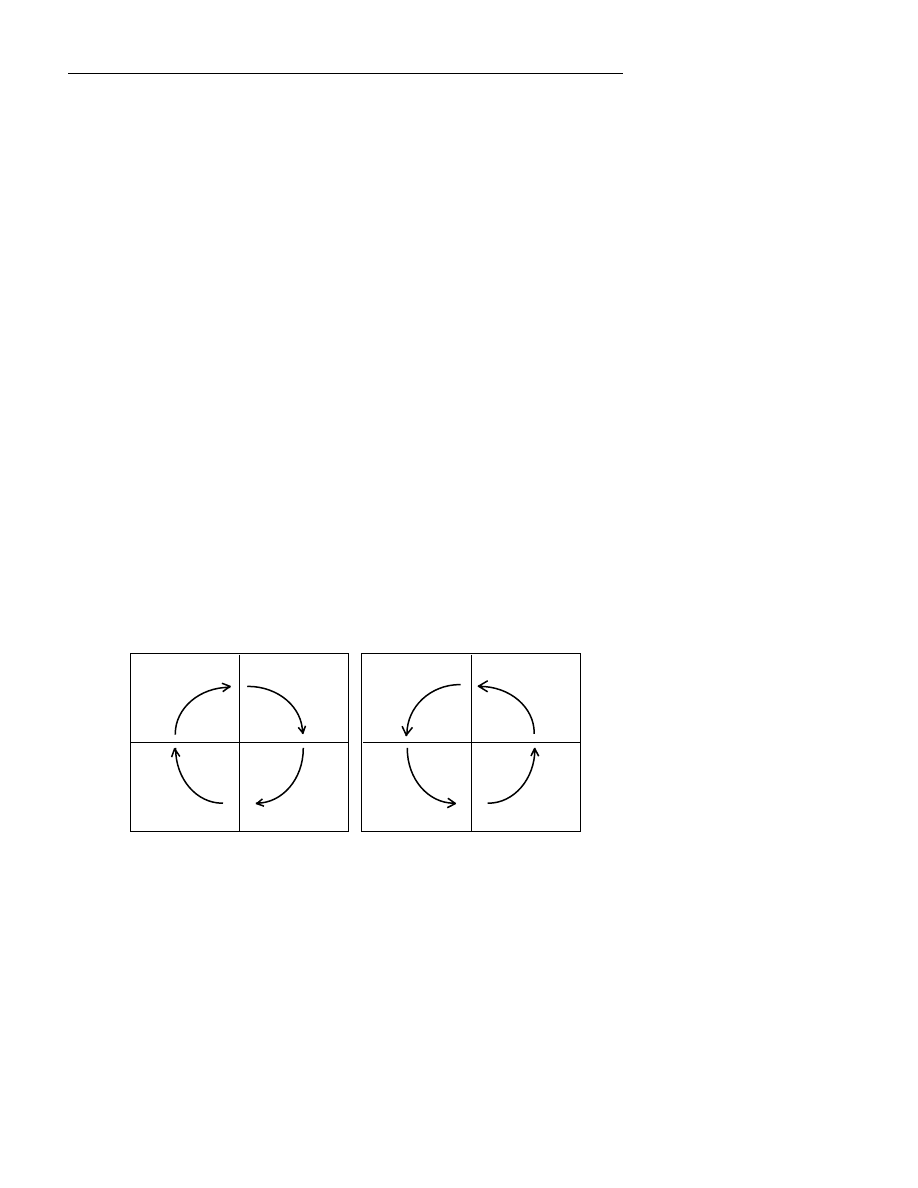
:LQ%RDUG/D\RXW5HIHUHQFH*XLGH
164
OUTLINE ARC, x1, y1, radius, arc_type, layer
OUTLINE
gives the module compiler the specifications for drawing the
module outline.
LINE
tells the module compiler to draw a line from
(x1, y1)
to
(x2,
y2)
.
BOX
tells the module compiler to draw an orthogonal box with opposite
corners at
(x1, y1)
and
(x2, y2)
.
CIRCLE
tells the module compiler to draw a circle with the center at
(x1,
y1)
and a radius specified by the
radius
parameter.
ARC
tells the module compiler to draw an arc with a center point at
(x1,
y1)
and a radius specified by the
radius
parameter. All arcs are drawn as
90 degree arcs.
x1, y1
are coordinates of the start of a line, the first corner of a box, or the
center point of an arc or circle.
x2, y2
are coordinates of the end of a line or the opposite corner of a box.
Radius
is the distance from the center of the circle or arc to the outer edge
of the circle or arc.
Arc_type
tells the module compiler the type of arc to use. There are eight
different types of arcs in WinBoard modules.
The eight types of arcs are shown in figure 4-3.
Type I
Type II
Type III
Type IV
TypeV
TypeVI
Type VII
Type VIII
Figure 4-3. WinBoard’s eight different arc_types.
&KDSWHU8VLQJ0RGXOH/LEUDULHV
165
Layer
is a parameter that specifies which layer, the outline is to be drawn
on. Currently, the only available option is the default
COMP
for the
component layer.
F
NOTE: All (x, y) dimensions are measured from the anchor of the module.
In other words, the point (0, 0) is located at the anchor of the module. All
objects defined with the
OUTLINE
command are placed on the silk screen
layer of the board file.
Examples:
OUTLINE BOX, -100, 50, 800, 250
Box outline with the
first corner at
(-100, 50) and the
second corner at (800,
250). By default, the
outline is drawn on the
component side.
OUTLINE CIRCLE, 50, 0, 200, SOLDER
Circle outline with the
center located at (50,
0) and a radius of 200
units. The outline is
drawn on the solder
side.
OUTLINE ARC, 0,0, 2.3, 1, COMP
Clockwise arc outline
of type one with the
center located at (0, 0)
and a radius of 2.3
units. The outline is
drawn on the
component side.
TEXT
TEXT, x, y, orientation, char_w, char_h, value, layer
TEXT
gives the module compiler the specifications for inserting text in the
module.
x, y
is the (x, y) location of the insertion point of the center of the text
string.
:LQ%RDUG/D\RXW5HIHUHQFH*XLGH
166
Orientation
tells the module compiler how much to rotate the text, in
degrees.
Char_w
is the character width of the text.
Char_h
is the character height of the text.
Value
can be entered as a variable or as a string.
Variable values include
REF
and
VAL
.
REF
and
VAL
act as place holders that
are replaceable by another value later on.
REF
is a place holder for the
reference designator on the module, such as
U2
, for example.
VAL
is a place
holder for the value of the component, such as
74LS00
, for example.
CAUTION: REF and VAL are required to build a module. If you omit
either REF or VAL, the module compiler will flag an error and terminate
compilation of your module source file.
String values may also be included, but must be preceded and followed by a
quotation mark (
"
). Any keyboard character, except quotation marks, can be
used in text strings. An example of a string value is shown below:
"COMMON"
Each text string has an insertion point in the center of the text string. The
insertion point is the point around which the text is rotated if an angle other
than zero is selected.
Examples:
TEXT, 125, -20, 0, 25, 50, REF
Text string with a
reference
designator place
holder, located at
(125, -20) and
characters 25 units
wide by 50 units
high, on the
component side.
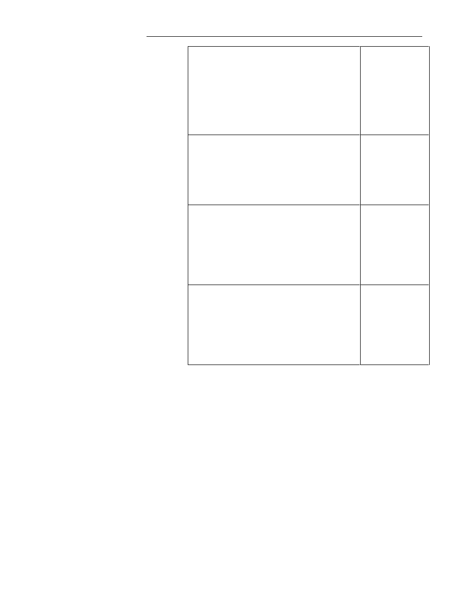
&KDSWHU8VLQJ0RGXOH/LEUDULHV
167
TEXT, 125, 880, 0, 25, 50, VAL
Text string with a
component value
place holder,
located at
(125, 880), and
characters 25 units
wide by 50 units
high, on the
component side.
TEXT, 375, 430, 270, 25, 50, "N.O."
Text string:
N.O.
, located at
(375, 430) and
characters 25 units
wide by 50 units
high, on the
component side.
TEXT, 275, 430, 270, 25, 50, "N.C."
Text string:
N.C.
, located at
(275, 430), rotated
270
°
, and
characters 25 units
wide by 50 units
high, on the
component side.
TEXT, -75, 430, 270, 25, 50, "COMMON"
Text string:
COMMON
, located
at (-75, 430),
rotated 270
°
, and
characters 25 units
wide by 50 units
high, on the
component side.
GRIP
GRIP, x, y
GRIP
gives the module compiler the location of the grip point for PC Board
assembly automatic pick and place machines.
:LQ%RDUG/D\RXW5HIHUHQFH*XLGH
168
x, y
is the (x, y) location of the grip point with respect to the module’s
anchor point for automatic pick and place machines. The default value of
GRIP
is the module’s anchor point (0,0). You only need to define
GRIP
if
you want the automatic pick and place location to be different from the
anchor location.
Example:
GRIP, 50, 25
Automatic pick and place location of (50, 25).
ADHESIVE
ADHESIVE shape, x, y, dimension_w, dimension_h
ADHESIVE
gives the module compiler the shape, location, and dimensions
of an adhesive dot on an SMD component for automatic adhesive machines.
Shape
is the shape of the adhesive dot.
There are two adhesive dot shapes:
RECT
and
DOT
.
x, y
is the (x, y) location of an adhesive dot with respect to the module’s
anchor point for automatic adhesive machines.
Dimension_w
is the width of a rectangular shape.
If the shape is
DOT
,
Dimension_w
is the diameter of the dot shape.
Dimension_h
is the height of a rectangular shape.
If the shape is
DOT
,
Dimension_h
is not necessary.
Example:
ADHESIVE RECT, 0, 0, 25, 100
Automatic adhesive with
rectangular shape, located
at (0, 0), and 25 mils wide
by 100 mils high.
ADHESIVE DOT, 0, 0, 50
Automatic adhesive with
circular shape, located at
(0, 0), and 50 mils in
diameter.
&KDSWHU8VLQJ0RGXOH/LEUDULHV
169
MOUNTING
MOUNTING style, x, y, drill_diameter,
plate_diameter
MOUNTING
gives the module compiler the style, location, drill diameter, and
plating diameter of amounting hole in a component.
Style
is the style of the mounting hole.
There are three mounting hole styles:
SQUARE
,
ROUND
, and
EMPTY
.
SQUARE
, and
ROUND
are plated mounting holes.
EMPTY
is a non-plated
mounting hole.
x, y
is the (x, y) location of a mounting hole with respect to the module’s
anchor point.
Drill_diameter
is the drill diameter.
Plate_diameter
is the diameter of the plated area.
Plate_diameter
applies only to
SQUARE
and
ROUND
holes. If the style is
EMPTY
, it is
unnecessary to define the
Plate_diameter
.
Example:
MOUNTING SQUARE, 0, 0, 35, 50
Mounting hole with square
shape, located at
(0, 0), and 35 mils wide and
a plating diameter of 50
mils.
MOUNTING EMPTY, 0, 0, 35
Empty mounting hole
located at (0, 0), and 35
mils wide
END
END
marks the end of the source code for a given module. All source code
between the
BEGIN
and
END
markers makes up the code for a single
module.
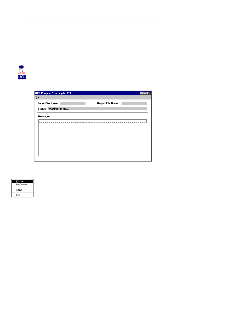
:LQ%RDUG/D\RXW5HIHUHQFH*XLGH
170
Compiling and Decompiling (MCL and Module Libraries)
The Module Creation Language compiler compiles under Windows.
The Module Creation Language in version 2.0 includes a Windows interface
and a function to Compile libraries and Decompile libraries.
Click on the icon at left to open the Module Compiler dialog box. The MCL
icon is located in the Ivex program group. In Windows 95, select Start, press
Programs, then locate the Ivex program group.
Figure 4-4 : The Module Compiler (MCL) dialog box
.
Click on the File menu for the pull-down menu selection shown at left. The
selections are Compile, De-Compile, About, and Exit.
Use Compile to Compile an ASCII MCL source file into an Ivex library file.
The MCL file extension must be the
.MOD
format. This will open a standard
Windows dialog box to select the .mod source file to compile. Press OK to
compile.
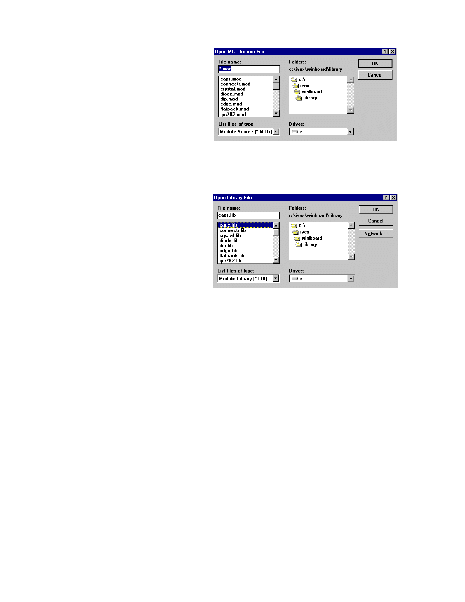
&KDSWHU8VLQJ0RGXOH/LEUDULHV
171
Figure 4-5 : The Open MCL Source File.
Use De-Compile to de-compile an existing Ivex library file into MCL ASCII
format. The extension must be in the
.LIB
format. This will open a standard
Windows dialog box to select the .lib file to de-compile. Press OK.
Figure 4-6 : The Open Library File.
Examples of modules created with the Module Creation
Language
This section shows screen captures of five different modules created using
the module creation language, and the code used to create them. The figure
below shows the 14DIP300 created with the module creation language code
that follows:

:LQ%RDUG/D\RXW5HIHUHQFH*XLGH
172
14DIP300
Figure 4-7. The 14DIP300 created with the module creation language code.
The center of PIN1 is located at anchor point (0,0) .
PIN1 is square.
The code required to construct the 14DIP300 module is shown below:
UNITS MIL
PAD STACK O_55_25 25 {
OVAL, 0.0, 55, 55, 0, 0, [
T, I, B
]
}
PAD STACK R_55_25 25 {
RECT, 0.0, 55, 55, 0, 0, [
T, I, B
]
}
BEGIN
NAME 14DIP300
PAD DEF, 0, 0, 0.0, R_55_25, "1"
PAD DEF, 100, 0, 0.0, O_55_25, "2"
PAD STEP, X+100, "3"
PAD STEP, X+100, "4"
PAD STEP, X+100, "5"
PAD STEP, X+100, "6"
PAD STEP, X+100, "7"
PAD STEP, Y-300, "8"
PAD STEP, X-100, "9"
PAD STEP, X-100, "10"
PAD STEP, X-100, "11"
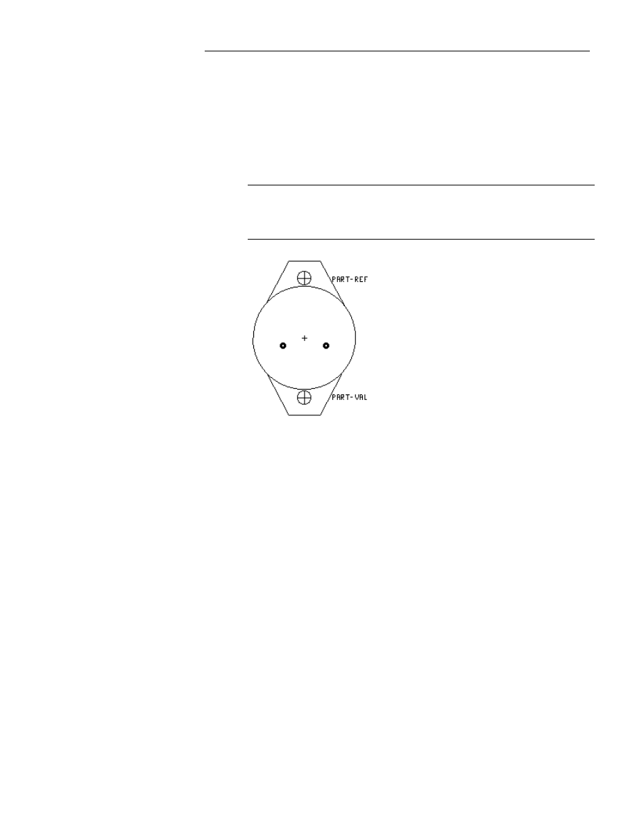
&KDSWHU8VLQJ0RGXOH/LEUDULHV
173
PAD STEP, X-100, "12"
PAD STEP, X-100, "13"
PAD STEP, X-100, "14"
OUTLINE BOX, -50, -250, 650, -50
TEXT, 350, -150, 0.0, 25, 50, VAL
TEXT, -85, -150, -90, 25, 50, REF
END
F
NOTE: For the
PAD STEP
commands above, the previous lines of text can
be copied with your text editor, and the appropriate changes made in the text
to save work.
Figure 4-8. TO-3 created with the module creation language code.
The code required to construct the TO-3 module is shown below:
UNITS MIL
PAD STACK 43_95 43 {
OVAL, 0, 95, 95, 0, 0, [T, I, B]
}
BEGIN
NAME TO-3
PAD DEF, 0, 0, 0, 43_95, "2"
PAD DEF, -440, 0, 0, 43_95, "1"
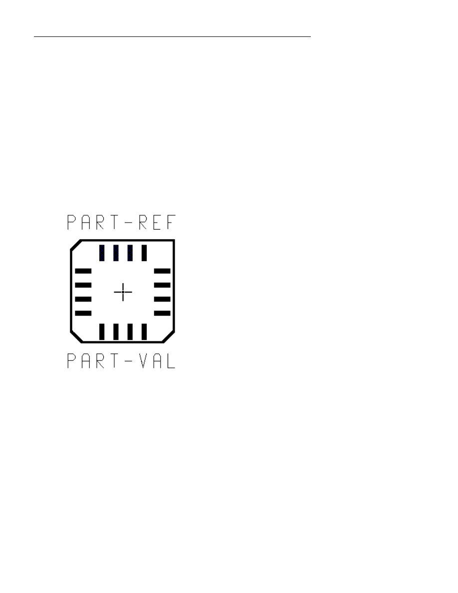
:LQ%RDUG/D\RXW5HIHUHQFH*XLGH
174
MOUNTING ROUND, -220, -685, 151, 171
MOUNTING ROUND, -220, 532, 151, 171
OUTLINE LINE, -381, -863, -59, -863
OUTLINE LINE, -380, 710, -59, 710
OUTLINE CIRCLE, -220, -76.5, 525
OUTLINE LINE, -59, -863, 190.23, -400
OUTLINE LINE, -381, -863, -630.23, -400
OUTLINE LINE, -59, 710, 160.23, 280
OUTLINE LINE, -381, 710, -605, 280
GRIP, -225, -76.5
TEXT, 245, -675, 0, 35, 50, REF
TEXT, 245, 522, 0, 35, 50, VAL
END
Figure 4-9. MO-110AA created with module creation language code.
The code required to construct the MO-110AA module is shown below:

&KDSWHU8VLQJ0RGXOH/LEUDULHV
175
F
NOTE: It is not necessary to declare units because the previous module
declared them as
MIL
.
PAD STACK 20X60 0 {
RECT, 0, 20, 60, 0, 0, [C, P]
}
BEGIN
NAME MO-110AA
PAD DEF, 0, 0, 0, 20x60, "3"
PAD STEP, X+50, "4"
PAD STEP, X+50, "5"
PAD STEP, X+50, "6"
PAD STEP, Y-280, "11"
PAD STEP, X-50, "12"
PAD STEP, X-50, "13"
PAD STEP, X-50, "14"
PAD DEF, -65, -65, 90, 20x60, "2"
PAD STEP, Y-50, "1"
PAD STEP, Y-50, "16"
PAD STEP, Y-50, "15"
PAD STEP, X+280, "10"
PAD STEP, Y+50, "9"
PAD STEP, Y+50, "8"
PAD STEP, Y+50, "7"
OUTLINE LINE, -75, -326, 254, -326
OUTLINE LINE, 254, -326, 254, -4
OUTLINE LINE, 254, -4, 215, 36
OUTLINE LINE, 215, 36, -70, 36
OUTLINE LINE, -70, 36, -110, -4
OUTLINE LINE, -110, -4, -110, -291
OUTLINE LINE, -110, -291, -75, -326
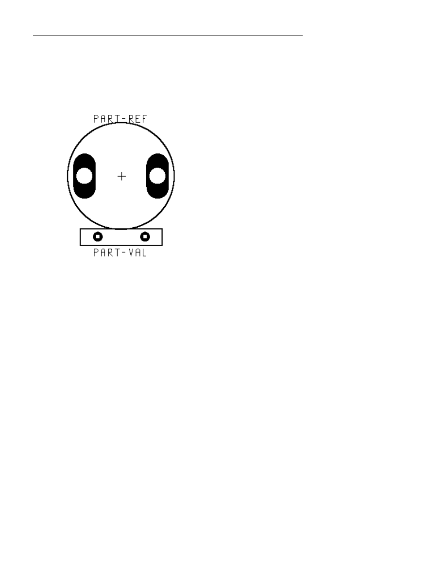
:LQ%RDUG/D\RXW5HIHUHQFH*XLGH
176
GRIP, 72, -145
ADHESIVE DOT, 72, -145, 25
TEXT, 72, -446, 0, 25, 50, REF
TEXT, 72, 156, 0, 25, 50, VAL
END
Figure 4-10. U201 created with the module creation language code.
The code required to construct the U201 module is shown below:
PAD STACK 55_80 55 {
OVAL, 0, 80, 80, 0, 0, [T, I, B]
}
PAD STACK 125_175 125 {
RECT, 0, 175, 175, 0, 0, [T, I, B]
OVAL, 0, 175, 175, 87.5, 0, [T, I, B]
OVAL, 0, 175, 175, -87.5, 0, [T, I, B]
}
BEGIN
NAME U201
PAD DEF, 0, 0, 0, 55_80, "1"
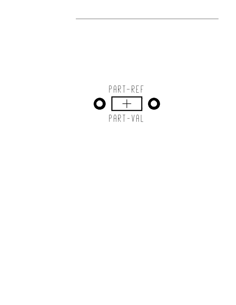
&KDSWHU8VLQJ0RGXOH/LEUDULHV
177
PAD STEP, X+344, "2"
PAD DEF, -94, -437, 90, 125_175, "3"
PAD STEP, X+532, "4"
OUTLINE CIRCLE, 172, -437, 390
OUTLINE BOX, -125, -54, 469, 65
GRIP, 172, -437
TEXT, 172, -857, 0, 20, 25, REF
TEXT, 172, 115, 0, 20, 25, VAL
END
Figure 4-11. CK12-B created with module creation language code.
The code required to construct the CK12-B module is shown below:
PAD STACK CAP_P1 51 {
OVAL, 0, 94, 94, 0, 0, [T, I, B]
}
BEGIN
NAME CK12-B
PAD DEF, 0, 0, 0, cap_p1, "1"
PAD STEP, X+400, "2"
OUTLINE BOX, 90, -50, 310, 50
GRIP, 200, 0
TEXT, 200, -108, 0, 25, 50, REF
TEXT, 200, 108, 0, 25, 50, VAL
END
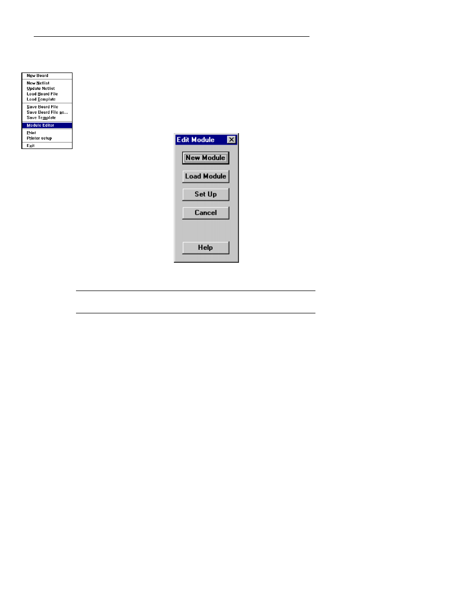
:LQ%RDUG/D\RXW5HIHUHQFH*XLGH
178
Graphical Module Editor
The Graphical Module Editor may be used to create new module footprints,
or to edit existing ones.
To load the editor, select Module Editor in the File menu as shown at left.
This will load the following dialog box:
Figure 4-12 : The Edit Module dialog box
F
NOTE: To specify units, press the Set Up button. Choose Mils, MM, or
Microns.
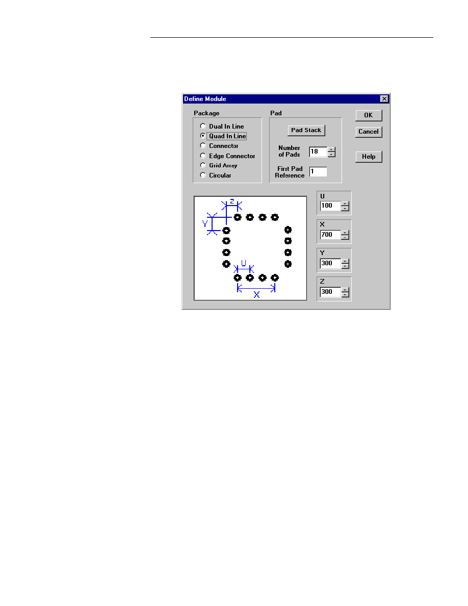
&KDSWHU8VLQJ0RGXOH/LEUDULHV
179
Define New Module
To define a New Module, press the New button in the Edit Module dialog
box. This will load the following dialog box:
Figure 4-13 : The Define Module dialog box.
Package
Define the characteristics of the new module in this dialog box. To select the
type of package click the appropriate radio button. The following Package
selections are available:
•
Dual In Line
•
Quad In Line
•
Connector
•
Edge Connector
•
Grid Array

:LQ%RDUG/D\RXW5HIHUHQFH*XLGH
180
•
Circular
When you select a package, a representation displays in the view box. The
view box also displays pad and module spacing represented by the following
letters:
U
Pad to Pad spacing from the pad center.
X
Control the number of pads in the X direction. This is used to create
an SMD footprint with an unequal number of pads on each side.
Y
Specifies row to row spacing as indicated in the view box.
Z
Specifies row to row spacing as indicated in the view box.
R
Specifies the Radius for a circular package.
Different settings are available for different packages. If a setting is not
available for the package you specified, it will be grayed out in the dialog
box.
Pad
A pad stack must be selected before a new module can be created. To
specify a pad stack, press the Pad Stack button. The following dialog box
will appear:
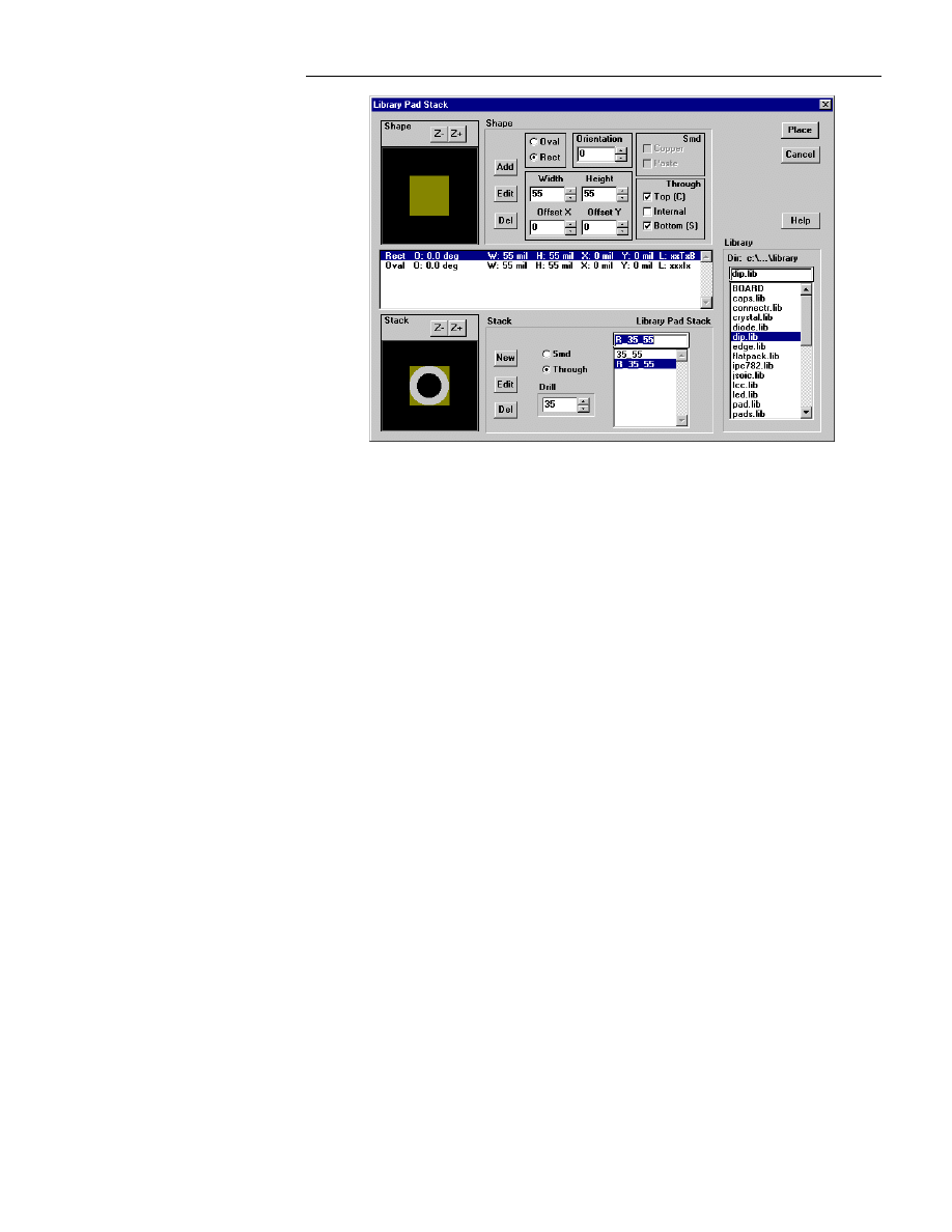
&KDSWHU8VLQJ0RGXOH/LEUDULHV
181
Figure 4-14 : The Library Pad Stack dialog box.
Select or create the desired pad stack in the dialog box. Refer to Chapter 1 :
Editing for more detailed instructions on how to use this dialog box. Press
the Place button to choose the pad stack and return to the Define Module
dialog box.
Number of Pads. Enter the number of pads for the module in this box. This
number may change automatically depending on the values entered for the
pad spacing. Also, for some modules, rounding may occur depending on the
pad spacing values. So check for accuracy before placing the module.
First Pad Reference: Enter the number for the first pad in this box. This is
the Reference pad.
Press OK when all the pad and module parameters have been entered. This
will place the module footprint in the Module Editor work screen. For detail
on how to use the Module Editor refer to the section, Using Module Editor.
Load Library Module
This section describes how to load a module footprint. The module may be
either a new one you just created using the Define New Module dialog box ,
or an existing module that you want to edit.
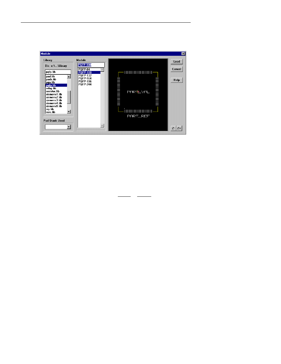
:LQ%RDUG/D\RXW5HIHUHQFH*XLGH
182
To load an existing module, press the Load button in the Edit Module dialog
box. This will load the following dialog box:
Figure 4-15 : The Module dialog box.
Library: Select the library for the module you want to edit. Scroll through
the library names in the list of libraries box, then click on the desired library.
The module associated with the chosen libraries will display in the Module
list box.
Module: Select the Module that you want to edit. Scroll through the list in
the Module list box and click on the desired module. It will display in the
view box. Click on the Z- or Z+ keys to reduce or enlarge the view of the
module.
Load: Press the Load button when you have selected the desired module to
edit. This will load the chosen module and the Module Editor.
Cancel: Press cancel to exit.
Using the Module Editor
The module editor is used for :
1.
Editing an existing module.
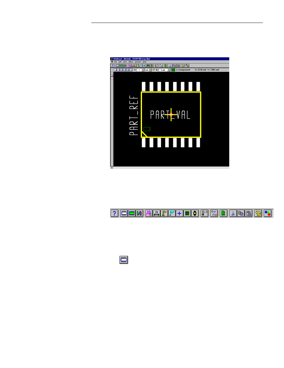
&KDSWHU8VLQJ0RGXOH/LEUDULHV
183
2.
Editing a new module.
When you Load an existing module (see previous section : Load Library
Module), or Create a new module (refer to previous section Define New
Module) the Module Editor screen will appear as follows:
Figure 4-16 :.
The Module Editor screen.
Place the module in the Module Editor workarea as shown above. The
Module Editor screen is different from the regular work-screen and includes
a separate set of toolbar icons.
Figure 4-17 :.
The module editor Toolbar.
Following is a listing of each toolbar icon and a description of how it is used:
Icon
Description:
Create New Module: Click on this icon to load the Define
Module dialog box. Refer to Define New Module earlier in
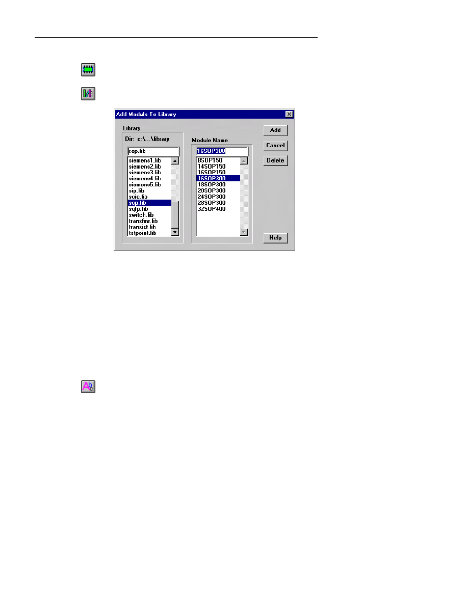
:LQ%RDUG/D\RXW5HIHUHQFH*XLGH
184
this chapter.
Load Module: Click on this icon for the Module dialog box.
Refer to Load Library Module earlier in this chapter.
Write Module File: Click on this icon for the Add Module
to Library dialog box as follows:
Figure 4-18 :
The Add Module to Library dialog box.
1.
In the library section, click on an existing library or enter
the name in the box. The modules associated with the
chosen library will display in the Module list box.
To enter a new library, the
.lib
extension must be used.
2.
Click on the module name to save, or enter a new name in
the box.
3.
Press the Add button to save the module. If the module
already exists it will ask you if you want to replace it.
4.
Press the Delete button to delete a module.
Text: Click on this icon to add text to the module. Use for
Part Reference and Part Value or other text. Text will place
only on the layer where the module is placed. If you want text
on the opposite layer, select or add it after the module is placed
on the board.
&KDSWHU8VLQJ0RGXOH/LEUDULHV
185
Dimensioning: Click on this icon for Dimensioning.
Pass Mark: Click on this icon to place a Pass Mark.
Book Mark: Click on this icon to create or find a Book Mark.
When you create a new module, the program will
automatically add a Reference Book Mark to Pin One. This is
used to determine the Rotation Point and size of the module.
To move the Reference Book Mark, click on it with the left
mouse button to select it. Then move it while holding down
the left mouse button. The Rotation point is usually placed
either on pin one or the center of the module.
The Reference Book Mark is required for a valid module. If
this is moved away from the module, the distance away will
determine the size of the module. If it is removed, the module
will have a very large size which will cause undesirable
results.
Adhesive: Click on this icon to add Adhesive to the module.
Adhesive is used to glue the SMT device to the board. You
may specify either Dot or Rectangle. Adhesive is not required
for a complete SMT module, but it is recommended that you
include this.
Grip Point: Click on this icon to add a Grip Point to the
module. A Grip Point is required for every module. Place this
at the center of an SMT modules and on pin one of through
hole modules. Use only one Grip Point per module!
When you create a new module, the program will
automatically add the Grip Point to the module.
Target: Click on this icon for a Target.
Mounting Hole: Click on this icon for a Mounting Hole.
Create, Place Pad: Click on this icon for the Library Pad
Stack dialog box as shown below:
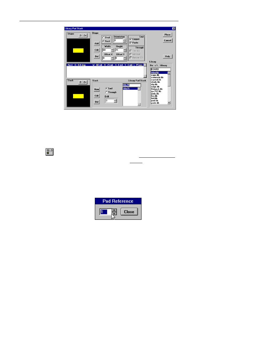
:LQ%RDUG/D\RXW5HIHUHQFH*XLGH
186
Figure 4-19 : The Library Pad Stack dialog box.
Use this dialog box to modify, change, or add pads to the
module you are editing. Refer to the instructions in your Users
Manual for complete details.
Assign Pad Reference: Click on this icon to edit the Pad
Reference of a module. Pin numbers are automatically added
to new modules, this is only used to change the pin reference.
For example:
1.
First, turn on the visible pad numbers in the Tools |
Options | Object Selection dialog box. This way you can
see the number associated with each pad on the module.
2.
Click on the icon at left to load the following dialog box:
Figure 4-20 : Pad Reference.
2.
Enter the alphanumeric pad reference in the space
provided, such as A1.
3.
Place the editor over the reference pin and click with the
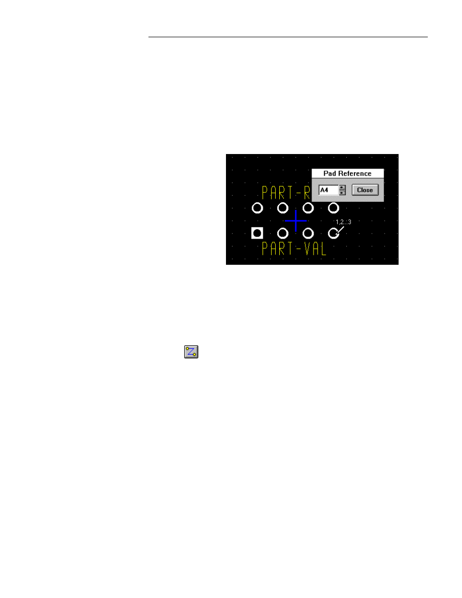
&KDSWHU8VLQJ0RGXOH/LEUDULHV
187
left mouse button. The reference pad has the flag book
mark. If you are uncertain, use the F2 key to identify the
correct pad.
4.
Continue clicking on each pin, it will sequence one
number each time you click on a pad.
5.
Click on the Close button when you are done, this will
close the Pad Reference dialog box.
Figure 4-21 :Editing Pad Reference.
In the example above, we started on the reference pin (square
pin) of the 8 pin connector with A1. The next pin to the right
is A2, then A3, and the editor is currently on A4.
Track, Outline, Edge: Click on this icon to load the Track,
Outline, Edge dialog box as shown below:
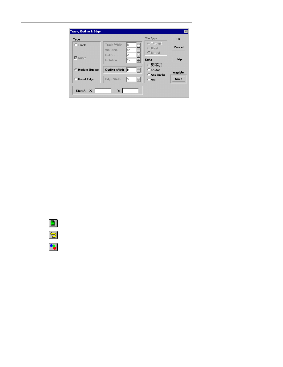
:LQ%RDUG/D\RXW5HIHUHQFH*XLGH
188
Figure 4-22 : Track, Outline & Edge dialog box.
Use the Module Outline function to draw the Module Outline.
1.
Click on the icon shown at left.
2.
In the Track, Outline & Edge dialog box, click on the
Module Outline radio button as shown in the example.
Only the Outline choices are highlighted.
3.
Select the Outline Width in the space provided and click
OK. This will exit the dialog box and place the cursor in
the Track/Outline mode.
4.
Click on the left mouse button for the drawing menu, or
use the keyboard commands B for begin and draw the
outline.
5.
Press N to end and complete the Outline. Press the right
mouse button or esc. to exit the Outline Track mode.
Global Edit: Click on this icon for global edit.
Undo: Click on this icon to undo.
Setup: Click on this icon for the setup dialog boxes. Use to
change color, etc.
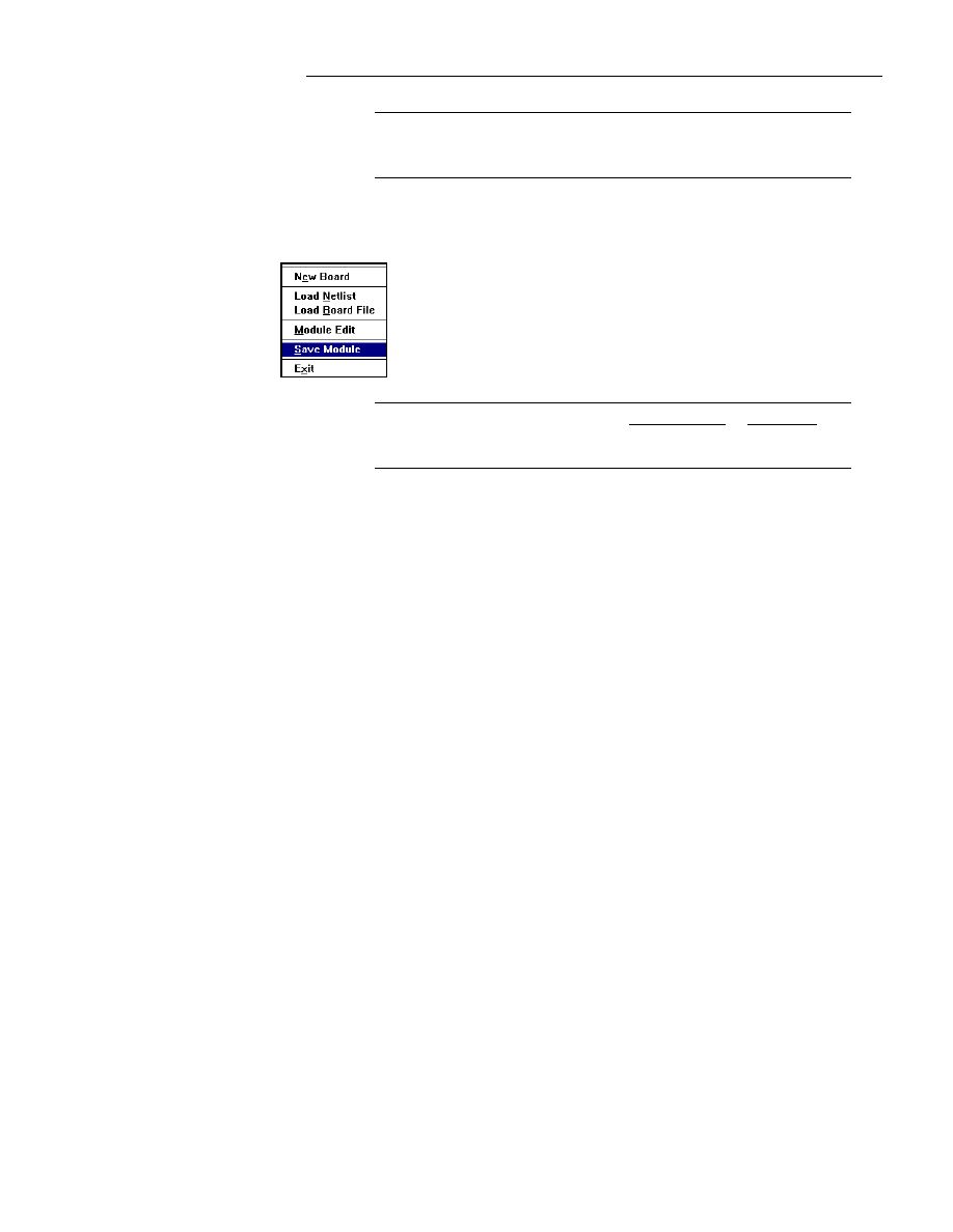
&KDSWHU8VLQJ0RGXOH/LEUDULHV
189
F
Note: The icon description is shown in the Windows status bar located
in the lower left corner of the screen. Hold the cursor over the icon to
view the description.
Saving a module
To save a module, select Save Module from File menu or click on the
Write Module File icon. Enter the name of the library and the module
in the dialog box as described earlier in this section
.
F
Note: If you save a module without a Part Reference or Part Value, the
Text dialog box will open automatically and prompt you accordingly.
Both of these values are required for a valid module.
Before you save a module, be sure that it is correct. Problems could result
from an improperly specified or invalid module. Items to check for include:
•
PART_REF and PART_VAL text names. These must be included and
may not be specified as zero size text objects. If you do not want to view
this text, then turn it off in the Tools | Options dialog box.
•
Reference Book Mark. This is usually on pin one.
•
Grip Point. This is usually on pin one for through hole devises and at the
module center for SMD modules.
•
Pad stack names must be 7 digits in length or less and may not contain
spaces.
•
Library file names must follow file name conventions, i.e.: they must not
contain spaces or be more than 8 characters.
•
Pin and Pad names are usually numbers and not names.
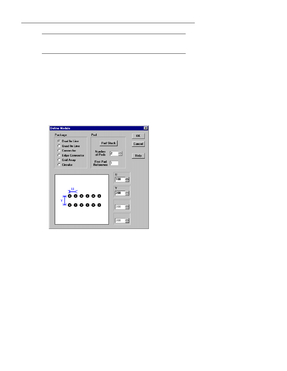
:LQ%RDUG/D\RXW5HIHUHQFH*XLGH
190
F
Note: Be aware of the specifications for the module creation language
(MCL). Objects such as tracks or mounting holes may not compile or
decompile with MCL as they are not part of the MCL specifications. .
Example 1: Capacitor
To create a capacitor, follow these steps:
1.
Load the Module Editor (click on
File | Module Editor
) then
select New.
2.
In the Define Module dialog box, select Dual In Line. The dialog box
displays as follows:
Figure 4-23 : The Define Module box
3.
Press the Pad Stack button. This will open the Library Pad Stack dialog
box. In the Library list, select caps.lib.

&KDSWHU8VLQJ0RGXOH/LEUDULHV
191
4.
In the Library Pad Stack list, click on the existing pad shape 40_75 and
press Place to use this pad shape. (Of course, you could define a new
pad shape with any unique size in this dialog box).
5.
For the Number of Pads enter 2.
6.
For the U and Y values enter U=100 and Y=200. This determines the
spacing for the pads. When creating modules, you will need to refer the
manufacturers data book for these spacing values.
7.
Press OK. You will now see 2 pads spaced 200 mils apart in the
WinBoard Module Editor workarea.
8.
Press the R key on the keyboard (Place | Route) and draw an outline
(box) representing the silkscreen for the module. Draw the outline by
moving and clicking with your mouse.
9.
Select File | Save Module and position the text "PART_VAL". Repeat
this step and position the text "PART_REF". The text Part Ref and Part
Val are required for each module footprint.
10.
Select File | Save Module again and save the capacitor. Enter a library
name such as cap2.lib and enter a part name such as C40.
You now have a new library called cap2.lib and a capacitor module called
C40.
Example 2: Grid Array
To create a Grid Array module, follow these steps:
1.
Load the module editor (click on
File | Module Editor
) then
select New.
2.
In the Define Module dialog box, select Grid Array. The dialog box
displays as follows:
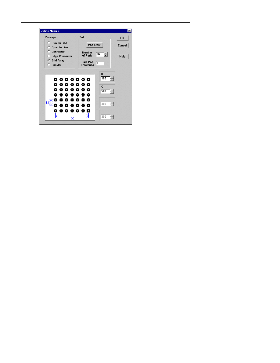
:LQ%RDUG/D\RXW5HIHUHQFH*XLGH
192
Figure 4-24 : Define Module dialog box.
3.
To create a grid array 6 pads by 6 pads with 2 rows of pads, enter 100 for
the pad spacing “U”, 500 for the total module width “X” and enter 36 for
the number of pads.
4.
In this example we will use an existing pad stack. Click on the Pad
Stack button. In the Library section, select dip.lib. In the Library Pad
Stack section, select 25_50. A pad will display in the view box, press
Place.
5.
In the Define Module dialog box, press OK. This will place the module
in the Module editor screen.
6.
Notice that the module is a solid block of pads, 6 rows by 6 columns.
Since you only want two rows of pads, you will need to delete the inner
pads as follows: Hold the
Ctrl
key down while clicking on the 4 pads
in the center. This will select the 4 middle pads. Press the
Delete
key
to remove these 4 pads. The following diagram displays a before and
after example.
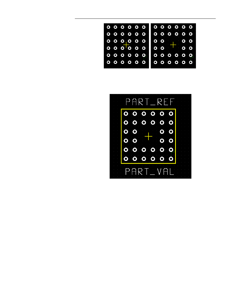
&KDSWHU8VLQJ0RGXOH/LEUDULHV
193
Figure 4-25 : Before and After examples.
7.
You now have a 6 x 6 grid array with 32 total pads. Complete the
module by adding a module outline, press the
r
key to route and draw an
outline similar to the example below:
Figure 4-26 : The completed Grid Array.
8.
Complete the above module by adding the text PART_REF and
PART_VAL. Select
File | Save Module
and it will automatically
prompt for these text values.

:LQ%RDUG/D\RXW5HIHUHQFH*XLGH
194
9.
The third time you select
File | Save Module
, the Add Module to
Library dialog box will open. Select an existing library name or enter a
new name in the format name.lib. Enter the name for the module and
press Add to save it in the specified library file.

Chapter 5: Specctra Interface
This section explains the process and flow of events when using the
WinRoute interface for the application to go from WinBoard to the Specctra
autorouter by Cooper & Chyan Technology (CCT) now owned by Cadence
Design. The Specctra autorouter is an option that is separate from this
program. If you do not have this option and would like to inquire about it,
contact Ivex or your Ivex distributor.
The purpose of the Interface is to translate and convert board files created by
WinBoard into a format that may be used by the Specctra router, then route
the converted board file using Specctra, and finally to return the routed board
file to WinBoard. The Specctra Interface consists of two programs:
1.
Use WinRoute to convert from WinBoard to Specctra.
2.
Use CCT2WB to convert from Specctra to WinBoard.
F
NOTE: WinBoard is known as WinBoard PCB throughout the world except
for Germany where it is known as Ivex PCB. The abbreviation WB refers to
WinBoard PCB and Ivex PCB.
How it works
The WinBoard file is translated into a Specctra file which describes the
physical layout, and a "DO" file (*.DO), that tells the Specctra router how to
handle the routing, number of routing passes, cleanup passes, etc. The
following diagram shows the flow of events from WinBoard to Specctra and
back to WinBoard:
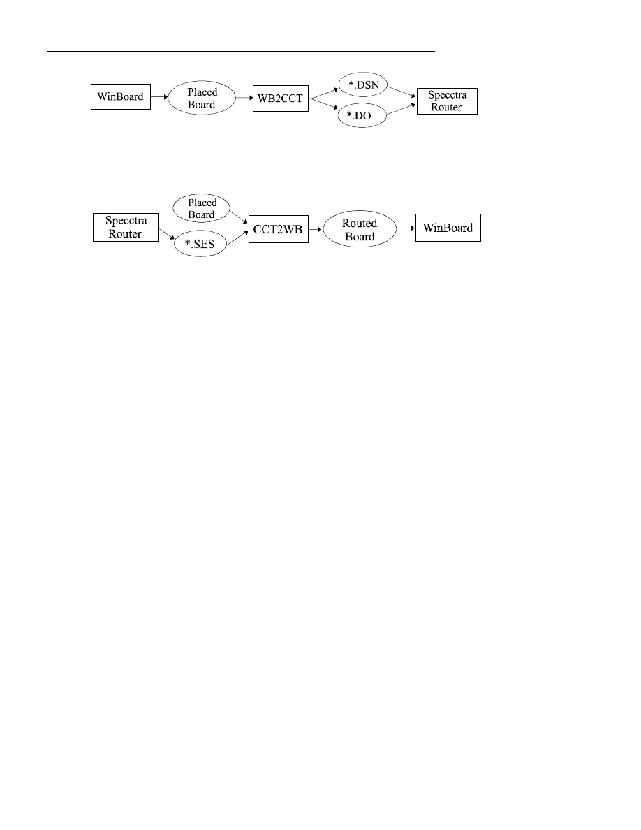
:LQ%RDUG/D\RXW5HIHUHQFH*XLGH
196
The flow in routing a board from WinBoard to Specctra.
The flow of returning the routed board to WinBoard.
The WinRoute (WB2CCT) translates the WinBoard file into a Specctra file
which contains module descriptions, module placement, existing tracks,
power zones, keep out areas, etc. The WB2CCT interface also has the option
to generate a "DO" file, which controls the routing and automatically
launches the Specctra router.
CCT2WB reads the routed track information from the session files generated
by Specctra. They are then merged with the original board file (non or
partially routed), and written to a new WinBoard file. The original board is
kept untouched, so you can reroute the board in case you want to run
Specctra with different parameters. As a safety feature, CCT2WB will not
allow you to overwrite the original file with the merged route file.
Using the Interface
Before you start, you first must save a board file with the modules placed at
the desired locations in WinBoard and it must also have a contiguous board
edge. Refer to the WinBoard Reference manual for specific information.
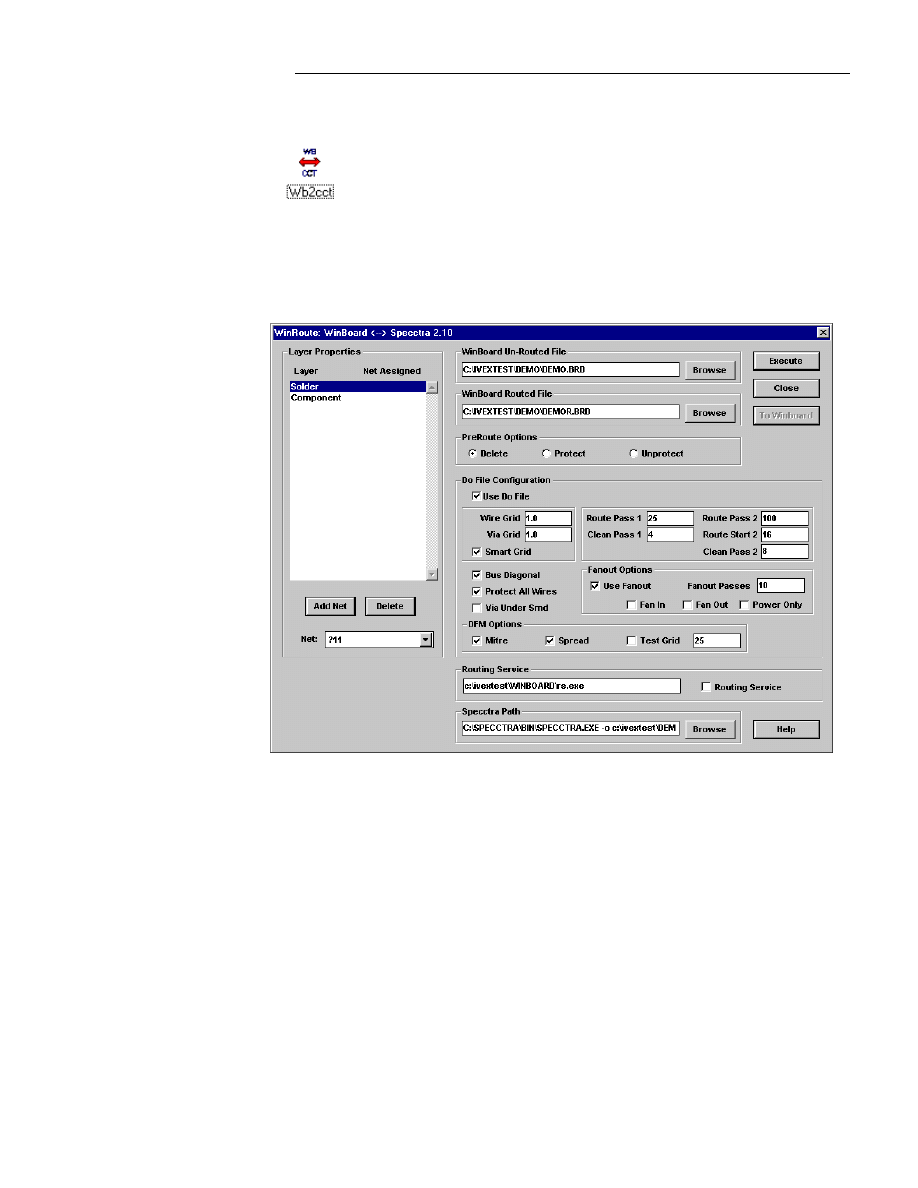
&KDSWHU6SHFFWUD,QWHUIDFH
197
WinBoard to Specctra
The Specctra Interface may be launched manually or automatically
from within WinBoard. To launch it manually, in the Ivex Program
Group, click on the WinBoard to Specctra icon shown at left.
To launch the Interface from within WinBoard, first open your
board file that contains your pre-placed modules and any pre-routed
connections. From the WinBoard menu select Tools | Autoroute.
This will load the interface and the following dialog box will appear:
Figure 5.1 : The WinRoute dialog box

:LQ%RDUG/D\RXW5HIHUHQFH*XLGH
198
How to use the interface:
1.
If you launched the Interface manually, enter the name of the
WinBoard placed board file in the space provided (WinBoard Un-
Routed File). Use the Browse function to assist finding the correct
file and path.
If you launched the Interface from WinBoard, the name of the un-
routed board file is automatically placed in the correct field.
2.
Enter the name you want to use for the routed board file in the space
provided (WinBoard Routed File). Use the Browse function to
assist finding the directory and path.
3.
Enter the desired PreRoute Options. The three radio buttons options
are Delete, Protect, or Unprotect (these are explained later in this
section).
4.
Check Use Do File and enter the settings you want to use for the Do
File Configuration. For most uses the default settings should work
fine. For more details on these options, see Do File Configuration
later in this section.
5.
Click on the Execute button when you have entered your
configurations and are ready to run Specctra and route the board. If
the Use Do File box is checked, the Interface will automatically
launch Specctra and start routing the selected board file.
General Configuration
There are four General Configuration settings: Wire Width, Wire Isolation,
Via Size and Via Drill Size. These settings are taken from your netlist
parameters you previously set in WinBoard.
If you set the net GND to route at a certain track width, then this is what
Specctra will use to route. If you did not set any specific net parameters, then
Specctra will use the default values from WinBoard. The default values are
listed in the EDRC dialog box (DRC | Electrical DRC) and the Track,
Outline, Edge dialog box (Place | Route).
If these are not the defaults you want to use to route your board file, then now
would be a good time to go back to WinBoard and enter in the correct
defaults and then save your board file.
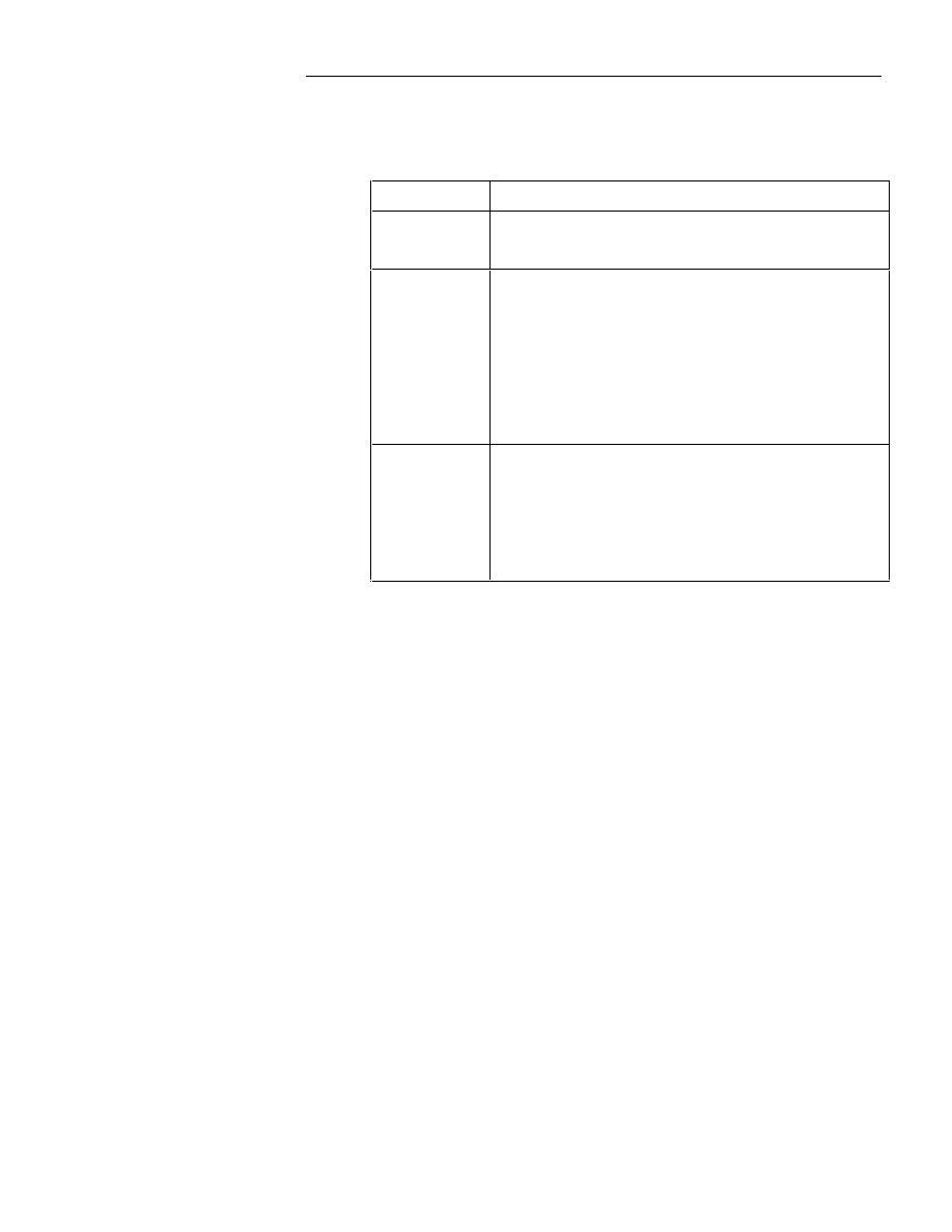
&KDSWHU6SHFFWUD,QWHUIDFH
199
PreRoute Options
Enter the desired PreRoute Options. The three radio buttons options are as
follows:
Option
Explanation
Delete
Removes all existing tracks before transferring the
design to the Specctra router.
Protect
Locks the routes on the board that you have already
placed. e.g. if you pre-routed the GND and VCC
nets, you can prevent Specctra from changing them
by enabling this option.
Please be aware that the over-use of protected tracks
may prevent the autorouter from reaching an
acceptable solution. It is best to preroute only
critical nets, then let Specctra finish the job.
Unprotect
Leaves the tracks that you have already routed, but
not protect them from being moved by Specctra.
In practice, unless you select “Protect”, all of your
tracks will probably be revised by Specctra.
Therefore, the most useful options are Delete and
Protect.
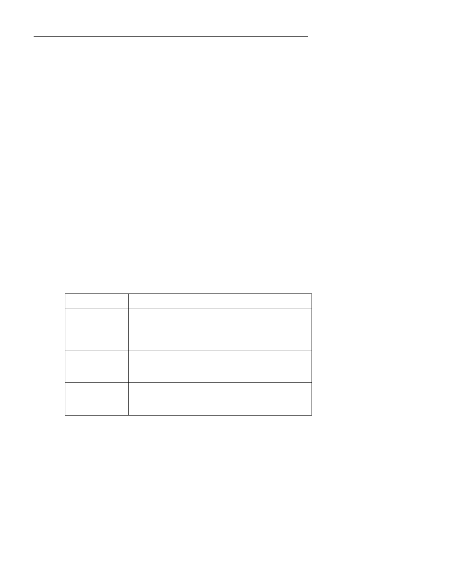
:LQ%RDUG/D\RXW5HIHUHQFH*XLGH
200
Do File Configuration
Check the box next to Use Do File to use the Do File Configuration options.
This will also automatically launch the Specctra autorouter and return when
the Specctra is finished. We suggest you start by using this option. If you
choose to not use the Do File option, then you will need to manually launch
Specctra and make the configuration settings within Specctra.
Set the Specctra Path in the space provided. The Ivex installation
automatically sets the default Specctra path to
c:\specctra\bin\specctra.exe -o error.txt.
You must
set this path location for the Do File to work and automatically launch
Specctra. Once you make the path setting, the Interface will save it.
The setting “-o error.txt” is optional and is used to automatically generate an
ASCII error file. Specctra may not start routing the board file if it finds
serious problems in the board file. These problems could include: no board
edge, duplicate or missing reference designators, duplicate pin numbers, etc.
If you use this option and Specctra does not start routing, then look for the
error file. Load the file into an ASCII text editor. The errors are identified
by “line number”, look at the appropriate line using your text editor. Once
you locate the error description, go back to the original board file and correct
the error.
The following table has definitions for the Do File Configuration settings:
Option
Explanation
Use DO File
If you enable this option, WB2CCT will create a
DO file with the options listed below, and
automatically launch Specctra when you click on
Execute.
Wire Grid
Specifies the routing grid for tracks. Specified in
mils, with one decimal point accuracy. The
default setting is 1 mil.
Via Grid
Specifies the via grid on which Specctra will place
vias. The default is 1 mil, and should be set to
that when you use the
Smart option.
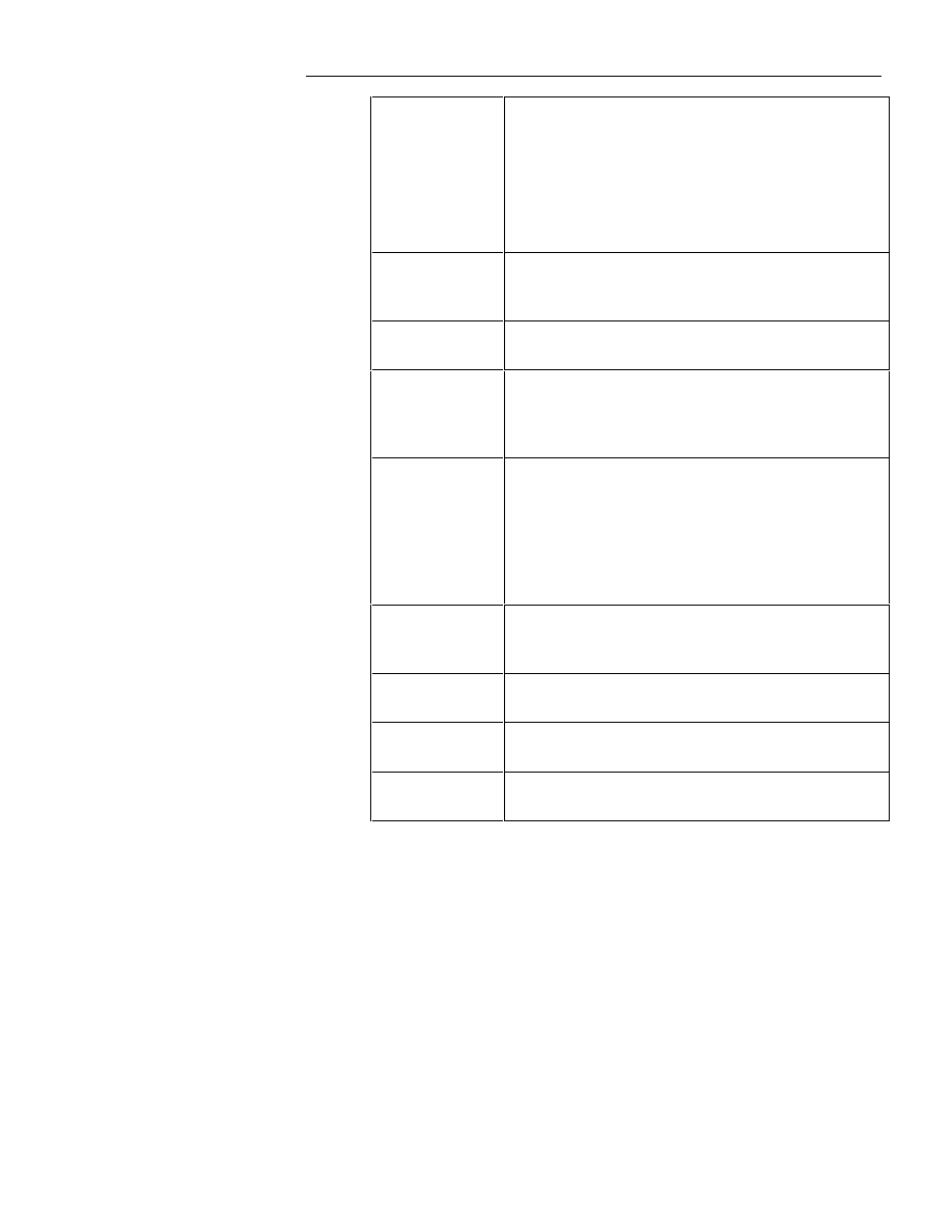
&KDSWHU6SHFFWUD,QWHUIDFH
201
Smart Grid
When this is enabled Specctra will calculate a grid
for the Via that will allow two tracks between two
vias. This grid will be used during the first 3
passes, after that it will resume the value set under
Via Grid.
Be aware that you could use vias as test points,
and hence they should be placed on a 25 mil grid.
Bus Diagonal
If you select this option, the first routing pass will
be for bus routing. The bus routing routes only
regular arrays, such as memory.
Protect All Wires
Will lock all the routed bus connections so that
they won’t be moved on subsequent routing passes.
Via Under SMD
Allows Specctra to place a via under an SMD pad.
Check with your manufacturer before making this
setting. Using this option will usually add
considerable manufacturing cost to your board.
Route Pass 1
Specifies the number of passes in the first route
batch. The default value is 25. The router stops
automatically if it encounters a complete route
pass and skips the rest of the routing passes,
jumping to the next command. For two layer
boards specify a higher number than 25: typically
50-200 passes.
Clean Pass 1
The number of cleanup passes after the first route
pass. Cleanup removes unnecessary vias, and
shortens tracks. The default setting is 4.
Route Pass 2
Set the Start Pass number for the second routing
pass, default value is 100.
Route Start 2
Specifies the number of passes in the second
routing batch. The default value is 16.
Clean Pass 2
The number of cleanup passes after the second
route pass. The default setting is 8.
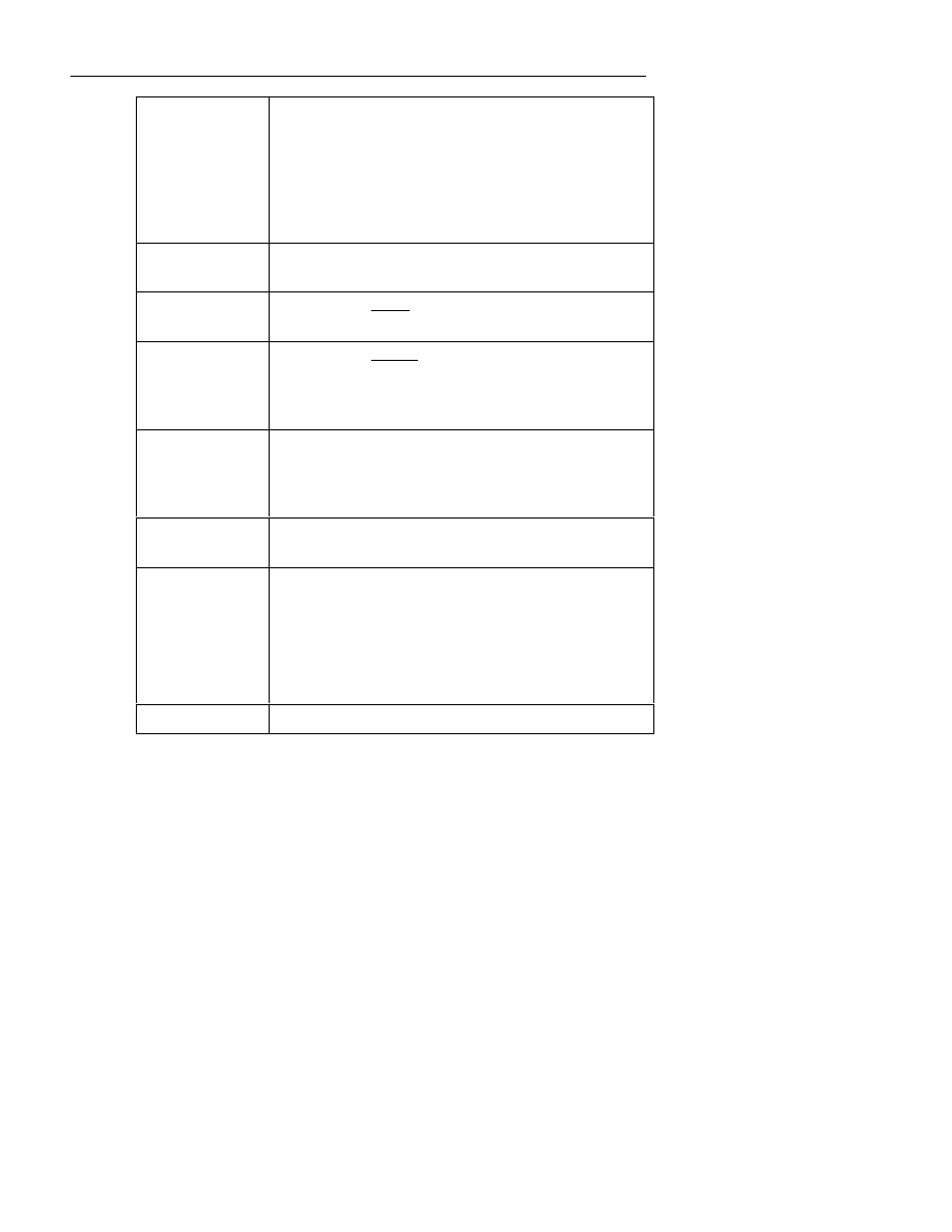
:LQ%RDUG/D\RXW5HIHUHQFH*XLGH
202
Use Fanout
On SMD boards with more than 2 routing layers,
enable this option to allow the Wires to "escape"
from SMD components by placing a via. See the
Specctra documentation for more information. It is
recommended that you not use Fanout on two layer
boards. Instead, increase the number of routing
passes to 50 or above.
Fanout Passes
Number of fan out passes to perform. Normal
setting for a complex SMD board will be around 5.
Fan In
Uses Fanout inside SMD components. The vias are
placed inside the boundry of SMD’s.
Fan Out
Uses Fanout outside SMD components. In the case
where both Fan In and Fan Out are enabled,
fanout will be performed both inside and outside
the components.
Power Only
Enabling this option will limit the Fanout to be
performed on Power nets only. (Please see Zones
regarding issues pertaining to the defining of
power nets).
Specctra Path
Define where
SPECCTRA.EXE
is. Use the file
browse to locate
SPECCTRA.EXE
.
Execute
If you choose to use the DO File, Execute will
convert a WinBoard board file to the Specctra
format and launch Specctra. When finished, you
will have a "session" output file.
If DO file is not selected, Execute will just output
a Specctra-format file (*.DSN).
Close
Leaves the WB2CCT program.
Layer Properties
Use Layer Properties to assign nets to a board layer that the Specctra should
not route. This is used for specifying nets such as ground planes that do not
need to be routed because there will be a copper pour area making the
connections.
&KDSWHU6SHFFWUD,QWHUIDFH
203
When you specify the WinBoard Placed File, each layer in the placed file is
listed in the area under Layer. Also, each net on the board is listed in the
pull-down menu next to Net.
Click Add Net to assign a net name to a specified layer. First select a layer,
then click Add Net to assign it.
Click Delete to remove an assigned net.
Example:
1.
Enter a board name in the WinBoard Placed File entry box.
2.
Select a layer for the ground plane under the list Layer.
3.
Select a net such as GND from the pull down box next to Net.
4.
Click the Add Net button. The GND net will now appear next to the
layer selected and will be listed under Net Assigned.
Click the Execute button to launch Specctra and route the board. When
Specctra is done, it will automatically return to the Interface (WB2CCT) and
the button To WinBoard will be enabled.
Click the To WinBoard button to launch the CCT2WB interface to complete
the process. See the instructions for CCT2WB.
CCT Specctra to WinBoard (CCT2WB)
If you manually launched Specctra (without using a Do File) click on the
CCT2WB icon shown at left in the Ivex Program Group. This will load the
CCT2WB Interface.
If you used a Do File to automatically launch Specctra, it will return to the
WB2CCT Interface when complete and the To WinBoard button will be
enabled. Click on the To WinBoard button to load the CCT2WB
Interface.
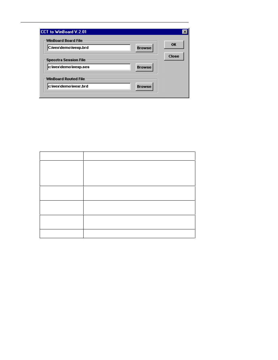
:LQ%RDUG/D\RXW5HIHUHQFH*XLGH
204
Figure 5.2 : The CCT2WB dialog box.
The CCT2WB dialog box has three inputs, the WinBoard Board File that
has the name of the original placed board, the Specctra Session File which
contains the autorouting results, and the WinBoard Routed File which is the
name for the new routed board file.
Option
Explanation
Specctra Session
File
The session file is generated when running the DO
file. If you run Specctra manually, you will have to
be sure to save the session file when you have
finished routing.
WinBoard
Board File
Identifies the original WinBoard file which holds
the module placement information.
WinBoard
Routed File
The name for the new board file that will contain
the routed board.
OK
Performs the merge function and saves the routed
board file.
Exit
Leaves the program.
If you used a Do File to automatically launch Specctra, these three boxes will
be filled with the correct file names. If you manually launched Specctra
without using a Do File, then you will need to enter the correct file names.

&KDSWHU6SHFFWUD,QWHUIDFH
205
Click the OK button to merge the Session file with the placed board file.
This will complete the process and save the new routed board in the file
specified as the WinBoard Routed File.
Return to WinBoard and load the new routed board file using the Tools |
Load Routed Board menu selection. It is important to use this menu
selection to properly merge the netlist parameters such as track isolation into
the completed board file. After loading the routed board file, save it using
the File | Save menu.
Tutorial
This short tutorial gives you a quick tour of the routing process with
Specctra. Very often you will be able to route your board with the DO file
options that are available in the WB2CCT program. Specctra’s advanced
(optional) features are beyond the scope of this tutorial. Refer to the Specctra
documentation for guidance in their use.
1.
Open WinBoard.
2.
Load
NEWDEMO.BRD
(a partially routed demonstration board file), and
look at it.
3.
Click on the Tools | Autoroute menu to launch the WinRoute program.
The WinRoute dialog box appears. Notice that the name of the currently
open board file is automatically entered in the space WinBoard Placed
File.
4.
Click the Browse button next to WinBoard Routed File and enter a new
board name such as
NEWX.BRD
.
5.
Check the box next to Use Do File. This will enable the automatic
execution of the Specctra router.
6.
Click on the Execute button to begin. The Interface automatically
launches the Specctra router.
7.
After Specctra has finished it's Routing and Cleaning passes, it will return
to the WinRoute dialog box and enable the To WinBoard button.
8.
Click the To WinBoard button. This will open the CCT2WB dialog box.
Verify that the file names in the three dialog boxes are correct.

:LQ%RDUG/D\RXW5HIHUHQFH*XLGH
206
9.
Click the OK button.
10.
Return to WinBoard and select Tools | Open Routed Board. This will
open the board file that Specctra just routed.
11.
Select File | Save and save the routed board file. You may use the
existing file name.
It is very easy to run the Specctra router. Most boards can be routed using
only the DO file, and the associated options.
Advanced Use
In case you need to control more routing parameters than possible with the
WinRoute interface, you will have to use a slightly different approach:
1.
Convert the board with the WinRoute program, but disable the DO file
option, as that will cause the interface only to generate a .DSN file.
2.
Load the .DSN file into Specctra following their documentation.
3.
When done routing, save a Session file.
4.
Now load the CCT2WB program, and merge the original Board file, with
the Session file into a new board file.
Power Planes
If you chose netnames such as VCC or GND to be associated with specific
layers, no routing will have been done on those layers. After Specctra has
finished signal routing, place copper zones on those layers to form the power
planes as desired, being careful to specify the netname correctly for each
copper zone created.
If you want split power planes you only need to place several zones with
different net names on the same layer. For example, to have a split power
plane with three areas, connected to AGND, DGND and CGND on layer 3,
place the three zones on layer 3 and assign the appropriate net names to each
of the power zones.
For more information, refer to the case study on the Ivex web site called
“How to create split power planes” in the Technical Support section.

&KDSWHU6SHFFWUD,QWHUIDFH
207
F
NOTE: The only way to tell Specctra that a net is a power net is to
associate that net with a specific layer, as described in “Using the Interface”
section above.
Limitations
Because WinBoard and Specctra handle objects differently, there are some
limitations about which you should know.
•
The main limitation is that Specctra does not handle arcs in a polygon
(copper zone) or in a board edge.
•
Copper zones should be placed AFTER all signal routing is completed,
as the last step!
•
Since Specctra does not handle arcs, all arcs in zones and board edge will
be substituted with line segments. But because only tracks are merged
onto the board file, the original zones or outlines containing arcs will still
be on the board. You only need to check that no traces are overlapping
the arc segments by running DRC.
•
The resolution is preset to 0.1 mil and cannot be changed. Only mil units
are supported.
The following objects will be represented as keep-out areas in Specctra:
mounting holes, targets and copper text.
•
Only through vias are supported (no blind or buried vias).
•
The part of the interface that merges the routed tracks into WinBoard
reads the tracks from the Session file, and does not transfer any module
information. Modules come only from the original board file. So you
cannot move modules in Specctra.


Appendix A: Importing Netlists
Appendix A describes importing netlists from other vendor’s schematics.
Additions to Appendix A may come later as Application notes.
Importing an Orcad Schematic Netlist
You can create netlists from within Orcad SDT for WinBoard. We have
supplied you with netlist utilities that create WinBoard netlists from within
Orcad SDT. To create WinBoard netlists with your Orcad SDT product, you
must be sure that the netlist utilities are installed in the correct directories.
In addition, WinBoard has the following advanced options that you can use
with Orcad SDT:
•
You can assign net properties to nets directly from within the schematics.
This enables the system to remember specific tracks that should have
more distance between them and other tracks. This is commonly done to
prevent noise with high voltage tracks.
•
When you assign module names in WinBoard, the names are
automatically fed back into the Orcad schematics.
You need to have a working knowledge of the Orcad tools to use the
interface between Orcad and WinBoard. If you have any questions regarding
the Orcad products, please refer to your Orcad documentation.
Installing the Orcad Interface
Orcad's netlist language has changed from version to version, and they have
two different formats: 16 bit and 32 bit. Therefore, we have provided four
separate utilities for different netlist versions. The utilities are installed in the
netforms
subdirectory (
c:\ivex\winboard\netforms
) and are
listed by directory name below:

:LQ%RDUG/D\RXW5HIHUHQFH*XLGH
210
netforms\SDTIV.40X\FwinBrd.cf
Orcad SDT IV version 4.0X
netforms \SDTIV.41X\FwinBrd.cf
Orcad SDT IV version 4.10 and
later
netforms \SDT386.10X\FwinBrd.exe
Orcad SDT 386 version 1.0X
netforms \SDT386.11X\FwinBrd.exe
Orcad SDT 386+ version 1.1X
or later
netforms \capture\FwinBrd.dll
Orcad Capture
In the file names and version numbers above, the x denotes any number
between zero and nine. 4.0X includes any number from 4.00 through 4.09.
F
NOTE: There is no netlist format available for SDT version 3.XX because no
netlist formatter was supplied by Orcad with those versions. To transfer
schematic information into WinBoard, you will have to choose another netlist
format. We recommend either EDIF or Protel format. Both of these formats
will work. However, you will not be able to write the footprint module names
back to your schematic or assign net properties.
Place your WinBoard product disk number one in your "A" drive and change
to the netlist directory on the "A" drive.
To identify where you need to install the netlist formatter, you can enter the
following DOS command:
C:\> SET
A long list of settings displays. You need to find a section that looks similar
to the following:
SET ORCADEXE=C:\ORCADEXE\
SET ORCADESP=C:\ORCADESP\
SET ORCADPROJ=C:\ORCAD\
SET ORCADUSER=C:\ORCADESP\
Find the line that begins with
SET ORCADESP=
. Make a note of the path
that follows the equal sign and copy the correct netlist formatter to a directory
with that path name, followed by
\SDT\NETFORMS
.

$SSHQGL[$,PSRUWLQJD6FKHPDWLF1HWOLVW
211
For example, if you had Orcad SDT 386 version 1.10, you would copy the
files with the following command:
COPY a:\netlist\orcad386.11x\*.* c:\orcadesp\sdt\netforms.
After the file
fwinbrd.exe
(
fwinbrd.cf
for SDT IV) is copied to the
c:\orcadesp\sdt\netforms
directory, you need to configure Orcad
to generate a WinBoard netlist format instead of the netlist format it is
currently set to generate. To re configure Orcad to generate netlists in
WinBoard netlist format, follow these steps:
1.
Start Orcad.
2.
Change to the Template Design.
3.
Select the Netlist button.
4.
Select Local Configuration.
5.
Select IFORM.
6.
In the Netlist format list box, click on FWINBRD.EXE.
7.
Click OK.
Now you are ready to create a WinBoard netlist. Every time you create a new
project, WinBoard format will automatically be configured for netlists. If you
have an existing design for which you want a WinBoard netlist, follow these
steps:
1.
Start Orcad.
2.
Change to the design for which you want an WinBoard netlist.
3.
Follow steps three through seven above.
Net Properties
You can control the net width and other related properties with the "Pipe"
function in Orcad. The following text is an example of the net property text
you need to place on your root level schematic:
|WINBOARD
|DEFAULT 15mil 12mil 35mil 17mil
|AD0 12mil
Each line must start with the pipe symbol:
|
. The first line must be:
|WINBOARD

:LQ%RDUG/D\RXW5HIHUHQFH*XLGH
212
It is important that
WINBOARD
be all in upper-case letters.
One line must follow another without any blank lines.
If you fail to specify the default net setting on the schematic, WinBoard’s
default setting will be used. Any properties you fail to specify on the
schematic default to WinBoard’s default settings.
The first command must be the net identification. However, you may define
as many or as few net properties aslong as you follow the coorect order of
apperance.
The net properties you can define are listed below followed by a list of
variables and explanations of each variable. Properties enclosed in square
braces are optional. For example, you need not specify units if you want to
use mils. However, if you prefer millimeters (mm) or microns (um), you must
specify the units you need.
net_name
twidth[unit]
isolation[unit]
via[unit],drill[unit]
allowed_layer, allowed_layer
nettype
twidth
The track width.
unit
The units in which the identifier is specified: mil (1/1000 inch),
mm (millimeter), or um (microns). Mil is the default when
nothing
is specified.
isolation
The Isolation from track to other copper.
via
The via size.
drill
The drill size for the via.
allowed_layer
A layer allowed for routing.
*
Any layer.
C
Component layer.
S
Solder layer.
+1
The first layer above the solder layer.

$SSHQGL[$,PSRUWLQJD6FKHPDWLF1HWOLVW
213
-1
The first layer below the component layer.
nettype
T = Tree net. C = Chained net.
An example of a pipe command is shown below:
|WINBOARD
|DEFAULT 12mil 8mil 35,17 * T
|110V 35mil 45mil 55,12 -1,1
Assigning Footprint Modules
For each part, Orcad has a Reference field, a Part Value field, and eight
general Part fields. By using one of these general part fields, you can assign
WinBoard’s footprint module names to each component. To use Part Field 1
as the module part field, follow these steps:
1.
Start Orcad and select Schematic Design Tools.
2.
Select Configure Schematic Tools. The Configure Schematic Design
Tools screen displays.
3.
Move the pointer down to the Color Table section of the Configure
Schematic Design Tools screen.
4.
Hold down the left mouse button and drag the pointer across the text in
the 1ST PART FIELD text entry box. The text becomes highlighted.
5.
Replace the text with the name used by WinBoard for the module.
6.
Move the pointer down to the Key Fields section of the Configure
Schematic Design Tools screen.
7.
Just under Create Netlist, click in the Module Value Combine text
entry box and enter
1
.
8.
Select Home and click OK.
You can choose to assign WinBoard footprint module names to each
component on the schematic now, or you can assign them later when you
load the netlist into WinBoard. You can also choose to assign footprint
module names to as many or as few components as you like. It is NOT
necessary to assign footprint module names to every component if you don’t
want to.

:LQ%RDUG/D\RXW5HIHUHQFH*XLGH
214
The modules you assign in WinBoard can later be automatically inserted into
your schematics. For information about automatically inserting the modules
into your schematic, refer to Loading Netlists in Chapter 2: Menu and
Toolbar Reference.
Netlist Import: Tango and Protel
The Tango and Protel netlist formats have been changed in version 2.0 to
take into account different “flavor” of the netlist format. The basic change is
that it will automatically recognize where the Part Value from the device is
placed.
The basic Component in Tango and Protel netlist format is described as
below.
[
U9
20DIP300
74LS346
]
[
R1
RC06
RES
100K
]
In the example above, there are two modules, U9, and R1. The 1.11 netlist
reader would always use the third item, as the Module Part Value, but some
products generating Tango netlist use that field for “Type” description, such
as RES. The 2.0 version of the netlist reader will automatically detect that a
fourth field is used, and use it as the Part Value.
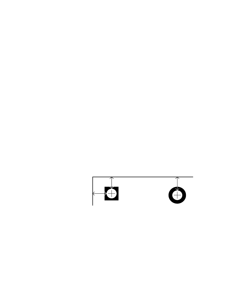
Appendix B: DRC Definitions
This Appendix defines the terms used by the Design Rule Checking tools.
Drill to other objects
This section of the appendix defines the distance between drill holes and
other objects.
Drill-Min./Max.
Drill-Min. and Drill-Max. define the minimum and maximum drill size for
drill holes, vias, and through hole pads. This parameter is useful because
many board manufacturer’s NC machines can only handle particular
minimum and maximum hole sizes. If the hole is too big it needs to be cut out
by an NC machine. The Drill-Min. and Drill-Max. size is the diameter of the
drill.
Drill-Edge
Drill-Edge spacing is the shortest distance from the outside of the drill hole
to the center of the board edge line.
Drill hole to edge spacing
Figure B-1. Drill hole to edge spacing.
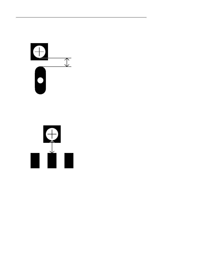
:LQ%RDUG/D\RXW5HIHUHQFH*XLGH
216
Drill-Pad
Drill-Pad is the minimum distance allowed from a drill hole copper outline,
to the copper of a pad.
Drill to pad spacing
Figure B-2. Drill to pad spacing.
Drill-SMD
Drill-SMD is the minimum distance between the SMD pad and the drill hole.
Drill to SMD pad minimum distance
Figure B-3. Drill to SMD pad minimum distance.
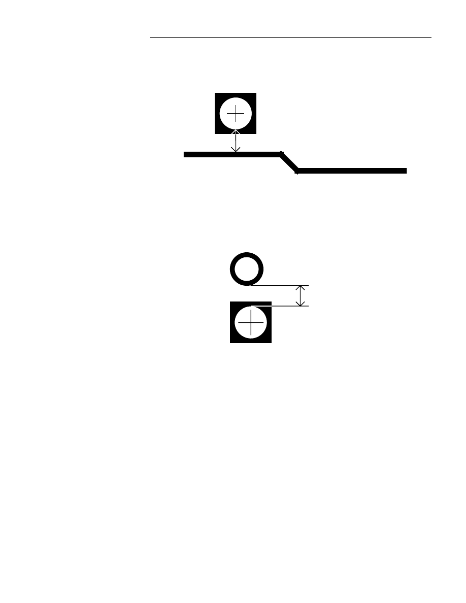
$SSHQGL[%'5&0DWUL['HILQLWLRQV
217
Drill-Track
Drill-Track is the minimum distance allowed between the outer copper of
the drill hole and the nearest track edge.
Drill to track spacing
Figure B-4. Drill to track spacing.
Drill-Via
Drill-Via is the minimum distance between the outer copper of the drill hole
and the via copper.
Via
Drill Hole
Drill hole to via spacing
Figure B-5. Drill hole to via spacing.
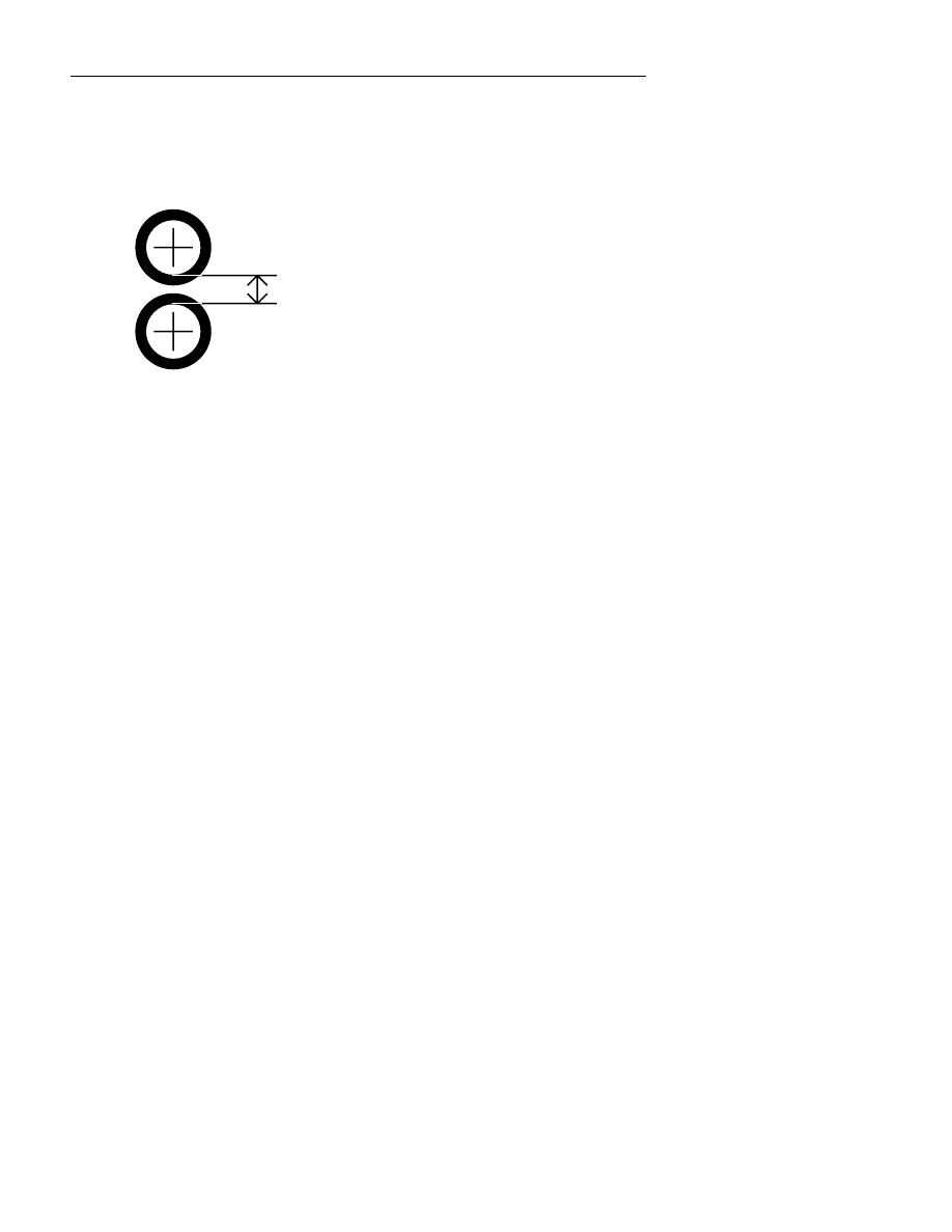
:LQ%RDUG/D\RXW5HIHUHQFH*XLGH
218
Drill-Drill
Drill-Drill is the minimum distance between the outside edges of any two
drill holes. These drill holes are vias, pads, or actual drill holes. With Drill-
Drill, any distance from a drill hole to the edge is also checked for.
Drill to drill spacing
B-6. Drill to drill spacing.
Via to other objects
This section of the appendix defines the distance between vias and other
objects.
Via Min./Via Max.
Via Min. and Via Max. are the minimum and maximum diameter allowed
for vias on the board.
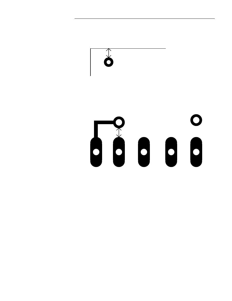
$SSHQGL[%'5&0DWUL['HILQLWLRQV
219
Via-Edge
Via-Edge are the minimum distance allowed from the edge of the via to any
board edge.
Board edge
Via to board edge minimum distance
Figure B-7. Via to board edge minimum distance.
Via-Pad
Via-Pad is the minimum distance between the outside edge on a via to the
outside edge of a Pad.
Via to pad isolation
Figure B-8. Via to pad isolation.
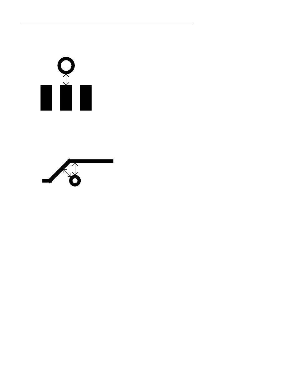
:LQ%RDUG/D\RXW5HIHUHQFH*XLGH
220
Via-SMD
Via-SMD is the via to SMD isolation distance is defined as the minimum
distance from the outside edge of the via, to nearest point on the SMD pad.
Via to SMD isolation
Figure B-9. Via to SMD isolation.
Via-Track
Via-Track is the minimum distance from the outer copper edge of the via to
the outer edge of the track.
Via to track minimum distance
Figure B-10. Via to track minimum distance.
Via-Via
Via-Via is the minimum distance between the outer edge of one via to the
outer copper edge on any other via.
Tracks to other objects
This section of the appendix defines the distance between tracks and other
objects.
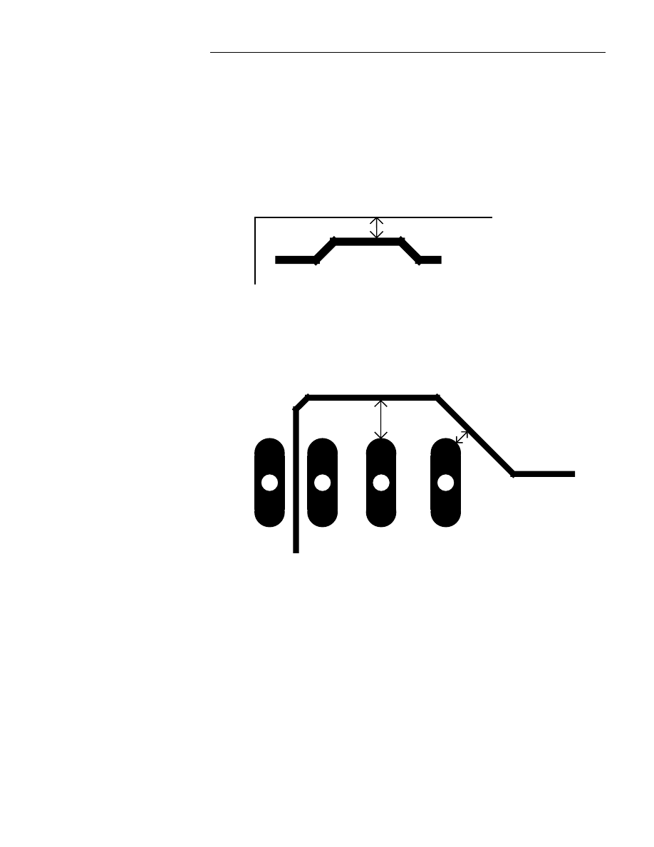
$SSHQGL[%'5&0DWUL['HILQLWLRQV
221
Track-Min./Track-Max.
Track-Min. and Track-Max. are the minimum and maximum width of a
track anywhere on the board.
Track-Edge
Track-Edge is the track to edge spacing calculated from the center of the
board edge to the outside of the track.
Board Edge
Edge to track spacing
Figure B-11. Edge to track spacing.
Track-Pad
Track-Pad is the minimum allowed space from any track to any pad on the
board.
Figure B-12. Track to pad spacing.
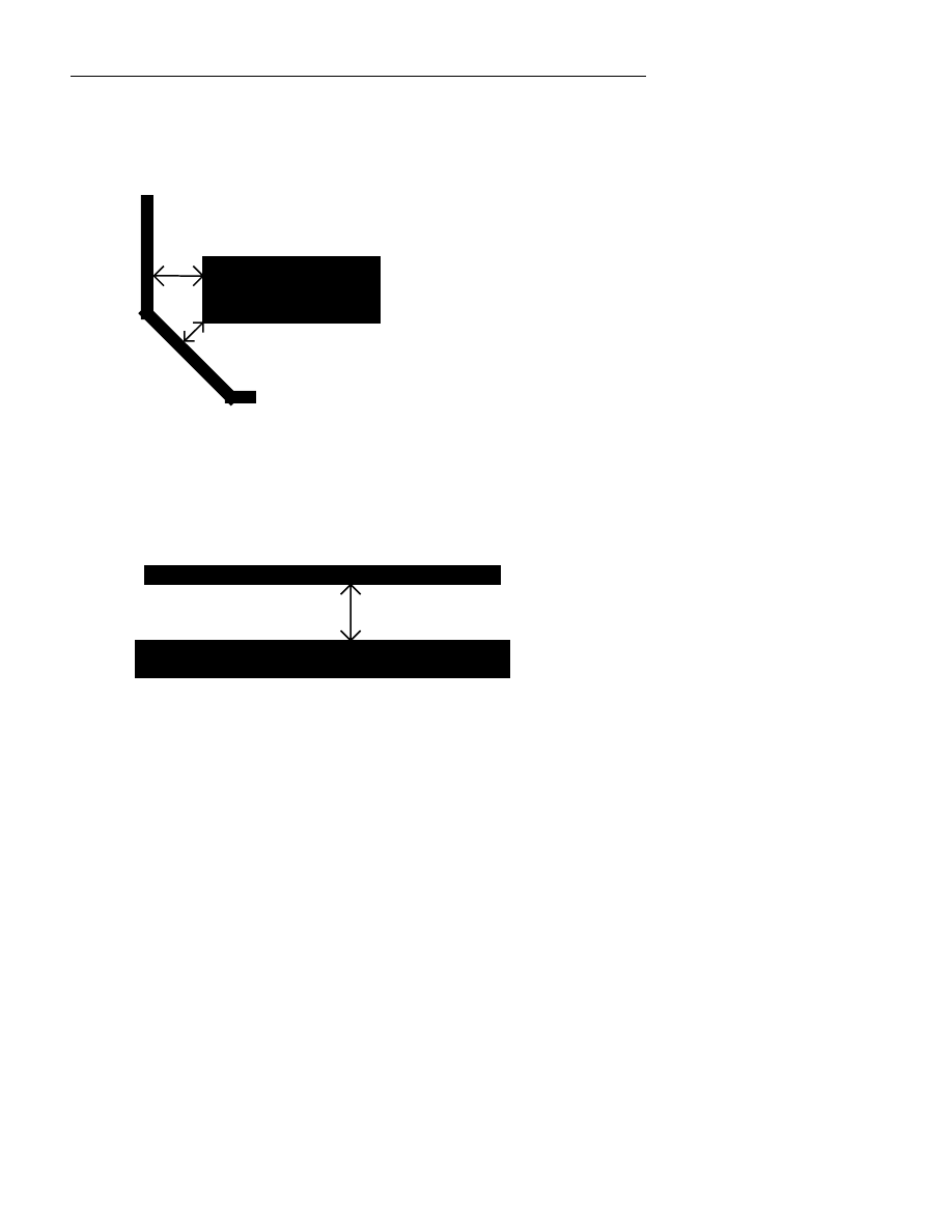
:LQ%RDUG/D\RXW5HIHUHQFH*XLGH
222
Track-SMD
Track-SMD is the minimum distance from any track to any SMD pad on the
board.
SMD pad to any track
Figure B-13. SMD pad to any track.
Track-Track
Track-Track is the minimum track to track spacing allowed between two
tracks.
Track to track spacing
Figure B-14. Track to track spacing.
SMD to other objects
This section of the appendix defines the distance between SMD pads and
other objects.
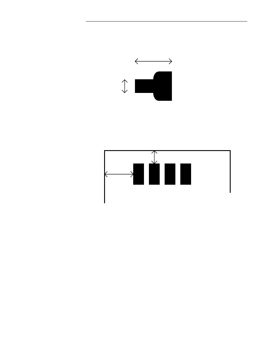
$SSHQGL[%'5&0DWUL['HILQLWLRQV
223
SMD-Min./SMD-Max.
SMD-Min. and SMD-Max. is the minimum distance in any direction, and
the maximum distance in any direction. In the case of pad stacks, it will be
the minimum and maximum distance in any angle or direction.
Min.
Max
Complex SMD
Figure B-15. SMD minimum/maximum.
SMD-Edge
SMD-Edge is the minimum distance from any SMD pad to any edge on the
board. The distance is defined as the distance from the center of the edge to
the outside edge of the SMD pad.
SMD to edge isolation
Figure B-16. SMD to edge isolation.
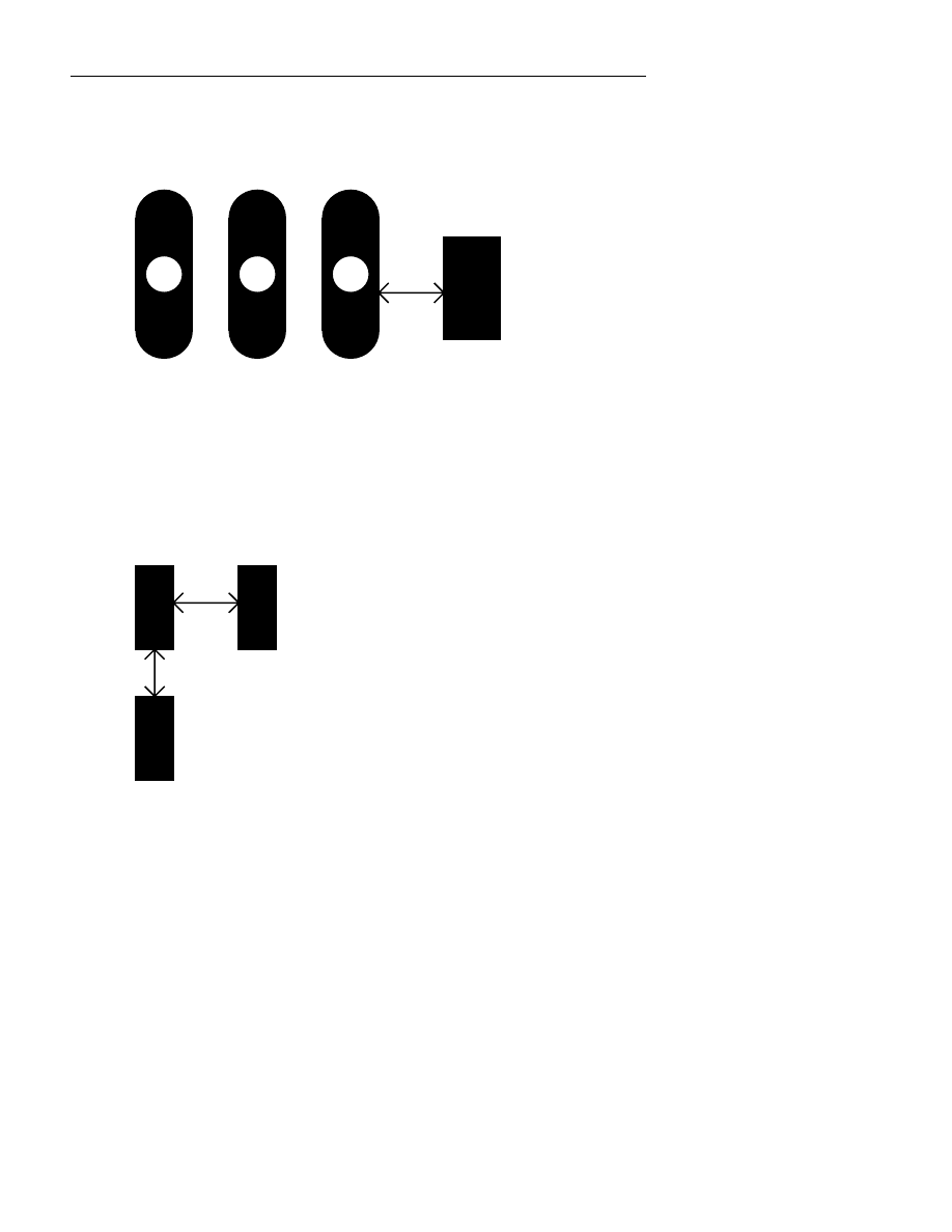
:LQ%RDUG/D\RXW5HIHUHQFH*XLGH
224
SMD-Pad
SMD-Pad is the minimum distance from any SMD pad to any through hole
pad.
SMD to pad isolation
Figure B-17. SMD to pad isolation.
SMD-SMD
SMD-SMD is the minimum distance between any SMD pad to any SMD
pad.
SMD to SMD minimum isolation
B-18. SMD to SMD minimum isolation.
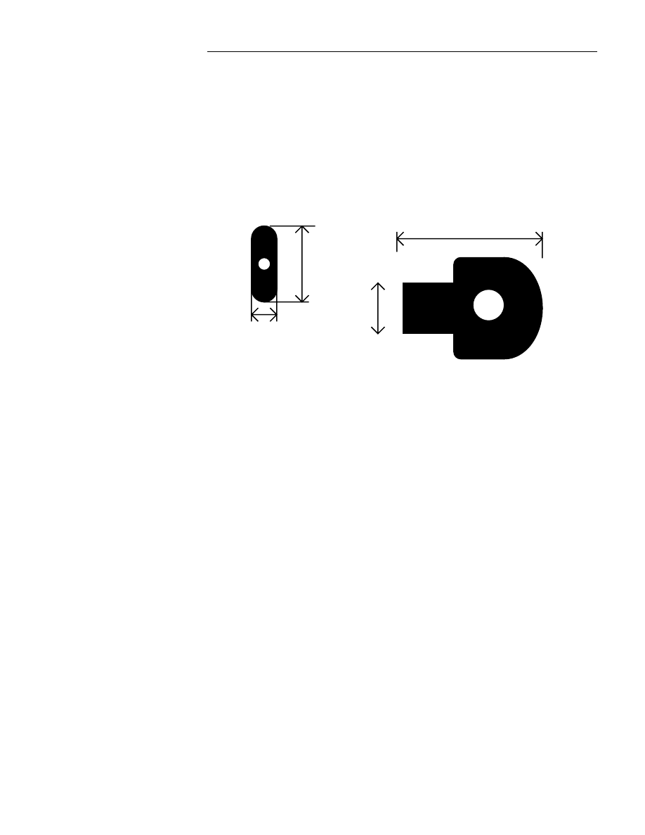
$SSHQGL[%'5&0DWUL['HILQLWLRQV
225
PAD to other objects
This section of the appendix defines the distance between through pads and
other objects.
Pad-Min./Pad-Max.
Pad-Min. and Pad-Max. are the absolute minimum and maximum size in
any direction.
Maximum
Complex PADSTACK
Minimum pad size
Figure B-19. Pad minimum/maximum.
Pad-Edge
Pad-Edge is the minimum distance from any through hole pad to any board
edge. The distance is from the center of the edge line, to the outer edge of the
pad.
Pad-Pad
Pad-Pad is the minimum distance from any through hole pad to any other
through hole pad, measured as the outside edge of the copper to the outside
edge of the copper.

:LQ%RDUG/D\RXW5HIHUHQFH*XLGH
226
Annular-Min./Annular-Max.
Annular-Min. and Annular-Max. checks the annular ring of through hole
pads, and vias. The number is calculated as (Pad radius - Drill radius).
Minimum/maximum annular ring
Figure B-20. Minimum/maximum Annular ring.
Zone
This section of the appendix defines the minimum zone width.
Zone-Min.
Zone-Min. is the zone minimum width at any point. The idea of this setting
is to find any place where the zone may be too narrow and there may be a
risk that the zone will be etched away, leaving floating copper areas.
Appendix C: Keyboard
Commands & Extensions
There are some commands you may enter simply by pressing one key on the
keyboard. These commands are listed in the tables below. You may also
easily find these commands on-line by selecting
Help | Key Commands
in the program.
Key Commands:
Track, Outline, and Edge Editing or Routing and other keyboard shortcuts.
Key
Command Description
r
Route a track with Track, Outline & Edge routing mode.
b
Begin or continue placing vertices when placing a track, outline,
or edge.
g
Use to toggle On or Off grid.
i
Use to open Density Map dialog box.
l
Use the L key on the keyboard to reset the Origin bookmark to
the screen origin.
m
Route more connections while in routing mode by pressing
m
.
This tells WinBoard to show the ratsnest for the next connection
on the netlist.
n
End a track, outline, or edge with the
n
key. WinBoard remains
in the placement mode so you can continue placing tracks,
outlines, or edges.
Back
space
Backtrack or undo a segment while placing a track, outline, or
edge.
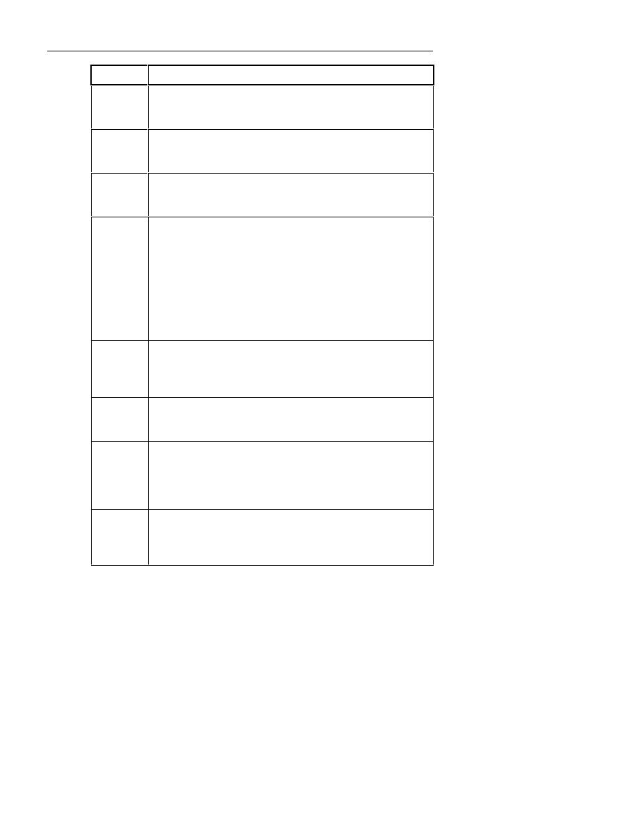
:LQ%RDUG/D\RXW5HIHUHQFH*XLGH
228
Key
Command Description
c
or
-
Change to the next lower numbered layer and place a via while
routing a track by pressing
c
. Repeatedly pressing
c
will
continue to change layers until the solder side is reached.
v
or
+
Change to the next higher numbered layer and place a via while
routing a track by pressing
v
. Repeatedly pressing
v
will
continue to change layers until the component side is reached.
s
Change the style while placing a track, outline, or edge.
s
mirrors the current track, outline, or edge segments around the
location of the pointer.
w
Display the Track Parameter dialog box while routing a
track by pressing
w.
The Track Parameter dialog box
makes it possible for you to change:
1.
The track width of the track segments after the current vertex.
2.
The via diameter of all of the vias associated with the track
after the current vertex of the track.
3.
The drill size of all of the vias associated with the track after
the current vertex of the track.
x
Toggle through the routing style with
x
: 45
°
, 90
°
, any angle,
and arc. Each time the
x
key is pressed, the Track, Outline &
Edge button changes to reflect the current routing angle or
arc.
Shift
Drag four track vertices at once by holding down the
Shift
key
while clicking on the Track, Outline & Edge button. For more
information, see Chapter 1: Editing Features.
Shift +
Ctrl
Drag a whole track at once while leaving the beginning and
ending points of the track untouched by holding down the
Shift
and
Ctrl
keys while clicking on the Track, Outline &
Edge button. For more information, see Chapter 1: Editing
Features.
Space
Bar
To edit a Module Outline. Hold down the Space Bar to edit the
module outline on a board. (This is not necessary in the Module
Editor.) Select the outline by holding down the Ctrl key and
click with the left mouse button
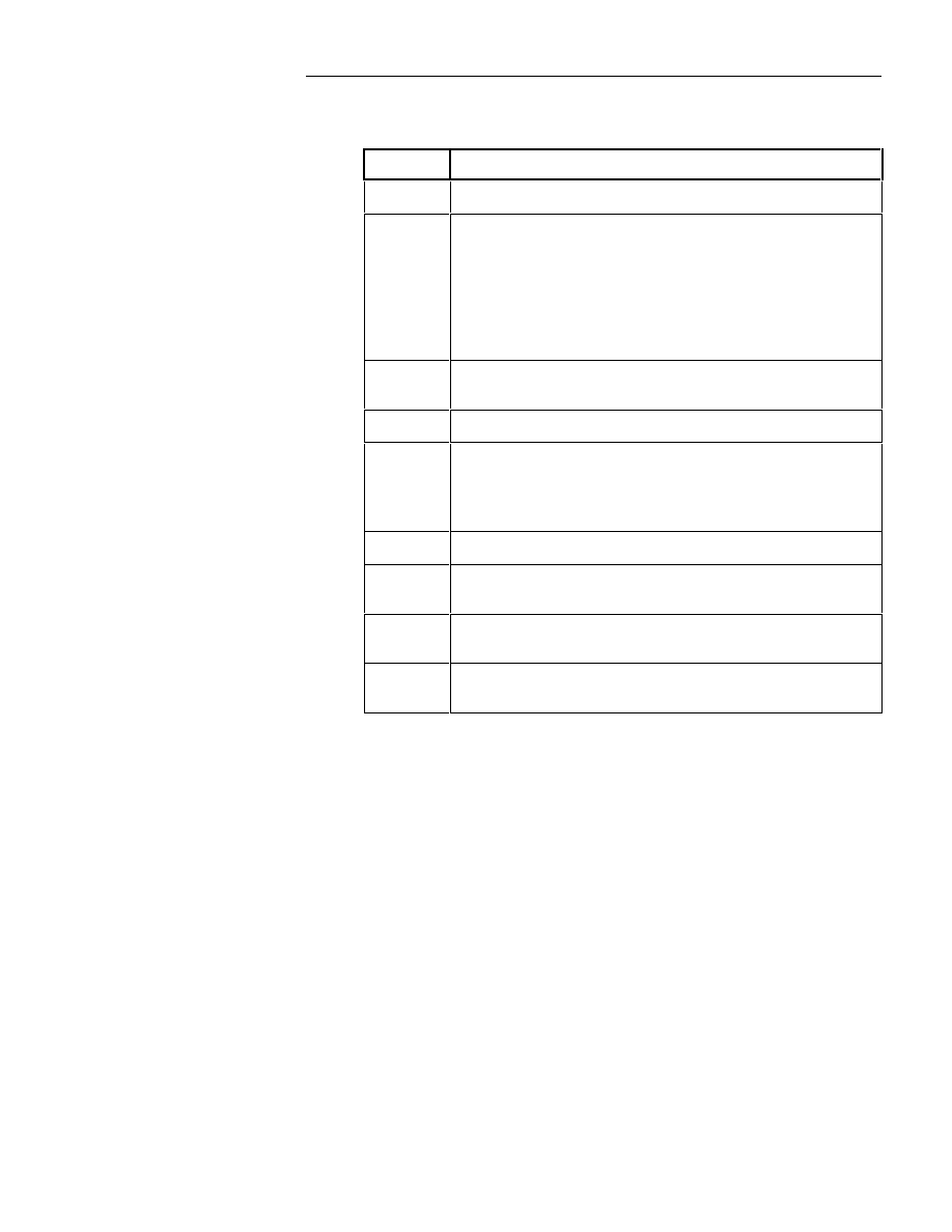
$SSHQGL[&.H\ERDUG&RPPDQGV
229
Function Key Commands
Key
Command Description
F1
Display online Help.
F2
Inquiry : Display pad and track information by pointing at
a pad or route and pressing
F2
. For pads,
F2
displays the
net name, module name, and pin number. For routes,
F2
displays the net name, connection by module name and pin
number, and track length. The information is displayed in
the Windows status bar located at the lower left corner of
the screen.
F3
Global Edit tool. For information about Global Edit, refer to
Global Edit in Chapter 2: Menu and Toolbar Reference.
F4
Rebuild netlist.
F5
Select & Highlight net. Place the cursor over the track to
highlight and press the F5 key. This also shows the Total Net
Length of the net in the Windows status area at the lower left
corner of the screen.
F6
Toggles ratsnest visibility on/off.
F7
Compile Netlist on/off. Use for larger board (over 1000 pins)
to speed up compilation when placing or moving modules.
F8
Find, Get & Place Module. Use to place using X, Y
coordinates, etc.
F9
Display Total Ratsnest Length in the Windows status area at
the bottom left screen corner.
Numeric Key Pad Commands
The numeric key pad can be used to issue commands to WinBoard. The Num
Lock must be on for the numeric key pad to function correctly. The numeric
key pad is shown in the figure below with the command each key is used for.
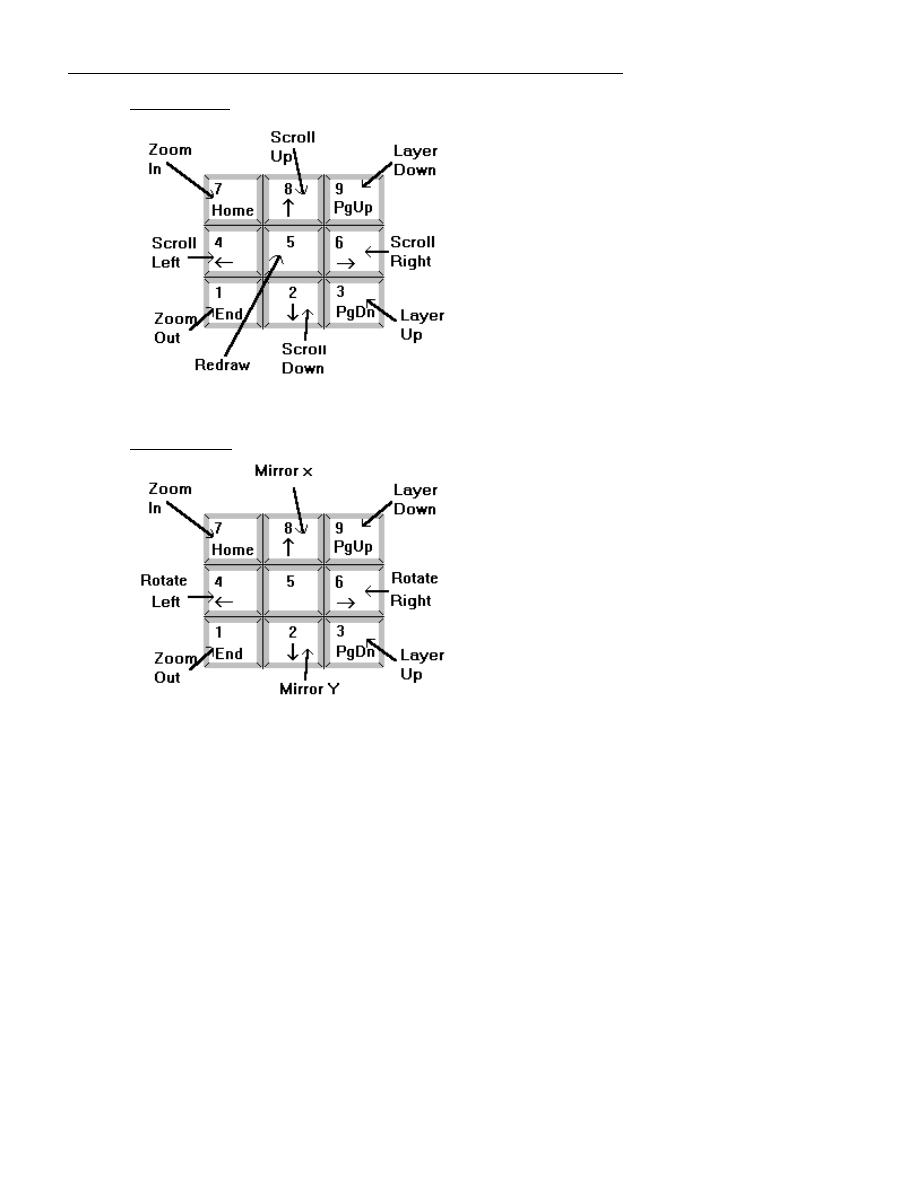
:LQ%RDUG/D\RXW5HIHUHQFH*XLGH
230
Num Lock On :
Num Lock Off :
The 1, 3, 7 and 9 keys have the same function with Num Lock on or off.
With Num Lock Off, the arrow keys (2,4,6,8) have the same function as the
arrow key next to the ten key pad.
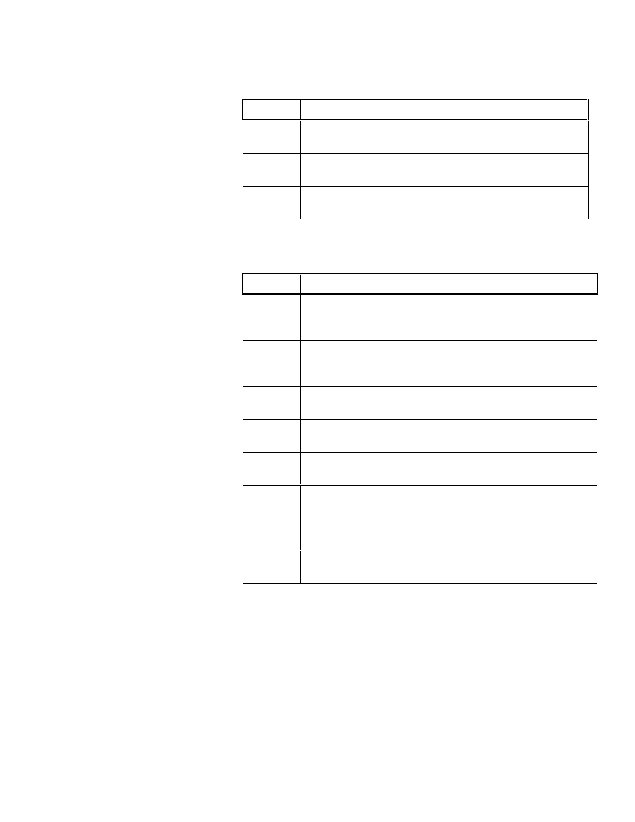
$SSHQGL[&.H\ERDUG&RPPDQGV
231
Screen Panning and Zooming Key Commands
Key
Command Description
Z
Refresh the screen with the current pointer location as the
center of the screen.
Home
Zoom in with the current pointer location as the center of
the screen.
End
Zoom out with the current pointer location as the center of
the screen.
Object Manipulation Key Commands
Key
Command Description
Æ
Flip a selected object or group of selected objects up around
the objects’ reference point. Flip and mirror object to the
other side of the board.
Ç
Flip a selected object or group of selected objects down
around the objects’ reference point. Flip and mirror object to
the other side of the board.
Å
Rotate a selected block of objects clockwise around the
center of the block of objects.
Ä
Rotate a selected block of objects counterclockwise around
the objects’ reference point.
Ctrl
Æ
Flip a selected block of objects up around the center of the
selected block.
Ctrl
Ç
Flip a selected block of objects down around the center of
the selected block.
Ctrl
Å
Rotate a selected block of objects clockwise around the
center of the selected block.
Ctrl
Ä
Rotate a selected block of objects counterclockwise around
the center of the selected block.
:LQ%RDUG/D\RXW5HIHUHQFH*XLGH
232
List of File Extensions
Function:
File Extension:
Netlist
.net
Gerber photo plot
.ger or .gbr
Aperture, D code
.pen
NC Drill Excellon
.drl
Through holes report
.th
Blind Via report
.l?
Buried Via report
.u?
Punch hole report
.p?
Pick & Place report
.pk? (pk1, pk2, pk3…)
Pick & Place report
summary
.pik
Bill of Materials (BOM)
.bom
In Circuit Test
.ict
Netlist Compare, Changes
.ncp
Netlist Was-Is
.ban
Pin List report
.pin
Place File report
.plc
MCL library source
.mod
Library file
.lib
DRC Spec
.spc
Template File
.tpl
Appendix D: Question/Answer
This chapter provides a reference for frequently asked questions. The format consists of a
problem or question and an answer or description on how to do it. For a more complete list
of hundreds of questions and answers, refer to the Ivex Knowledge Base located on our
web site (www.ivex.com).
Problem or Question:
How do I ...?
Answer:
Editing:
Change the track width of a
selected net?
Place the cursor on the track. Press the F2 key to identify
the net name on the status bar. With the cursor on the track
press the F5 key to highlight the net. Continue pressing the
F5 key on other nets if you want to change more than one
net. When all the nets are selected, press the F3 key to
bring up the Global Edit dialog box. Press the Track button
and enter the new track width. Press Ok to exit the dialog
box and make the changes.
Also, see explaination in Chapter 2 : Edit Netlist, Edit net
characteristics.
The program asks for the
registration when you start
the program.
The registration number is written back to the EXE file
and the program.
If you are on a network, check to see if you have
writing rights for the directory. Check with your
network administer.
Copy PCB.EXE to you local hard drive and run the
program. Type in the Registration number, quit the
PCB.EXE. Now copy the PCB.EXE back to the network.
:LQ%RDUG/D\RXW5HIHUHQFH*XLGH
234
Occasionally errors or
display problems.
If you experience occasional application errors, or a
situation where the system hangs, this may not be a function
of the program, but simply a bug in your current graphics
driver.
Go to your Windows Setup and select the standard
Windows driver for SVGA 800x600 and install. If problem
persists, contact your graphics driver provider, and ask for a
new driver. Often you will be able to download these from
the manufactorer BBS systems, their number is generally
stated in the manuals for the graphic cards. If a new driver
does not solve the problem, please contact Ivex.
Error message in netlist load:
Pin reference XXX not
found in Module YYY, part
reference ZZZ
This error occurs when pins described in the netlist do not
exist on the module footprint. It’s often seen in parts like
transistors that have pin names like “BASE” and
“EMITTER” on the schematic, instead of the expected “1”,
“2”, “3”, etc. You will need to update your schematic
library to use pin numbers instead of names on all parts.
How do I edit Module Part
value or reference text
Module text is a part of the modules, but may be selected
individually. Most objects in WinBoard you simply select
by clicking on them, but text and tracks on dense boards
often are overlapping so it would be difficult to choose one
to select. Therefore, to isolate text from other objects,
simply hold down the Ctrl key, and click to select or
double click the text to edit.
Can not see all of the X, Y
coordinates on the screen.
You are probably using VGA 640 x 480. Change to SVGA
800 x 600 and it is all visable. Windows includes 800 x 600
drivers and these greatly enhance the performance and
usablilty of your applications. Change under Windows
Setup in the Program Manager. Refer to your Windows
users manual for more details.
You may also use the floating x,y coordinate box. Select
Help | X Y Window.
$SSHQGL['4XHVWLRQ$QVZHU
235
The printer does not seem to
print properly.
Printing is primarily a function of Windows and the print
driver. If you experience problem, the first step should be
to contact your printer manufacturer for an updated driver.
The next step should be to contact Microsoft to determine if
there are problems with Windows using certain printers or
drivers.
Where is my Gerber aperture
file?
If you are using the format 274-D, you must generate a
separate aperture file. Refer to the section on Gerber in
Chapter 2. It is recommended that the format 274-X is used
as it is much newer and includes the aperture file.
It does not place a via when I
press the C or V key while
routing.
You must select the routing layers by holding down the Shift
key and clicking on the layer button. Selected layers have
RED numbers.
I can not select text or smd
pads by clicking on them.
You must be on the correct layer. First select the layer by
clicking on the layer button, then select the track or pad.

Glossary
Active Layer
The board layer that is currently being routed or edited.
Adhesive
Adhesive dots are used for attaching SMDs to the PC board in manufacturing.
Analog Circuit
A circuit made up mostly of discrete components such as resistors, capacitors,
and transistors, which produces data represented by a physical variable such as
voltage, resistance, or rotation.
Anchor point
The anchor point is the point around which a module rotates or turns and the
point from which all other measurements pertaining to the module are made. The
anchor point is usually located at pin one.
Aperture
A hole, such as that in a camera, that is used for Gerber photo plotting. Apertures
can be various sizes and shapes.
Artwork
A to-scale master pattern representing tracks and pads used to produce a printed
circuit board.
ASCII
An acronym for "American Standard Code for Information Interchange." A
seven-bit code representing alphanumeric and other instructions from a computer
keyboard, such as Enter, Backspace, and Delete.
ASIC
An acronym for "Application Specific Integrated Circuit."

*ORVVDU\
237
Autopan
A mode that automatically moves the viewing window when the pointer comes
up against the edge of the screen.
Blind Via
A pathway between two or more layers of a multi-layered PC board that only
reaches one outside layer of the board and has a copper pad on that outside layer
(usually the component side of the board). Vias are used to connect signals (or
tracks) between layers of a PC board.
Block
A particular section of a WinBoard file that is selected and manipulated as one
entity.
BookMark
Book marks are used to mark specific locations on WinBoard board files
enabling you to find them easily. You place a bookmark at a particular location
on the board file. Then when you are editing at a different location and want to
move back to the location of the bookmark, you use the BookMark button on the
toolbar to pan the screen back to the location of the bookmark.
Buried via
A pathway between two or more layers of a multi-layered PC board that does not
reach either outside surface of the board. The hole itself is coated with copper,
and is used to connect signals (or tracks) between layers of a PC board.
Bus
A thick track or conductive metal strip on a PC board used to connect a series of
smaller tracks together and distribute voltage, grounds, and so on.
CAD
An acronym for "Computer Aided Design."
CAE
An acronym for "Computer Aided Engineering."
CAM
An acronym for "Computer Aided Manufacturing."

:LQ%RDUG/D\RXW5HIHUHQFH*XLGH
238
Chamfer
A broken or cut corner on a printed circuit board edge used to eliminate an
otherwise sharp edge.
Clearance
The area around a pad, route, or via which must not intrude upon conductors of
another signal set.
CMOS
An acronym for "Complementary metal-oxide-semiconductor" integrated circuit.
Component Side
The top layer of the PC board on which most of the components are mounted.
WinBoard always uses the highest numbered layer for the component side.
Conductor
One single conductive path.
Contiguous segment
One continuous portion of a track with no bends or vias.
Copper Zone
A single area of a PC board covered with a layer of copper when manufactured.
Also known as a "metal zone."
Design on the Fly
The process of designing a PC board without a pre-existing schematic, or
changing the board design without the help of a schematic. The WinBoard Edit
Netlist/Netlist on the Fly tool can be used for designing on the fly.
Design Rules
Parameters that are used by the Design Rules tool to make sure that the isolations
between the pads and tracks on your board file are wide enough. In WinBoard,
you may set your own design rules with the Design Rules button.
Design Rule Check
A design rule check insures that the isolations between pads and tracks on a
routed layout are wide enough.

*ORVVDU\
239
DIP
A component with two straight rows of pins or leads.
Double-Sided Board
A PC board with conductive pathways on both sides.
Download
The process of using a modem over a telephone line to copy a file from the
bulletin board system.
Drag
When you drag a selected object or block of objects, connectivity is maintained.
When you drag a block of objects, the portions of track that are included in the
block appear to stretch as you drag the block to its new location. This stretching
is referred to as rubberbanding. When you place a block of objects, the track
segments are extended to maintain their original connectivity.
DRC
An acronym for "Design Rule Check." A design rule check insures that the
isolations between pads and tracks on a routed layout are wide enough.
Dual In-Line Package (DIP)
A component with two straight rows of pins or leads.
EDA
An acronym for "Electronic Design Automation."
Excellon
NC drill excellon format.
EDIF
An acronym for "Electronic Design Interchange Format." EDIF was established
as a standard by ANSI for transferring electronic data, such as netlists and PC
board layout files.
Edges
Lines which define the border of a PC Board.

:LQ%RDUG/D\RXW5HIHUHQFH*XLGH
240
Feed-Through Hole
A hole that goes through a PC board and connects with both the top and bottom
layers. The hole itself is coated with copper. The connection with the layers both
inside and outside of the board is accomplished with copper on the layers
connecting to the feed-through hole.
Footprint
An outline of a device. A module consists of one or more pads, an outline, and at
least two names. PC boards layouts are composed of groups of modules on a
common surface with routes connecting the modules together.
Grip Point
The reference point on a module used by PC Board assembly automatic pick and
place machines.
Ground Plane
A portion of a layer or a whole layer of a board file devoted exclusively to
ground connections. Ground planes typically use thermal reliefs to make
electrical connections to minimize the build-up of heat on the ground plane. The
whole plane is composed of copper with the exception of the connections—
where thermal reliefs are used. See Thermal Relief.
Ground Plane Clearance
A hole or open area in a ground plane used to keep the anything inside the area
from connecting with the ground plane.
Guard
Short for "Routing Guard." While routing a track, there are colored lines on
both sides of the track. These colored lines are the routing guard and are the
same color as the track color for the layer you are routing on. The routing
guard surrounds the track you are routing to show the clearance limits for the
track you are routing.
HP-GL
Hewlett-Packard Graphics Language. The plotter protocol used by Hewlett-
Packard plotters and printers.
IC
An acronym for "Integrated Circuit."

*ORVVDU\
241
In Circuit Test
In Circuit Test produces the pin and via locations of through and blind vias only
for all nets in a board file. The two main uses for the In Circuit Test output are:
1.
To use for producing in-circuit test fixtures.
2.
To give test information to in-circuit test probes.
Layer
PC boards are laid out in layers. When a PC board is manufactured, the layers are
created by etching portions of the copper coating away from thin sheets of an
insulating material, and then sandwiching the layers of insulating material and
copper together to make one complete PC board.
Layout
A drawing or representation of a PC board, its components, and circuitry.
Library
A collection of often-used modules stored on disk to make the PC board
design process faster and easier.
MCL
An acronym for Module Creation Language. A set of commands used to create
modules for WinBoard. You use a text editor to create the module creation
language source file, then compile the source file with the module compiler to
create the module library file.
Megabyte
Just over one million bytes: 2
20
(1,048,576) bytes.
Metal Zone
A single area of a PC board covered with a layer of copper when manufactured.
Micron
One millionth of a meter, or one thousandth of a millimeter.
Mil
One thousandth of an inch.
1 mil = 25.4 microns
1 mil = .0254 mm

:LQ%RDUG/D\RXW5HIHUHQFH*XLGH
242
Module
A footprint of a device. A module consists of one or more pads, an outline, and at
least two names. PC board layouts are composed of groups of modules on a
common surface with routes connecting the modules together. Also known as a
"part decal."
Mounting Hole
A hole that goes all of the way through a PC board and is used to mount the PC
board inside of the electronic device the PC board becomes a part of, or to attach
components to the PC board.
Multilayer PC Board
A PC Board with alternate layers of conductive patterns and insulating material
bonded together. The conductive patterns consist of more than two layers, and
are interconnected as needed between layers.
NC Drill
Numerically controlled drilling information in Excellon format.
Negative
A production master in which the conductive pattern is transparent and areas
without conductive material are opaque.
Net
A collection of electrical signals that connect together to produce one collective
signal.
Netlist
A list of all connections for each net on a PC board file.
Net Name
The name used to identify a collection of electrical signals that connect together
to produce one collective signal, or net.
No Metal Zone
An area of a PC Board where no metal—including tracks—are allowed.
No Via Zone
An area of a PC Board where no vias are allowed.

*ORVVDU\
243
Pad
A copper-plated area on the front or back of a PC board that is used to make a
connection between an electronic part, the PC board, and routes in the PC board.
Pad Stack
WinBoard allows differently shaped pads on different layers of the PC board by
using pad stacks. Pad stacks enable you to change the characteristics of a single
pad on the top and bottom layers. This helps to free up more room when
available routing space is at a minimum. Each pad is created as a stack of pads.
You can create pad stacks with differently shaped pads on different layers of the
PC board.
Pad Step
A method of copying a single pad definition to produce multiple pads. Pad
Stepping is used to speed up the pad definition process in WinBoard’s module
creation language (MCL).
Park
An uncompleted track or route. A track is parked as soon as you end the track
and either go on to route the next track, or escape from the routing mode.
Partial Link
Partial links are partially routed net connections. Partial routes are also know as
parked routes.
Pass Mark
Used to indicate the layer numbers on all of the layers of a PC board. Pass Marks
consist of a box with a layer number inside for each layer of the PC board. The
box that surrounds each consecutive layer number is located next to the box
surrounding the preceding layer number. Pass marks are used to distinguish
between different layers of artwork. All layers are placed simultaneously as one
part.
PCB
An acronym for "Printed Circuit Board."
PC Board
Printed Circuit Board.

:LQ%RDUG/D\RXW5HIHUHQFH*XLGH
244
Photo plotting
The process of producing photographic masters, or negatives, for the production
of a printed circuit board.
Pick & Place
A report of the locations of the modules and adhesive dots used by automatic
pick and place machines and automatic adhesive machines.
Pin
The metal portion of an electronic component where an electrical connection can
be made.
Place
The process of putting modules on a PC board.
Plotting
The process of making a copy of the artwork for a PC board layout on a plotter.
Pointer
An arrow or other graphical representation on the screen that moves as you move
the mouse.
Positive
A production master in which the conductive pattern is opaque and areas without
conductive material are transparent.
Power Plane
A portion of a layer, or a whole layer, of a board file devoted exclusively to
power connections. Power planes typically use thermal reliefs to make electrical
connections to minimize the build-up of heat on the power plane during
soldering. The whole plane is composed of copper with the exception of the
connections—where thermal reliefs are used. See Thermal Relief.
Prompt
A question or statement from a computer program requesting that you enter
specific information or perform a specific task.
Radial Lead
A lead or wire extending from the side of a radial component such as a transistor.

*ORVVDU\
245
Ratsnest
A line connecting two or more pads in a PC board file that are part of the same
net, but not yet physically connected.
Reference
A unique name given to a module on a PC Board file, such as
U2
, to distinguish
each unique module from the other modules.
Registration
The arrangement of all layers of artwork so that all of the pads on all layers of the
PC board align correctly.
Resist
A coating used to protect particular areas of a PC board from being etched,
soldered, or plated.
Route
The process of placing copper traces, known as routes, between common
electrical signals (composed of nets) on a PC board.
Routing Guard
While routing a track, there are colored lines on both sides of the track.
These colored lines are the routing guard and are the same color as the track
color for the layer you are routing on. The routing guard surrounds the track
you are routing to show the clearance limits for the track.
Rubberband
The way connectivity is maintained when you drag a selected object or block of
objects. As you drag a block of objects, the ends of tracks that are included in the
block appear to stretch as you drag the block to its new location. This stretching
is referred to as rubberbanding. When you place a block of objects, the track
segments are extended to maintain their original connectivity.
Segment
A single portion of a route without vertices.
Silk Screen
The text and outlines of modules used on a PC board. Silk screen is made with
non-conductive ink and used on PC boards for component placement and
identification.

:LQ%RDUG/D\RXW5HIHUHQFH*XLGH
246
Single Sided Board
A PC board with conductive material on one side only.
SMD
An acronym for "Surface Mount Device." An SMD is a component that is
attached to an outside surface of a PC board as opposed to a component that has
leads that fit into through plated holes in the PC board and are soldered into those
holes. Through plated holes are holes that are plated with copper and connect to
other layers of the PC board.
SMT
An acronym for "Surface Mount Technology."
Solder Mask
A coating used to protect particular areas of a PC board from being etched,
soldered, or plated. Also used to refer to a photographic negative used to create
the solder mask on a PC board.
Solder Side
The outside layer of a PC board which is opposite the component side. WinBoard
always uses layer one for the solder side.
Target
A reference point used to align layers for manufacturing and inspection. Also
known as a Datum or Fiducial.
Thermal Relief
Used on power or ground planes around through pads that are connected to
power or ground to keep the area from overheating during soldering.
Through pad
A hole that goes through a PC board and connects with both the top and bottom
layers. The hole itself is coated with copper. The connection with the layers both
inside and outside of the board is accomplished with copper on the layers
connecting to the through hole.
Time Stamp
A unique reference indicating the date and time a module was placed on the
schematic.

*ORVVDU\
247
T Junction
A point where two routes join together to form a T-shaped intersection.
Tool File
A text file containing the dimensions of all of the apertures used to photo plot a
particular PC board file.
Trace
A copper track or route in a PC board layout file that is used to route signals from
one electrical connection to another.
Track
A copper trace in a PC board layout file that is used to route signals from one
electrical connection to another.
Two-Sided Board
A PC board with conductive pathways on both sides.
Upload
The process of using a modem over a telephone line to copy a file from your
computer to the bulletin board system.
Vertex
A point where two segments of a route, outline, or edge join.
Via
A via is a pathway between two or more layers of a PC board, also known as a
feed-through hole, that is coated with copper. The via is used to connect signals
(or tracks) between layers of a PC board.
A through via is a via that goes all the way through the PC board and has a
copper pad on both the component and solder layers of the board.
A blind via is a via on a multi-layered PC board that only reaches one outside
layer of the board and has a copper pad on that outside layer (usually the
component side of the board).
A buried via is a via on a multi-layered PC board that does not reach either
outside surface of the board.

:LQ%RDUG/D\RXW5HIHUHQFH*XLGH
248
Zone
An area on a printed circuit board that represents a signal plane or restricted area
in some way. Zones are commonly used for power and ground planes on PC
boards. Zones can be set for metal, no metal, no via, or no module.
Zoom
Changing the view on the screen by making objects display larger or smaller on
the screen.

.
.DRL file
extension
, 112
.L$ file
extension
, 112
.NCH file extension, 137
.PIK file
extension
, 116
.PK$ file
extension
, 116
.PUN file
extension
, 112
.STF file, 27, 31
.TH file
extension
, 112
.U$ file
extension
, 112
1
1ST PART FIELD, 213
A
About, 142
Active Layer, 236
Adding a Vertex, 6
Adhesive, 57, 236
ADHESIVE
MCL, 168
ADHESIVE command,
168
Adhesive tool, 75
Analog Circuit, 236
anchor point, 156
Anchor point, 236
Annular-Max., 226
Annular-Min., 226
Aperture, 236
Aperture Table, 108
Artwork, 236
ASCII, 236
ASIC, 236
Assign Item Auto, 28
Assign Item Manual, 29
Auto Pan, 87, 237
Auto Pan mode, 57
Auto Save, 88
automatic stuff back, 27
B
Back annotation. See
netlist compare
BEGIN
MCL, 157
BEGIN command, 157
Bill of Material Report,
120
Bill of Materials, 119
Blind Via, 237
Block, 237
Block Copy, 43
Block Copy, 2
Block Cut, 43
Block Cut, 2
Block Cut tool, 43
Block Paste, 43
Blocks
Moving, 17
Board Edge, 74
BOM, 119–21
X Offset, 122
Y Offset, 122
Book Mark, 185
BookMark, 58, 237
Creating, 60
Deleting, 61
film origin, 59
Finding, 61
Origin, 59
Placing, 60
Reference, 60
BookMark tool, 58–61
BookMarks
Removing, 132
Buried via, 237
Bus, 237
C
CAD, 237
CAE, 237
CAM, 237
CAM menu, 102
CCT2WB, 195
Center Screen tool, 152
Chamfer, 238
Changing layers, 8
Changing the Origin, 59
Checking Options
DRC, 123
Clearance, 238
CMOS, 238
Color Selection, 88, 90
Commands
Keyboard, 227–31
Compare Netlists, 134–
37
Compile, 170
Index

:LQ%RDUG3&%/D\RXW5HIHUHQFH*XLGH
250
Compile libraries, 170
Completed nets, 100
Component Side, 238
Conductor, 238
Conn Display, 101
Connections, 101
Contiguous segment, 238
Convert Net File, 26
Coord, 101
Coordinate system
WinBoard’s, 156
Copper Pour. See Zone
Copper Zone, 238
Create Netlist, 213
Create New Module, 183
Create, Place Pad, 185
creating custom modules,
155
Creating Modules
MCL, 155–77
Module Creation
Language, 155–77
custom modules
creating, 155
cut, 42
D
Decimal format, 113
DeCompile, 171
Decompile libraries, 170
Deleting a BookMark, 61
Deleting a Pad Stack, 21
Deleting a Vertex, 6
Deleting existing layers,
85
Density Map, 94
description, 96
examples, 96
histograms, 98
histograms only, 95
mapping, 95
preferred routing, 95
de-selecting zones, 88
Design on the Fly, 238
Design Rule Check, 238.
See DRC
Design Rules, 23, 24,
238
Dimensioning tool, 66,
61
Dimensions
Placing, 62
DIP, 239
directory. See File
Locations
Disable layer, 148
DO" file, 195
Double-Sided Board,
239
Download, 239
Drag, 239
dragging a block of
objects, 17
Dragging a Track, 8
Dragging a Vertex, 5
Dragging Track
Segments, 7–8
DRC, 239
Bookmark, 125, 132
Default Values, 129
Disable setting, 126
DRC Matrix, 126
DRC Specs, 125
Electrical DRC, 128
Error List, 131
Find errors, 132
Matrix Definitions,
215–26
Mechanical DRC, 123
netlist violations, 130
On-Line Electrical
DRC, 131
Remove bookmarks,
132
Report, 123
View DRC Errors,
132
Drill-Drill, 218
Drill-Edge, 215
Drill-Max., 215
Drill-Min., 215
Drill-Pad, 216
Drill-SMD, 216
Drill-Track, 217
Drill-Via, 217
Dual In-Line Package,
239
E
EDA, 239
Edge Connector, 179
Edge Guard, 81
Edges, 239
EDIF, 239
Edit menu, 42
Edit Module, 182
Edit net characteristics,
53
Edit Netlist, 53
edit the outline, 3
Editing
cut,copy,paste, 43
Drill Hole Size, 21
Edit menu, 42
Edit netlist, 51
pad stacks, 18
Editing, 1–22
Editing Objects, 15
Editing symbols, 10–12,
10–12, 10–12
Editing Tracks, 5–12
Editing Zone
Characteristics, 14
Editing Zone Shapes, 14
Editing Zones, 12–15
END
MCL, 169
END command, 169
Environment. See File
locations
Error Bell, 86
Excellon, 239. See NC
Drill
Existing layer
deleting, 85
Exit, 24
External Layers, 123
F
Fanout, 202
Feed-Through Hole, 240
File, 23–26
File Locations, 88, 92
Filling
zone, 80

,QGH[
251
Film Origin, 59
Find & Get Module tool,
44
Finding a BookMark, 61
First, 31
Flipping Modules, 16
Footprint, 240
Module footprint, 63
force vector, 87
forward annotation, 24
Forward Annotation, 32
Function Key, 229
function keys, 142
G
Gerber, 103
Aperture/D-codes,
108
Copper, 104
Custom tools, 110
Format RS274, 107
Instructions, 110
Layer Selection, 106
Object selection, 103
Silk, 104
SMD Paste, 104
Solder Mask, 105
Global Edit, 46
Graphical Module
Editor, 178
grid, 149
hotkey, 150
On/off grid, 150
Grid Increments, 150
GRIP
MCL, 167
GRIP command, 167
Grip Point, 185, 240
Ground Plane, 240
Ground Plane Clearance,
240
Guard, 240
H
Hanging Tracks, 124
help
tool, 46, 49, 51, 58,
62, 64, 65, 67, 75,
76, 78, 81, 83, 88,
89, 90, 92, 102,
109, 113, 117, 122,
126, 128, 132, 134
Help, 142
Highlight, 101
Histograms, 98
Hole Size Maximum,
113
HP-GL, 240
I
IC, 240
Importing Netlists, 209–
14
In Circuit Test, 121–22,
241
In Circuit Test report,
121
Inch, 156. See Mil
Insert, 91
insert a layer, 91
Inserting new layers, 85,
91
Internal Layers, 123
Isolation, 74
K
Keep Package, 29, 35
Key command
descriptions, 68–69
Key Commands, 142
Key Fields, 213
keyboard commands,
142
Keyboard Commands,
227–31
L
Layer, 241
disable, 148
Layer Edit, 88, 91, 92
Layer Edit, 92
Layer Names, 23, 24
layer pairs, 72, 147
Layer Selection, 40
Layout, 241
Leading 0 format, 113
Libraries, 30
Libraries list box, 30
Library, 241
Library Part Selection,
26
Load Board File, 23, 24
Load New Netlist, 25
Load Placement File,
140
Load Template, 24
Loading a netlist, 23, 24
Loading Modules, 64
Loading Netlists, 24–31
M
main toolbar, 145
manhattan distances, 87
Matrix Definitions
DRC, 215–26
MCL, 155–77, 241
MCL commands, 156
Megabyte, 241
Metal Zone, 241
Micron, 241
Mil, 148, 149, 156, 241
Module, 242
Module Compiler, 170
Module Creation
Language, 155–77
commands, 156
Compile/decompile,
170
launch icon, 170
module compiler, 155
Module Creation
Language commands
ADHESIVE, 168
BEGIN, 157
END, 169
GRIP, 167
MOUNTING, 169
NAME, 160
OUTLINE, 163

:LQ%RDUG3&%/D\RXW5HIHUHQFH*XLGH
252
PAD DEF, 160
PAD STACK, 157
PAD STEP, 162
TEXT, 165
UNITS, 157
Module Editor, 178
Define New Module,
179
Edit existing module,
182
Example, 182
grid array example,
191
invalid module, 189
names, 189
select pad, 180
Toolbar, 183
type of package, 179
module library files, 155
module outline, 3
module source files, 155
Module Text, 79
Module tool, 79
Module Value Combine,
213
modules
loading, 64
placing, 64
viewing, 64
Modules
Find, 44
Flipping, 16
placing, 44, 139
renumber/reannotate,
141
replacing, 49
Selecting, 3
single pad, 64
More Connections tool,
102
MOUNTING
MCL, 169
MOUNTING command,
169
Mounting Hole, 242
Mounting Hole tool, 65–
66, 65
mounting holes
placing, 66
Move object to exact
X,Y coordinates, 17
Moving a Block, 17
Moving Objects, 4
Moving Tracks, 5
Multilayer PC Board,
242
Multiple Drill
DRC, 124
N
NAME
MCL, 160
NAME command, 160
NC Drill, 103–15, 242
X Offset, 113
Y Offset, 113
NC Drill Format, 113
Negative, 242
Net, 242
Net Name, 242
zone, 80
Net Properties, 211–13
netlist
loading, 23, 24
Netlist, 99, 242
Add node, 51
edit characteristics, 53
editing, 49
Highlight net, 101
Loading, 24–31
Module selection, 27
New, 23, 24
partial links, 100
ratsnests, 99
Was-Is/compare, 135
Netlist Editor text box,
30
netlist formats, 214
Netlist Import, 214
Netlist list box, 29, 31
Netlist On the Fly, 49
Netlist Report, 134
Netlists
Importing, 209–14
More Connections,
102
New Board, 25
New Board, 23, 24
New layer
inserting, 85, 91
New Module, 179
New Netlist, 23, 24
No Floating Copper, 80
No Metal Zone, 242
No Metal Zones
DRC, 124
No Module Zones
DRC, 124
No Via Zone, 242
No Via Zones
DRC, 124
Num Lock Off, 230
Num Lock On, 230
Number Buttons, 147
Number of layers, 23, 24
numeric key pad, 229
O
Object Selection, 37, 88
Objects
Editing, 15
Moving, 4
Rotating, 16
Objects to view
Setting, 88
On Grid, 149
Open tool, 150
Options, 85
Orcad Interface, 209
Installing, 209
Orcad Schematic Netlist,
209
Origin
BookMark, 59
changing the, 59
Film, 59
Origin BookMark, 59
OUTLINE
MCL, 163
OUTLINE command,
163
Outline Style
zone, 80

,QGH[
253
P
Package Designator, 34
Pad, 243
pad statistics, 133
single pad module, 64
testpoint, 64
PAD DEF
MCL, 160
PAD DEF command,
160
Pad Reference, 186
Pad Shapes
creating, 20
editing pad shapes, 19
Pad Stack, 243
create new, 20
edit drill hole, 21
PAD STACK
MCL, 157
PAD STACK command,
157
Pad Stack tool, 68, 18
Pad stacks, 18
Pad stacks, 158
Pad Step, 243
PAD STEP
MCL, 162
PAD STEP command,
162
Pad-Edge, 225
Pad-Max., 225
Pad-Min., 225
Pad-Pad, 225
Park, 243
Partial Link, 243
Pass Mark, 243
Pass Mark tool, 66–68,
66
Pass Marks
placing, 67
paste, 104
paste, 42
PC Board, 243
PCB, 243
Photo Plot. See Gerber
Photo Plot, 102–3
Photo plotting, 244
Pick & Place, 115–19,
115, 244
X Offset, 116
Y Offset, 116
Pick & Place Report, 117
Pin, 244
pin statistics, 133
pin capacity, 142
Pin List Report, 138–41
Pin Nb, 101
Place, 244
Place File, 139
Place File Report, 140
Place menu, 54, 57, 85
Placing
Dimensions, 62
Mounting Holes, 66
Pass Marks, 67
placing modules, 46
Targets, 76
Text, 78
Tracks, Outlines, and
Edges, 68
zones, 83
Placing Modules, 64
Placing tracks, 71
Plotting, 32–38, 244
Pointer, 244
Positive, 244
Power Plane, 244
Preferences. See Options
Preview, 37
Printing
copper, 39
Layer Selection, 40
Object selection, 37
silk screen, 39
Printing, 32–38
Priority, 100
Project Files. See File
Locations
Prompt, 244
R
Radial Lead, 244
Ratsnest, 245
ratsnests. See Netlist
Reference, 245
Reference book mark, 60
Reference Bookmark, 17
Reference Designator, 34
Refresh Screen tool, 56,
152
Registration, 245
registration number,
142
Removing a BookMarks,
132
Renumber Modules, 141
Resist, 245
Rotate/Flip Along
Module Center, 87
Rotating Objects, 16
Rotation, 86
Route, 245
Route With Left Mouse
Button, 87
Routing Guard, 245
Routing layers, 72, 147
RS-274-D, 107
RS-274-X, 107
Rubberband, 245
S
Save Board File, 24
Save Module, 189
Save Template, 24
Save tool, 150
Scale, 148, 149
zoom, 148
scale increments, 55, 151
Schematic Netlist
Orcad format, 209
Screen Panning, 231
Scrolling, 87
secondary toolbar, 145
Segment, 245
Select, 101
Select All, 44
Select And Move, 87
select module text, 79
Selecting
module outline, 3
module text, 3
multiple objects, 4
Part Ref, 3

:LQ%RDUG3&%/D\RXW5HIHUHQFH*XLGH
254
Selecting Blocks, 2
Selecting Modules, 3
T-Tracks, 4
selecting objects, 42
Selecting Objects, 1–4
Selecting Zones, 13
Setting objects to view,
88
Setup, 23, 24. See
Options
Silk Screen, 245
Silk Screen on Pads
DRC, 124
Single Sided Board, 246
SMD, 246
Smd Paste, 40, 104
SMD-Edge, 223
SMD-Max., 223
SMD-Min., 223
SMD-Pad, 224
SMD-SMD, 224
SMT, 246
Sold. Mask, 40
Solder Mask, 105, 246
Solder Side, 246
Specctra autorouter, 195
Specctra Interface, 195
CCT2WB, 203
Do File, 200
General
Configuration, 198
How it works, 195
Layer Properties, 202
Limitations, 207
Power Planes, 206
PreRoute Options,
199
Specctra Path, 200
Tutorial, 205
Statistics, 133–34
Stuff List Add Item, 31
Stuff List box, 29
Stuff List Delete Item, 31
Stuff List Load File, 31
Style
Track, Outline, and
Edge, 74
T
T Junction, 247
Target, 246
Target tool, 75–76, 75
targets
placing, 76
Technical Support, iii
Template
loading, 24
saving, 24
Template Save, 37
Templates, 151–53
Test Point, 65
text
international
characters, 79
placing, 78
Text
module text, 79
Part Ref, 79
TEXT
MCL, 165
TEXT command, 165
Text tool, 77–79, 77
Th. Relief, 82
Thermal relief, 82
Thermal Relief, 246
Thermal Relief tool, 82
Through pad, 246
Time Stamp, 32, 246
T-Junctions, 124
To Connect, 100
Tool File, 247
Tool Set, 108
toolbar
main, 145
secondary, 145
Toolbars, 142–50
total ratsnest length, 87
Trace, 247. See Track
Track, 247
Arc, 70
camber/style, 69
Change Settings, 73
Isolation spacing, 74
key commands, 68
layer pairs, 72
Moving, 5
Placing, 71
via, 72
Via Type, 74
Track Segments
Dragging, 7–8
Track, Outline, and Edge
tool, 68, 73
Track-Edge, 221
Track-Max., 221
Track-Min., 221
Track-Pad, 221
Tracks
Dragging, 8
Editing, 5–12
tracks, outlines and
edges
placing, 68
Track-SMD, 222
Track-Track, 222
Trailing 0 format, 113
turns off the zone, 84
Two-Sided Board, 247
Type
Track, Outline, and
Edge, 74
zone, 80
U
Undo, 22, 54
Units, 149
mil,mm,micron, 149
UNITS
MCL, 157
UNITS command, 157
Update Netlist, 24, 32
Upload, 247
Utilities, 133
Utilities menu, 123, 133
V
version, 142
Vertex, 247
Adding, 6
Deleting, 6
Dragging, 5
Via, 72, 247
assigning nets, 73

,QGH[
255
layer pairs, 147
Placing, 72
without tracks, 73
Via Max., 218
Via Min., 218
Via on Smd
DRC, 124
Via Type, 74
Via-Edge, 219
Via-Pad, 219
Via-SMD, 220
Via-Track, 220
Via-Via, 220
View, 54
Best fit, 56
Zoom in, 54
Zoom out, 55
Viewing Modules, 64
W
WAS_IS file, 28
WAS-IS file, 135
WB2CCT, 195
WinBoard’s coordinate
system, 156
WinBoard’s module
compiler, 155
Window, 141
Window menu, 141
Write Module
write, save module,
184
X
X Offset
BOM, 122
Pick & Place, 116
X Offset NC Drill, 113
X Y Window, 142
X,Y coordinate, 142
Y
Y Offset
BOM, 122
Pick & Place, 116
Y Offset NC Drill, 113
Z
zone
placing, 83
Zone, 248
de-select zone, 15
Edge Guard, 81
Editing, 84
Filling, 80
Floating Copper, 80
Net Name, 80
Thermal relief, 81
turn off for editing, 15
Type, 80
Zone Characteristics
Editing, 14
Zone Shapes
Editing, 14
Zone tool, 79–84, 80
Zone-Min., 226
Zones
Editing, 12–15
Routing Tracks
Through, 13
Selecting, 13
Zoom, 248
center, 152
hotkeys, 152
toggle, 153
Window, 152
zoom best, 153
zoom in, 152
zoom out, 151
Zoom to Fit, 153
Zoom in tool, 54, 56
zoom increments, 55,
151
Zoom out tool, 55, 151
Zooming, 231
Wyszukiwarka
Podobne podstrony:
PCB Layout Design Guide for Analog Applications
(ebook pdf) Matlab C++ Math Library Reference v2 1
(EBook PDF Cooking) The Professional Pizza Guide
PCB layout tuner layout for H LCD2005 from KTV on 5Jun
[ebook] Assembler Intel Architecture Optimization Reference Manual [pdf]
high speed usb pcb layout recom Nieznany
(ebook pdf) Engineering Numerical Analysis with MATLAB FMKYK6K23YGTTIMP3IT5M4UO4EKLFJQYI4T3ZRY
Iphone 5 PCB Layout
PCB layout tuner layout for H LCD2005 from KTV on 5Jun
PCB LAYOUT EDITOR
17V 10A Switch Mode Power Supply (PCB layout) 020054 3
(ebook PDF)Shannon A Mathematical Theory Of Communication RXK2WIS2ZEJTDZ75G7VI3OC6ZO2P57GO3E27QNQ
(ebook pdf) Matlab Getting started
(ebook pdf) Mathematics Statistical Signal Processing WLBIFTIJHHO6AMO5Z3SDWWHJDIBJQVMSGHGBTHI
Komandosi w bialych kolnierzykach Metody zarzadzania stosowane przez najlepszych menedzerow eBook Pd
Physics Ebook(PDF) Aristotle Physics id 804538
Mathematics SPSS Guide Statistics (ebook pdf
więcej podobnych podstron