Data
Sheet
26180.120
8-BIT LATCHED
DMOS POWER DRIVER
The A6273KA and A6273KLW combine eight (positive-edge-
triggered D-type) data latches and DMOS outputs for systems requiring
relatively high load power. Driver applications include relays, sole-
noids, and other medium-current or high-voltage peripheral power loads.
The CMOS inputs and latches allow direct interfacing with microproces-
sor-based systems. Use with TTL may require appropriate pull-up
resistors to ensure an input logic high.
The DMOS output inverts the DATA input. All of the output
drivers are disabled (the DMOS sink drivers turned OFF) with the
CLEAR input low. The A6273KA/KLW DMOS open-drain outputs are
capable of sinking up to 750 mA.
The A6273KA is furnished in a 20-pin dual in-line plastic package.
The A6273KLW is furnished in a 20-lead wide-body, small-outline
plastic package (SOIC) with gull-wing leads for surface-mount applica-
tions. Copper lead frames, reduced supply current requirements, and
low on-state resistance allow both devices to sink 150 mA from all
outputs continuously, to ambient temperatures over 85
°
C.
FEATURES
■ 50 V Minimum Output Clamp Voltage
■ 250 mA Output Current (all outputs simultaneously)
■ 1.3
Ω
Typical
r
DS(on)
■ Low Power Consumption
■ Replacements for TPIC6273N and TPIC6273DW
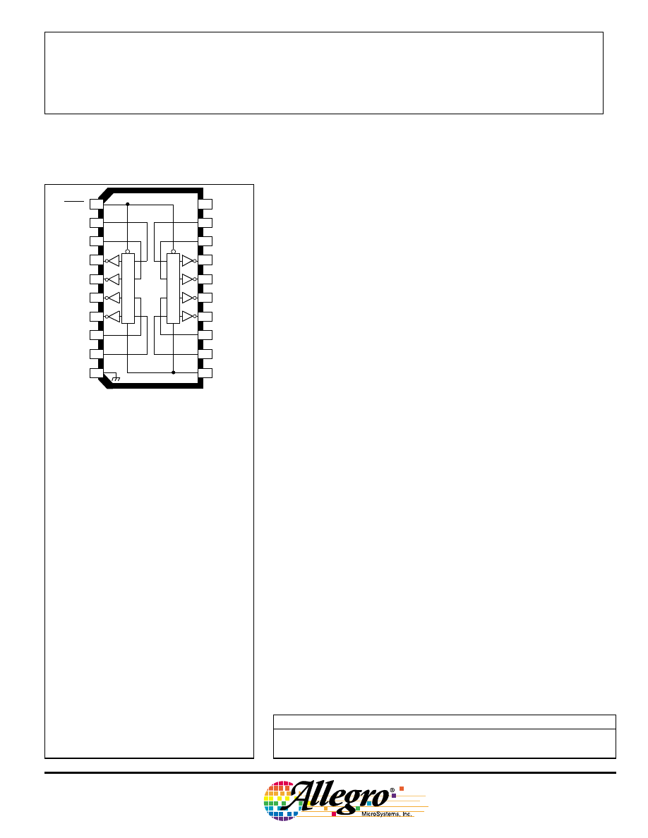
6273
Note that the A6273KA (DIP) and the A6273KLW
(SOIC) are electrically identical and share a com-
mon terminal number assignment.
1
2
3
8
9
13
14
15
16
17
19
4
5
6
7
12
18
20
IN
V
DD
GROUND
OUT
8
OUT
7
OUT
6
Dwg. PP-015-2A
OUT
1
OUT
2
OUT
3
OUT
4
OUT
5
10
11
CLEAR
LOGIC
SUPPLY
STROBE
8
IN
7
IN
6
IN
5
IN
4
IN
3
IN
2
IN
1
LATCHES
LATCHES
Always order by complete part number:
Part Number
Package
R
θθθθθ
JA
R
θθθθθ
JC
A6273KA
20-pin DIP
55
°
C/W
25
°
C/W
A6273KLW
20-lead SOIC
70
°
C/W
17
°
C/W
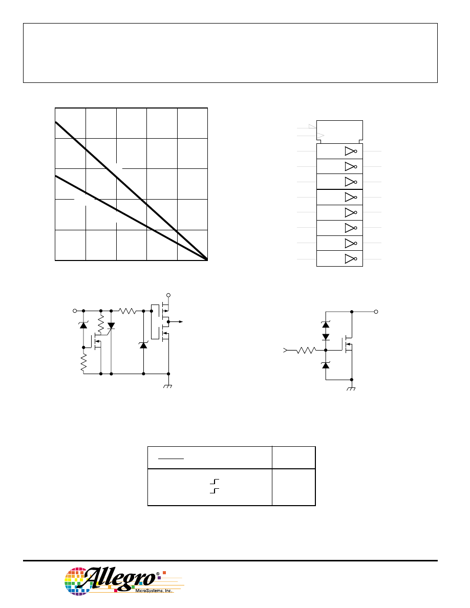
ABSOLUTE MAXIMUM RATINGS
at T
A
= 25
°
C
Output Voltage, V
O
............................. 50 V
Output Drain Current,
Continuous, I
O
....................... 250 mA*
Peak, I
OM
.............................. 750 mA*†
Peak, I
OM
..................................... 2.0 A†
Single-Pulse Avalanche Energy,
E
AS
.............................................. 75 mJ
Logic Supply Voltage, V
DD
................ 7.0 V
Input Voltage Range,
V
I
................................. -0.3 V to +7.0 V
Package Power Dissipation,
P
D
........................................ See Graph
Operating Temperature Range,
T
A
.............................. -40
°
C to +125
°
C
Storage Temperature Range,
T
S
.............................. -55
°
C to +150
°
C
* Each output, all outputs on.
† Pulse duration
≤
100
µ
s, duty cycle
≤
2%.
Caution: These CMOS devices have input
static protection (Class 3) but are still
susceptible to damage if exposed to extremely
high static electrical charges.
6273
8-BIT LATCHED
DMOS POWER DRIVER
115 Northeast Cutoff, Box 15036
Worcester, Massachusetts 01615-0036 (508) 853-5000
Copyright © 2002 Allegro MicroSystems, Inc.
LOGIC SYMBOL
C1
R
1D
4
5
6
7
14
15
16
17
1
2
11
Dwg. FP-046-1A
1D
3
1D
8
1D
9
1D
12
1D
13
1D
18
1D
19
50
75
100
125
150
2.5
0.5
0
ALLOWABLE PACKAGE POWER DISSIPATION IN WATTS
AMBIENT TEMPERATURE IN
°°°°
C
2.0
1.5
1.0
25
Dwg. GS-004B
SUFFIX 'LW', R = 90
°
C/W
θ
JA
SUFFIX 'A', R = 55
°
C/W
θ
JA
FUNCTION TABLE
Inputs
CLEAR
STROBE
IN
X
OUT
X
L
X
X
H
H
H
L
H
L
H
H
L
X
R
L = Low Logic Level
H = High Logic Level
X = Irrelevant
R = Previous State
DMOS POWER DRIVER OUTPUT
LOGIC INPUTS
IN
Dwg. EP-010-16
V
DD
Dwg. EP-063
OUT
6273
8-BIT LATCHED
DMOS POWER DRIVER
www.allegromicro.com
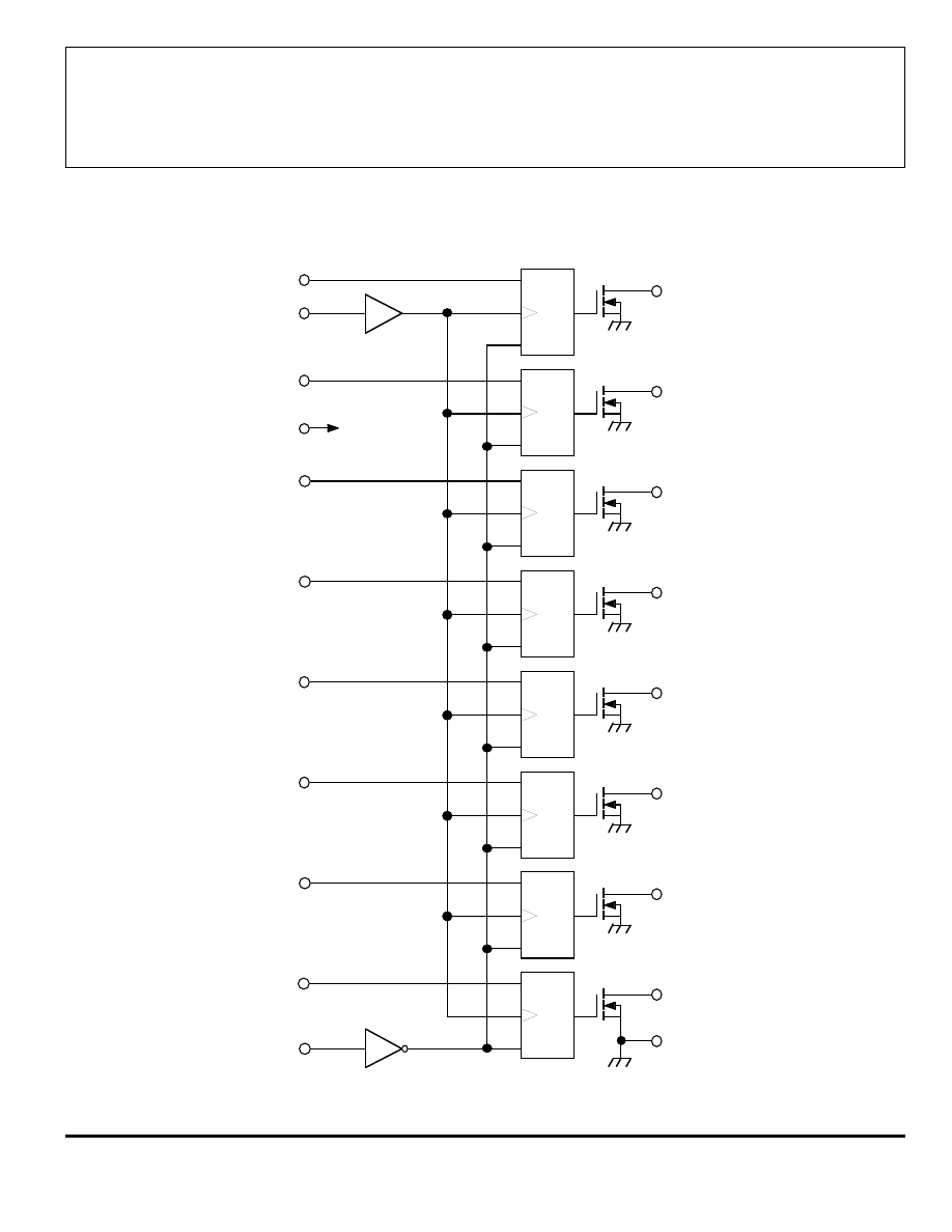
FUNCTIONAL BLOCK DIAGRAM
GROUND
Dwg. FP-016-2
CLEAR
(ACTIVE LOW)
V
DD
LOGIC
SUPPLY
OUT
1
D
C1
CLR
OUT
2
D
C1
CLR
OUT
3
D
C1
CLR
OUT
4
D
C1
CLR
OUT
5
D
C1
CLR
OUT
6
D
C1
CLR
OUT
7
D
C1
CLR
OUT
8
D
C1
CLR
1
IN
2
IN
3
IN
4
IN
5
IN
6
IN
7
IN
8
IN
STROBE
6273
8-BIT LATCHED
DMOS POWER DRIVER
115 Northeast Cutoff, Box 15036
Worcester, Massachusetts 01615-0036 (508) 853-5000
Limits
Characteristic
Symbol
Test Conditions
Min.
Typ.
Max.
Units
Logic Supply Voltage
V
DD
Operating
4.5
5.0
5.5
V
Output Breakdown
V
(BR)DSX
I
O
= 1 mA
50
—
—
V
Voltage
Off-State Output
I
DSX
V
O
= 40 V
—
0.05
1.0
µ
A
Current
V
O
= 40 V T
A
= 125
°
C
—
0.15
5.0
µ
A
Static Drain-Source
r
DS(on)
I
O
= 250 mA, V
DD
= 4.5 V
—
1.3
2.0
Ω
On-State Resistance
I
O
= 250 mA, V
DD
= 4.5 V, T
A
= 125
°
C
—
2.0
3.2
Ω
I
O
= 500 mA, V
DD
= 4.5 V (see note)
—
1.3
2.0
Ω
Nominal Output
I
O(nom)
V
DS(on)
= 0.5 V, T
A
= 85
°
C
—
250
—
mA
Current
Logic Input Current
I
IH
V
I
= V
DD
= 5.5 V
—
—
1.0
µ
A
I
IL
V
I
= 0, V
DD
= 5.5 V
—
—
-1.0
µ
A
Prop. Delay Time
t
PLH
I
O
= 250 mA, C
L
= 30 pF
—
625
—
ns
t
PHL
I
O
= 250 mA, C
L
= 30 pF
—
150
—
ns
Output Rise Time
t
r
I
O
= 250 mA, C
L
= 30 pF
—
675
—
ns
Output Fall Time
t
f
I
O
= 250 mA, C
L
= 30 pF
—
400
—
ns
Supply Current
I
DD(off)
V
DD
= 5.5 V, Outputs OFF
—
15
100
µ
A
I
DD(on)
V
DD
= 5.5 V, Outputs ON
—
150
300
µ
A
Typical Data is at V
DD
= 5 V and is for design information only.
NOTE — Pulse test, duration
≤
100
µ
s, duty cycle
≤
2%.
ELECTRICAL CHARACTERISTICS at T
A
= +25
°
C, V
DD
= 5 V, t
ir
= t
if
≤
10 ns (unless otherwise
specified).
RECOMMENDED OPERATING CONDITIONS
over operating temperature range
Logic Supply Voltage Range, V
DD
............... 4.5 V to 5.5 V
High-Level Input Voltage, V
IH
............................
≥
0.85V
DD
Low-level input voltage, V
IL
.................................
≤
0.15V
DD
6273
8-BIT LATCHED
DMOS POWER DRIVER
www.allegromicro.com
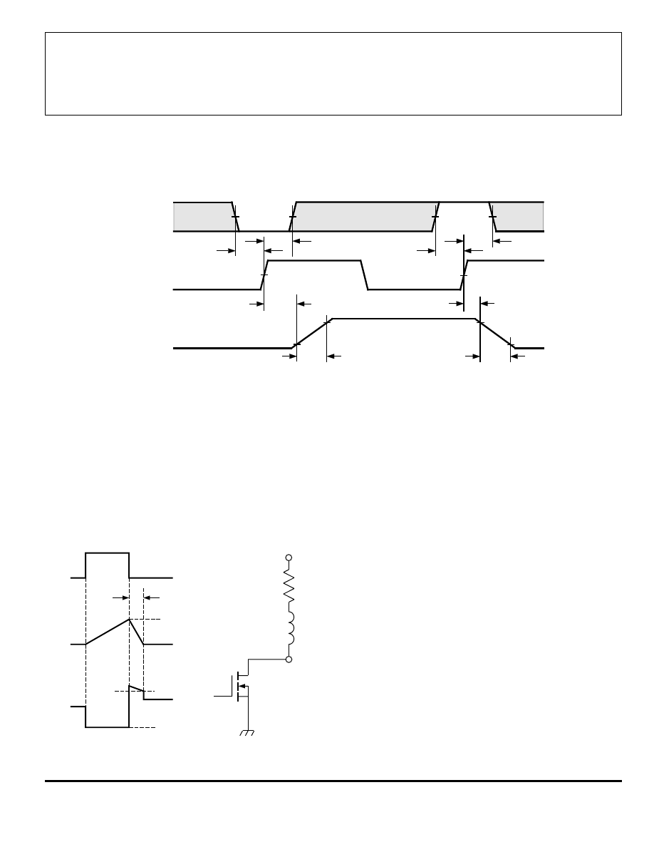
TIMING REQUIREMENTS
PHL
t
90%
f
t
50%
su(D)
t
PLH
t
50%
OUTPUTx
Dwg. WP-036-1
10%
r
t
INx
STROBE
h(D)
t
50%
su(D)
t
h(D)
t
Input Active Time Before Strobe
(Data Set-Up Time), t
su(D)
.............................................. 20 ns
Input Active Time After Strobe
(Data Hold Time), t
h(D)
................................................... 20 ns
Input Pulse Width, t
w(D)
...................................................... 40 ns
Input Logic High, V
IH
................................................
≥≥≥≥≥
0.85V
DD
Input Logic Low, V
IL
.................................................
≤≤≤≤≤
0.15V
DD
TEST CIRCUIT
Dwg. EP-066-1
OUT
INPUT
I
O
V
O
t
av
I
AS
= 1.0 A
V
(BR)DSX
V
O(ON)
0.11
Ω
100 mH
+15 V
DUT
Single-Pulse Avalanche Energy Test Circuit
and Waveforms
E
AS
= I
AS
x V
(BR)DSX
x t
AV
/2
6273
8-BIT LATCHED
DMOS POWER DRIVER
115 Northeast Cutoff, Box 15036
Worcester, Massachusetts 01615-0036 (508) 853-5000
TERMINAL DESCRIPTIONS
Terminal No.
Terminal Name
Function
1
CLEAR
When (active) LOW, all latches are reset and all outputs go HIGH (turn OFF).
2
IN
1
CMOS data input to a latch. When strobed, the output then inverts the data
input (IN
1
= HIGH, OUT
1
= LOW).
3
IN
2
CMOS data input to a latch. When strobed, the output then inverts the data
input (IN
2
= HIGH, OUT
2
= LOW).
4
OUT
1
Current-sinking, open-drain DMOS output.
5
OUT
2
Current-sinking, open-drain DMOS output.
6
OUT
3
Current-sinking, open-drain DMOS output.
7
OUT
4
Current-sinking, open-drain DMOS output.
8
IN
3
CMOS data input to a latch. When strobed, the output then inverts the data
input (IN
3
= HIGH, OUT
3
= LOW).
9
IN
4
CMOS data input to a latch. When strobed, the output then inverts the data
input (IN
4
= HIGH, OUT
4
= LOW).
10
GROUND
Reference terminal for all voltage measurements.
11
STROBE
A CMOS dynamic input to all latches. Data on each IN
x
terminal is loaded
into its associated latch on a low-to-high STROBE transition.
12
IN
5
CMOS data input to a latch. When strobed, the output then inverts the data
input (IN
5
= HIGH, OUT
5
= LOW).
13
IN
6
CMOS data input to a latch. When strobed, the output then inverts the data
input (IN
6
= HIGH, OUT
6
= LOW).
14
OUT
5
Current-sinking, open-drain DMOS output.
15
OUT
6
Current-sinking, open-drain DMOS output.
16
OUT
7
Current-sinking, open-drain DMOS output.
17
OUT
8
Current-sinking, open-drain DMOS output.
18
IN
7
CMOS data input to a latch. When strobed, the output then inverts the data
input (IN
7
= HIGH, OUT
7
= LOW).
19
IN
8
CMOS data input to a latch. When strobed, the output then inverts the data
input (IN
8
= HIGH, OUT
8
= LOW).
20
LOGIC SUPPLY
(V
DD
) The logic supply voltage (typically 5 V).
6273
8-BIT LATCHED
DMOS POWER DRIVER
www.allegromicro.com
A6273KA
Dimensions in Inches
(controlling dimensions)
Dimensions in Millimeters
(for reference only)
NOTES:1. Exact body and lead configuration at vendor’s option within limits shown.
2. Lead spacing tolerance is non-cumulative.
3. Lead thickness is measured at seating plane or below.
4. Supplied in standard sticks/tubes of 18 devices.
0.355
0.204
7.62
BSC
Dwg. MA-001-20 mm
10.92
MAX
20
1
10
7.11
6.10
5.33
MAX
1.77
1.15
0.39
MIN
0.558
0.356
2.54
BSC
0.13
MIN
3.81
2.93
11
26.92
24.89
0.014
0.008
0.300
BSC
Dwg. MA-001-20 in
0.430
MAX
20
1
10
0.280
0.240
0.210
MAX
0.070
0.045
0.015
MIN
0.022
0.014
0.100
BSC
0.005
MIN
0.150
0.115
11
1.060
0.980
6273
8-BIT LATCHED
DMOS POWER DRIVER
115 Northeast Cutoff, Box 15036
Worcester, Massachusetts 01615-0036 (508) 853-5000
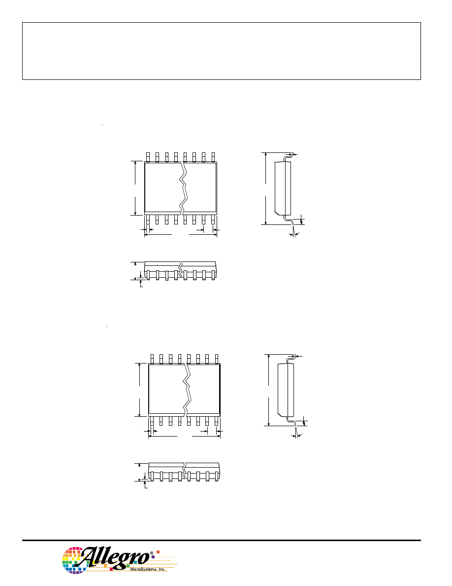
A6273KLW
Dimensions in Inches
(for reference only)
Dimensions in Millimeters
(controlling dimensions)
0
°
TO
8
°
1
2
3
0.020
0.013
0.0040
MIN.
0.0125
0.0091
0.050
0.016
Dwg. MA-008-20 in
0.050
BSC
20
11
0.2992
0.2914
0.419
0.394
0.5118
0.4961
0.0926
0.1043
0
°
TO
8
°
1
20
2
3
0.51
0.33
0.10
MIN.
Dwg. MA-008-20 mm
1.27
BSC
11
0.32
0.23
1.27
0.40
7.60
7.40
10.65
10.00
13.00
12.60
2.65
2.35
NOTES:1. Exact body and lead configuration at vendor’s option within limits shown.
2. Lead spacing tolerance is non-cumulative.
3. Supplied in standard sticks/tubes of 37 devices or add ‘TR’ to part number for tape and reel.

6273
8-BIT LATCHED
DMOS POWER DRIVER
www.allegromicro.com
The products described here are manufactured under one or more
U.S. patents or U.S. patents pending.
Allegro MicroSystems, Inc. reserves the right to make, from time to
time, such departures from the detail specifications as may be
required to permit improvements in the performance, reliability, or
manufacturability of its products. Before placing an order, the user is
cautioned to verify that the information being relied upon is current.
Allegro products are not authorized for use as critical components
in life-support devices or systems without express written approval.
The information included herein is believed to be accurate and
reliable. However, Allegro MicroSystems, Inc. assumes no responsi-
bility for its use; nor for any infringement of patents or other rights of
third parties which may result from its use.
6273
8-BIT LATCHED
DMOS POWER DRIVER
115 Northeast Cutoff, Box 15036
Worcester, Massachusetts 01615-0036 (508) 853-5000
POWER
INTERFACE DRIVERS
Function
Output Ratings*
Part Number†
SERIAL-INPUT LATCHED DRIVERS
8-Bit (saturated drivers)
-120 mA
50 V‡
5895
8-Bit
350 mA
50 V
5821
8-Bit
350 mA
80 V
5822
8-Bit
350 mA
50 V‡
5841
8-Bit
350 mA
80 V‡
5842
8-Bit (constant-current LED driver)
75 mA
17 V
6275
8-Bit (constant-current LED driver)
120 mA
24 V
6277
8-Bit (DMOS drivers)
250 mA
50 V
6595
8-Bit (DMOS drivers)
350 mA
50 V‡
6A595
8-Bit (DMOS drivers)
100 mA
50 V
6B595
10-Bit (active pull-downs)
-25 mA
60 V
5810-F and 6810
12-Bit (active pull-downs)
-25 mA
60 V
5811
16-Bit (constant-current LED driver)
75 mA
17 V
6276
20-Bit (active pull-downs)
-25 mA
60 V
5812-F and 6812
32-Bit (active pull-downs)
-25 mA
60 V
5818-F and 6818
32-Bit
100 mA
30 V
5833
32-Bit (saturated drivers)
100 mA
40 V
5832
PARALLEL-INPUT LATCHED DRIVERS
4-Bit
350 mA
50 V‡
5800
8-Bit
-25 mA
60 V
5815
8-Bit
350 mA
50 V‡
5801
8-Bit (DMOS drivers)
100 mA
50 V
6B273
8-Bit (DMOS drivers)
250 mA
50 V
6273
SPECIAL-PURPOSE DEVICES
Unipolar Stepper Motor Translator/Driver
1.25 A
50 V‡
5804
Addressable 8-Bit Decoder/DMOS Driver
250 mA
50 V
6259
Addressable 8-Bit Decoder/DMOS Driver
350 mA
50 V‡
6A259
Addressable 8-Bit Decoder/DMOS Driver
100 mA
50 V
6B259
Addressable 28-Line Decoder/Driver
450 mA
30 V
6817
*
Current is maximum specified test condition, voltage is maximum rating. See specification for sustaining voltage limits.
Negative current is defined as coming out of (sourcing) the output.
†
Complete part number includes additional characters to indicate operating temperature range and package style.
‡
Internal transient-suppression diodes included for inductive-load protection.
Wyszukiwarka
Podobne podstrony:
6273
6273
6273
6273
6273
6273
więcej podobnych podstron