Philips Semiconductors
Power Diodes
Ratings and Characteristics
Back diffused rectifier diodes
A single-diffused P-N diode with a two layer structure
cannot combine a high forward current density with a
high reverse blocking voltage.
A way out of this dilemma is provided by the three layer
structure, the so-called P-I-N diode, where ’I’ is a lightly
doped (nearly intrinsic) layer. This layer, called the base,
is sandwiched between the highly doped diffused P
+
and N
+
outer layers giving a P
+
-P-N
+
or P
+
-N-N
+
structure. Generally, the base gives the diode its high
reverse voltage, and the two diffused regions give the
high forward current rating.
Such a three layer diode can be realised using a ’back-
diffused’ structure. A lightly doped silicon wafer is given
a very long N
+
diffusion on one side, followed by a
relatively shallow P
+
diffusion on the opposite side. This
asymmetric diffusion allows better control of the
thickness of the base layer than the conventional double
diffusion method, resulting in a better trade-off between
low forward voltage and high reverse blocking voltage.
Generally, for a given silicon area, the thicker the base
layer the higher the V
R
and the lower the I
F
. Reverse
switching characteristics also determine the base
design. Fast recovery diodes usually have N-type base
regions to give ’soft’ recovery with a narrow base layer
to give fast switching.
Ultra fast rectifier diodes
Ultra fast rectifier diodes, made by epitaxial technology,
are intended for use in applications where low
conduction and switching losses are of paramount
importance and relatively low reverse blocking voltage
(V
RWM
= 150V) is required: e.g. Switched mode power
supplies operating at frequencies of about 50 kHz.
The use of epitaxial technology means that there is very
close control over the almost ideal diffusion profile and
base width giving very high carrier injection efficiencies
leading to lower conduction losses than conventional
technology permits. The well defined diffusion profile
also allows a tight control of stored minority carriers in
the base region, so that very fast turn-off times (35 ns)
can be achieved. The range of devices also has a soft
reverse recovery and a low forward recovery voltage.
Schottky-barrier rectifier diodes
Schottky-barrier rectifiers find application in low-voltage
switched-mode power supplies (e.g. a 5V output) where
they give an increase in efficiency due to the very low
forward drop, and low switching losses. Power Schottky
diodes are made by a metal-semiconductor barrier
process to minimise forward voltage losses, and being
majority carrier devices have no stored charge. They
are therefore capable of operating at extremely high
speeds. Electrical performance in forward and reverse
conduction is uniquely defined by the device’s metal-
semiconductor ’barrier height’. Philips process
minimises forward voltage drop, whilst maintaining
reverse leakage current at full rated working voltage and
T
j max
at an acceptable level.
Philips range of power schottky-barrier diodes can
withstand reverse voltage transients and have
guaranteed reverse surge capability.
Power diode ratings
A rating is a value that establishes either a limiting
capability or a limiting condition for an electronic device.
It is determined for specified values of environment and
operation, and may be stated in any suitable terms.
Limiting conditions may be either maxima or minima.
All limiting values quoted in this data handbook are
Absolute Maximum Ratings - limiting values of operating
and environmental conditions applicable to any device
of a specified type, as defined by its published data,
which should not be exceeded under the worst probable
conditions.
V
OLTAGE RATINGS
V
RSM
Non-repetitive peak reverse voltage. The
maximum allowable instantaneous reverse
voltage including all non-repetitive transients;
duration < 10 ms.
V
RRM
Repetitive peak reverse voltage. The maximum
allowable instantaneous reverse voltage
including transients which occur every cycle,
duration < 10 ms, duty cycle < 0.01.
V
RWM
Crest working reverse voltage. The maximum
allowable instantaneous reverse voltage
including transients which may be applied every
cycle excluding all repetitive and non-repetitive
transients.
V
R
Continuous reverse voltage. The maximum
allowable constant reverse voltage. Operation at
rated V
R
may be limited to junction temperatures
below T
j max
in order to prevent thermal runaway.
C
URRENT RATINGS
I
F(AV)
Average forward current. Specified for either
square or sinusoidal current waveforms at a
maximum mounting base or heatsink
temperature. The maximum average current
which may be passed through the device without
exceeding T
j max
.
I
F(RMS)
Root mean square current. The rms value of a
current waveform is the value which causes the
same dissipation as the equivalent d.c. value.
I
FRM
Repetitive peak forward current. The maximum
allowable peak forward current including
transients which occur every cycle. The junction
temperature should not exceed T
j max
during
repetitive current transients.

Philips Semiconductors
Power Diodes
Ratings and Characteristics
I
FSM
Non-repetitive forward current. The maximum
allowable peak forward current which may be
applied no more than 100 times in the life of the
device. Usually specified with reapplied V
RWM
following the surge.
I
RRM
Repetitive peak reverse current. The maximum
allowable peak reverse current including
transients which occur every cycle.
I
RSM
Non-repetitive reverse current. The maximum
allowable peak reverse current which may be
applied no more than 100 times in the life of the
device.
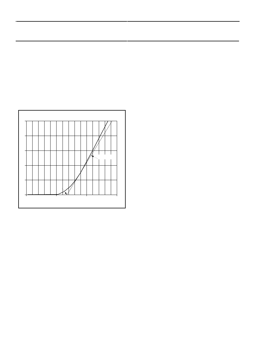
0
VF / V
50
40
30
20
10
0
0.5
1.5
1.0
IF / A
slope Rs
Vo
Figure 1: Piecewise linear approximation to diode
forward characteristic
F
ORWARD CURRENT RATINGS
The forward voltage/ current characteristic of a diode
may be approximated by a piecewise linear model as
shown in fig:1. where R
S
is the slope of the line which
passes through the rated current and V
O
is the voltage
axis intercept. The forward voltage is then
V
F
= V
O
+ I
F
.R
S
, and the instantaneous dissipation is
P
F
= V
O
.I
F
+ I
F
2
.R
S
. where I
F
is the instantaneous forward
current.
It can be shown that the average forward dissipation for
any current waveform is: P
F(AV)
= V
O
.I
F(AV)
+ I
F(RMS)
2
.R
S
,
where I
F(AV)
is the average forward current and I
F(RMS)
is
the rms value of the forward current. Graphs in the
published data show forward dissipation as a function of
average current for square or sinusoidal waveforms
over a range of duty cycles and form factors.
To ensure reliable operation, the maximum allowable
junction temperature T
j max
should not be exceeded
repetitively, either as a result of the average dissipation
in the device or as a result of high peak currents
The average junction temperature rise is the average
dissipation multiplied by the thermal resistance; R
th j-mb
or R
th j-hs
. Subtracting the junction temperature rise from
the maximum allowable junction temperature T
j max
,
gives the maximum allowable mounting base or
heatsink temperature.
The peak junction temperature rise for a rectangular
current pulse may be found by multiplying the
instantaneous power by the thermal impedance.
Analysis methods for non-rectangular pulses are
covered in the Power Semiconductor Applications
handbook.
Power diode characteristics
A characteristic is an inherent and measurable property
of a device. Such a property may be expressed as a
value for stated or recognised conditions. A
characteristic may also be a set of related values,
usually shown in graphical form.
R
EVERSE RECOVERY
When a semiconductor rectifier diode has been
conducting in the forward direction sufficiently long to
establish the steady state, there will be a charge due to
minority carriers present. Before the device can block in
the reverse direction this charge must be extracted.
This extraction takes the form of a transient reverse
current and this, together with the reverse bias voltage
results in additional power dissipation which reduces the
rectification efficiency. At sine-wave frequencies up to
about 400Hz these effects can often be ignored, but at
higher frequencies and for square waves the switching
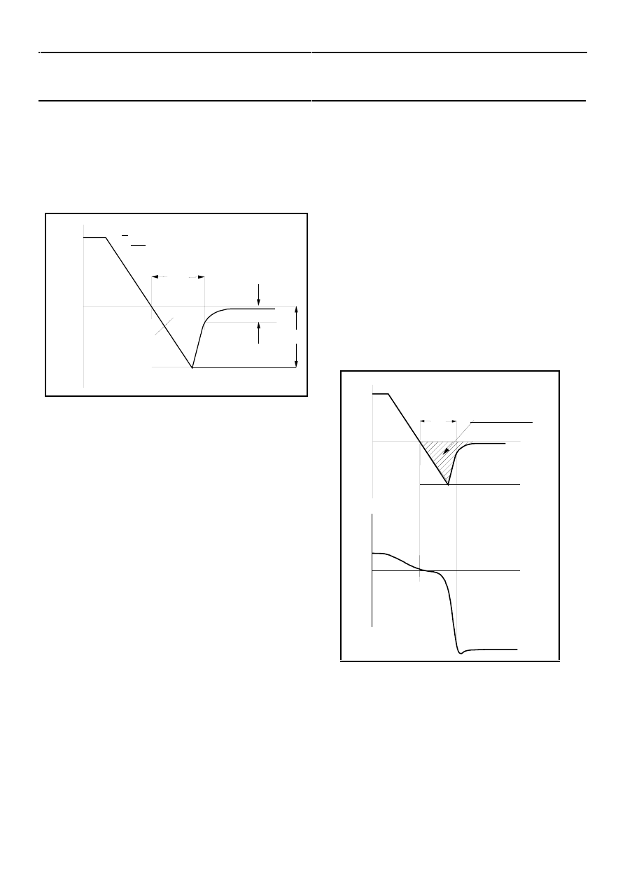
losses must be considered. The parameters of reverse
recovery are defined in fig:2.
S
TORED CHARGE
The area under the I
R
versus time curve is known as the
stored charge (Q
s
) and is normally quoted in
microcoulombs or nanocoulombs. Low stored charge
devices are preferred for fast switching applications.
R
EVERSE RECOVERY TIME
Another parameter which can be used to determine the
speed of the rectifier is the reverse recovery time (t
rr
).
This is measured from the instant the current passes
through zero (from forward to reverse) to the instant the
current recovers to either 10% or 25% of its peak
reverse value. Low reverse recovery times are
associated with low stored charge devices.
The conditions which need to be specified are:
•
Steady-state forward current (I
F
); high currents

Philips Semiconductors
Power Diodes
Ratings and Characteristics
increase recovery time.
•
Reverse bias voltage (V
R
); low reverse voltage
increases recovery time.
•
Rate of fall of anode current (dI
F
/dt); high rates of fall
reduce recovery time, but increase stored charge.
•
Junction temperature (T
j
); high temperatures
increase both recovery time and stored charge.
100%
time
dI
dt
F
I
R
I
F
I
rrm
trr
25% or 10%
Qs
Figure 2: Definition of trr, Qs and Irrm
S
OFTNESS OF RECOVERY
In many switching circuits it is not just the magnitude but
the shape of the reverse recovery characteristic that is
important. If the positive-going edge of the characteristic
has a fast rise time (as in a so-called ’snap-off’ device)
this edge may cause conducted or radiated radio
frequency interference (rfi), or it may generate high
voltages across inductors which may be in series with
the rectifier. The maximum slope of the reverse
recovery current (dI
R
/dt) is quoted as a measure of the
’softness’ of the characteristic. Low values are less
liable to give rfi problems. The measurement conditions
which need to be specified are as above.
R
EVERSE RECOVERY CURRENT
The peak value of the reverse recovery current (I
rrm
) is
an important parameter in many switched mode power
supply circuits. This is because the high transient
current produced by a diode with a high I
rrm
can be
interpreted by the circuit as a short circuit fault, which
may cause the power supply to shut down or have
apparently poor load regulation. Like the stored charge
and reverse recovery time, I
rrm
increases with increasing
temperature, so the effects sometimes only become
apparent when the equipment gets hot. I
rrm
correlates
with stored charge Q
s
. Thus choosing an Ultrafast diode
with low Q
s
usually avoids this problem.
S
WITCHING LOSSES
The product of the transient reverse current and the
reverse voltage is power dissipation, most of which
occurs whilst the reverse recovery current is decreasing
from the peak value (I
rrm
) to zero. In repetitive operation
an average power can be calculated and added to the
forward dissipation to give the total power. The peak
value of transient reverse current is known as I
rrm
. The
origin of reverse recovery losses is illustrated in fig:3.
The conditions which need to be specified are:
•
Forward current (I
F
); high currents increase
switching losses.
•
Rate of fall of anode current (dI
F
/dt); high rates of fall
increase switching losses. This is particularly
important in square-wave operation. Power losses
in sine-wave operation for a given frequency are
considerably less due to the much lower dI
F
/dt.
•
Frequency (f); high frequency means high losses.
•
Reverse bias voltage (V
R
); high reverse bias means
high losses.
•
Junction temperature (T
j
); high temperature means
high losses.
time
IR
IF
Irrm
trr
VR
VR
VF
-dIF/dt
area = Qs
Figure 3: Waveforms showing the origin of reverse
switching losses.
F
ORWARD RECOVERY
At the instant a semiconductor rectifier diode is switched
into forward conduction there are no carriers present at
the junction, hence the forward voltage drop may be
instantaneously of a high value. As the stored charge
builds up, conductivity modulation takes place and the
forward voltage rapidly falls to the steady state value.
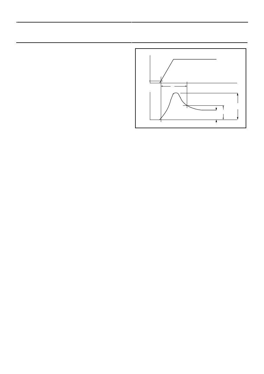
The peak value of forward voltage drop is known as the

Philips Semiconductors
Power Diodes
Ratings and Characteristics
forward recovery voltage (V
fr
). The time from the instant
the current reaches 10% of its steady-state value to the
time the forward voltage drops below a given value (
usually 5V or 2V) is known as the forward recovery time
(t
fr
). The forward recovery parameters are defined in
fig:4.
The conditions which need to be specified are:
•
Forward current (I
F
); high currents give high recovery
voltages.
•
Current pulse rise time (t
r
); short rise times give high
recovery voltages.
•
Junction temperature (T
j
); The influence of
temperature is slight.
time
time
V
F
V
fr
V
F
I
F
10%
5V / 2V
tfr
Figure 4: Definition of Vfr and tfr
Wyszukiwarka
Podobne podstrony:
Klanarchia character sheet Color1
Fireborn Scion Character Sheet
Morningstar Character Sheet
Chinese character writing Exercise sheets 2
Fading Suns Character Sheet
RATING, rachunkowość pwsz piła
Pathfinder Character Traits
Pirates Player Character Sheet
KidWorld Kid Character Sheet
Legendary Tales Character Sheet
CoC Delta Green Character Sheet
Artesia Character Sheet
A Game of Thrones Character Sheet
Danse Macabre Character Sheet
Crimes People Play Character Sheet
Fringeworthy Character Sheet
Maid Butler Character Sheet
więcej podobnych podstron