
Monolithic CMOS Power Supply for
OLED Display Driver / Controller IC
Cheung Fai Lee
SOLOMON Systech Limited
Abstract
This paper presents design considerations of a power supply IC to meet requirements for
new generations of display panel technologies, especially for OLED display panels. Major factors
include current consumption, efficiency and size. An integrated DC-DC boost converter with
current-limited minimum-off-time PFM control is designed with a standard 0.35
µm CMOS
process. Simulation results show that the efficiency can be over 80% for a load current ranging
from 1mA to 100mA for an OLED display driver/controller IC application.
I. INTRODUCTION
The portable telecommunication market has been growing rapidly, especially shifting the
focus from GSM and CDMA to wide bandwidth 3G technologies. With wider bandwidth, these
cellular phones not only support voice message, but also multimedia applications. In order to cope
with the technological change, cellular phone display technology needs to be enhanced. Beginning
with the heart of the display system, the display driver / controller plays a very important role,
which efficiently improves the display interface.
At present, Super-Twisted Nematic (STN) LCD driver IC is dominant in the display driver
market [1]. However, Organic Light-Emitting Diode (OLED) displays (Figure 1) are expected to
take off over the next decade [2]. The main advantages of OLED are simpler construction, thinner,
better viewing angle (160 degree), saturated emissive color, lower power consumption, etc. The
comparison of STN and OLED panel display technologies are shown in Table 1.
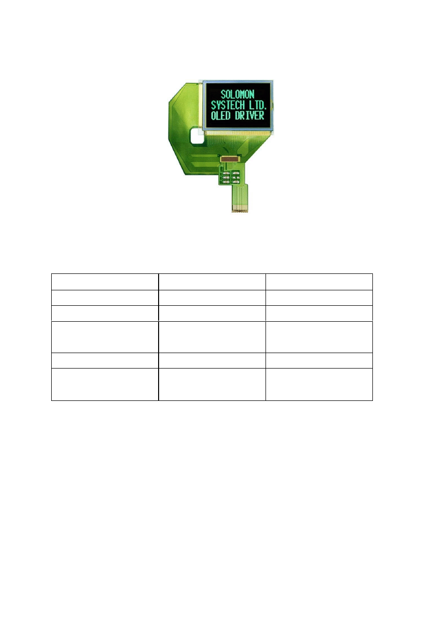
Figure 1: The OLED Driver with Controller IC
Table 1: Comparison of STN and OLED flat panel display technologies
STN
OLED
Viewing Angle
50
o
160
o
Response Time
10 ms - 100 ms
< 1 ms
Driving Method
Passive
Passive for PMOLED
Active for AMOLED
Contrast Ratio
~ 8:1
~ 100:1
Power Consumption with
Backlight
~ 100 mW
~ 10 mW
An STN LCD driver IC is needed to provide a high voltage of 10 to 18V for the STN
display panel (charging and discharging the panel), with a current consumption of the order of
100
µA. From a supply of 1.8 to 3.3V, a 3x to 6x charge pump circuit is suitable for integrated STN
LCD display IC as it requires fewer external components and no inductor. On the other hand,
OLED pixels are self-luminous. While it requires no backlighting and electrical current to supply
the OLED panels, the current consumption of an OLED driver is larger than 40mA, which also
depends on the application and the mode of operation. It is not appropriate to build a charge pump
to supply such a large loading current. Instead, inductor-based switch-mode power supply should
be considered.
II. REVIEW ON OLED DISPLAY DRIVER IC
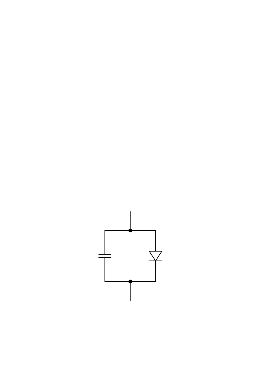
As mentioned above, OLED panels are current-controlled devices. The electrical model
and the structure of an OLED is shown in Figure 2 and Figure 3 [3], respectively, where D is the
light emitting diode and C is the parasitic capacitor of one pixel. Electrons and holes are injected
from the cathode and anode electrodes, respectively, into the electron transport layer (which can
also be the emission material) and the hole transport layer. The charge carriers then migrate under
an applied electric field to form electron-hole pairs (excitons) which then recombine, resulting in
light emission.
The maximum source current of each segment driver is around 300
µA. The total current
required is determined by the number of segments in the panel. For example, a 128 x 128 matrix
panel has 128 segments, and therefore, the maximum total current consumption from the power
supply is around 40mA. The threshold voltage of OLED panels is typically in the range of 2 to
10V. From a supply of 1.8 to 3.3V, a boost DC-DC converter is required in the OLED display
driver IC.
d
Anode
Cathode
D
C
c
I
I
Figure 2: The electrical model of OLED
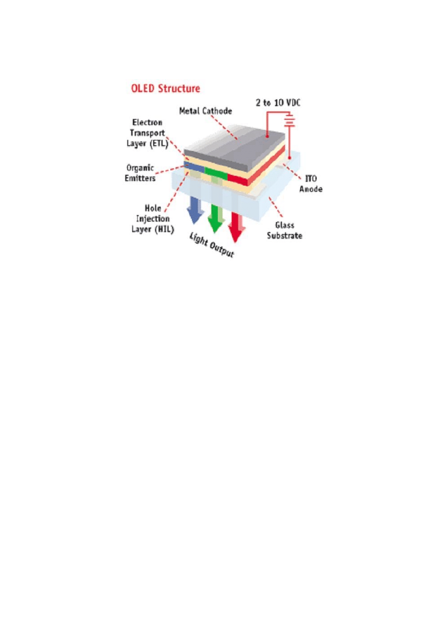
Figure 3: The structure of OLED
Since the pattern of the cellular phone display varies and the cellular phone would have
power save mode, the loading current of the OLED panel would be changing. Therefore, a good
DC-DC converter should provide high efficiency in a large range of load.
III.
CONTROL TECHNIQUES FOR OLED DRIVERS: PWM vs PFM
In terms of switching frequency, there are two control topologies for a switching converter:
the pulse width modulation (PWM) control and the pulse frequency modulation (PFM) control [4].
For a PWM converter, the output ripple voltage is usually smaller and easier to be filtered. Also,
the higher the switching frequency, the smaller the components (L and C) are needed in the power
stage. However, in the light load condition, the efficiency of the PWM control would decrease due
to switching / gate drive loss, and such power loss is dominant when comparing to conduction loss.
For the application with power save mode, the efficiency can be optimized in a PFM converter
because the switching loss would decrease with the low switching frequency at light load
condition.

As for battery-operated portable electronic devices, the two critical design issues are size
and efficiency. In a PWM control scheme, more than 2 external components are needed for
compensating the closed-loop system [4]. The number of external components in the
compensation network depends on the mode of control (current-mode control or voltage-mode
control), and the mode of operation, (DCM or CCM operations [5]). For example, 5 extra
components are required for a voltage-mode CCM boost converter. However, in the PFM control
scheme, compensation is done through the change in switching frequency, and no explicit
compensation network is needed, and therefore, fewer external components are required.
Moreover, cellular phone often operates in the standby mode, which means that the loading
current of a display panel is small. Thus, the efficiency at light load condition is very important.
Based on the above criteria, the PFM control scheme is more suitable in the OLED display driver
application.
IV.
CURRENT-LIMITED MINIMUM-OFF-TIME PULSE FREQUENCY
MODULATION
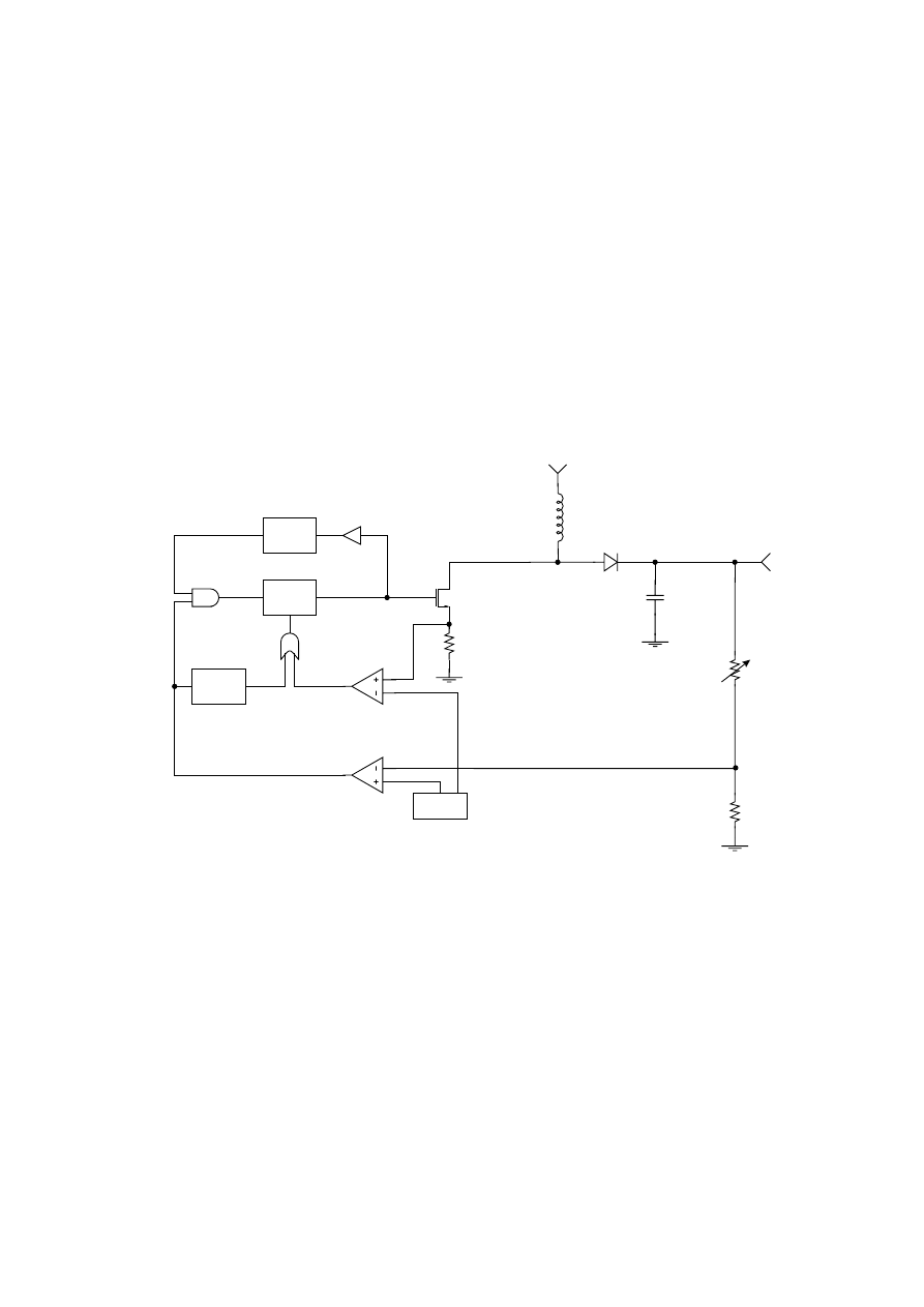
The current-limited minimum-off-time PFM scheme is widely used in the industry when
comparing to other PFM schemes, which is shown in Figure 4 [6]. The output voltage is fed back
through a voltage divider to a comparator and compared with the bandgap reference voltage. The
output of this comparator controls the trigger of a one-shot multivibrator (maximum on-time).
Another comparator looks at the peak inductor current as a voltage across a current sense resistor
in the source of the power NMOS. When the output is less than desired voltage, the SR flip-flop
turns the power NMOS on until the voltage across the current sense resistor is equal to the
reference voltage V
pk
. Then the flip-flop resets, turning off the power NMOS, the one-shot
(minimum off-time) is triggered. The power NMOS remains off for the duration of the one-shot. If
the output voltage is still out of regulation, the flip-flop will set again and the cycle repeats itself.
Besides, a variable resistor, R
fb1
, can be used to control the output voltage such that the boost
converter can provide high efficiency during the power save mode.
V. SIMULATION
RESULTS
This controller is implemented with a standard 0.35
µm CMOS process. The simulation
results are shown in Figure 5. The maximum efficiency is 87 %, which is corresponding to the
power save mode at output voltage 10 V with 10mA load current. The efficiency is 80 % at output
voltage 18 V with load current 100mA when the OLED display panels are in heavy load condition.
The results show that this control scheme provides high efficiency over a wide range of load
condition.
C
D
L
Reference
One-Shot
One-Shot
S
Flip-Flop
Q
R
Max.
On Time
One-Shot
Min.
Off Time
One-Shot
Rsense
Peak Output Current
Limiting Comparator
Output Voltage
Limiting Comparator
Rfb1
Vbat
Vout
R
V
fb2
pk
Figure 4: Current-limited minimum-off-time PFM DC-DC boost converter
VI. CONCLUSIONS
Due to high current consumption in the demand of color features in portable
telecommunication market, switch-mode power supply would be one of the best solutions for
OLED display driver ICs. And the current-limited minimum-off-time PFM controller is suitable in
this application as it does not only reduce the external components comparing to PWM control
schemes, but also provides high efficiency over a wide range of load condition.
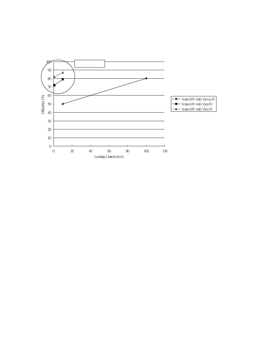
Figure 5: The efficiency at different V
out
and V
in
VII. REFERENCES
[1] SOLOMON Systech Limited, LCD Driver / Controller IC.
(http://www.solomon-systech.com)
[2] SOLOMON Systech Limited, OLED Driver / Controller IC.
(http://www.solomon-systech.com)
[3]
KODAK, Display Products: Passive Displays. (http://www.kodak.com)
[4]
R. W. Erickson and D. Maksimovic, Fundamentals of Power Electronics, Norwell Mass:
Kluwer Academic Publishers, 2001.
[5]
D. Mitchell and B. Mammano, Designing Stable Control Loops, Unitrode Power Supply
Design Seminar, 2001.
[6]
Maxim, DC-DC Converter Tutorial . (http://www.maxim-ic.com)
Power save mode
Wyszukiwarka
Podobne podstrony:
Control and Power Supply for Resistance Spot Welding (RSW)
(ebook electronics) Schematics Power Regulated Power Supply for CB & Ham Radio
Battery Inverter For Modularly Structured Pv Power Supply Systems
Adaptive fuzzy control for uninterruptible power supply with three phase PWM inverter
Adaptive fuzzy control for uninterruptible power supply with three phase PWM inverter
Layout guidlines for switching power supply
Computer Pc Power Supply Repair for print
Convert Computer ATX Power Supply to Lab Power Supply
Jvc Power Supply Description And Trouble Shooting Procedure
Innovative Solutions In Power Electronics For Variable Speed Wind Turbines
0 50V 2A LM10C, 0 50V 2A Bench power supply circuit diagrams, schematics, electronic projects
(Wydruk – ATX Switching Power Supply 13,8 V Proste zmiany w celu zwiększenia napięcia wyjściowego Ja
Ir2111 High Voltage High Speed Power Mosfet And Igbt Driver
Alarm Power Supply L78Sxx id 61 Nieznany (2)
3 2 Lab Install Power Supply
HY3010 power supply, Elektronika, Zasilacze, Zasilacz HY3010, Zasilacz HY3010, HY3010 ,INSTRUKCJA
Lekturki Power Supply Unit Lekturka
How to Modify an ATX Computer Power Supply
więcej podobnych podstron