
Western University
University of Western Ontario - Electronic Thesis and Dissertation Repository
April 2011
Control and Power Supply for Resistance Spot
Welding (RSW)
Meranda Salem
The University of Western Ontario
Supervisor
Dr. L. J. Brown
The University of Western Ontario
Follow this and additional works at:
Part of the
Controls and Control Theory Commons
This Dissertation/Thesis is brought to you for free and open access by Scholarship@Western. It has been accepted for inclusion in University of
Western Ontario - Electronic Thesis and Dissertation Repository by an authorized administrator of Scholarship@Western. For more information,
please contact
.
Recommended Citation
Salem, Meranda, "Control and Power Supply for Resistance Spot Welding (RSW)" (2011). University of Western Ontario - Electronic
Thesis and Dissertation Repository. Paper 130.

CONTROL AND POWER SUPPLY FOR RESISTANCE SPOT WELDING (RSW)
(Spine title: Control and Power Supply for RSW)
(Thesis format: Monograph)
by
Meranda Salem
Graduate Program in Electrical and Computer Engineering
A thesis submitted in partial fulfillment
of the requirements for the degree of
Doctor of Philosophy
The School of Graduate and Postdoctoral Studies
The University of Western Ontario
London, Ontario, Canada
© Meranda Salem 2011

ii
THE UNIVERSITY OF WESTERN ONTARIO
School of Graduate and Postdoctoral Studies
CERTIFICATE OF EXAMINATION
Supervisor
______________________________
Dr. L. J. Brown
Supervisory Committee
______________________________
______________________________
Examiners
______________________________
Dr. R. Eagleson
______________________________
Dr. R. Klassen
______________________________
Dr. X. Wang
______________________________
Dr. Jan P. Huissoon
The thesis by
Meranda Ahmed Salem
entitled:
Control and Power Supply for Resistance Spot Welding (RSW)
is accepted in partial fulfillment of the
requirements for the degree of
Doctor of Philosophy
_____________
______________________________________________
Date
Chair of the Thesis Examination Board: Dr. Philip J Stooke

iii
Abstract
In the automobile industry, Resistance Spot Welding (RSW) is widely used for its low cost,
high speed, simple mechanism and applicability for automation. RSW has become the
predominant means of auto body assembly, resulting in two to six thousands spot welds
performed on each manufactured car. In the North American automobile industry there are
approximately 100 billion spot welds, which are done every year.
RSW is the joining of two or more metal parts together in a localized area by resistive
heating and pressure. Small Scale RSW (SSRSW) is commonly used for medical devices and
electronic components, because the welded parts are thinner and smaller compared to
common RSW applications, such as automotive applications.
According to a study of Edison Welding Institute, 20% of the welding quality issues
are the weld schedule or power supply related. Therefore, to contribute to weld quality
improvement, the study of different weld schedules or power supplies and control schemes
needs to be improved by doing further studies in this area. Thus a novel power supply, which
can provide a testing bench for these studies, was designed and developed in 2005 by L. J.
Brown and J. Lin. This research study will focus on studying and improving weld power
supplies, weld schedules and control modes. One of the goals for this research is to improve
the consistency of weld nugget size and strength by using different control parameters, which
will be weighted geometric averages of voltage and current. These control parameters are
fed back to a Proportional Integral Derivative (PID) controller that is designed to control the
Direct Current (DC) power supply for the RSW to come up with the best control parameters
that will improve the consistency of the RSW spot welds.
Another goal for this research is it to further develop the existing DC power supply
that was designed for SSRSW by L. J. Brown, to include tip voltage measurements, and
Large Scale Resistance Spot Welding (LSRSW). This goal will lead to build additional
weld modules to construct a 6000A welder in the future.
Keywords: Resistance Spot Welding (RSW), Small Scale RSW, Large Scale RSW, DC
power Supply, PID controller, Buck Converter.

iv
Acknowledgments
I would like to thank my supervisor, Dr. Lyndon Brown of the University of Western Ontario
for his very valuable advice, guidance, and support. I am grateful to Dr. N. Zhou of the
University of Waterloo for the collaboration in the RSW project as well as Dr. Michael Kuntz
for his guidance and support during my work at University of Waterloo for my first two years
of Ph.D. I also like to appreciate my colleagues in the research group at UWO for the
discussion and support.
My special appreciation goes to all my siblings (Mohamed, Mahetab, Maissara and Melessa)
and especially to my mom Dr. Nadia Ibrahim. Without their support through out all my four
years of Ph.D., the completion of this thesis would have been impossible.
Finally, I would like to give a very special thank you to my husband Mohamed Rizk, who
came into my life the beginning of my last year of Ph.D., and was a great motivation for
getting my Ph.D. research work accomplished.

v
Table of Contents
CERTIFICATE OF EXAMINATION ........................................................................... ii
Abstract .............................................................................................................................. iii
Acknowledgments.............................................................................................................. iv
Table of Contents ................................................................................................................ v
List of Acronyms ............................................................................................................... ix
List of Tables ..................................................................................................................... xi
List of Figures ................................................................................................................... xii
List of Appendix A Figures .............................................................................................. xv
Chapter 1 ............................................................................................................................. 1
1 Introduction .................................................................................................................... 1
1.1 Research Motivation and Objective........................................................................ 2
1.1.1 Problems and Proposed Solution ................................................................ 2
1.1.1.1 RSW Power Supply...................................................................... 2
1.1.1.2 RSW Control Schemes ................................................................. 3
1.1.2 Contribution of the Thesis Work ................................................................ 5
1.2 Outline of the Thesis ............................................................................................... 7
Chapter 2 ............................................................................................................................. 8
2 Resistance Spot Welding (RSW) Background Knowledge Review .............................. 8
2.1 Welding Sequence and Classification..................................................................... 8
2.2 Resistance Spot Welding Review ......................................................................... 11
2.2.1 Heat Generation and Dynamic Resistance................................................ 11
2.2.2 Review of Existing RSW Power Supplies ................................................ 17
2.2.3 Resistance Spot Welding Sequence .......................................................... 20
2.2.4 Signals Commonly Monitored during Welding Process .......................... 24

vi
2.3 Small Scale RSW and Micro-RSW ...................................................................... 27
Chapter 3 ........................................................................................................................... 29
3 Weld Power Supply ..................................................................................................... 29
3.1 Previous Power Supply Design for SSRSW......................................................... 29
3.1.1 Power Section ........................................................................................... 31
3.1.1.1 Analysis of Powering State, Q1 off, Q2 on ................................ 34
3.1.1.2 Analysis of Freewheeling, Q1 on, Q2 off................................... 36
3.1.1.3 Selection of the Inductance L ..................................................... 37
3.2 SSRSW Power Supply Modification .................................................................... 38
3.3 SSRSW Power Supply System Requirements...................................................... 39
3.4 Electronic Circuits Designs for RSW Power Supply Modified Unit.................... 40
3.4.1 Timer Circuit............................................................................................. 40
3.4.2 PWM Analog Circuit ................................................................................ 41
3.4.3 PID Controller Analog Circuit.................................................................. 42
3.4.4 MOSFETs Driver Circuit.......................................................................... 46
3.4.5 Sensing Circuits ........................................................................................ 47
3.4.5.1 Tip Voltage Measurement .......................................................... 48
3.4.5.2 Weld Current Measurement ....................................................... 48
3.4.6 Summary of the Main Components Used in the Modified Power Supply
Unit ........................................................................................................... 49
Chapter 4 ........................................................................................................................... 51
4 Improved Consistency of Resistance Spot Welding via Power Supply Control Strategy
...................................................................................................................................... 51
4.1 RSW Control Modes............................................................................................. 52
4.1.1 Open Loop Voltage Control Mode ........................................................... 52
4.1.2 Constant Current and Tip Voltage Control Modes ................................... 53
4.2 Experimental Procedure........................................................................................ 53

vii
4.2.1 Experimental Setup................................................................................... 55
4.2.1.1 Peel Test ..................................................................................... 60
4.3 Ramp Test for Open Loop Voltage Control ......................................................... 63
4.4 PID Tuning for Constant Weld Current & Tip Voltage Control Modes .............. 66
4.5 Open Voltage, Constant Current & Constant Tip Voltage Control Modes
Comparison ........................................................................................................... 73
4.6 Conclusion ............................................................................................................ 78
Chapter 5 ........................................................................................................................... 79
5 Generic Control Mode for RSW .................................................................................. 79
5.1 Generic Power Control Mode Using Tip Voltage with Weld Current ................. 81
5.1.1 Control Strategy Design............................................................................ 81
5.1.2 Application of Strategy to Welding 0.152mm Gauge Stainless Steel....... 85
5.1.2.1 Determining Set Point for Each α............................................... 86
5.1.2.2 PID Controller Gains Tuning for Each α.................................... 87
5.1.2.3 Performing Series of Welds for Each α...................................... 88
5.1.2.4 Variance Calculation for Each α Value ...................................... 89
5.2 Generic Power Control Mode Using Nominal Voltage with Weld Current ......... 91
5.2.1 Control Strategy Design............................................................................ 92
5.2.2 Application of Strategy to Welding 0.152mm Gauge Stainless Steel....... 92
5.2.2.1 Determining Set Point for Each α............................................... 92
5.2.2.2 PID Controller Gains Tuning for Each α.................................... 93
5.2.2.3 Performing Series of Welds for Each α...................................... 94
5.2.2.4 Variance Calculations for Each α Value .................................... 95
5.3 Control Variable Variance .................................................................................... 97
5.4 Summary of the Experiments.............................................................................. 100
Chapter 6 ......................................................................................................................... 103

viii
6 Conclusion and Future Work ..................................................................................... 103
6.1 Summary of Achievements................................................................................. 103
6.2 Future Work ........................................................................................................ 104
6.3 Conclusion .......................................................................................................... 105
References....................................................................................................................... 108
Appendix A..................................................................................................................... 114
RSW Power Supply Circuit Schematics ......................................................................... 114
Curriculum Vitae ............................................................................................................ 121

ix
List of Acronyms
AC – Alternating Current
B.A.Sc. – Bachelor of Applied Science
CD – Capacitor Discharge
DC – Direct Current
DSP – DSPACE Board
LSRSW – Large Scale Resistance Spot Welding
M.A.Sc. – Masters of Applied Science
MFDC – Mid-Frequency Direct Current
MOSFET – Metal Oxide Semiconductor Field Effect Transistor
NH – Normally High Signal
NL – Normally Low Signal
Op-Amp – Operational Amplifier
PC –Personal Computer
PDF – Probability Density Function
Ph.D. – Doctor of Philosophy
PI – Proportional Integral Controller
PID – Proportional Integral Derivative Controller
PWM – Pulse Width Modulation
RSW – Resistance Spot Welding

x
SSRSW – Small Scale Resistance Spot Welding
UWO – The University of Western Ontario
α
– Current Weighting Variable

xi
List of Tables
Table
2-1: Classification of welding processes ........................................................................ 9
Table
2-2: Comparison between LSRS, SSRSW and Micro-RSW........................................ 28
Table
3-1: Technical requirements ......................................................................................... 39
Table
3-2: First and second op-amps components values ...................................................... 43
Table
3-3: PID op-amp circuit components............................................................................ 44
Table
3-4: Analog switch circuit components ........................................................................ 45
Table
3-5: Main components used in the modified power supply unit................................... 49
Table
4-1: Different duty cycles weld nugget diameters ........................................................ 65
Table
4-2: Ziegler-Nichols tuning parameters ........................................................................ 68
Table
4-3: Weld current and tip voltage transfer functions parameters.................................. 69
Table
4-4: Variance in nugget diameter.................................................................................. 74
Table
5-1: The generic control and other control modes ........................................................ 82
Table
5-2: Set points at different α values .............................................................................. 86
Table
5-3: PID controller gains values for different α values................................................. 87
Table
5-4: Mean nugget diameter for each α’s set point ........................................................ 88
Table
5-5: Set points at different α values .............................................................................. 93
Table
5-6: PID controller gains values for different α values................................................. 93
Table
5-7: Mean nugget diameter for each α’s set point ........................................................ 94

xii
List of Figures
Figure
2-1: The occurrence of resistances in electrical RSW................................................. 11
Figure
2-2: Lumped Parameter model of the secondary circuit of RSW ............................... 15
Figure
2-3: Schematic showing the change in resistance during RSW .................................. 16
Figure
2-4: Theoretical dynamic resistance curve .................................................................. 16
Figure
2-5: Sketch of current waveforms of CD, DC and AC power supplies ...................... 19
Figure
2-6: The procedure of RSW ........................................................................................ 21
Figure
2-7: Schematic of a typical RSW monitoring and control system .............................. 23
Figure
3-1: SSRSW system
[42]............................................................................................. 29
Figure
3-2: System block diagram
[42] .................................................................................. 30
Figure
3-3: Actual experimental setup
[42] ............................................................................ 31
Figure
3-4: Power section
[42] ............................................................................................... 32
Figure
3-5: Steady state equivalent circuits
[42] .................................................................... 34
Figure
3-6: Steady state waveforms
[42] ................................................................................ 36
Figure
3-7: Load current profile within a switching period
[42] ............................................ 37
Figure
3-8: Timer circuit output signals graph ....................................................................... 41
Figure
3-9: PWM & timer NH signal graph ........................................................................... 42
Figure
3-10: PID analog circuit .............................................................................................. 46
Figure
3-11: Analog switches timing graph............................................................................ 46
Figure
3-12: Driver gates G1, G2 & PWM signals
[42]......................................................... 47

xiii
Figure
3-13: Tip voltage (a) diagram
[42] & (b) circuit schematic ........................................ 48
Figure
3-14: Sensing circuit for weld current
[42],
[44]......................................................... 49
Figure
3-15: RSW power supply modified unit...................................................................... 50
Figure
4-1: Block diagram of open loop voltage control mode.............................................. 53
Figure
4-2: Probability density function for determining number of experiments................. 55
Figure
4-3: Typical dynamic resistance for constant voltage and current control modes ...... 56
Figure
4-4: Block diagram of experimental set-up ................................................................. 56
Figure
4-5: Welder head, force adjustable down-top & foot pedal ........................................ 57
Figure
4-6: Electrode force ..................................................................................................... 58
Figure
4-7: Adjusted electrode force ...................................................................................... 59
Figure
4-8: Peel test sample.................................................................................................... 60
Figure
4-9: Peel test for measuring nugget diameter .............................................................. 60
Figure
4-10: Schematic showing joint failure modes during peel test.................................... 61
Figure
4-11: Nugget diameter picture for one of the welding samples .................................. 62
Figure
4-12: Weld current ramp from 30% to 80% duty cycles............................................. 64
Figure
4-13: Quarter decay ratio............................................................................................. 66
Figure
4-14: Ziegler-Nichols S shape curve ........................................................................... 67
Figure
4-15: Tip voltage step test ........................................................................................... 70
Figure
4-16: Weld current step test......................................................................................... 71
Figure
4-17: PID Simulink model........................................................................................... 71

xiv
Figure
4-18: PID controller tuning for constant voltage control mode .................................. 72
Figure
4-19: PID controller tuning for constant current control mode ................................... 73
Figure
4-20: Variance comparison in nugget diameter........................................................... 75
Figure
4-21: Open Loop Voltage Control Histogram............................................................. 76
Figure
4-22: Constant Current Control Histogram ................................................................. 77
Figure
4-23: Constant Tip Voltage Control Histogram .......................................................... 78
Figure
5-1: Generic power control mode................................................................................ 79
Figure
5-2: Experimental results for constant tip voltage control mode (α=0) ...................... 83
Figure
5-3: Experimental results for constant power control mode (α=1/2) .......................... 84
Figure
5-4: Experimental results for constant weld current control mode (α=1) ................... 85
Figure
5-5: Variance comparison in nugget diameter using tip voltage ................................. 89
Figure
5-6: Variance comparison in nugget diameter using tip voltage moving average ...... 91
Figure
5-7: Nominal voltage generic power control mode..................................................... 92
Figure
5-8; Variance comparison in nugget diameter using nominal voltage ........................ 96
Figure
5-9: Variance comparison in nugget diameter using nominal voltage moving average
................................................................................................................................................. 97
Figure
5-10: Normalized variance comparison in control variables for each α value using tip
voltage..................................................................................................................................... 99
Figure
5-11: Normalized variance comparison in control variables for each α value using
nominal voltage..................................................................................................................... 100

xv
List of Appendix A Figures
Figure A- 1: Timer circuit schematic.................................................................................... 114
Figure A- 2: PID circuit schematic ....................................................................................... 115
Figure A- 3: PWM circuit schematic .................................................................................... 116
Figure A- 4: MOSFETs driver circuit schematic.................................................................. 117
Figure A- 5: Sensors circuit schematic ................................................................................. 118
Figure A- 6: Capacitor circuit schematic .............................................................................. 119
Figure A- 7: Power supply power components circuit schematic ........................................ 120

1
Chapter 1
1
Introduction
Resistance spot welding (RSW) is one of the key metal joining techniques for high
volume production in the automotive, biomedical and electronics industry. RSW is a
process in which faying surfaces are joined in one or more spots by the heat generated by
resistance to the flow of electric current through workpieces that are held together under
force by electrodes. A short time pulse of high-amperage current heats the contacting
surfaces in the region of current concentration. When the flow of current ceases, the
electrode force is maintained while the weld metal rapidly cools and solidifies. The
electrodes are retracted after each weld, which usually is completed in a fraction of a
second. Large-Scale Resistance Spot Welding (LSRSW) has become the predominant
means of auto body assembly, with an average of two to six thousands spot welds
performed on each manufactured car leading to 100 billion spot welds per year in the
North America automobile industry. On the other hand, for increasing application of very
thin metal sheets in manufacturing electronic components and devices, Small-Scale
Resistance Spot Welding (SSRSW) is attracting more and more researchers’ attention
[1].
Weld quality and weld power supplies are the center of all aspects of welding in
general and more specifically in the automobile industry. Hence, a material, before it is
used in production, needs to be qualified as weldable; namely, that using standard
welding equipment and schedules would yield welds of sufficient size and strength.
RSW differs from some other forms of welding in that no extra material is used, such as
filler rod in arc welding; hence it is not complicated by the addition of extra material.
However, the melting process is entirely contained within the workpieces, thus
observation and measurement are severely constrained and there are no universally
accepted standards of weld quality. Therefore, for the sole purpose of assuring the
quality of the spot weld, the primary objective of spot welding research has been to
monitor and control the process
[2],
[3] especially in the automobile industry. However,
due to the fact that industrial welder's power supplies are not flexible for RSW

2
monitoring and control research, less work has been done to improve the consistency for
LSRSW.
1.1 Research Motivation and Objective
1.1.1
Problems and Proposed Solution
The main two problems for improving RSW consistency process are the power supply
design that the controller parameters will be applied to, and choosing the right control
parameters that will maximize the consistency of RSW process.
1.1.1.1
RSW Power Supply
There are four basic types of power supplies used in Resistance Spot Welding
[4].
• Direct Energy (AC) Power Supply, which provides alternating current (AC) of the
same frequency as the input power line;
• Capacitor Discharge (CD) Power Supply, which provides the weld current by
discharging the energy stored in a capacitor bank;
• Mid Frequency Inverter (MFDC) Power Supply, which controls the weld energy by
means of mid frequency switching technology;
• Direct Current (Linear DC) Power Supply, which provides pure DC weld current
through power transistors working in their linear range.
Most LSRSW systems use direct energy (AC) power supplies [5]. Downsized welder
power supplies are used for SSRSW systems. Most SSRSW applications use “closed
loop” controlled power supplies including constant current, voltage and power control
modes and providing faster speed and smaller time intervals (1 millisecond), such as
downsized MFDC power supplies and Linear DC power supplies. Nevertheless, some
SSRSW applications also use CD power supplies, which use “open loop” control scheme.
CD power supplies could be the most common power supplies used with SSRSW
machines. The main features of these power supplies are described in the following
chapter. A linear DC power supply is not scalable and expensive, while direct AC and

3
CD power supplies have limited control. Direct AC power supplies can only be adjusted
every half cycle, (and due to transformer saturation considerations practically only every
cycle) which gives very limited opportunities for adjusting their output. Further even with
mid-frequency power, commercially available power supplies generally do not allow you
to change power settings during the weld. Therefore, these power supplies are expensive
and not flexible to be used as a test bench for performing different research studies to
improve weld power supplies and control schemes. Therefore a novel power supply,
which can provide a testing bench for these studies, was designed and developed in 2005
by L. J. Brown and J. Lin [6], [7], [8]. The first goal of this research was to further
develop and improve this power supply to implement this research work in improving
weld power supplies and control modes for LSRSW.
1.1.1.2
RSW Control Schemes
In previous research, the electrical current or voltage [9], clamping force [10] and
dynamic resistance [11] signals have been indicated as being the most used in monitoring
and control systems to evaluate weld quality. Based on either information obtained from
the monitoring and/or modeling, control algorithms have to be developed to control the
process for assuring quality welds. However, market penetration of these algorithms has
been poor, often because the algorithms are not robust for real conditions on a shop floor.
The approach presented here has advantages of simplicity and requires little modification
of existing practice.
Quite a few papers have been published for RSW weld quality with different
control schemes [12], [13], [14] including open loop control, constant current control and
constant power control.
Traditional control of the welding operation is open-loop and weld engineers
preselect appropriate values for timing parameters, including firing angles of Silicon
Controlled Rectifiers (SCR). Initial improvement included adjusting the timing
parameters to account for line voltage variations [15].
The resistances across the workpieces are extremely low, often in the 10s of

4
µohms for LSRSW and in the few milliohm for SSRSW. This is of the same order as
both the source resistance of power supply and weld cables. Further any movement of
the weld cable can have significant impact on its inductance as this is a function of loop
area. Thus control of the voltage at the power supply does not provide good control of
the power delivered to the weld, and consistency is reduced when the generated heat is
arbitrarily varied. Using active feedback to regulate the current supplied by the weld
power supply reduces many of these sources of variability. Thus the demand for highly
improved welding consistency has led to switching from open loop control to current
control by using feedback to regulate a constant current that can reduce heating variance
during the formation of a weld [16].
Nevertheless, in the constant current control method for resistance spot welding,
the generated heat is varied due to the change of the specimen resistance. Similar to the
power supply voltage, the welding current itself does not represent the input heat either.
In order to determine the heat input to a weld, both voltage and current must be
measured. Therefore, controllers based on the so-called constant power control algorithm
have been developed and are now commercially available with small-scale resistance
spot welders. As a result, the generated heat can be kept constant, resulting in fewer
expulsions (expulsion is a characteristic of over-welding where molten metal is expelled
from the weld nugget as a violent shower of sparks) [17]. However, the constant power
controls are still not perfect. Generally the voltage is measured at the power supply
instead of at the weld. In practice, as discussed later, it is not practically possible at this
point in time to measure voltage at the weld with most LSRSW. Furthermore, because
some of the current passes through adjacent welds and outside of the electrodes, the
measured current is larger than the effective current. Thus some other measure of voltage
and current should be able to lead to more consistent welds.
The geometric mean in mathematics is defined as a type of mean or average,
which indicates the central tendency or typical value of a set of numbers. It is generally
understood that geometric means are often more natural than arithmetic means, when
dealing with numbers with different scales. The geometric mean of n numbers is formed

5
by the nth root of their product. Thus the geometric mean of voltage and current is
1
2
(
)
VI
,
i.e., the square root of the power. A weighted geometric mean of variables V and I would
be given by
1
V
I
α α
−
where 0 ≤ α ≤ 1 is the weighting. A research study that was done at
UWO by J. Bai et al [18] proposed that any weighted geometric mean of voltage and
current is a viable control variable and that this approach unifies the existing constant
current
1
α
= , constant power
1
2
α
=
and constant voltage
0
α
= strategies. This research
was done to investigate the selection of the control variable proposed in a generic power
control mode to achieve the most consistent welds experimentally and through
optimization of uncertainty models. This provides a new tool for the weld engineer to
maximize the quality of their welding processes. For welding 0.152mm gauge stainless
steel, it was found a 40% weighting on the voltage produced the most consistent weld
nugget diameter, and with this control parameter, a 60% improvement in variance in weld
nugget size versus constant current control was achieved.
This research was done using a nominal voltage with weld current as a feedback
to a Proportional Integral (PI) controller. However, while successfully demonstrating the
potential of this approach, this research was compromised by relatively poor performance
of the control algorithms. Visual inspection of the control signal did not lend confidence
to the controller having effectively achieved control of the desired mean of voltage and
current. The second goal of this thesis is to repeat this research study, first by using
actual tip-voltage instead of nominal voltage with weld current as a feedback to a PID
controller instead of PI controller, and then by using the nominal voltage again with the
weld current as a feedback to the PID controller. To demonstrate this strategy, it will be
applied to the welding of 0.152mm thick stainless steel. The results for using the tip
voltage as feedback will be compared with the results for using the nominal voltage, to
see how much improvement was achieved in the consistency for RSW.
1.1.2
Contribution of the Thesis Work
The aim for this thesis is to present a new modification for the previously designed DC
power supply in 2005 by L. J. Brown
[6],
[7],
[8] as well as a new control strategy to

6
improve the consistency of resistance spot welding for every spot weld.
This thesis presents a DC power supply that can provide a testing bench for these
studies. This power supply can use tip voltage & current measurements to apply different
control schemes using a PID controller to improve the consistency of the RSW process.
Moreover, the structure of this power supply naturally allows it to scale from SSRSW to
LSRSW for future research on improving automotive RSW consistency.
The modification that was done for the novel DC power supply was in the
controller section by replacing the 8-bit microcontroller, PIC 16F73 from Microchip, Inc.
with the option of using an externally supplied pulse width modulated (PWM) signal, or
generating its own PWM signal from an analog PWM chip. The set point for the analog
PWM chip can be generated internally as a fixed value, from a built-in analog PID
controller or from an external analog signal. Normally we generate the external PWM
signal from a DSPACE control board (DSP) with a controller implemented with Open
Desk software. In total there are 5 operating modes:
1)
External PWM signal
2)
External analog reference for the PID controller
3)
External analog duty cycle (D)
4)
Internally generated duty cycle (D)
5)
Internally generated reference with PID controller
Both the built-in controller and the controller implemented on the control board
have the option of using tip voltage or welding current as feedback variables. The full
use of these control variables for the control board will be discussed later in the following
chapters. This configuration gives the flexibility to quickly test advanced,
computationally intensive control algorithms on the dedicated control board and then test
the implementation on extremely low cost commercially viable hardware. Moreover, the
combination of the inductor based output filtering and the ability to control the duty cycle
via externally generated analog value or PWM signal allows the units to be easily

7
connected in parallel. This allows research to be conducted at current levels (~10kA)
necessary for the standard gauges used in the automotive industry.
Finally, the modified DC power supply could be used in the future to find the
optimum control parameter to improve the consistency for LSRSW, using tip-voltage
with weld current measurements as feedback to a PID controller. The PID controller was
designed to use any weighted geometric mean of the tip-voltage and weld current as a
control variable, since changing control variable affects the consistency of welding
process. Hence there should be one specific weighted mean of voltage and current that
can lead to the least variance in the weld process. This provides a new tool for the weld
engineer to maximize the quality of their welding processes.
1.2
Outline of the Thesis
The thesis is organized as follows:
Chapter 1 gives a brief introduction of the resistance spot welding (RSW) and
presents the contribution and the structure of this thesis. In
Chapter 2, a general review
of welding process is proposed, the working principle of the RSW and the existing power
supplies are described.
Chapter 3 presents the modification that was implemented for the
novel DC power supply that was previously designed by L. J. Brown in 2005
[6],
[7],
[8].
Chapter 4 presents the second part of my Ph.D. research work, which is the improved
consistency of resistance spot welding via power supply control strategy. In this chapter,
a PID controller is designed and three different control modes are discussed and
implemented for the welding process. After studying these three control modes, the
application of this new strategy to welding 0.152mm gauge stainless steel and the
experimental procedure are presented as well. Chapter 5 explains the generic control
mode for RSW as well as the experimental analysis for it. The welding quality under
different control variable has been analyzed based on the experimental results. The
experimental results demonstrate the feasibility of the proposed control strategy and the
stability of the control modes has been analyzed. Finally,
Chapter 6 concludes the
achievements of this thesis and provides suggestions for future work.

8
Chapter 2
2
Resistance Spot Welding (RSW) Background
Knowledge Review
Some background knowledge is introduced in this chapter, in order to provide a clear
picture on resistance spot welding. General principles of the welding process are
presented in the first section, to explain the application of welding, and its classification.
Next, the resistance spot-welding procedure, existing power supplies and typical welding
parameter monitoring are described. Finally, the applications of small-scale and micro-
scale resistance spot welding are reviewed.
2.1 Welding Sequence and Classification
Welding is a fabrication process that joins materials, usually metals or thermoplastics, by
causing coalescence. This is often done by melting the workpieces and adding a filler
material to form a pool of molten material (the weld puddle) that cools to become a
strong joint, with pressure sometimes used in conjunction with heat, or by itself, to
produce the weld. Many different energy sources can be used for welding, including a
gas flame, an electric arc, a laser, an electron beam, friction, and ultrasound.
The American Welding Society definition for a welding process is ”a materials
joining process which produces coalescence of materials by heating them to suitable
temperatures with or without the application of pressure or by the application of pressure
alone and with or without the use of filler material”
[56],
[57]. Welding processes have
been classified based on the mode of energy transfer and the influence of capillary
attraction in effecting distribution of filler metal in the joint as the two main factors.
Capillary attraction distinguishes the welding processes grouped under ”Brazing”,
”Soldering”, ”Arc Welding”, ”Gas Welding”, ”Resistance Welding”, ”Solid State
Welding”, and ”Other Processes” [19]. Table
2-1 lists the common welding process in
their official groupings. This table also shows the letter designation for each process.
The letter designation assigned to the process can be used for identification on drawings,
tables, etc.

9
The selection of a specific welding process depends upon many factors, such as
the geometric shape, material, size, thickness, costs, portability, and skills needed, etc.
Resistance spot welding is widely and commercially used in industries like automobile,
cabinet, aerospace, appliance, etc [8]. In this thesis, resistance spot welding was studied.
Resistance welding is a joining process belonging to the pressure-welding sector,
and it is extensively used for the mass production assembly of the all-steel body of cars
and its component sheet metal parts. Its wide adaptation has been brought about by its
technical advantages and the low cost. There are a number of resistance welding
processes as shown in Table
2-1. In addition, RSW is the primary sheet metal welding
process in the manufacture of automotive assemblies.
Table
2-1: Classification of welding processes
Group
Welding Process
Letter Designation
Carbon Arc
CAW
Flux Cored Arc
FCAW
Gas Metal Arc
GMAW
Gas Tungsten Arc
GTAW
Plasma Arc
PAW
Arc Welding
Shielded Metal Arc
SMAW
Diffusion Brazing
DFB
Dip Brazing
DB
Furnace Brazing
FB
Induction Brazing
IB
Resistance Brazing
RB
Brazing
Torch Brazing
TB
Oxyacetylene Welding
OAW
Oxyhydrogen Welding
OHW
Oxyfuel Gas Welding
Pressure Gas Welding
PGW
Flash Welding
FW
High Frequency Resistance
HFRW
Percussion Welding
PEW
Projection Welding
PRW
Resistance-Seam Welding
PSEW
Resistance-Spot Welding
RSW
Resistance Welding
Upset Welding
UW

10
Cold Welding
CW
Diffusion Welding
DFW
Explosion Welding
EXW
Friction Welding
FRW
Hot Pressure Welding
HPW
Solid State Welding
Ultrasonic Welding
USW
Dip Soldering
DS
Furnace Soldering
FS
Induction Soldering
IS
Infrared Soldering
IRS
Iron Soldering
INS
Soldering
Resistance Soldering
RS
Spot welding is used throughout the industry for two main reasons: first, because
it is the strongest and generally reliable method of joining two pieces of metal; and
second, because of the total absence of panel distortion through the welding [20].
Besides during the welding process, there is no extra material used, which is different
from other welding process, hence it is not complicated by the addition of extra material.
Moreover, since car body design demands careful choice of the sheet metal, tensile
strength and ductility which are good in mild steel, are vital to the ability to absorb the
impact energy, therefore resistance spot welds are widely used in the automotive sector.
Furthermore, spot welding is a typical technology of body-in-white fabrication in the
automotive industry, and as such it has the benefit of being a well-known extensively
proven technology with which the industry is highly familiar and has considerable
experience. One of the biggest advantages of spot welding is having extremely low cost,
less than 1 cent per weld in consumables. Other main advantages of spot welding include
high operating speeds and suitability for automation or robotization and inclusion in high-
production assembly lines together with other fabricating operations. Another common
application of RSW is the attachment of braces, brackets, pads, or clips to formed sheet-
metal parts such as cases, covers, bases, or trays. With automatic control of current,
timing and electrode force, sound spot welds can be produced reasonably and
consistently at high production rates and low unit labour costs using semiskilled
operators. RSW process is especially favoured in manufacturing since it involves no
11
direct consumable besides electricity. A resistance spot weld typically requires15kJ .
Since electricity is typically priced in the pennies per
.
kw hour
, this involves tiny fractions
of a cent as compared to the substantially higher cost of screws or rivets.
2.2
Resistance Spot Welding Review
In the spot welding process, two overlapped or stacked stamped components are welded
together as a result of the resistance heating caused by the passage of electric current.
This resistance heating is provided by the workpieces as they are held together under
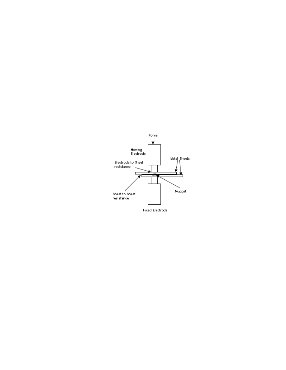
pressure between two electrodes as shown in Figure
2-1
[21].
Figure
2-1: The occurrence of resistances in electrical RSW
The copper alloy electrodes are used to apply pressure and convey the electrical
current through the workpiece during the formation of nugget. In the spot welding
process, a weld nugget will start to form after sufficient energy has been put into the weld
zone to raise the material to the solidus-liquidus temperature of the materials to be
bonded and hence to begin the formation of a melted weld pool. The magnitude and
duration of the current and the resistance of the workpieces determine the size of the
formed nugget.
2.2.1
Heat Generation and Dynamic Resistance
The heat needed to create the coherence is generated by applying an electric current

12
through the stack-up of sheets between the electrodes. Therefore, the formation of a
welded joint strongly depends on the electrical and thermal properties of the sheet and
coating materials. As a weld’s formation can be linked to the electrical and thermal
processes of welding, controlling the electrical and thermal parameters is a common
practice. The general expression of heat generated in an electric circuit can be expressed
as
2
2
/
t
t
Q
I Rdt
V
Rdt
V Idt
=
=
=
∫
∫
∫
(2.1)
where, Q is the heat generated in the workpieces, I is the welding current, V
t
is the
voltage at the weld tips and R is the electrical resistance seen at the weld head. Since it is
well know that the resistance, and possibly the current and voltage, vary with time, the
above expression is expressed as an integral over time.
In fact, the resistance in the circuit is composed of many sources, which
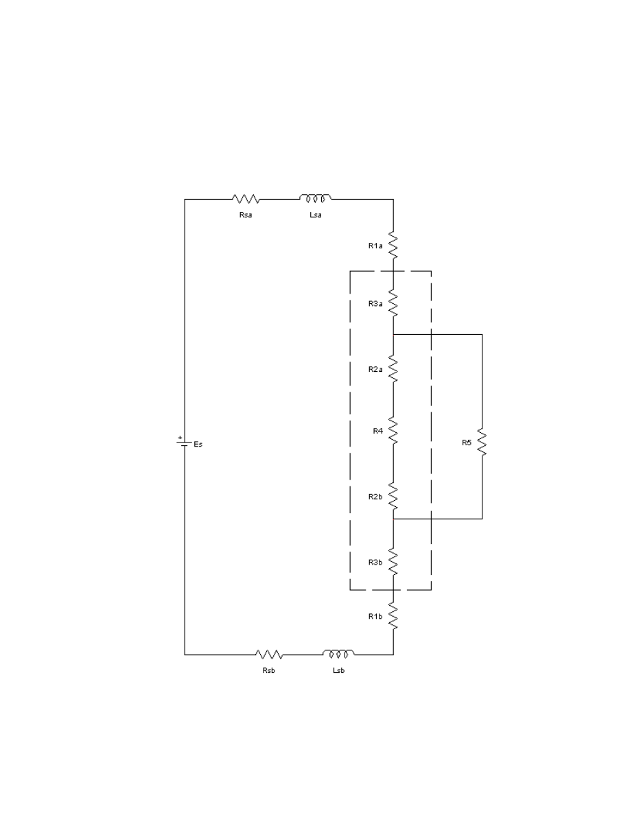
contribute in various degrees to the production of the weld. Figure
2-2 shows a common
lumped parameter model of the secondary circuit for RSW systems. As shown in the
figure, the model consists of a voltage source Es, resistances of the cables Rsa and Rsb,
inductances Lsa and Lsb, bulk resistances of the upper/lower electrodes R1a and R1b,
shunt resistance R5 that represents the resistance of current flowing around the weld spot
and through adjacent welds as well as the load dynamic resistance.
The load resistance is the key component in this circuit, which is a function of the
weld force, the materials to be used and temperature during welding. It consists of the
following components as shown in (Figure
2-2):
• Bulk resistances of the upper/lower part joints R2a, R2b,
• Contact resistances between the upper/lower electrode and workpiece R3a as well
as R3b,
• Contact resistance between the two workpieces R4.

13
The bulk resistance is sensitive to temperature and independent of pressure. For all
metals, the bulk resistance increases with temperature. The bulk resistance is a function
of temperature via two separate processes. Resistivity is an increasing function of
temperature. In addition as temperature rises, the metal expands, causing an increase in
resistance as resistance is proportional to the distance the current has to travel. Therefore,
the bulk resistance is an important factor for welding quality in a weld of long duration.
The contact resistance is a strong function of pressure or force, and also affected by the
environment of the contact surface. It will change dramatically as melting commences;
therefore the contact resistance is the most important parameter in the beginning few
milliseconds in the welding process.
The load resistance attributed to the contributions of the contact resistance and bulk
resistance is thus not constant during the process, leading to variations in the rate of
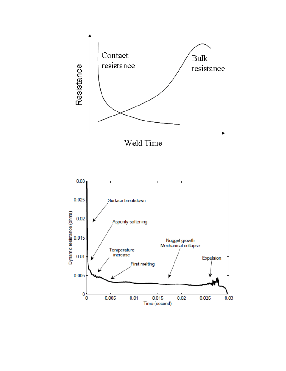
heating during the weld. Figure
2-3 is a sketch, which shows the trends in changes in
resistance during resistance spot welding [22].
Based on the above analysis, the following interpretation for the typical shape of the
dynamic resistance curve is given. With reference to Figure
2-4, the stages of spot weld
formation can be described as follows [23]:
• StageI: The workpieces are brought into contact under the pressure provided by
the electrode force. Voltage is applied between the electrodes causing current to
flow at the contact points. The resistance between electrodes at this point is equal
to the sum of the bulk resistance of the two workpieces, the two electrode-to-work
contact resistance, and the work-to-work contact resistance. Under normal
conditions, the initial contact resistance will be very high. Therefore, the initial
generation of heat will be concentrated at all surfaces, especially at the work-to-
work contacts. This heat will cause the surface contaminants to break down
resulting in a very sharp drop in resistance.
• StageII: Immediately after the breakdown of surface contaminants, metal-to-metal
contact exists. At a microscopic level, the apparently smooth metallic faces are
actually uneven surfaces composed of hills and valleys. Thus the continuous

14
contact of both the electrode to workpiece interfaces and the workpiece to
workpiece interface(s) will actually be composed of many disjoint contacts at
asperities reducing the contact area to a tiny fraction of the electrode face. This
results in a relatively large interface resistance. Heating then is concentrated at the
work-to-work surface, and temperature in this region and in the bulk materials will
increase. As heating progresses, the asperities soften and the contact area
increases thus causing resistance to decrease. At the same time increasing
temperature result in increasing resistivity, thus providing an opposite effect.
Eventually, the increase in contact area will be overcome by the increasing
temperature effect, and the total resistance will begin to rise.
• StageIII: During this period, the increase in resistivity resulting from increasing
temperature dominates the resistance curve.
• StageIV: The bulk of the workpieces continue to increase in temperature, thus
causing resistivity and resistance to increase. But the heat being generated also
cause additional melting to occur at the surfaces, increasing the size of the molten
region and the cross-sectional area available for current flow that causes a
resistance decrease. Also increased softening will result in some mechanical
collapse, shortening the path for current flow and decreasing resistance. Therefore
the resistance starts to decrease.
• StageV: The growth of the molten nugget and mechanical collapse continue to
cause resistance to decrease. Expulsion will occur if the nugget grows to a size
such that the surrounding solid metal under the compressive electrode force can no
longer contain it.
This series of events offers a consistent interpretation of the shape of the dynamic
resistance curves observed for the spot welding process. Current level, electrode force,
and materials being welded are the variables expected to cause significant variation in the
shape.
15
It should be noted that with different control modes for the welding power, even if
the final Q is kept constant, the heat supplied at intermediary stages will be different.
Thus constant voltage, constant current and constant power welds will all have different
properties, including weld strength and nugget size despite having identical final Q
values.
Figure
2-2: Lumped Parameter model of the secondary circuit of RSW
16
Figure
2-3: Schematic showing the change in resistance during RSW
Figure
2-4: Theoretical dynamic resistance curve

17
2.2.2
Review of Existing RSW Power Supplies
As mentioned in chapter 1, there are four different types of power supplies used in RSW
[4], [8]:
• Line Frequency AC Power Supply, which provides alternating current (AC) of the
same frequency as the input power line;
• Mid Frequency inverter (MFDC) power supply, which controls the weld energy by
means of mid frequency switching technology;
• Direct Current (linear DC) Power Supply, which provides pure DC weld current
through power transistors working in linear range;
• Capacitor Discharge (CD) Power Supply, which provides the weld current by
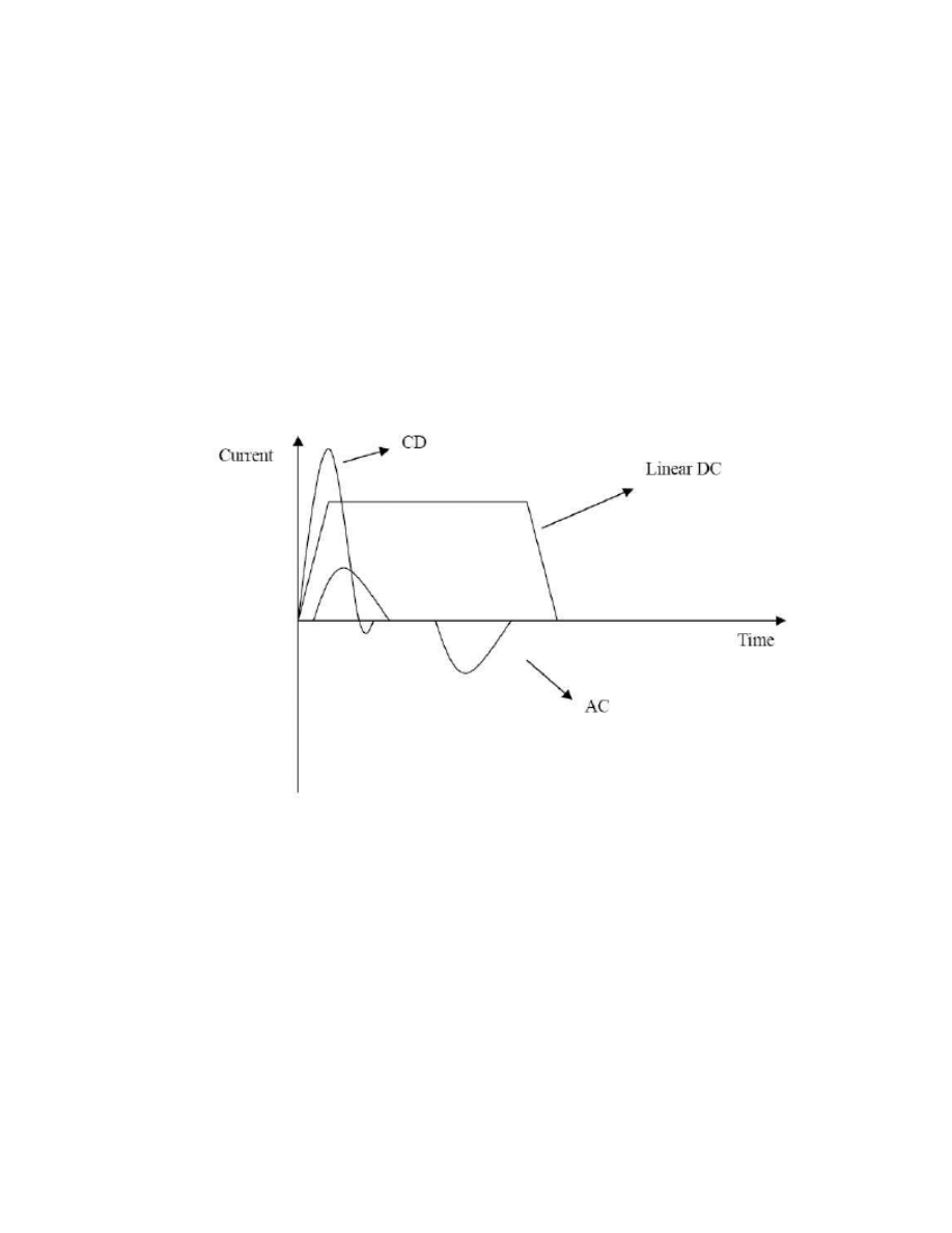
discharging the energy stored in a capacitor bank. Typical AC, CD and DC current
waveforms are shown in Figure
2-5.
Most large-scale resistance spot-welding systems use line frequency AC power
supplies [5]. When an AC power supply is used, output current is generally a sinusoidal
waveform of the same frequency as the input power line current, which is 50/60Hz
alternating current AC, and the heat is controlled by changing voltage and switching off
the current for a portion of each cycle. Through the use of silicon-controlled rectifiers
(SCR), the current is conducted in a controlled manner; therefore the resultant current to
the workpieces appears as shown in Figure
2-5.
The original AC power supplies were open loop controls. In order to improve the
welding quality and consistency, new AC welding technology that provides closed loop
control over weld current has appeared, but it has poor control ability at short cycle times.
This type of power supply is normally sensitive to the power line voltage change, which
is another limitation of the AC power supply. The advantages of the AC power supply
are: reliable, rugged and inexpensive.
A newer technology finding wide application in industry is the mid-frequency DC
supply. With this approach, standard 50/60Hz AC power is first rectified, converted to a

18
400 to 2000Hz AC with an inverter, stepped down through a transformer and then
rectified again. The final stage of rectification is necessary since at these higher
frequencies, the cable impedance will be more than an order of magnitude greater than
the weld resistance. Control of the amount of power supplied is achieved at the inverter
stage. The mid frequency DC (MFDC) power transformer has the identical purpose as
with the weld transformer in the traditional AC welder. The major difference lies in the
size of the magnetic iron core that transform primary current into secondary current.
Since the MFDC transformer operates with frequencies of 400 to 2000Hz instead of the
base 50/60Hz, the amount of iron in the core is reduced significantly. This allows the
transformer to be placed much closer to the welding tool in some cases hence providing
further benefits. It appears that the MFDC does not cause line disturbances, as the case
with the traditional AC welder. In fact, there are advantages for the electrical power
supply to install MFDC transformers for resistance welding [24]. It is a preferred
technology for higher currents associated with welding aluminum. Even with the smaller
transformer, the price of the power supply however is significantly more expensive than
traditional power supplies.
Downsized welder power supplies are used for small-scale RSW systems
(SSRSW). Most SSRSW applications use ”closed loop” controlled power supplies
including constant current, voltage and power control modes and providing faster speed
and smaller time intervals, such as linear DC power supply. A linear DC power supply is
also called a “transistor direct power supply”. A linear DC power supply consists of a
transformer, an ac-dc rectifier, a capacitor bank and power transistors. The transformer
steps down the high voltage from power lines to a lower level welding voltage. Then
through the rectifier, the ac current is converted to dc current, and the capacitor bank is
used to filter the signal and minimize the ripple. Finally, the controlled transistors act as
a direct current source to deliver the pure DC current to the weld tips and the workpieces.
This technology has excellent control repeatability, but the restriction to low power
restricts it to thin foils and fine wires and very low duty cycles [4], [8].
Some SSRSW applications use CD power supplies, which use “open loop”
control. It is also called a “Stored Energy” power supply
[22]. When a CD power supply
19
is used, a charged capacitor bank provides the energy and the amount delivered is
determined by the initial charge, i.e., initial voltage across capacitance. This kind of
energy source exhibits good repeatability of the amount of stored energy, and it is rugged
and inexpensive. However since the shape of the pulse is affected by the weld resistance,
the instantaneous weld powers are uncontrolled. Variability of weld conductor
impedance changes the energy delivered to the weld. Variability of the weld resistance
significantly impacts duration of weld and amount of heat dissipated during weld,
resulting in variability of final temperature and weld properties. Furthermore, due to the
limits on the capacitor size, it limits this approach to only SSRSW.
Figure
2-5: Sketch of current waveforms of CD, DC and AC power supplies
A switch mode DC power supply was used in our research. This power supply
was used as it provided no restrictions on controller implementations or strategy.
Commercial power supplies generally are restricted to applying fixed current or voltage
set points and are not easily modifiable. The present power supply is a small-scale spot
welding supply but can easily be upgraded to a full-scale spot welder. The power supply
is a pulse width modulated DC-DC converter. Thus its nominal output is given by the
duty cycle times the maximum voltage.

20
2.2.3
Resistance Spot Welding Sequence
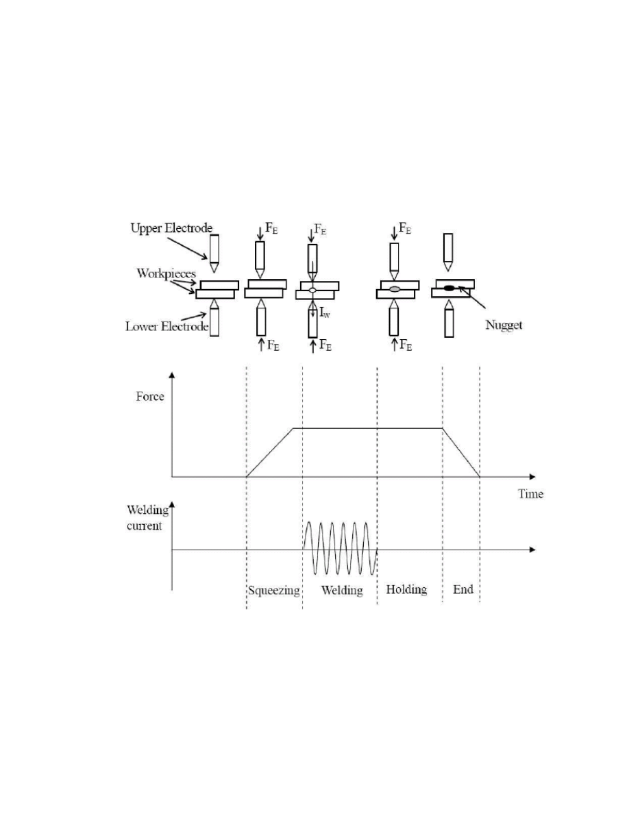
The spot-welding process is composed of a series of discrete events that occur over a
short period of time as shown in Figure
2-6
[25]. During “squeezing”, the electrode
move together; the force is applied from a pneumatic cylinder and reaches its preset
steady state value. The weld force will make the two workpieces contact well and then
provide proper faying resistance for the heat generation. The second step of the RSW is
called “welding”, when the welding current is conveyed by the electrodes to the
workpieces; it generates the energy to melt the contacted parts of the workpieces to form
the nugget. Real time closed-loop control is applied during this step, which is provided
by the welding power supply. The last step of a RSW welding is “hold”, which is also
called “cooling time”. The purpose of this step is to hold the molten nugget of the
workpieces for a certain period of time until it cools down and becomes a stable and solid
nugget. The welding force is still employed in this step to hold the joints. To finish, the
upper electrode is lifted up allowing the workpieces to be moved away and gets ready to
start the next weld.
It has been indicated that nugget formation and development can be characterized
as a function of welding variables (weld time, current and electrode force) by following
the principle stages
[26]:
• Initiation of nugget,
• Rapid nugget growth,
• Steadily decreasing growth,
• Possible weld metal expulsion.
As the contact resistance is strongly influenced by the pressure, electrode force is
believed to be a critical factor affecting the process, especially at the early stages in the
heating cycle
[27]. Higher electrode force usually reduces the contact resistance at the
electrode-sheet interface and, hence, would decrease the heat/temperature at the surface,
which may reduce the tendency of expulsion. Therefore, electrode force determines the
21
maximum nugget diameter without expulsion when the electrode geometry is kept
constant. By delaying expulsion, increasing electrode force can broaden the process
window for successful welding. However, a large force reduces the weld resistance
requiring higher current levels increasing the cost of the process. Further, a large
electrode force leads to damage of the electrode and can lead to excessive surface
indentation, which is often undesirable during micro-joining or precision welding.
Figure
2-6: The procedure of RSW
Welding current is another significant variable affecting nugget formation and
growth as the power generated is proportional to the square of welding current as
indicated in equation (2.1). The current range is determined by evaluating the minimum

22
and maximum current levels permissible for required joint properties
[28]. A certain
level of welding current is generally required to produce adequate heat energy for a weld
with a minimum nugget diameter. However, excess welding current causes void and
crack formations.
The effect of welding time can be also observed during the formation of weld
nugget. A longer weld time allows more heat to be conducted to the sheet metal.
However, longer weld time would increase the softening effect at the heat-affected zone
and hence decrease the joint strength when welding cold-worked sheet metal (such as Al
sheet)
[29].
The weld time, weld current and weld force are the key control variables for
regulating the quality of the weld nugget. These variables are strongly cross-coupled and
thus any of these parameters may be adjusted to influence the quality of the spot weld
produced, within a moderate range of values. The resulting weld may exhibit a few
characteristics that often serve as indicators of the weld quality
[30].
• Expulsion: Expulsion is the most frequently noticed indicator of weld quality.
This is a characteristic of over-welding where molten metal is expelled from the
weld nugget as a violent shower of sparks. The latest theory of expulsion is that it
happens when the force from the nugget due to the internal pressure in a liquid
nugget caused by melting, liquid expansion, and other factors exceeds the force
from the electrodes
[31]. Severe expulsion can reduce the joint strength because
of the loss of metal volume. In addition, expulsion has a negative influence on
adhesive bonding, if it is used in conjunction with spot welding, by damaging the
adhesive layer; therefore, it should be avoided. According to this theory expulsion
always occurs towards the end of the weld time as a nugget must have
overdeveloped in order for this condition to have occurred.
• Surface expulsion: This is produced when worn or misaligned electrodes are used.
Degradation of the tip of the electrodes increases the resistance of the interface
between the electrode and the workpiece. An increase in this resistance results in
a higher proportion of the welding energy being dissipated into this interface
23
causing localized melting to occur at the interface of the workpiece. This molten
material may then be released via a similar mechanism to normal expulsion;
however, this condition is generally less violent. The high electrode temperatures
generated by this condition promote further erosion of the electrodes thus
adversely affecting electrode life.
• Cold weld: This is a result of severe under-welding where a weld nugget does not
form. Insufficient current or a short weld duration causing insufficient energy to
be put into the weld zone causes this.
• Under-size weld: This is a spot weld where a nugget has formed; however, the
nugget diameter is less than the minimum size specified in the design. The
required nugget diameter is dependent on the classification of the spot weld. Both
expulsion and undersize welds are often used as visual indicators of a correct
welding process.
• Sparking: This occurs at the electrode-workpiece interface when the weld current
is initiated before electrode set-down. The sparks are generated when the
electrodes contact the workpieces resulting in erosion on the electrode surface and
may result in the electrodes becoming bonded to the workpiece. Severe sparking
can inflict significant damage to electrodes in a single weld.
Figure
2-7: Schematic of a typical RSW monitoring and control system

24
2.2.4
Signals Commonly Monitored during Welding Process
Monitoring a welding process provides useful information on the physical processes
involved in welding, and is a necessary step toward successful control of the process.
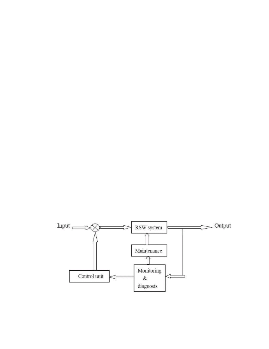
A general-purpose RSW monitoring and control system consists of three parts (as
shown in Figure
2-7)
[32]: a welding system, a monitoring unit and a control unit. The
system begins with an input to the welder, usually in the form of a welding schedule
specifying welding current or voltage depending on the weld controller, time, and
electrode force. The output of the welder is then fed into the monitoring unit, which
comprises data acquisition and signal processing. The processed information is then
passed on to the control unit. If an action is warranted, the control unit will modify the
input and alter the schedules for the subsequent welding process. In this section,
common signals collected during RSW are discussed, and their use for welding process
monitoring is presented. Intuitively, welding voltage and current should be monitored, as
they are directly related to joule heating, or the formation of a weld nugget.
Electric Current: Welding current is an important variable to monitor. This variable is
considered as the objective of advanced commercial control systems to keep the heat
generation consistent. It is usually measured using either a sensor based on the hall-effect
or a toroid sensor. The welding current itself does not represent the input heat. In order
to determine the heat input to a weld, both voltage and current must be measured.
Electrode Tip Voltage: Monitoring the electrode tip voltage can provide very valuable
information about the weld process. Although the voltage itself does not directly
represent the heat generation or nugget growth, a number of adaptive control units have
been developed that shut off the current at some predetermined voltage level
[33],
[34].
However, the tip voltage cannot be measured directly in an AC RSW circuit. So it
is not common to monitor this signal. Since the voltage probes must span the thickness
of the workpieces, a loop will exist in the voltage measuring circuit, and an inductive
voltage proportional to the derivative of the secondary current will be introduced
[25]. It
is well known that to minimize the inductive noise, one can use twisted pairs to reduce

25
the area of the wire loop. However, because of the large currents involved, the
constraints on placing the measuring wires to allow access to the workpieces, the induced
voltages are inevitably larger than the actual tip voltage
[35]. Thus, in practice with AC
welding supplies, voltage is measured only once per half cycle at the peak current when
the induced voltage is zero. For mid-frequency and switch mode DC supplies, the
bandwidth of current sensing must be kept well below the switching speed of the DC
supply.
Dynamic Resistance: Dynamic resistance is a measure of the electrical resistance change
during welding. Resistance is found by dividing the measured voltage by the current.
Hence all of the same difficulties for measuring tip voltage apply to finding the
resistance. Further for AC welding, no resistance can be determined for those periods
where the weld current is zero or close to zero. Dynamic resistance has been shown to
have a good correlation to the nugget growth and is currently receiving more attention
[60].
The phenomena occurring during spot weld formation can be understood through
analysis of dynamic resistance curves. Figure
2-4 shows the typical dynamic resistance
for the resistance spot welding process. After an initial drop, it rises to a peak in the first
portion of the weld cycle, dropping off later in the cycle. If expulsion occurred during a
spot weld, it is readily detected from a continuous measurement of this parameter. Since
expulsion results in a loss of metal, after expulsion the electrodes will move closer
together resulting in a shorter current path and a lower resistance. The main indicator for
expulsion is the instantaneous drop in the resistance.
Electrode Displacement: Electrode displacement is generally regarded as one of the
variables that can provide real-time information useful for monitoring and controlling
RSW process quality
[36],
[37]. It gives good indication of thermal expansion, melting,
and expulsion, and it has proven to be a particularly useful signal to monitor the welding
quality. However, in SSRSW production, it is difficult to measure the displacement
because its magnitude is very small, therefore different sensors such as fiber optic

26
sensors, etc. need to be used to monitor this variable to help in controlling the RSW
process.
Acoustic Emission: Acoustic emission is an outlet parameter which provides some
information about the process of resistance spot welding, as well as about the quality of
the weld spot. The information gained from acoustic emission can strongly support or
reject conclusions about weld quality by simply monitoring a single physical property.
Acoustic emission is the phenomenon of transient elastic wave generation due to rapid
release of strain energy caused by a structural alteration in a solid material. These
structural alterations can be the result of either an internally or externally applied
mechanical or thermal stress.
There are a variety of sources of acoustic emission signals ranging from atomic
scale to macrostructural changes in material. Typical sources of acoustic emission
include movement of dislocations along grain boundaries, microcracks and cracks, and
phase transformations
[28]
[38].
During the welding process two types of acoustic emission signals appear: useful
signals and disturbances. The useful signals contain information about events, which
take place due to the essential changes in the melted region of the spot weld and in the
heat affected zone. These signals are generated in both characteristic phases: during the
creation of the spot weld (while the welding current is running), and in the cooling phase.
The disturbance signals are various noises, which are not directly connected with changes
in the weld formation; they are caused by noise from the surroundings, noise in the
electrical network, noise of the cooling liquid, and knocks of the electrodes. The acoustic
emission sensor can be placed in two ways during resistance spot welding process; sensor
on the welding piece or sensor on the electrode. Choosing one of the two methods
depends on the purpose of the research and also on which of the phenomena in the
welding process is of the most concern.
For assuring quality welds, the electrical current, tip voltage, dynamic resistance,
electrode displacement, and acoustic emission signals have been the most used in
monitoring and controlling the welding process.

27
2.3
Small Scale RSW and Micro-RSW
Large-scale resistance spot welding is well over 100 years old and represents a mature
joining process
[39]. There has been ample time for materials to become standardized as
to alloy types, plating, and thickness. These factors have driven the creation of welding
tables that clearly define the large-scale resistance spot welding process for many
standard materials. However, when new alloys, such as advanced high strength steels,
and dual phase steels are developed and introduced, new tables are required before
industry will incorporate these materials.
In recent years there is an increasing need for very thin metal welding
applications. Extensive research and development work has penetrated in the area of
small and micro-scale resistance spot welding. Small and micro-scale resistance spot
welding is being fuelled by the explosion to make everything smaller, from automotive
electronics, to telecommunications components and medical products.
The monitoring and control of the small and micro scale resistance spot welding
process is less commonly addressed in the literature than the LSRSW process although
there are some significant differences between the two
[40]. Since the workpiece in the
small and micro scale process is relatively thin, electrode displacement monitoring
requires higher resolution and is much more difficult than for the large-scale process.
The small and micro scale process is relatively fast, the welding time being typically tens
of milliseconds instead of hundreds of milliseconds. The much smaller currents permit
the use of higher bandwidth high frequency inverter or linear power supplies rather than
low-to-medium frequency inverter used in the large-scale process. Also the small and
micro scale process uses much smaller electrodes and thus to achieve the same pressure
smaller forces.
According to the thickness of the joint metal sheet the RSW can be classified into
three classes, large scale RSW (LSRSW), small scale RSW (SSRSW) and micro-RSW.
LSRSW usually deals with metal sheets with a thickness above 0.41 to 1.57mm, while
Micro-RSW handles workpieces thinner than 0.125mm, and SSRSW works on the

28
workpieces with a thickness between the other two classes. Table
2-2 presents a
comparison of the three RSW classes
[12].
Table
2-2: Comparison between LSRS, SSRSW and Micro-RSW
G r o u p s
T h i c k n e s s
Ty p i c a l
C o m m o n A p p l i c a t i o n s
C o l d R o l l
A u t o b o d y, A p p l i a n c e s
L S R S W
0 . 4 1 – 1 . 5 7
S t a i n l e s s
S t e e l F u r n i t u r e
B r a s s A l l o y s
E l e c t r o n i c Te r m i n a l s
C o p p e r
E l e c t r o n i c Te r m i n a l s
C o p p e r A l l o y s
B i - M e t a l C o m p o n e n t s
I n c o n e l
A i r c r a f t C o m p o n e n t s
M o l y b d e n u m
A u t o H e a d l a m p s
N i c h r o m e
B i - M e t a l S e n s o r s
S i l v e r A l l o y s
R e l a y C o n t a c t s
S t a i n l e s s
S m a l l S u r g i c a l I n s t r u m e n t s
S S R S W
0 . 1 2 5 – 0 . 5 1
T u n g s t e n
A u t o H e a d l a m p s
C o p p e r
Electronic Circuit Connections
G o l d
Electronic Circuit Connections
N i c k e l
Electronic Circuit Connections
N i t i n o l
M e d i c a l G u i d e Wi r e s , S t e n t s
P l a t i n u m
Electronic Circuit Connections
M i c r o -
R S W
0 . 0 1 2 5 –
0 . 1 2 5
S t a i n l e s s
M i c r o - C u t t i n g I n s t r u m e n t s

29
Chapter 3
3
Weld Power Supply
Industrial weldering power supplies are expensive to install and not flexible for RSW
monitoring and control research. Therefore, in order to perform RSW monitoring and
control research at University of Western Ontario (UWO) to improve the consistency of
RSW, a DC power supply for micro welding machine was designed and developed in
2005 by Dr. L. J. Brown and J. Lin, and it was awarded a patent in 2004
[6],
[7],
[8].
3.1 Previous Power Supply Design for SSRSW
All the presented information in this section regarding the design of the previous power
supply for SSRSW is based on a paper presented at the AWS Welding Show and Annual
Convention held on April 25-28, 2005, in Dallas, Tex, as well as the master’s thesis for J.
Lin [42, 43, 44]. This power supply uses pulse width modulation technique, with low
cost MOSFETs, to convert the power of a 12-V battery to a weld current up to 1000A.
Microprocessor/controller technology, which provides the flexibility for the application
of different control schemes, such as constant voltage control, constant current control
and constant power control, was used in this power supply design
[6],
[7],
[8],
[42], and
[43]. Figure
3-1 shows the system diagram of a SSRSW system, which consists of a
micro welding machine, a DC power supply, a 12-V battery, and a battery charger.
Figure
3-1: SSRSW system
[42]
This power supply consists of three major sections: power section, control
electronics section, and the microcontroller. Figure
3-2 illustrates the system block
diagram.
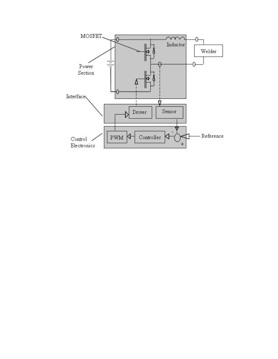
30
Figure
3-2: System block diagram
[42]
The power section converts the input power from the 12-V battery to an
appropriate output voltage to feed the welding machine. Power MOSFETs switch at a
frequency of 20 kHZ, and are used as the switching components. The output current is
filtered using an output inductor as a filter. The control electronics section includes the
driver circuits for the MOSFETs, and the sensing circuits for voltage and current.
The choice of an inductor to filter out the ripple instead of a traditional capacitor
is due to the fact that the load resistance is in the 1-10mΩ range. Thus for a worst case
filtering time constant of 1ms, the design would need an inductor of 10µH versus a
capacitance of 1F. This type of filtering makes it more natural to view the power supply
as a current source rather than as a voltage source. The control electronics section
includes the driver circuits for the MOSFETs, and the sensing circuits for voltage and
current.
The microcontroller includes both the hardware and software, which is the central
control unit of the system. The microcontroller implements the control schemes and
provides the PWM signal to drive the MOSFETs in the power section, which is based on
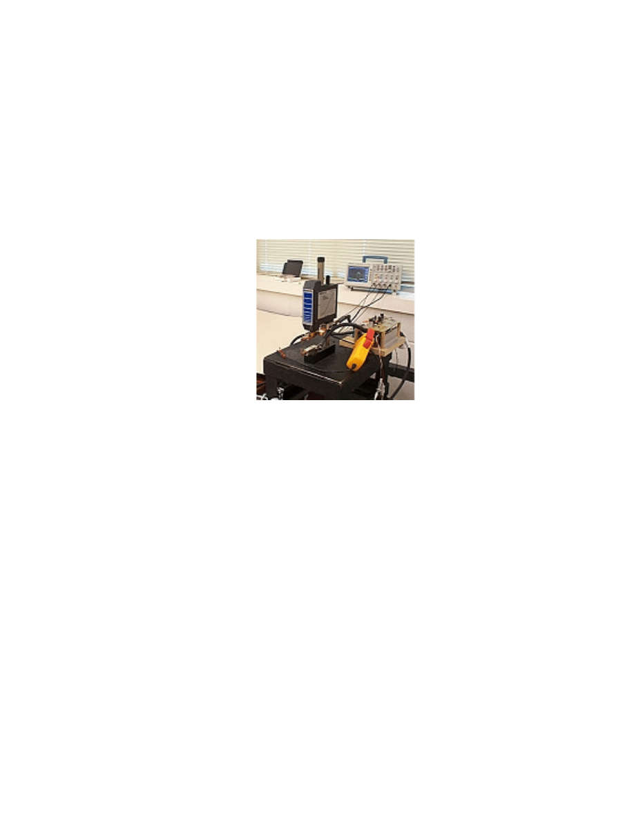
31
the given reference and feedback signals. An 8-bit microcontroller, PIC16F73 from
Microchip, Inc., was selected as the CPU of the system
[6],
[7],
[8],
[42], and
[43]. Due
to the computation limitations of this processor, the controller was restricted to the
form
1
sign( )
k
k
k
D
D
K
e
−
=
+
, where D
k
is the duty cycle and e
k
was the difference between the
control variables actual and desired value and K is the constant value used to update the
duty cycle. The control variable was restricted to duty cycle, current or power. Figure
3-3 shows the actual design for the previous DC power supply.
Figure
3-3: Actual experimental setup
[42]
3.1.1
Power Section
This section will explain the design and operation for the power section that was
previously designed for the novel DC power supply for SSRSW, which is also used in the
modified DC power supply unit presented in this thesis with no changes to its original
design.
A DC power converter has been designed for SSRSW applications. Figure
3-4
shows the configuration of the power section, which contains the following four
components:
• A half bridge of power MOSFETs, Q1 & Q2
• A capacitor bank, C
• An inductor, L
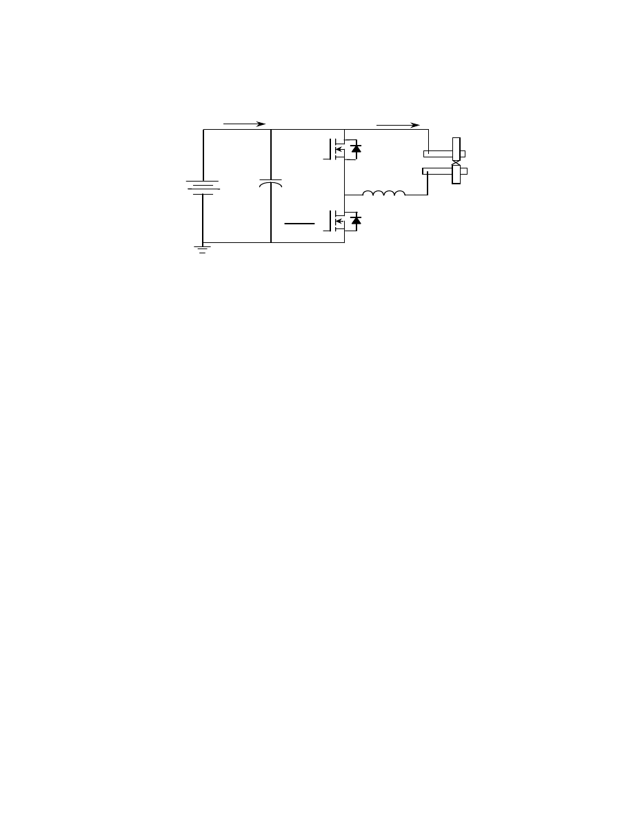
32
• A car-battery, Vs
Q 2
Q 1
L
W eld er
C
1 2 V
B attery
Iin
Io ut
P W M
P W M
Figure
3-4: Power section
[42]
The half bridge (MOSFETs (Q1 & Q2)) works as a buck converter with the
capability of freewheeling the load current through MOSFET Q1. For high current rating
design, the schematic transistors are composed of 2 transistors in parallel. The low-side
MOSFET Q2 is the main power switch, which regulates the output power. The high-side
MOSFET Q1 works as a freewheeling switch, which provides a current path for the load
current when Q2 is off. The idea of using MOSFETs instead of diodes for freewheeling
has two advantages: less loses due to the less voltage drop across MOSFET than diode,
and the good load current sharing feature of MOSFETs. MOSFETs have a positive
thermal feature, i.e., the higher the junction temperature, the higher the on-state resistor.
Therefore if one MOSFET is more loaded than others, its junction temperature becomes
higher, so does its on-state resistance, and then it takes less load current, letting the other
MOSFETs take a greater share. This way all the MOSFETs together share the load
current in balance.
On the other hand, if two or more diodes are put in parallel, since the forward
voltage drop differs in each individual diode, the greater current will flow through the
diode with the lowest voltage drop, which will increase the heating and lower the voltage
drop further. This will damage the diode with the lowest voltage drop, and then the
current will move to the next one. Therefore it is a less desirable design to use diode in
parallel to share the current.

33
The capacitor bank C assists in providing the ripple current required by the high
frequency switching. The inductor L works as a current choke, which filters out the
ripple on the load current caused by the high frequency switching. The selection of the
inductance L is discussed below at the end of the steady state analysis of the operation.
The car battery Vs is the energy source of the power supply.
High frequency switching technology is used in the design. The selection of the
switching frequency is usually a trade-off of the switching loss, the component sizes and
the acoustic noise. A lower frequency is desired for lower switching loss, since the
switching loss is proportional to the switching frequency. On the other hand, the lower
the switching frequency, the higher the inductance will be required in the circuit and the
slower the response of the circuit. Therefore a higher switching frequency should be
selected to reduce the sizes of the capacitor C and the inductor L. In this thesis, a
switching frequency of 20 kHz is used, which is just above the acoustic noise range. The
MOSFETs are controlled by pulse width modulation (PWM) signals generated though
either the PWM analog circuit or the DSP board. The output power is regulated through
the control of the duty ratio D of the PWM signals. The detail of the control schemes is
discussed in later sections in this thesis.
Steady State Analysis
To simplify the analysis, the following assumptions have been made:
• The circuit is operating at steady state, the duty ratio D and load current have already
stabilized;
• The MOSFETs Q1 and Q2 are ideal switching components;
• The load (welder) is considered as a constant resistor; although the resistance changes
along with the welding process, the time constant of this change is much bigger than
the switching period (50µs), therefore it is reasonable to consider the resistance as a
constant within the switching of the MOSFET.
• The load current (
L
I
) is continuous due to the sufficient inductance in the design.
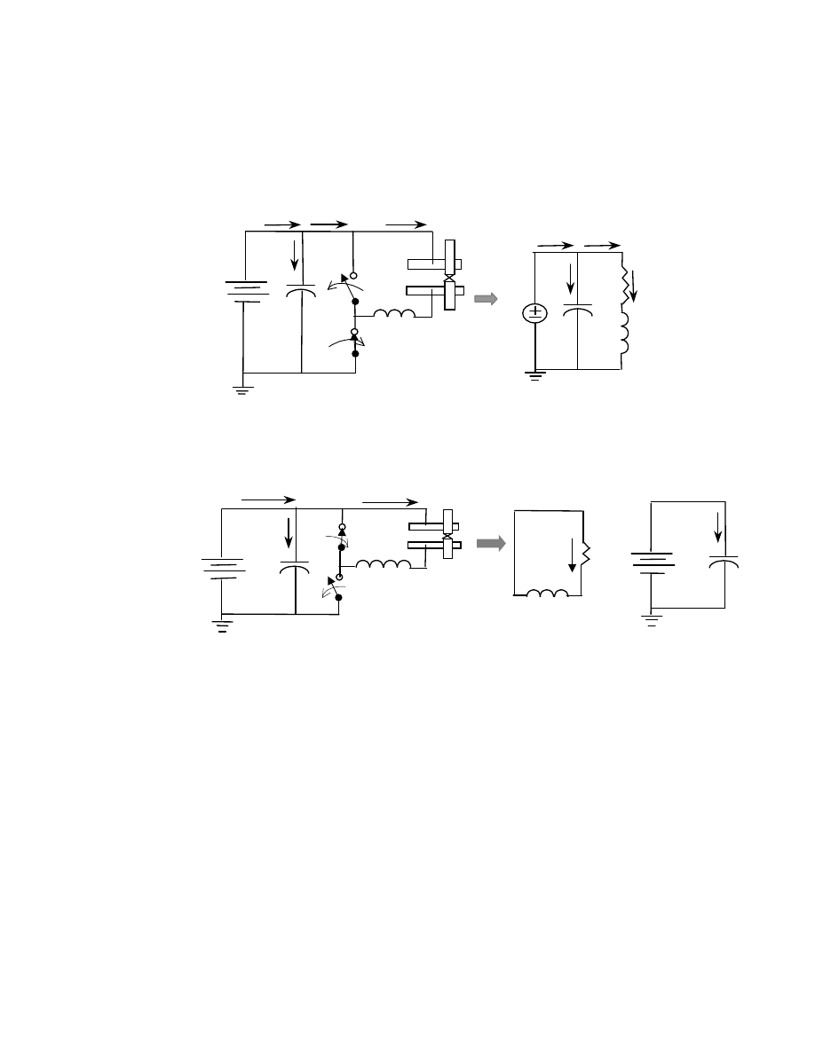
34
The power converter has two operating states: powering state with Q1 off, Q2 on,
and freewheeling state with Q1 on, Q2 off. The following figure shows the equivalent
circuits for these two states.
L
Welder
C
12V
Battery
I
i
I
L
I
m
I
c
I
i
I
m
I
c
I
L
V
o
Vs
Q1
Q2
R
L
(a)
Powering, Q1 off, Q2 on
L
Welder
12V
Battery
I
L
I
i
I
L
C
I
c
Q2
R
Q1
L
C
I
c
(b) Freewheeling, Q1 on, Q2 off
Figure
3-5: Steady state equivalent circuits
[42]
3.1.1.1
Analysis of Powering State, Q1 off, Q2 on
When Q2 is turned on, Q1 will be turned off to avoid the failure of shoot through. The
voltages on Q1 and Q2 are:
1
2
0
Q
s
Q
V
V
V
=
=
(3.1)
The battery provides the input current (
i
I
) to the system through the capacitor bank,
which provides the ripple current required by the high frequency switching. The input

35
current (
i
I
) can be considered as unchanged within the switching period. The middle-
stage current (
m
I
) equals to the load current (
L
I
), which is the same as the inductor
current, since they are in series. (Figure
3-5 (a)).
m
L
I
I
=
(3.2)
The relationship between the input current (
i
I
), the middle current (
m
I
) and the capacitor
current (
c
I
) is:
i
m
c
L
c
I
I
I
I
I
=
+
=
+
(3.3)
The source voltage (
s
V
) is applied to the load (welder) and the inductor. Therefore the
load current increases.
(
)
1
0
L
s
L
L
s
L
dI
V
R I
L
dt
dI
V
R I
dt
L
=
⋅
+
=
− ⋅
>
(3.4)
The voltage applied on the welder tips is
o
L
V
R I
=
⋅
. Figure
3-6 illustrates the waveforms
of these variables during the switching.
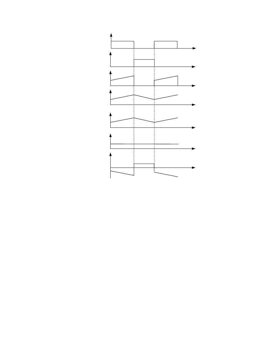
36
V
Q1
V
Q2
I
m
I
L
I
c
I
i
Q1 off
Q2 on
Q1 on
Q2 off
V
o
Figure
3-6: Steady state waveforms
[42]
3.1.1.2
Analysis of Freewheeling, Q1 on, Q2 off
When Q2 is turned off, Q1 will be turned on to provide a freewheeling path for the
inductive load current (
L
I
). The voltages on Q1 and Q2 are:
1
2
0
Q
Q
s
V
V
V
=
=
(3.5)
The middle-stage current (
m
I
) is zero since the load current (
L
I
) loops back through Q1,
and no energy is drawn from the power source. The capacitor takes all the input current
(
i
I
) to charge up (Figure
3-5 (b)).

37
0
m
c
i
I
I
I
=
=
(3.6)
The inductor discharges the stored energy to keep the current flowing, and the load
current (
L
I
) decreases.
0
0
L
L
L
L
dI
R I
L
dt
dI
R
I
dt
L
=
⋅
+
= −
⋅
<
(3.7)
3.1.1.3
Selection of the Inductance L
The purpose of the inductor L is to reduce the load current ripple caused by the switching.
Therefore the specified ripple current allowed in the system determines the inductance L.
To simplify the analysis, it is assumed that the current changes linearly within the
switching. The Figure
3-7 shows such a current profile.
I
max
I
ave
I
min
DT
T
t
i
Figure
3-7: Load current profile within a switching period
[42]
The equation used to select inductance is
[45]:
(1
)
2
D R
L
f
−
⋅
≥
⋅
(3.8)
In this thesis, f = 20 kHz, the maximum load resistance is estimated as 0.02 ohms,
and the duty ratio D is a number between 0 to 1, here 0.5 is chosen as D, then the

38
inductance is determined as:
6
0.5 0.02
25 10
2 20000
L
H
−
⋅
≥
≥
⋅
⋅
(3.9)
3.2
SSRSW Power Supply Modification
The main and first part of my Ph.D. research work was to modify the previously designed
SSRSW power supply. The modification that was done for the power supply was in the
controller section by replacing the 8-bit microcontroller, PIC 16F73 from Microchip, Inc.
with the option of using an externally supplied pulse width modulated (PWM) signal, or
generating its own PWM signal from an analog PWM chip. The set point for the analog
PWM chip can be generated internally as a fixed value, from a built-in analog PID
controller or from an external analog signal. Normally we generate the external PWM
signal from a DSPACE control board (DSP) with a controller implemented with Open
Desk software. Open Desk software, is a real time software that works as the interface
between DSP and the PID controller designed in Simulink, where weld current and tip
voltage actual signals are fed as feedbacks to the PID controller, as well as PID controller
output duty cycle is used to generate the PWM signal to drive the SSRSW power supply.
In total there are 5 operating modes for the modified power supply unit:
1)
External PWM signal
2)
External analog reference for the PID controller
3)
External analog duty cycle (D)
4)
Internally generated duty cycle (D)
5)
Internally generated reference with PID controller
Both the built-in controller and the controller implemented on the control board
have the option of using tip voltage or welding current as feedback variables. The full
use of these control variables for the control board will be discussed later in this thesis.
This configuration gives the flexibility to quickly test advanced, computationally

39
intensive control algorithms on the dedicated control board and then test the
implementation on extremely low cost commercially viable hardware. Moreover, the
combination of the inductor based output filtering and the ability to control the duty cycle
via externally generated analog value or PWM signal allows the units to be easily
connected in parallel. This allows research to be conducted at current levels (~10kA)
necessary for the standard gauges used for example in automotive industry welders.
3.3
SSRSW Power Supply System Requirements
The following Table gives a summary of the technical requirements for the SSRSW
power supply.
Table
3-1: Technical requirements
Welding current
50 ~ 1000 amps
Electrodes tip voltage
0.1 ~ 5 volt
Welding time length
15 ~ 99 milliseconds
Control modes
Open loop voltage, constant current, constant voltage and
generic power control
The individual parameter will be determined according to the specific welding
conditions, like material, thickness, force, etc. A Unitek Peco Model 80 Series Weld
Head has been chosen as the weld head. The welding force can be adjusted within a
range of 2 to 20lbs.
The setting of load current depends mainly on the material and dimension of the
workpieces, the geometry of electrodes, and the welding force. Typically, the DC
welding current should be of a range from hundreds of amps up to the maximum of
twenty five thousand amps. The material used in this research is 0.152mm stainless steel,
which requires a minimum current of around 250 amps. Electrode tip voltage is another
parameter for control of the welding qualities. The range of tip voltages for SSRSW can
be estimated based on the required welding current, typically from hundreds of millivolts
to several volts. The welding quality is affected by the setting of these parameters.

40
3.4
Electronic Circuits Designs for RSW Power Supply
Modified Unit
During the first part of my Ph.D. research work, three power supply units were built at
UWO lab for future use for LSRSW. The unit consists of 5 electronic circuits,
MOSFETs driver circuit, PID controller analog circuit, PWM circuit, timer circuit, and
sensors circuit. The design for each circuit will be explained in the following sections.
The full schematic design for each circuit is shown in the appendix.
3.4.1
Timer Circuit
The timer circuit is the driving circuit for the other 4 electronic circuits, see appendix for
the circuit schematic. The main three purposes for this circuit is to supply a normally
high (NH) signal for the PWM analog circuit to determine the switching period, as well
as supplying a normally low (NL) signal for the PID controller for the first 0.3ms, to
provide the weld enable signal and the pulse that controls the analog switches for the PID
controller circuit (see section 3.4.3). Finally, the third purpose is to supply another NL
signal to the MOSFETS driver circuit to enable the driver chip to start the weld.
It was designed using MC14538B chip from Motorola. This chip operates using
the basic 555 timer circuit
[54] operation. It has two 555 timer circuits built in, each
outputs two different output signals, one is NH and the other is NL, which is suitable for
our purpose in designing the power supply. The time for each timer circuit is precisely
controlled by one external resistor and capacitor. A 10K potentiometer with a 3.3µf
capacitor is connected to the first timer circuit to control the weld time. It is NH signal is
used by the PWM analog circuit to determine the switching period, while it is NL signal
is used by the MOSFETs driver circuit to enable the driver chip to start the weld for the
specified weld time. The second timer circuit is using a 100K resistor with a 3nf
capacitor, to provide the weld enable signal and the pulse that controls the analog
switches for the PID controller circuit for the first 0.3ms of the weld time. The following
time graph (Figure
3-8) shows the behavior of the three timer circuit outputs.
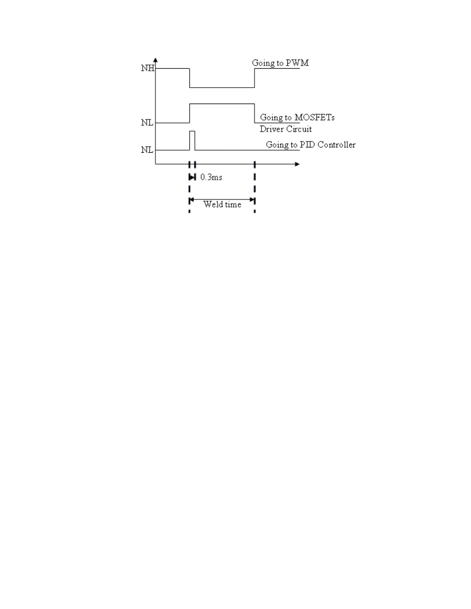
41
Figure
3-8: Timer circuit output signals graph
3.4.2
PWM Analog Circuit
The PWM analog circuit generates its signal based on the timer circuit as mentioned
above. Its output is used to drive the MOSFETs driver circuit. Two special input signals
are used to control the operation:
• PERIOD (T), determining the switching period
• DUTY, determining the duty ratio
The timer normally high (NH) signal is used for determining the on time for the
PWM analog circuit. For the purpose of this research, a PWM analog circuit with
SG3525A chip from Semiconductor was used. This chip has a shutdown pin, which is
connected to the NH output signal from the timer circuit, which activates the circuit once
the positive NH signal is applied. Once the NH signal goes low, the PWM chip outputs
its output signal to drive the MOSFETs driver circuit, and once it goes high again, the
shutdown pin immediately turns off the output signal for the PWM chip. Figure
3-9
illustrates the operation of the PWM signal with respect to the NH signal from the timer
circuit.
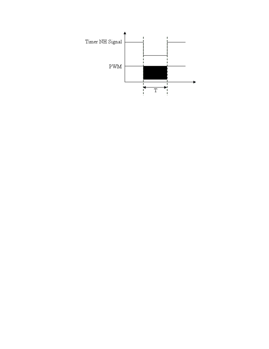
42
Figure
3-9: PWM & timer NH signal graph
For determining the duty ratio for the PWM analog circuit, another input signal is applied
to the non-inverting input of the PWM chip. This input signal can come from three
different control components, depending on the control mode that the power supply unit
will be running under. The three control components are:
• Manual control using a 10K potentiometer, that varies from 1V to 4V, with
approximately 1V being 0% duty cycle and 4V being 100% duty cycle. This input
signal is used under the open loop control mode.
• PID controller output signal, which is used under the closed loop control mode.
• DSP 5V logic output signal, which is used under the open loop/closed control mode
using DSP board.
3.4.3
PID Controller Analog Circuit
Three op-amps are used to design the PID controller analog circuit. The analog PID
circuit is shown in Figure
3-10. The feedback tip voltage and weld current signals come
from the sensors circuits (see section
3.4.5). The weld current sensor circuit outputs a
signal (V
sense
) from 2.5V to 0V; therefore the first op-amp is used to convert this signal to
go from 0V to 5V instead, by multiplying the signal by 2 and subtracting it from the V
sup
signal going into the negative input of the op-amp, which is approximately 5V. Equation
(3.10) represents the output voltage coming from the first op-amp and going into the
negative input of the second op-amp. The reason for that is to be able to use the output

43
voltage from the first op-amp with the second op-amp to be subtracted from the reference
signal, since the reference signal starts from 0V to 5V. While for the Tip Voltage signal,
the tip voltage sensor outputs a signal from 0 to 5V, therefore it is used directly by the
second op-amp, and the switch is used to switch between using the tip voltage signal or
the weld current signal as needed.
2
sup
sense
V
V
−
(3.10)
The second op-amp calculates the error signal, which is the difference between
the converted tip voltage signal or weld current signal and the desired reference signal,
which is used by the third op-amp that outputs the PID duty cycle. A 10K potentiometer
that varies from 0V to 5V is used to manually control the desired reference signal. The
following table show the components values connected to the first and second op-amps.
Table
3-2: First and second op-amps components values
Component
Value
R5
3.3kΩ
R6
4kΩ
R7
2kΩ
The third op-amp implements the PID controller three gains. By dividing the
feedback capacitor C1 by the input resistor R4, we get the integral gain for the controller.
Adding R3 in series with C1, and at frequencies above where the capacitance reactive of
C1 equals R3, we will have a gain of 1. That will give the proportional gain for the PID
controller. C2 is added in parallel with input resistor R4. At frequencies above where C2
equals R4, it will act as a differentiator, which will give the derivative gain for the PID
controller. The following equation (3.11) represents the transfer function for the PID
controller.

44
3
1
4
2
3
2
4
1
4
1
1
1
( )
1
P
I
D
R C
R C
F s
R C S
R C
R C
S
K
K
K S
S
+
= −
+
•
+
=
+
•
+
(3.11)
Therefore, the PID parameters are calculated as:
3
1
4
2
4
1
4
1
3
2
1
P
I
D
R C
R C
K
R C
K
R C
K
R C
+
=
=
=
(3.12)
Table
3-3 gives the values for the capacitors and resistors for the PID op-amp
circuit. These values were just chosen to test the PID circuit behaviour; more work in
choosing the right values for perfect tuning can be done for more future work. To ease
the process for future tuning for the PID controller, all its resistors and capacitors are
mounted on snap in socket. The selection of the PID gains is discussed in chapter 4.
Table
3-3: PID op-amp circuit components
Component
Value
R
3
13Ω
R
4
0.68Ω
C
1
0.01µF
C
2
0.001 µF
The welding process is a nonlinear process and thus the PID controller will be
tuned about its steady state operating point. Thus the analog controller must be designed
to transition from the off state to this steady state point before the PID controller is
invoked. Three analog switches were added to the PID analog circuit using CD4053BC
chip; to work together to ensure that the system will run open loop for a fixed time (Td),
before the PID gets engaged. When switches A, B & C are in the positions Ay, By, & Cy,
the capacitor C1 gets isolated from the PID circuit and charges to a fixed voltage (2.5V)

45
for a fixed time (Td), for the purpose of our research Td=0.3ms. Switch C disconnects
the PWM from receiving the PID duty cycle, and it receives a fixed duty cycle putting the
system initially in an open loop mode. After switches A, B, & C move to positions Ax,
Bx, & Cx, the capacitor C1 gets connected to the PID circuit, starting the integrator with
a controlled offset. Switch C connects the output of the PID controller to the input of the
PWM controller for the rest of the weld time, for the purpose of our research the weld
time is 20ms. The way R1, R2, D1 & D2 are connected is to limit the charging fixed
voltage for C1 when it is switched in, to 2.5V for the first 0.3ms of the weld time. R1 &
D1 are mainly to do the limiting process for charging C1 to 2.5V, while R2 & D2 are to
set the 2.5V for R1, D1, R2 & D2 circuit path. The analog timer circuit designed in
section 3.4.1 is used to provide the weld enable signal and the pulse that controls the
switches. Figure
3-11 shows the timing diagram for these signals. Table
3-4 give the
values for the components connected to the analog switch.
Table
3-4: Analog switch circuit components
Component
Value
R1=R2
10Ω
D1=D2
2.5V Zener Diode
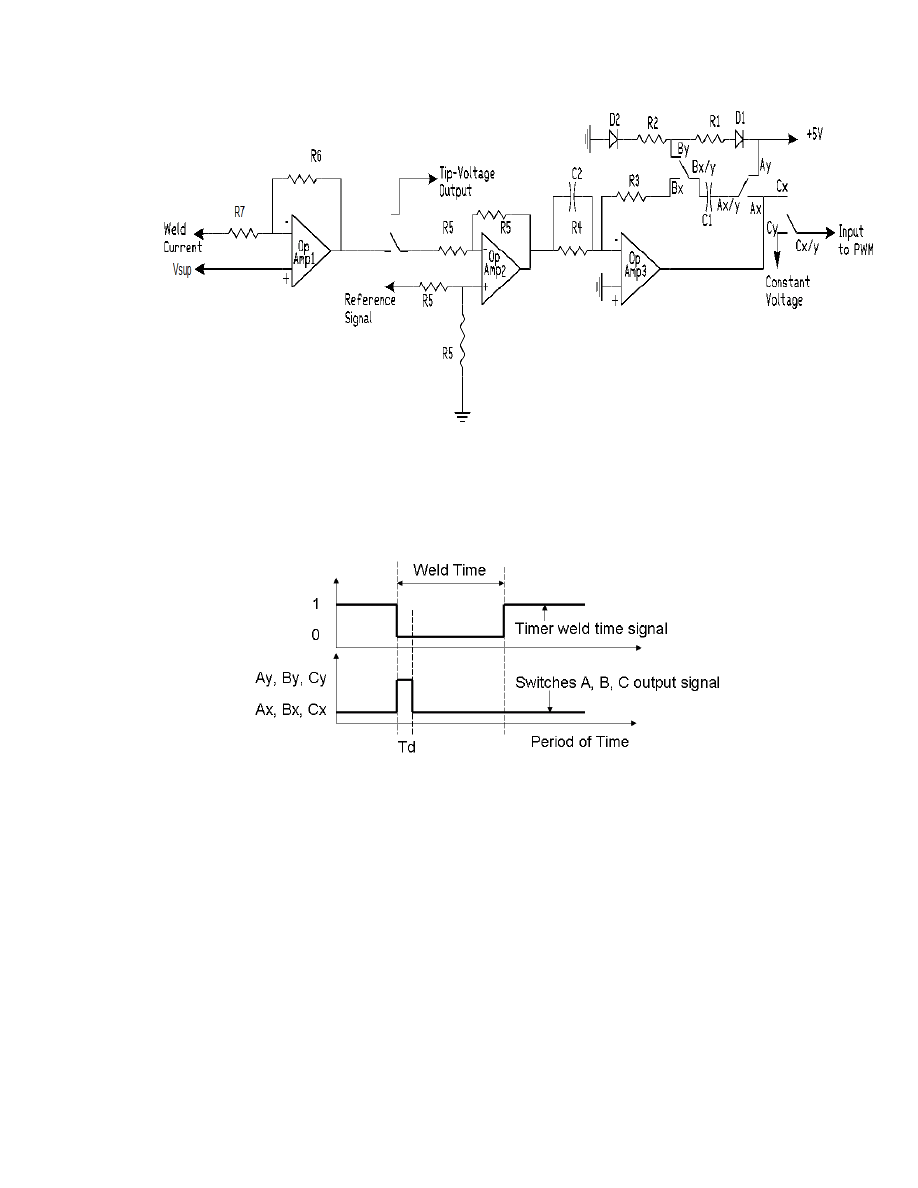
46
Figure
3-10: PID analog circuit
Figure
3-11: Analog switches timing graph
3.4.4
MOSFETs Driver Circuit
The driver circuit is designed to take the logic level (5V) PWM signal either from the
analog PWM circuit or from the DSP board, and outputs two gate signals G1 & G2 to
drive the high (Q1) and low (Q2) side MOSFETs. These gate signals have the following
features:
• Higher voltage level (23);
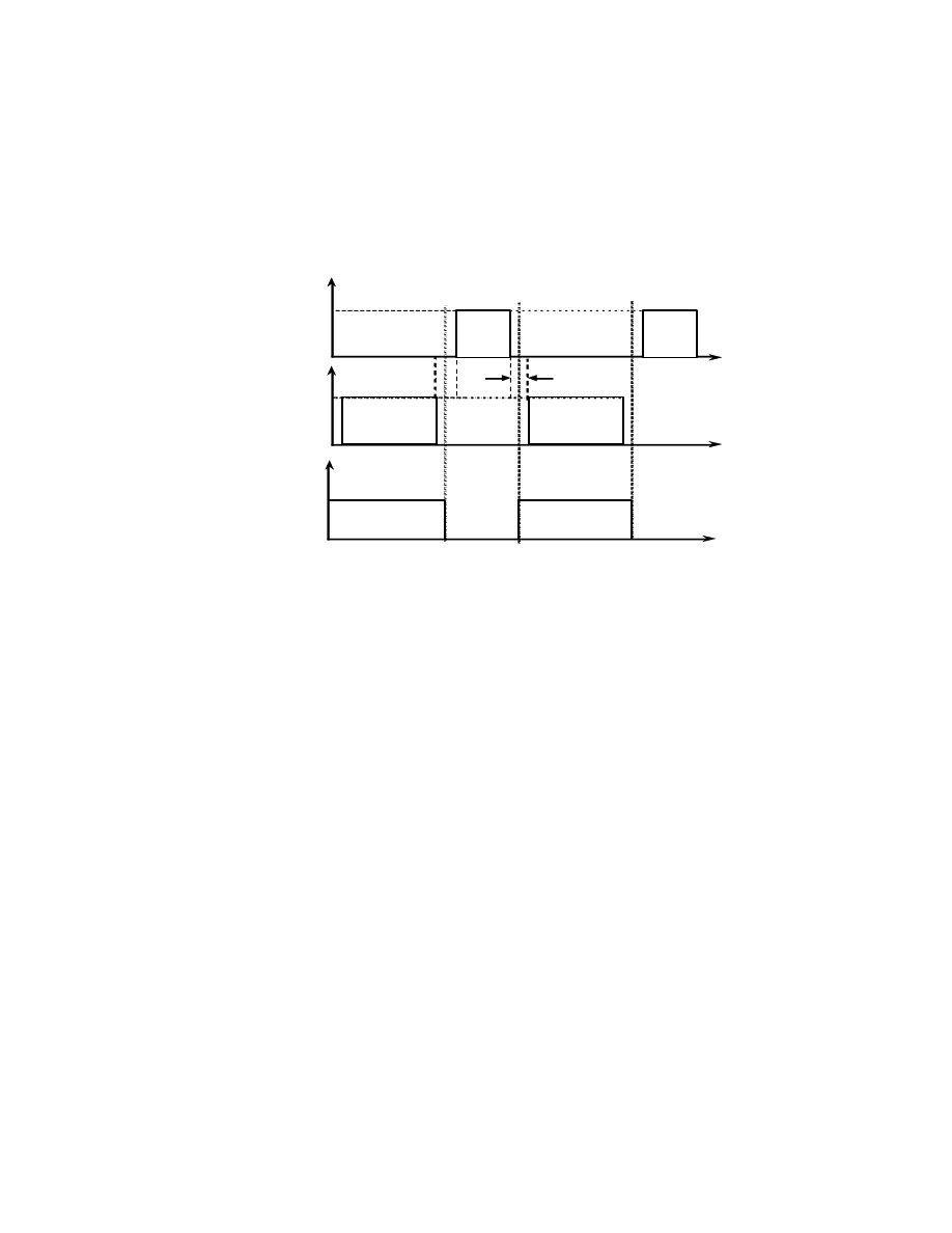
47
• Proper reference points of signal, G1 to the source of Q1, G2 to the source of Q2;
• Appropriate dead band between G1 & G2 to prevent shoot-through.
Figure
3-12 shows the relationship between the two gates G1, G2 and PWM signals.
G 1
t
t
P W M
5 V
2 3 V
G 2
t
1 2 V
D e a d b a n d
Figure
3-12: Driver gates G1, G2 & PWM signals
[42]
For the purpose of this research, an integrated driver circuit IR2184 from
International Rectifier (IR) has been used with a dead band of 500ns built in.
3.4.5
Sensing Circuits
The task of the sensing circuits is to transform the measured signals into proper voltage
signals that can be used by DSP board for monitoring and closed loop control purposes.
Three analog signals are used by the DSP board, force signal, tip voltage signal & weld
current signal. The force signal is used as a trigger by DSP board to start the weld time
after each time a spot weld is done. The control desk software for the DSP board, to reset
the timer for the specified weld time, uses the force signal. The force signal comes from
the welder head. Tip voltage and weld current signals are measured to support
implementing the control schemes using the software with the DSP board, as well as for
monitoring.
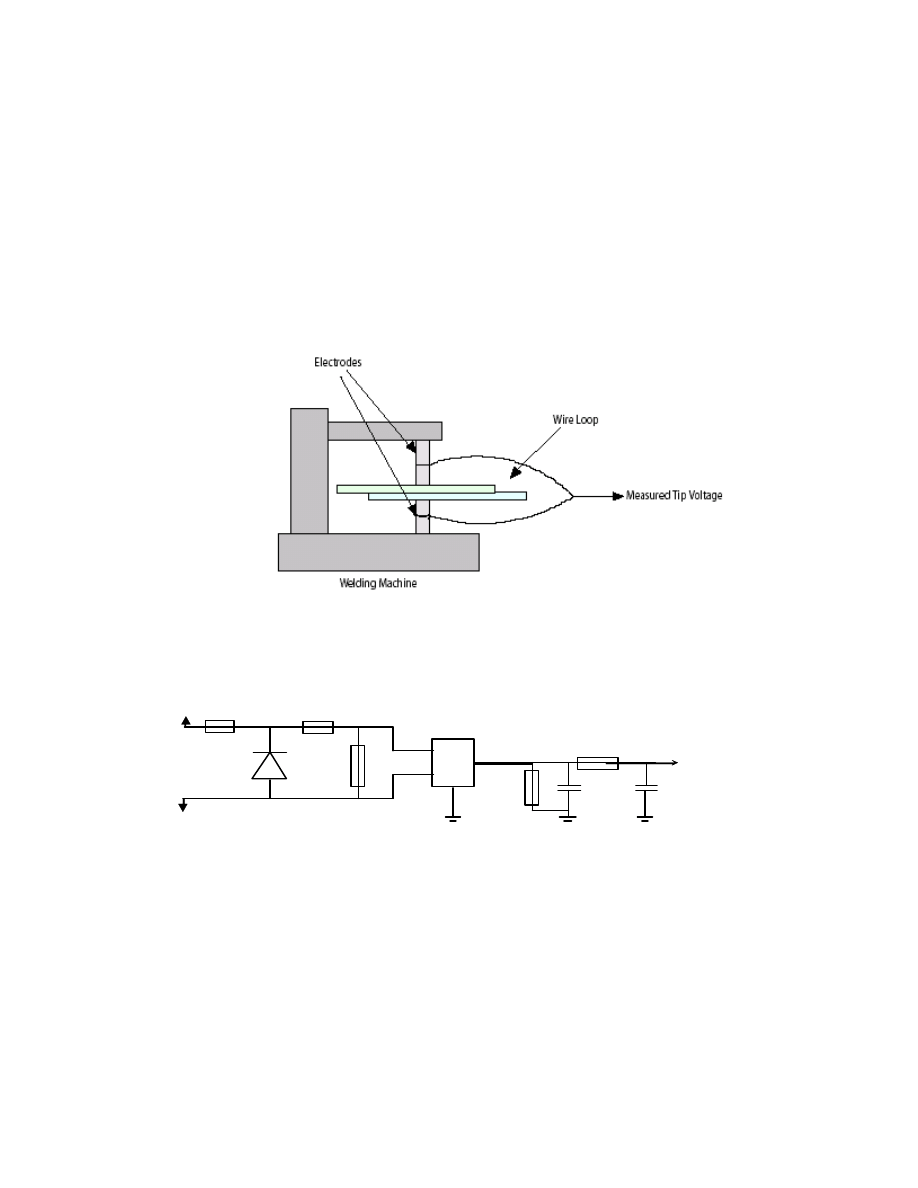
48
3.4.5.1
Tip Voltage Measurement
As shown in Figure
3-13, the sensing circuit for the tip voltage is designed using the
ZXCT1010 chip, which is a high side voltage monitor. The chip removes the large time
varying common mode voltage at the electrode tips and converts the measured signal to a
current signal. The circuit includes a low-pass filter at its output. The signal is available
for the DSP board, as well as the PID analog circuit. This chips outputs up to 2.5V sense
voltage.
(a)
Upper W elde r Tip
T o DS P /P ID
IC Chi p
(ZX CT1 010)
Low -pass
filt er
O utput
200Ω
0.1µ F
Low er W elde r Tip
100kΩ
50kΩ
3.3V
50kΩ
0.01µ F
12kΩ
(b)
Figure
3-13: Tip voltage (a) diagram
[42] & (b) circuit schematic
3.4.5.2
Weld Current Measurement
A hall-effect sensor and a magnetic core are used to measure the magnetic field induced
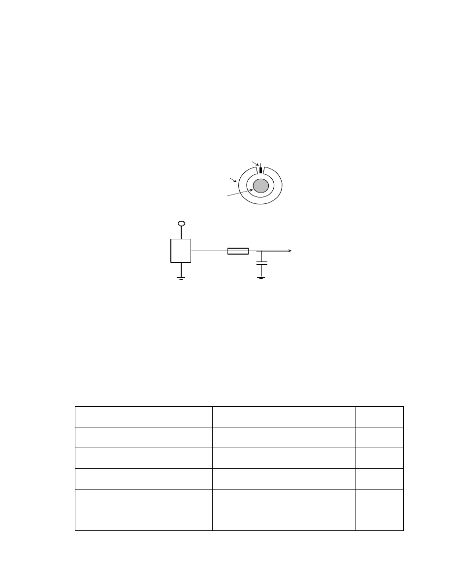
49
by the load current. The following figure shows the mechanical structure of the current
sensing circuit. The hall-effect sensor (Allegro 1302) transforms the magnetic field into a
proportional voltage signal with a resolution of 1.3 mV/Gauss. The voltage signal goes
through a low-pass filter, and is used by the DSP board, as well as the PID analog control
circuit. Figure
3-14 presents the circuit. Through experimental calibration, the scaling of
the current sensor is obtained as 4.659 A/mV.
H a ll-e ffe ct S enso r
X
M ag net ic co re
L o ad current
5V from D SP
To D S P/ PID
Hal l-effe ct
S ensor
(1 302)
L ow-pa ss
fil ter
O utput
12kΩ
0.01µF
Figure
3-14: Sensing circuit for weld current
[42],
[44]
3.4.6
Summary of the Main Components Used in the Modified
Power Supply Unit
Table
3-5 gives the summary of the components used in the SSRSW power supply
modified unit and Figure
3-15 shows the modified RSW power supply unit.
Table
3-5: Main components used in the modified power supply unit
Components
Specification
Quantities
Battery
12V lead acid battery
1
Inductor 1.7µH
6061 Alloy, 6 full turns on 3 levels
1
Capacitor bank
1800 µF
11
PID Op-Amps
• Single Op-Amp LM741
1
1
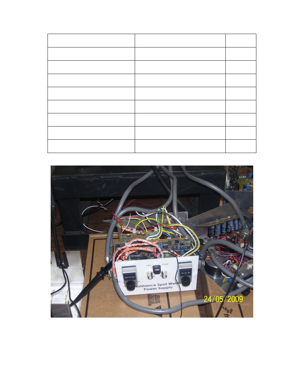
50
• Rail-Rail Op-Amp LMC6482
MOSFETs
IXFN 200 N07
4
MOSFET driver
IR2184
1
Voltage regulator
MC78L00
1
High Side Current Sense Monitor
ZXCT1010
1
Hall-Effect Sensor
A1302
1
PWM Chip
SG3525A
1
Timer Chip
Dual Retriggerable MC14538B
1
Analog Switch
Analog Multiplexer CD4053BC
1
Figure
3-15: RSW power supply modified unit

51
Chapter 4
4
Improved Consistency of Resistance Spot Welding via
Power Supply Control Strategy
This chapter and the following one will discuss the second part of my Ph.D. research
work, which is improving the consistency of RSW using the power supply designed in
our lab. In order to improve the consistency of RSW, three control modes have been
studied, open loop voltage control, constant current control and constant tip voltage
control. Open loop voltage control mode is the original control mode for resistance spot
welding, while constant current control mode is the present state of the art control
technology, due to its better performance with controlling the spot welding process.
Even with its better performance, it doesn’t overcome the problems resulting from the
changing of electrode geometry with age. With changing of electrode geometry,
particularly the mushrooming effect, constant current does not result in constant current
densities [59], which can lead to significant temperature and melting variations.
The means presently used to control the weld current density using constant
current control is to periodically increase the weld current set point over time [59] to
match the increase in electrode tip contact area [59]. However, this compensation
scheme works until the electrode tips become so heavily plated, oxidized, or cracked that
the overall heat balance is affected, which in turn decreases the weld quality. The best
solution to control the weld current density during the welding process is to use constant
tip voltage control, which automatically ensures constant weld current density, due to its
proximity to current density than weld current [59].
Other advantages for using constant tip voltage as a control mode for the welding
process, being ideal for welding round-to-round and round-to-flat parts without causing
weld splash. It is also ideal for welding parts with inconsistent co-planarity. It
automatically reduces weld splash caused by inconsistent part-to-part and electrode-to-
part weld heat contact area variability. It also automatically adjusts for variability in the
t
R A
product, which is used to calculate the heat density as shown in equation (4.1),

52
where for constant current control changes in the
/
t
R
A
ratio affect the weld heat density
[60].
(
)
2
2
/
(
/ )
d
t
d
t
Q
V t
R A
Q
I t R
A
≈
≈
(4.1)
where:
2
2
Weld heat density
Weld current squared
Weld voltage squared
Weld period time
Weld total electrical resistance
Weld heat contact area
d
t
Q
I
V
t
R
A
=
=
=
=
=
=
Therefore for this research, we chose to use constant tip voltage as one of the
control modes for our PID controller and compare it to the open voltage control mode
and the constant current control mode in improving the consistency of RSW. This
chapter introduces constant tip voltage control mode as one of the control modes for the
spot welding process and compare it to the other two control modes, which proved to
give better performance than both of them. These three control modes are discussed and
implemented in this chapter. A comparison between the three control modes will be
discussed in the last section of the chapter.
4.1 RSW Control Modes
4.1.1
Open Loop Voltage Control Mode
The open loop voltage control mode is to control the PWM duty cycle (D) as a constant
to achieve the theoretical constant open circuit voltage (the theoretical voltage before the
output impedance of the power supply). Note that with the PWM duty cycle being
assigned as a constant, the PID controller is no longer necessary. Figure
4-1 shows the
diagram of the open-loop voltage control mode.
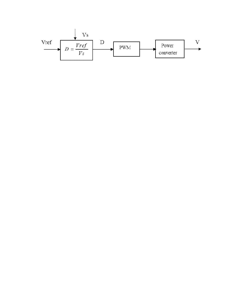
53
Figure
4-1: Block diagram of open loop voltage control mode
Under the open loop voltage control mode, the desired output voltage is given as a
voltage reference Vref. and the duty cycle D is calculated as the ratio of the desired
output voltage divided by the source voltage (which is the open circuit battery voltage for
our power supply). Then the calculated duty cycle D is implemented to generate the
PWM signals, which control the power converter for the power supply.
4.1.2
Constant Current and Tip Voltage Control Modes
The constant current and tip voltage control modes are closed loop control modes, where
the weld current or the tip voltage is being used as an input to the PID control to control
the duty cycle. Under the closed loop current and tip voltage control modes, the welding
current and the tip voltage respectively are regulated as a constant, and the duty cycle
adjusts to compensate for variations in the load resistance and/or changes in line
impedance.
4.2
Experimental Procedure
In order to determine which of the three modes will give the most consistent spot welds, a
series of welds were conducted and the variance of the nugget diameter was measured for
each of the control modes.
The basics steps in this procedure are:
• Ramp test to determine the basic operating variables, i.e., weld time, and duty
cycle, that are needed to perform the open loop voltage control mode.
• 100 welds for open loop voltage control mode are performed and the mean nugget

54
diameter is calculated.
• From the open loop voltage control mode series of welds, the average tip voltage
and average current is calculated and is used as an initial guess for the set points
for the constant current and constant tip voltage control modes.
• The PID controller gains are tuned for each of the set points.
• Set points are adjusted to give the same mean nugget diameter as the open loop
voltage control mode. For valid comparison of the variances of nugget size, it is
important that the mean nugget size is held constant. As discussed earlier, the heat
input during resistance spot welding is a function of the resistance. Further, the
trajectory of the resistance is a function of the control strategy. Figure
4-3
compares typical time trajectory of the resistance for constant voltage and constant
current welds. Even if set-points could be determined that delivered identical
heats, they could not be expected to produce identical welds. The figure shows
the resistance is dropping to zero at the end of the weld time, which is due to the
drop of the tip voltage to zero and having a zero offset for the current signal at the
end of the weld.
• 100 welds are performed for each of the constant current closed loop control mode
and constant tip voltage closed loop control mode, and the mean nugget diameter
is calculated for each.
• The nugget diameter variance is calculated to perform the comparison between the
three control modes in improving the consistency of the RSW process.
In order to determine the accuracy of our results, we calculated the variances of
40 random numbers that were generated from both a normal and uniform distribution,
both with variance 1, 500,000 times. This generated the probability density function
(PDF) shown in Figure
4-2. We then repeated the experiment with 100 random numbers.
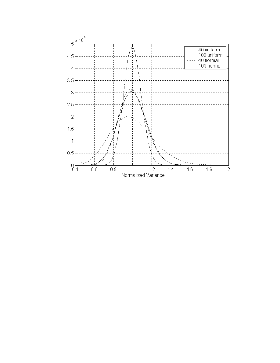
55
Figure
4-2: Probability density function for determining number of experiments
From this we see that if our results are uniformly distributed we would have a
90% chance of our variance estimate being within +/-24% of the real answer. However,
if our results are normally distributed we would only expect to be within 37% of the
correct answer. If we were to perform 100 repetitions we would expect an accuracy of
14.9% and 23% for uniformly and normally distributed data, respectively. We expect our
experimental data to have a distribution between that of normal and uniform, as we
expect a distribution to be similar to Gaussian but recognizing that there are hard physical
constraints on maximum and minimum welds that can occur as with a uniform
distribution.
4.2.1
Experimental Setup
The experimental setup includes a small scale resistance spot welding (SSRSW) head
from Unitek Peco Model 80, electrical current and tip voltage sensors, the developed DC
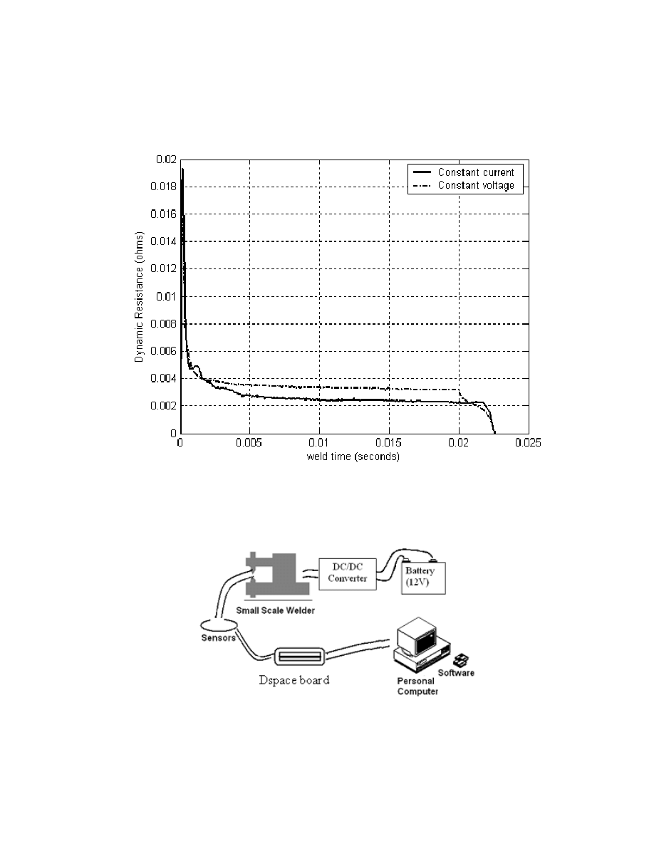
56
power supply, a data acquisition system and a PC computer. Figure
4-4 shows the block
diagram of the setup
[18].
Figure
4-3: Typical dynamic resistance for constant voltage and current control
modes
Figure
4-4: Block diagram of experimental set-up
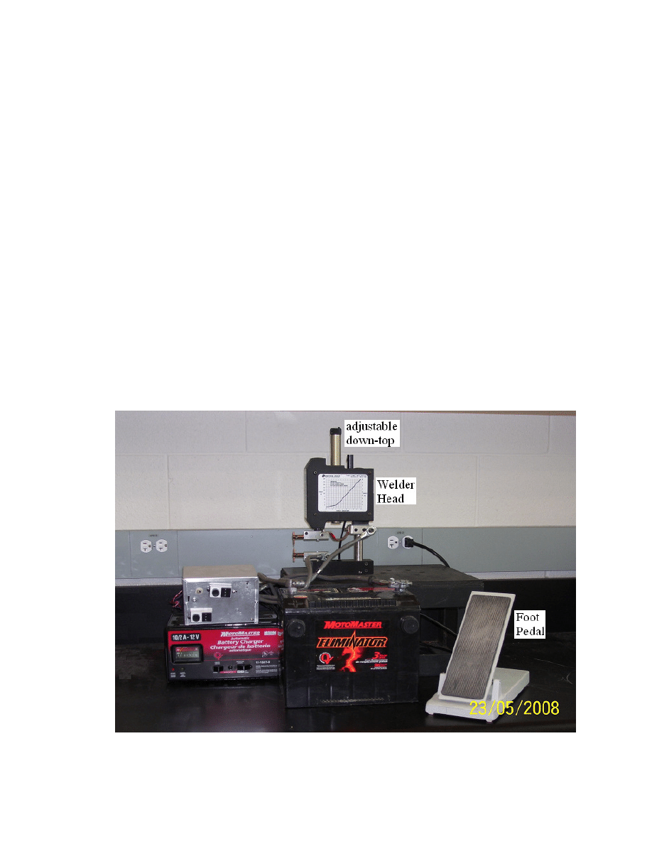
57
The electrodes used in the test are ES0402-RWMA2 - (COPPER CHROMIUM
ALLOY - 83B Rockwell hardness, 85% conductivity), which are widely used for welding
of steels, nickel alloys and other high resistance materials. The dimensions are 1/8−inch
(3.18mm) diameter, 5/4−inch (31.75mm) long, and the tip electrode diameter is
1/16−inch (1.59mm). The whole welding process is semi-automatically controlled. The
weld force is applied to squeeze the upper electrode to the lower electrode.
A Model CP cable foot pedal is used to apply electrode force after two overlapped
coupons are manually placed between the opposing electrodes. The Model CP cable
pedal pivots under the heel for optimum force control. It is equipped with an adjustable
down- top, which prevents the application of excess force. It is rated at 25 pounds, and
can be used with Unitek Peco Model 80 weld head. When the force applied by the pedal
reaches the preset value, the welding current is generated through the electrodes and the
workpieces by the DC power supply. Figure
4-5 shows the welder head, the force
adjustable down-top and the foot pedal for the SSRSW system.
Figure
4-5: Welder head, force adjustable down-top & foot pedal
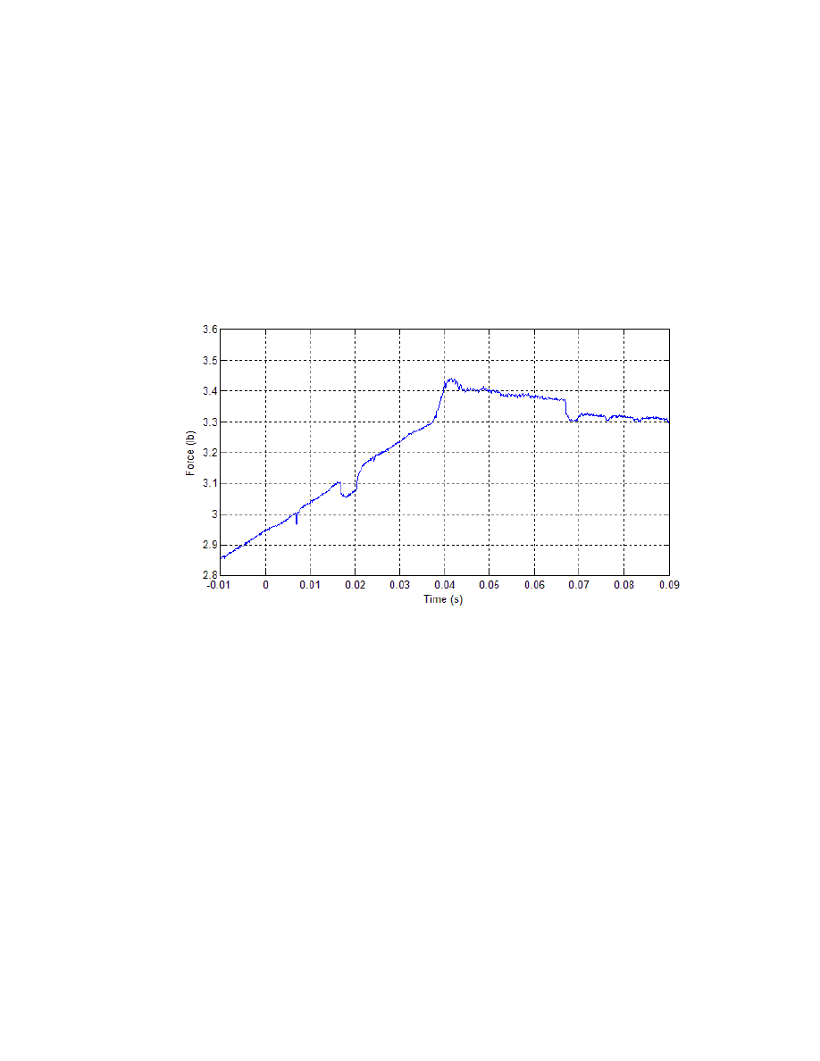
58
The electrode force can be adjusted either from the adjustable down-top located
on the top of the welder head or from the two bottom screws located at the bottom of the
foot pedal. Figure
4-6 shows the typical forces generated when the electrodes close
where t=0s represents the time the welder force trigger was set. The force would start at
the specified force but would continue ramping up to a random force and settles there at a
random time. In the graph, the force was adjusted close to 2.8lb and started to ramp up
close to 3.3lb, and settled there at 40ms.
Figure
4-6: Electrode force
A load cell was used to help calibrating the force. Moreover a delay of 0.1
seconds was added at the start of the welding process. The force was adjusted by
adjusting the length of the cable attached to the foot pedal to achieve desired force when
foot pedal fully depressed. Doing that, we were able to keep the force constant at the
adjusted force from the beginning of the weld at 0ms till the end of the weld time, which
is 20ms in our case, as shown in Figure
4-7. In this figure the force was adjusted to stay
close to 4.5lb, and as shown in the graph, the force stayed constant close to 4.5lb from the
beginning of the weld time (t=0s) till the end of the weld time (t=20ms).
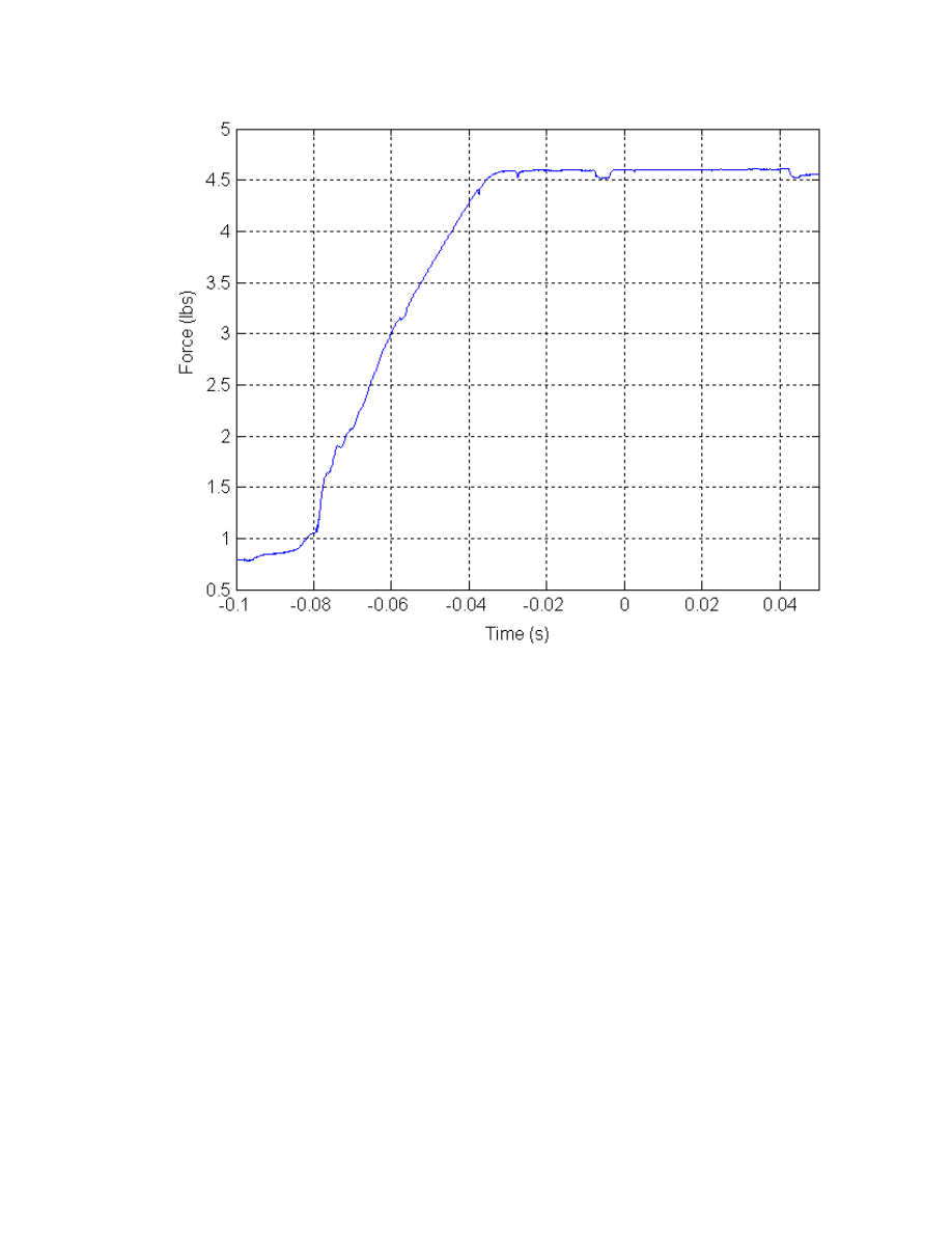
59
Figure
4-7: Adjusted electrode force
Current and tip voltage sensors are used to measure the welding current and tip
voltage transmitted to the PC computer through the data acquisition system. The DS1104
controller board, which is a single-board simulator from DSpace, is inserted into the
computer. The software does the job of signal processing. The power supply is a pulse
width modulated DC-DC converter. Thus its nominal output is given by the duty cycle
times the maximum voltage 13.5V.
For measuring the nugget diameter, the overlap area of the assembled test sample
should be three-quarters of the coupon length. Two adjacent spot welds should be placed
in the overlap area. The second weld nugget (B) should be marked to differentiate from
the first one (A). The material being welded was 2 identical 0.152mm gauge stainless
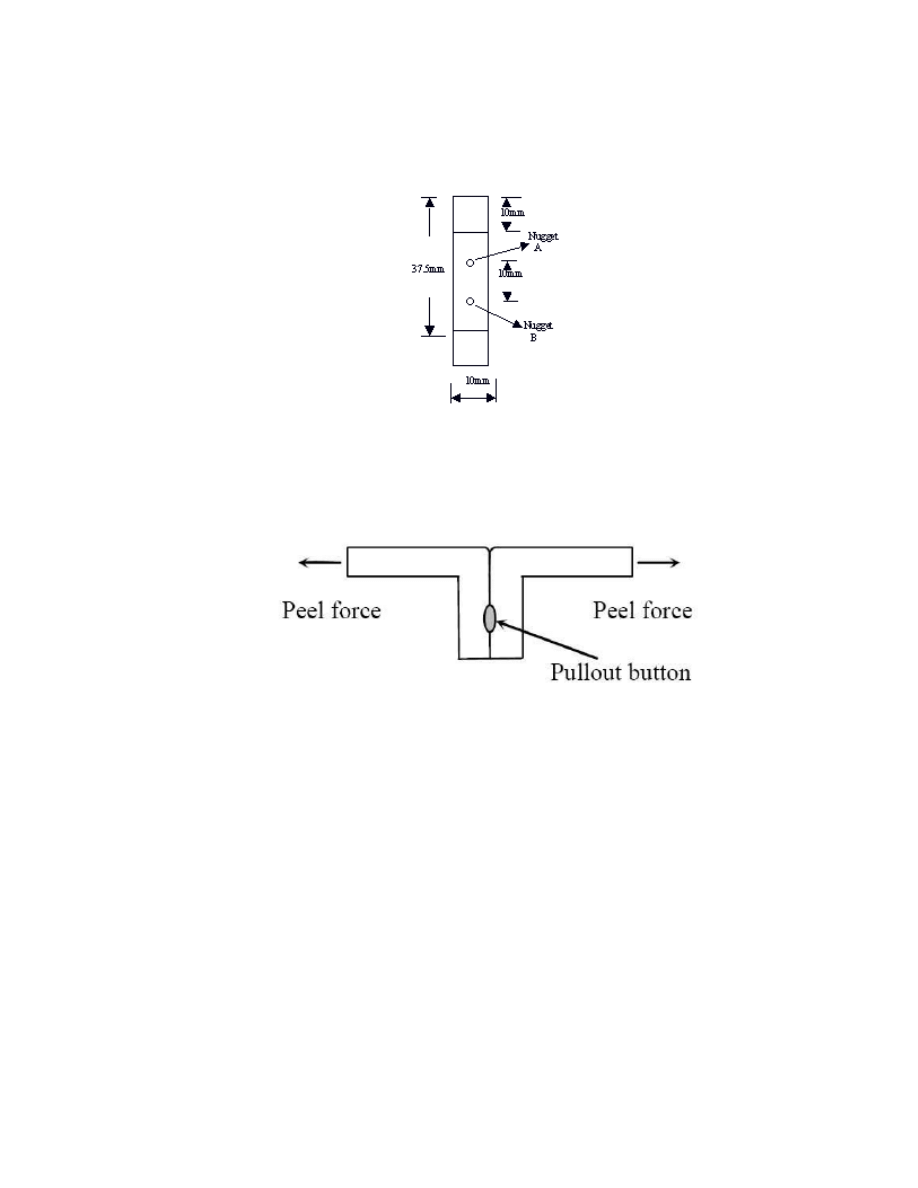
60
steel coupons with dimensions of 37.5mm × 10mm. Figure
4-8
shows the welding
samples for measuring the nugget diameter.
Figure
4-8: Peel test sample
4.2.1.1
Peel Test
Figure
4-9: Peel test for measuring nugget diameter
The peel test is a simple test for measuring the nugget size (Figure
4-9)
[56],
[57]. When
welding samples, the second weld nugget (B) should be marked as shown in Figure
4-8.
In the peel test, the sheets are first separated on one end of a lap joint, and the roller rolls
up one sheet while the other is gripped. As the roller rolls over the weld, half of the
workpiece is torn off at the weld and a weld (A) button is left.
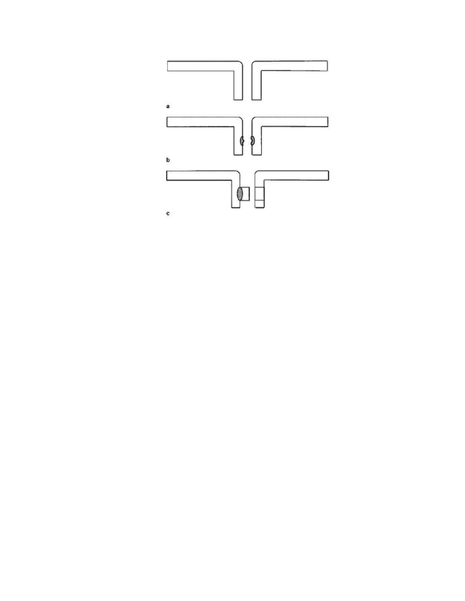
61
Figure
4-10: Schematic showing joint failure modes during peel test
With continued peeling, the whole workpiece is torn off and another weld (B)
button is left. The nugget size can be estimated and recorded as a parameter for welding
quality by measuring the diameter of pullout button (B). If the button shape is irregular,
the button diameter is determined by taking an average of the maximum and minimum
dimensions. Microscope is used to see the nugget diameter fore each of the pullout
buttons (B) for each welding sample, and an enlarged photo as shown in Figure 4-11 is
taken for each to be able to measure the diameter fore each nugget.
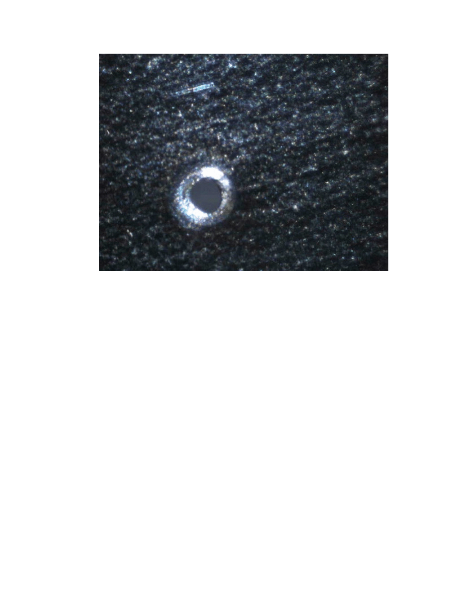
62
Figure
4-11: Nugget diameter picture for one of the welding samples
Various failure modes can usually be observed during the peel testing of welded
joints, namely:
a)
Interface failure,
b)
Weld failure, and
c)
Button pullout as shown in Figure
4-10
[29].
Interface failure is due to lack of bonding or only weak bonding between sheets.
Once a weld nugget formed, joints generally failed through the nugget when the nugget
diameter is small or by a button pullout when it is above a certain size, which is called
weld failure or button pullout. The failure modes usually serve as a rough indicator of
whether a specimen size is adequate.

63
4.3
Ramp Test for Open Loop Voltage Control
A”Weld Lobe” is used to describe the condition of weld current, force and time, which
allows satisfactory welds to be created. The weld lobe is usually determined through
“Lobe Tests”. Lobe testing is an effective aspect of weldability study. It generally refers
to the capability of with standing load, or for revealing important weld characteristics,
such as weld nugget diameter
[26].
On the other hand, performing a Lobe test is a time and money consuming
process, where lots of spot welds with different welding parameters such as force, weld
time, power, etc. need to be done and analyzed before determining the best operating
point, which uses lots of welding materials as well as time for performing the welds and
calculating the results.
Therefore in order to determine the correct operating conditions in this research, a
“Ramp Test” [50] was used. A ramp test is a new method that helps in reducing time and
welding materials in obtaining a good operating point for welding parameters. The test
requires an initial estimate of what the weld current and weld time should be. The
current is then linearly raised from 0 amps to 150% to 200% of this current over a period
of approximately 30% to 80% longer than the expected weld time. This excess current
and time should ensure that an expulsion occurs during this weld. The exact time of
expulsion and corresponding weld current are determined by looking at measurements of
the weld current and weld voltage. The weld time is set equal to this expulsion time and
the weld current set point is set equal to half the expulsion current, or, equivalently, the
average current prior to expulsion.
Unfortunately, our welder could not easily provide double the expected current set
point so we were not directly able to apply this method. Also our goal was to find an
open circuit voltage set point instead of a current set point. Thus we modified this
approach in two respects.
1)
Instead of applying a linearly increasing current, we applied a linearly increasing
open circuit power supply voltage.
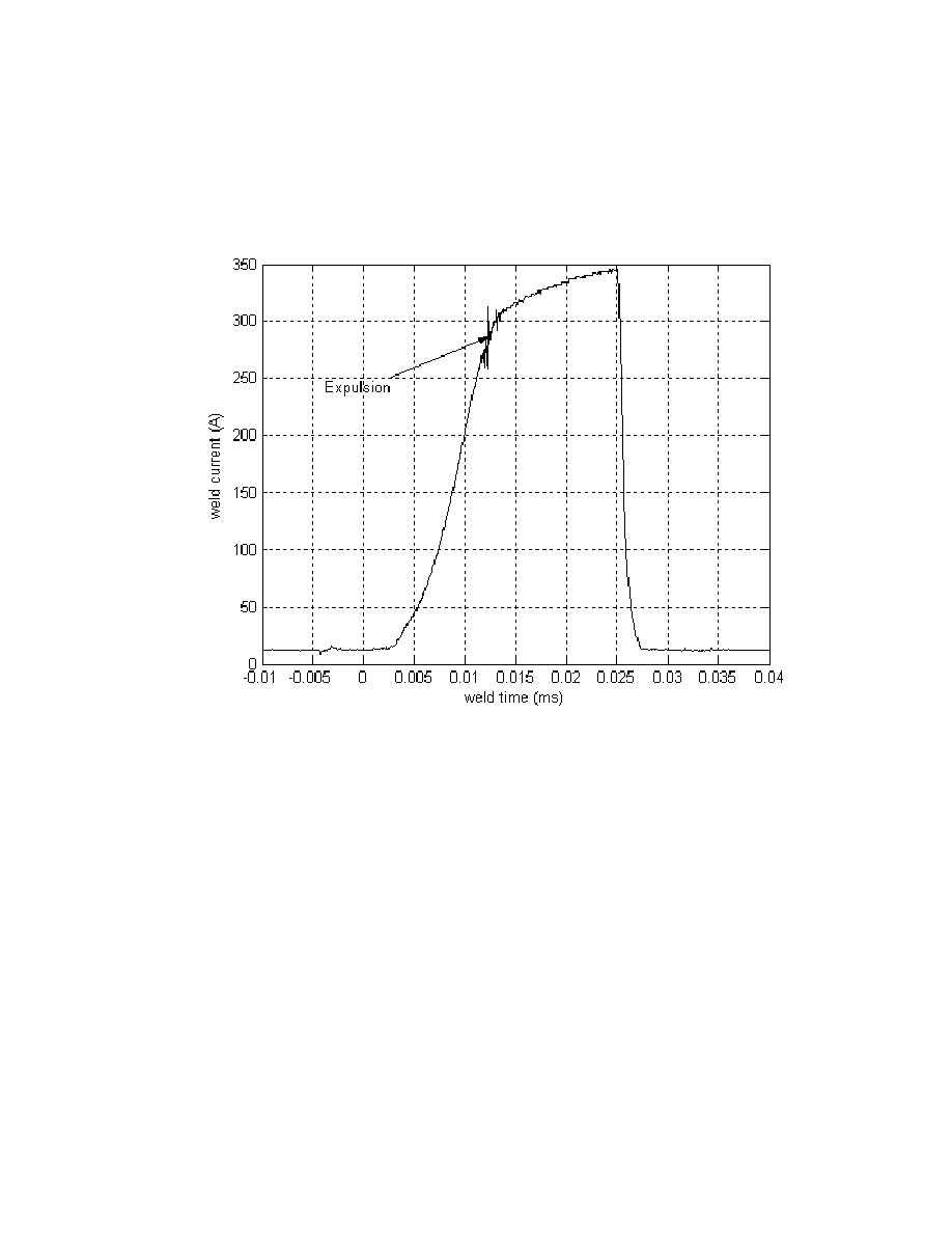
64
2)
Instead of ramping up from zero to double the expected voltage, we started from
30% of the expected set point to 50% greater than the expected set point. The
weld set point is still taken as the average duty cycle prior to expulsion.
Figure
4-12: Weld current ramp from 30% to 80% duty cycles
For this research, the following were used in the weld study, using the ramp test
method: force of 4lbs, weld time of 25ms and duty cycle rising from 30% to 80%. The
force was set at 4lbs as this was the maximum force where the power supply could
provide energy fast enough to produce expulsions The force was used throughout all the
experiments that were done in improving the consistency for RSW in this research.
• Expulsion was reached at approximately 12ms with duty cycle of 54% as shown
in Figure
4-12. The 12ms should of taken as the weld time for the operating point,
and the duty cycle should been set to 42% (the starting duty cycle + the final duty
cycle, all divided by 2, (30+54)/2. Figure
4-12 shows the weld current starting

65
form almost 10amp, which is due to the fact that our current sensor wasn’t zeroed,
so current sensor readings started from10amp, which is actually representing
0amp for the actual weld current signal.
For large scale spot welding, a rule of thumb is that a reasonable nugget should
have a diameter close to 80% of the electrode size. Our nuggets were much smaller than
this. Thus after finding a workable operating point with the ramp test, we did a grid
search and few experiments for the best weld time that will give us the largest diameter
for our spot welds, without having expulsions at the spot welds. We were able to achieve
that with 20ms weld time, and 42.5% duty cycle. The result was still quite small relative
to the electrode diameter and is a significant difference in the small scale and large scale
resistance spot welding process.
Table
4-1 lists the mean nugget diameter for each of 50%, 45%, 42.5% & 40%
duty cycle. We thus determined the operating point for open loop voltage control mode
to be 42.5% duty cycle, 20ms weld time and 4lb force.
Table
4-1: Different duty cycles weld nugget diameters
Duty Cycle
Mean nugget diameter
Expulsion
50%
0.349mm
40% of the welds
45%
0.337mm
30% of the welds
42.5%
0.302mm
No expulsion
40
0.280mm
No expulsion
100 welds for the open voltage control mode were undertaken with the operating
condition of the specified operating point; the mean nugget size 0.302mm was measured.
In addition, the weld currents & tip voltages were measured during these welds and a
mean weld current & tip voltage was determined to be 315A & 1.035V respectively,
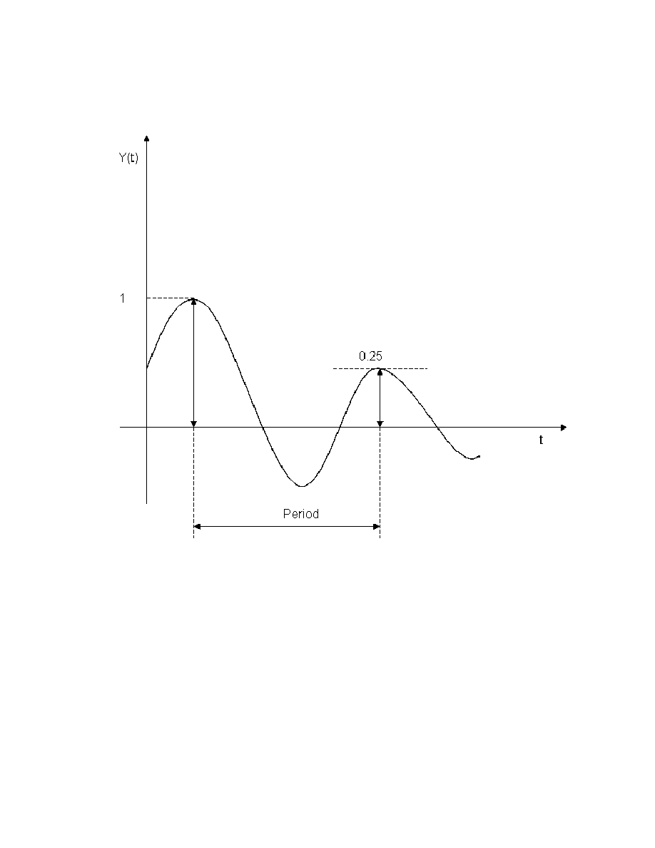
66
which were used as the set points in performing the closed loop experiments for constant
current control mode and constant tip voltage control mode.
Figure
4-13: Quarter decay ratio
4.4
PID Tuning for Constant Weld Current & Tip
Voltage Control Modes
Two PID controllers need to be tuned to implement the constant current and constant tip
voltage control modes. In order to achieve this, a Ziegler-Nichols tuning method
[53]
was used. Ziegler and Nichols gave two methods for tuning the controller. In the first
method, which is the method we applied to design our PID controller, the choice of
controller parameters is based on a decay ratio of approximately 0.25, which means that
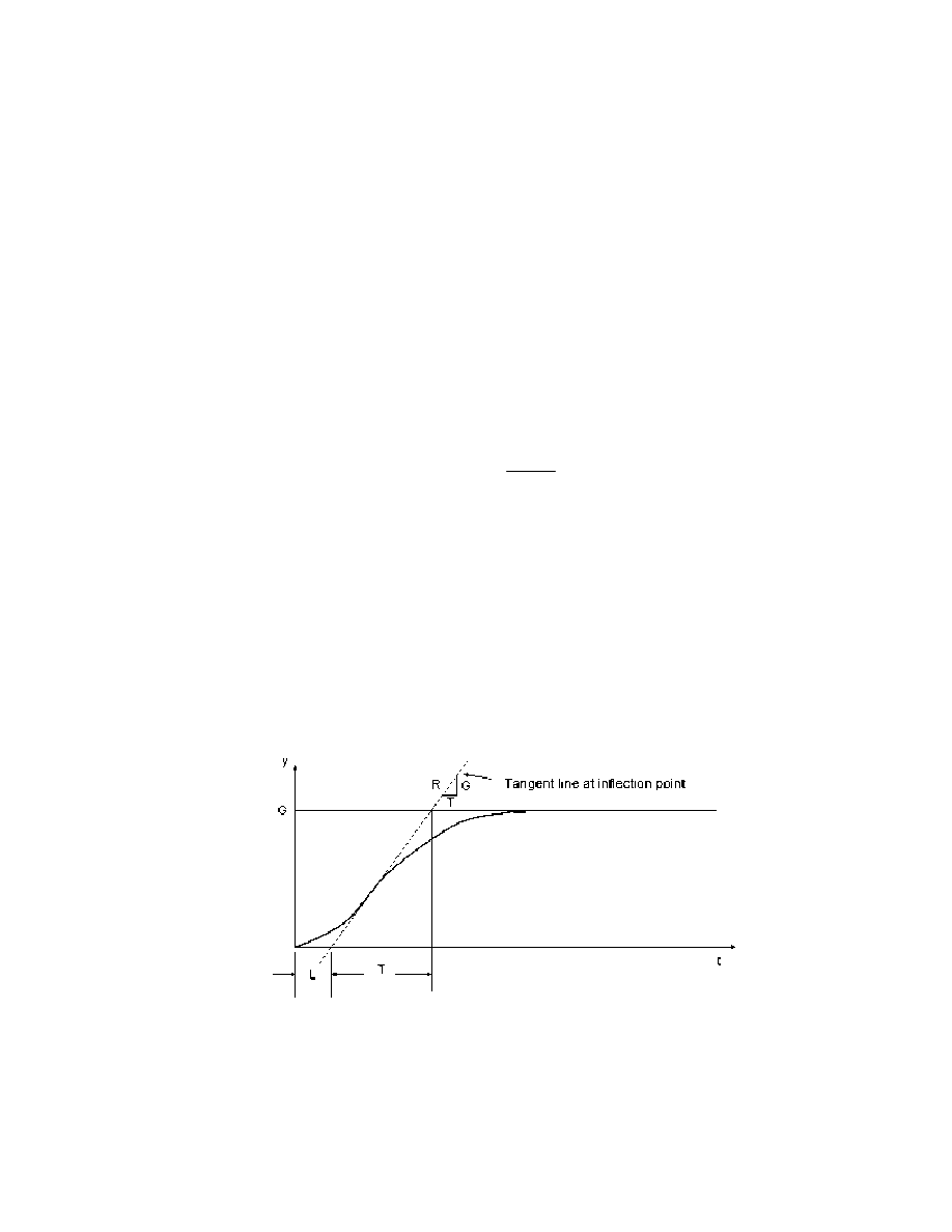
67
the dominant transient decays to a quarter of its value after one period of oscillation, as
shown in Figure
4-13. A quarter decay corresponds to
0.21
ζ
=
and is good compromise
between quick response and adequate stability margins.
Ziegler and Nichols recognized that the step response of most process control
systems has the general S-shaped curve shown in Figure
4-14, which is called the process
reaction curve and can be generated experimentally or from dynamic simulation of the
plant. For designing our PID controller, the welding samples from the open voltage
control mode were used to generate this curve. The shape of the curve is characteristic of
high-order systems but may be approximated by
( )
1
d
sT
Ke
F s
s
τ
−
=
+
(4.2)
which is simply a first-order system plus a transportation lag. The constants in the above
equation can be determined from the step response of the process. If a tangent is drawn
at the inflection point of the reaction curve, then the slope of the line is approximately
R=K/τ
, where K=G/∆u, where ∆u is the size of the step and G is the change in the output
following the step. The intersection of the tangent line with the time axis identifies the
time delay
d
L
T
=
.
Figure
4-14: Ziegler-Nichols S shape curve
The regulator parameters suggested by Ziegler and Nichols are show in Table
4-2.

68
Table
4-2: Ziegler-Nichols tuning parameters
Type of Controller
Optimum Gain
PID Gains
PID
1.2
,
2 ,
0.5
P
I
D
K
T
L T
L
RL
=
=
=
,
,
P
P
P
I
D
P
D
I
K
K
K
K
K
K T
T
=
=
=
In order to measure these quantities for the welder system in this research, 20 welds were
performed with duty cycle set to 45% at the first 18.6ms of the weld and then decreased
to 39.5% until 23.6ms. The resulting welding currents and tip voltages were recorded
and then averaged. Two transfer functions were designed as the following equations, one
representing the tip voltage and the other representing the weld current.
( )
1
( )
1
I
V
sTd
WC
I
WC
sTd
TV
V
TV
K
e
F s
s
K e
F s
s
τ
τ
=
+
=
+
(4.3)
(45)
(39.5)
(45)
(39.5)
45 39.5
5.5
(45)
(39.5)
(45)
(39.5)
45 39.5
5.5
WC
TV
I
I
I
I
I
K
D
V
V
V
V
V
K
D
−
−
∆
=
=
=
∆
−
−
−
∆
=
=
=
∆
−
(4.4)
where
•
I
∆
&
V
∆
are the difference in weld current and tip voltage respectively, from value
at 18:6ms,
•
D
∆
is the difference in duty cycle from 45%,
• I(45) & V(45) are defined as the steady state weld current and tip voltage
respectively, when duty cycle is 45%,

69
• I(39.5) & V(39.5) are the mean weld current and tip voltage respectively, when
duty cycle is 39.5%,
•
I
Td
&
V
Td
are the first moments after 45% duty cycle that the weld current and the
tip voltage have changed,
• The time constants
I
τ
&
V
τ
are approximately given by the time the weld current
and tip voltage respectively, have reached 63% of their total change.
Figure
4-15 & Figure
4-16 show the plot of step test result for calculating the
transfer functions for weld current and tip voltage, and Table
4-3 shows the values for the
transfer function parameters.
Table
4-3: Weld current and tip voltage transfer functions parameters
Transfer functions parameters
Values
WC
K
2.79
TV
K
0.0184
I
Td
4
2 10
−
×
V
Td
4
1 10
−
×
I
τ
4
2.8 10
−
×
V
τ
4
2.4 10
−
×
I(45)
210A
I(39.5)
195A
V(45)
0.87V
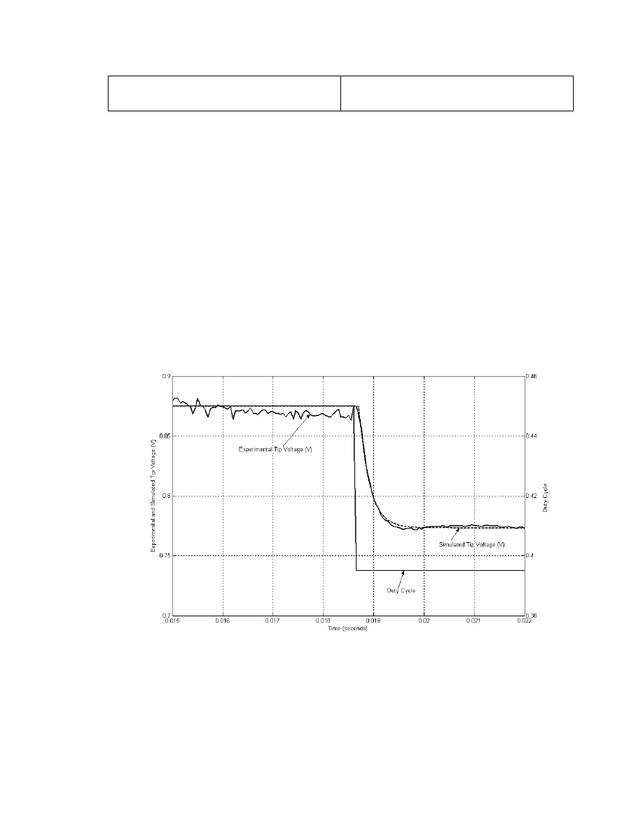
70
V(39.5)
0.77V
The final tuning of the controller can be done manually by the process operator to
yield the “best” control. In order to achieve this final tuning, the transfer function
identified above was implemented in Simulink as shown in Figure
4-17, where α is a
variable that is set to 1 when using constant current control mode, and is set to 0 when
using constant voltage control mode. The tuning of these controller gains resulted in little
modification of these initial values to achieve an overshoot of 10.9% for pure tip voltage
control and 5.1% for pure current control with fastest rise time for both (Figure
4-18 &
Figure
4-19). The corresponding gains for constant current control mode are K
Pi
= 0.125,
K
Ii
= 750, and K
Di
= 7.6325e-5, and for constant tip voltage control mode are K
Pv
= 12.5,
K
Iv
= 1.25e5, and K
Dv
= 0.0098.
Figure
4-15: Tip voltage step test
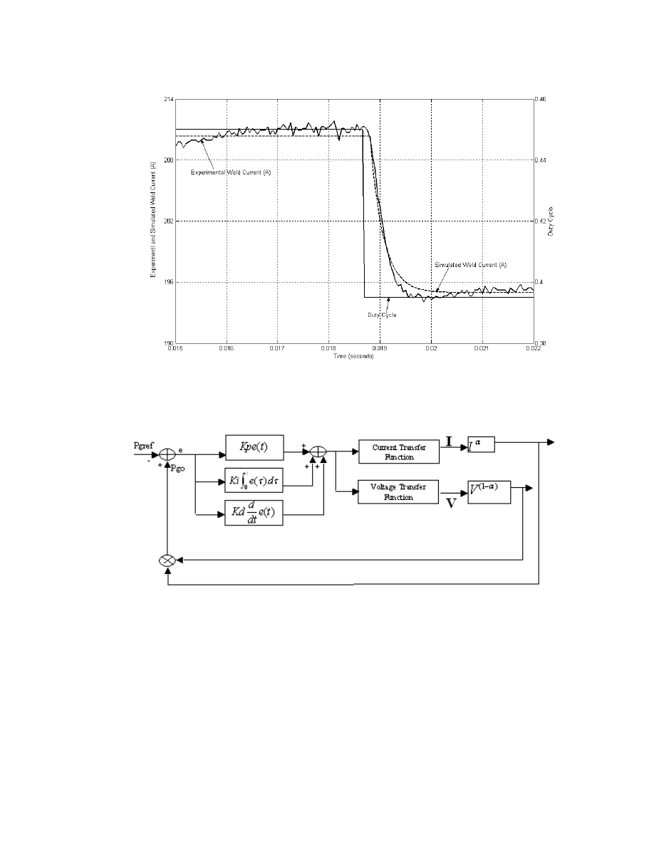
71
Figure
4-16: Weld current step test
Figure
4-17: PID Simulink model
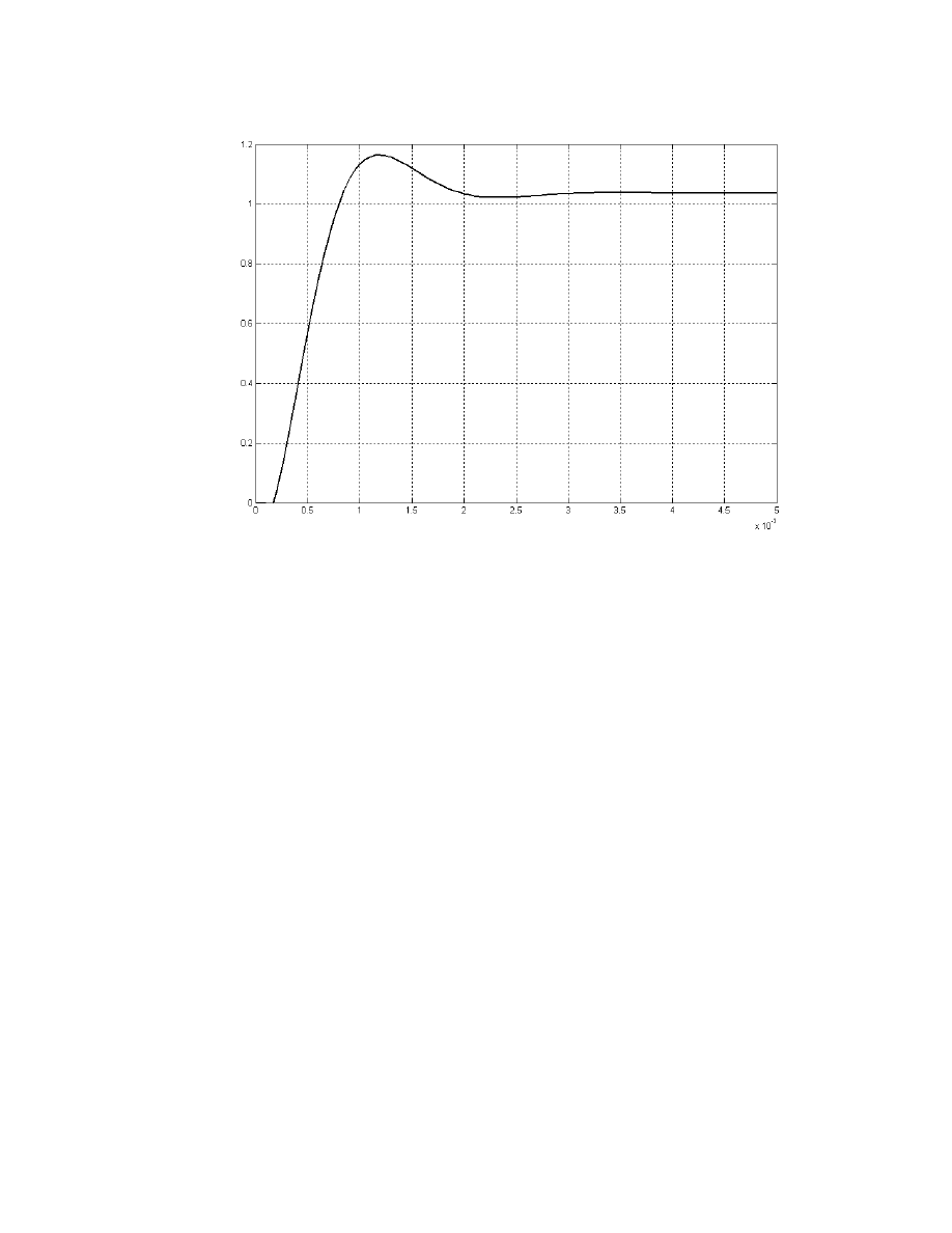
72
Figure
4-18: PID controller tuning for constant voltage control mode
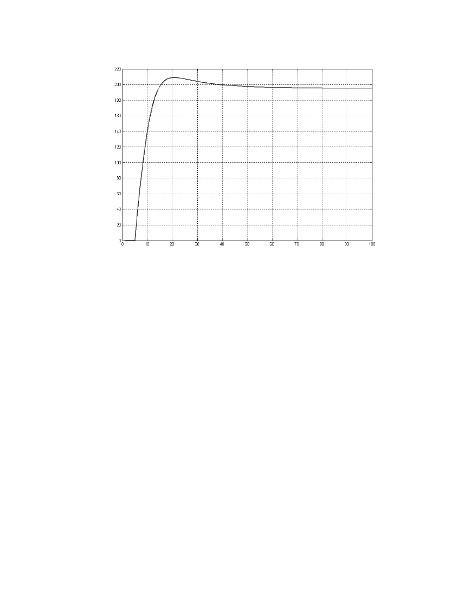
73
Figure
4-19: PID controller tuning for constant current control mode
4.5
Open Voltage, Constant Current & Constant Tip
Voltage Control Modes Comparison
Hundred welds were done for each of the constant current control and constant tip
voltage control, using the set point calculated for each from the open loop voltage control
experiment and with the tuned PID gains. Mean nugget diameter was then calculated
with a slight change to the set points, to ensure that the set points chosen for each of the
weld current and tip voltage will give the same or relatively close nugget diameter size as
the one calculated from the open loop voltage control, which is 0.302mm. As a result the
final set point for each was 316A and 1.036V respectively. These set points gave nugget
diameter size of 0.3005mm for constant current control, and 0.301mm for constant tip
voltage control.
Based on the experimental data from the welding tests for each of the control
modes, further statistical analysis has been performed. The variance for the nugget size
has been studied. It is used to evaluate the general effect of each control mode on the

74
welding quality. The smaller the variance, the less dispersion of the samples, and more
consistent the weld quality. The variance of nugget size is expressed as:
2
2
1
1
ˆ
(
)
n
a
i
i
A
A
n
σ
=
=
−
∑
(4.5)
where
i
A
is the diameter of the nugget sample i, ˆ
A
is the mean of the nugget diameters
and
2
a
σ
is the variance. Table
4-4 gives the variance of nugget size for each of the three
control modes.
Table
4-4: Variance in nugget diameter
Control Mode
Variance
Open Loop Voltage Control Mode
4
2
4.0 10 mm
−
×
Constant Current Control Mode
4
2
3.3 10 mm
−
×
Constant Tip Voltage Control Mode
4
2
2.5 10 mm
−
×
Figure
4-20 illustrates the variance of nugget size for each of the control modes.
It is obvious that the variance for both of constant current and constant tip voltage control
modes is much smaller than the open voltage control mode, with the constant tip voltage
control mode giving the smallest of both. In other words, when the controller is under the
constant tip voltage control mode, we get the most consistency in the spot welds nugget
diameter.
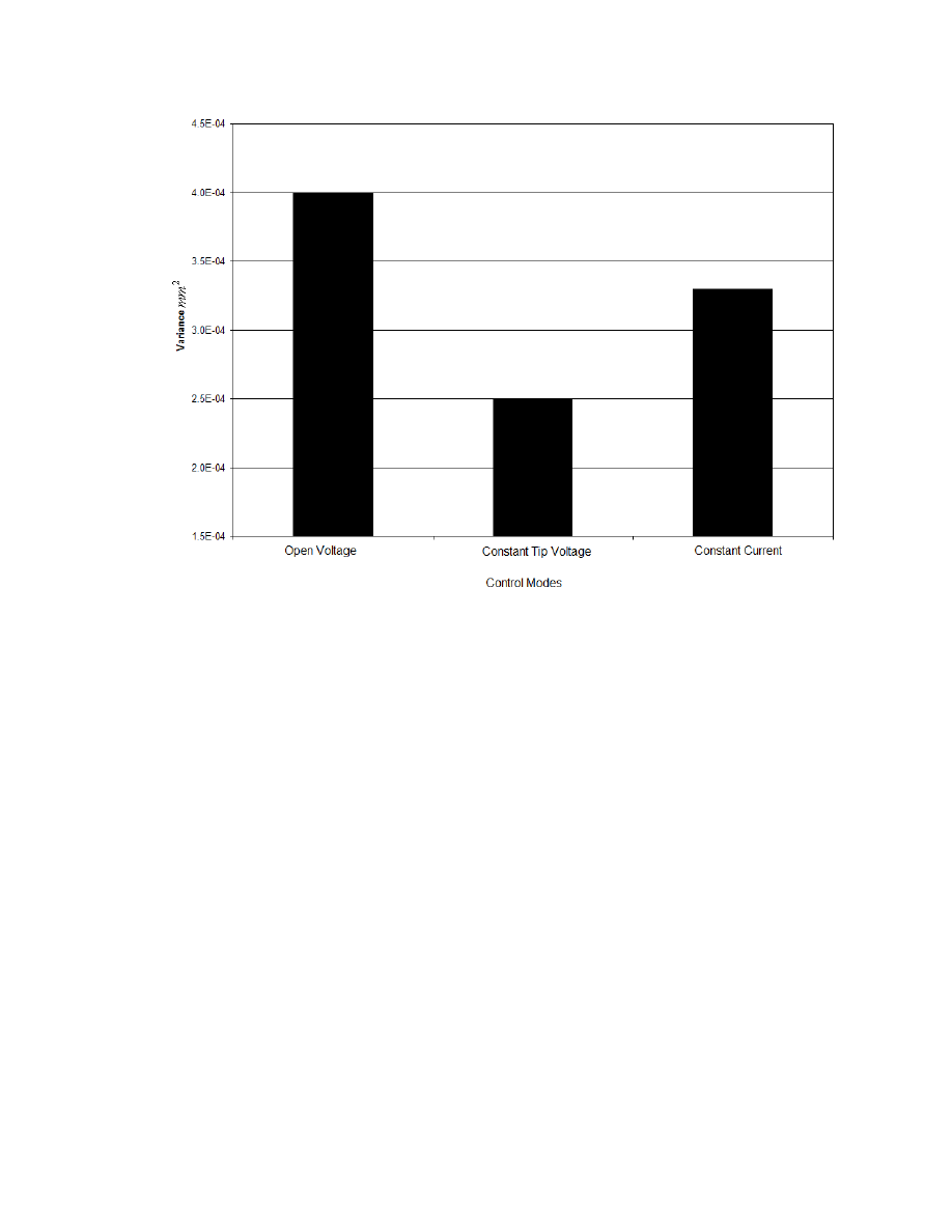
75
Figure
4-20: Variance comparison in nugget diameter
To verify the accuracy of our results, histogram plots were done for each of the
three control modes 100 experimental data. The plots showed that our data is normally
distributed; therefore our variance result is within 23% of the real answer, according to
the PDF that was generated earlier in this chapter.
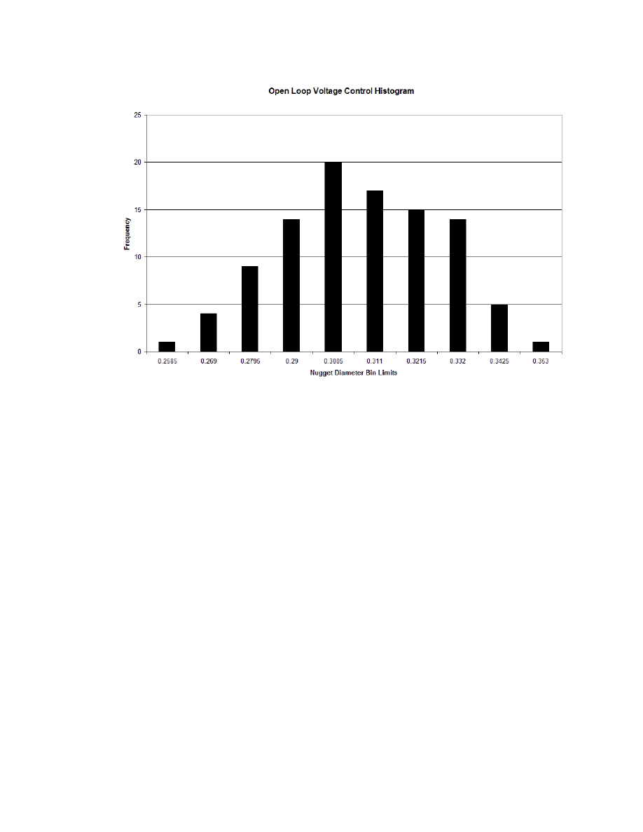
76
Figure
4-21: Open Loop Voltage Control Histogram
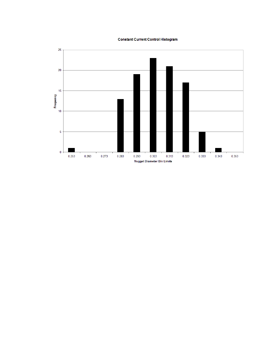
77
Figure
4-22: Constant Current Control Histogram
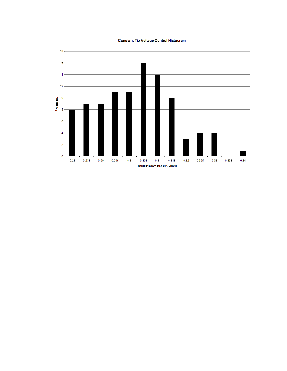
78
Figure
4-23: Constant Tip Voltage Control Histogram
4.6
Conclusion
Resistance welding power supply controls come in two flavors, closed loop or open loop.
In this chapter we were able to implement both modes for our RSW power supply, with
using two different types of feedback to our controller, weld current and tip voltage. We
were also able to use the nugget size diameter measurements to compare the three
different control modes, which indicated that constant tip voltage control mode gave the
most consistent spot welds compared to constant current control mode and open loop
voltage control mode. This result helped us to proceed to implement the generic power
control mode for our power supply control, which is explained in the following chapter.
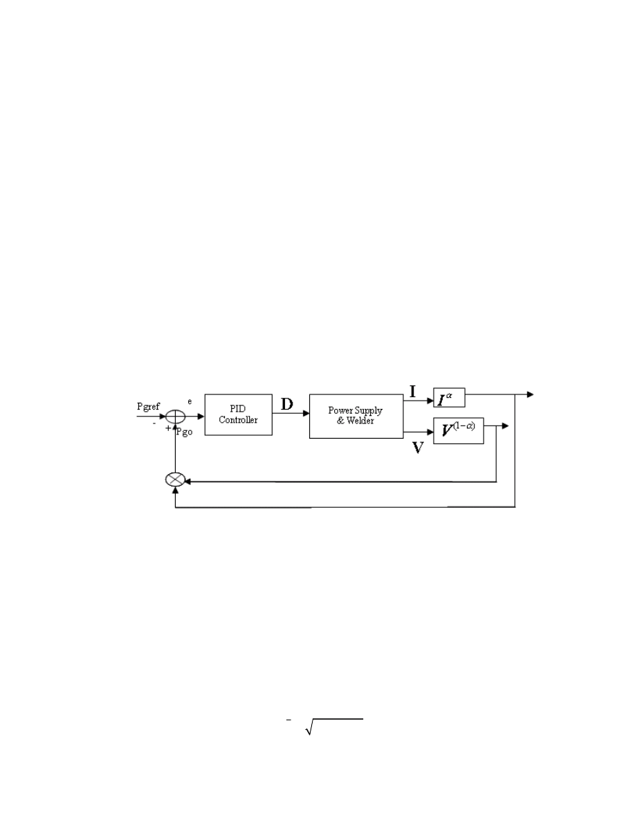
79
Chapter 5
5
Generic Control Mode for RSW
Few papers have been published indicating and comparing the resistance spot welding
weld quality with different control schemes
[5],
[17],
[46], including open loop control,
constant current control, constant voltage control and constant power control. After our
result of comparing open loop control with closed loop control using constant current and
constant tip voltage control modes, and after the improvement we achieved in the
consistency of the spot welds, we propose that any weighted geometric mean of voltage
and current is a viable control variable that can help in further improvements of the
consistency for RSW. Moreover, this approach unifies the existing constant current
(α=1), constant power (α=0.5) and constant voltage (α=0) strategies. Figure
5-1 gives the
block diagram of this generic weld power control scheme.
Figure
5-1: Generic power control mode
The geometric mean is an alternative means of finding average value that is more
appropriate when numbers vary over wide ranges or have different scales. Geometric
mean is similar to the arithmetic mean, except that instead of adding the set of numbers
and then dividing the sum by the count of numbers in the set, n, the numbers are
multiplied and then the nth root of the resulting product is taken. The geometric mean of
a data set [a1, a2, a3, ..., an] is given by:
1
1 2
1
( )
......
n
n
n
i
n
i
a
a a
a
=
=
∏
(5.1)

80
Thus the geometric mean of voltage and current is
( )
1
2
VI
, i.e., the square root of the
power. In statistics, given a set of data
1
2
,
,......
n
X
x x
x
=
, corresponding
weights
1
2
,
,......
n
W
w w
w
=
, the weighted geometric mean is calculated as:
1
1
1
n
i
i
i
w
n
w
i
i
x
x
−
=
=
∑
=
∏
(5.2)
In fact, power or some other weighted average of current and voltage can be used
to improve weld consistency. Based on this point, a weighted geometric mean of
variables V and I would be given by
1
V
I
α α
−
where 0
1
α
≤
≤ is the weighting.
Having defined this class of weld power controllers characterized by parameter α,
it remains to determine α that produces the best weld. It is expected that this value will
be strongly dependent on the geometry of the weld parts and characteristics of the power
supply used. One approach to find the best α is to define the best as the most consistent,
i.e., the one that has least variance in the heat delivered. This idea generates a simple
optimization problem based on the model of Figure
2-2. During weld setup, when the
basic settings for weld power, weld force and weld time are determined, additional data
could be collected that would allow the weld engineer to identify both nominal values for
the resistances, as well as measures of the uncertainty or variability of these values. This
could be as simple as maximum and minimum values, or variances. With this
information, a corresponding uncertainty of Q as a function of α could be calculated. The
α
that minimizes this variability would then be a reasonable choice for use in a
production environment. An alternative strategy would be to empirically determine the
weighting that produces the most consistent nugget size or strength. In next section we
pursue this strategy for one specific weld geometry and power supply to show the
potential for this approach.
The above approach was used by Jing Bai
[18],
[44] for her master’s research
work for improving the consistency for RSW. For her work a PI controller was used with
nominal voltage as a feedback with the weld current. The results demonstrated that a

81
40% weighting on the nominal voltage produced the most consistent welds. With this
control variable, substantial improvement in variance in nugget size and weld strength
compared with constant current control was achieved for each α value.
After introducing constant voltage control mode in chapter 4 using the tip voltage
as a feedback to the PID controller, and comparing it to open voltage control and constant
current control, which demonstrated better results than both, the generic power control
mode is implemented. For completing the second part of my Ph.D. research work, the
generic power control mode is implemented, using a PID controller with the tip voltage
as feedback with the weld current, and then repeated using the nominal voltage as
feedback for the PID controller with the weld current. A comparison between both
results will be made.
For Jing Bai’s work, nugget diameter and weld strength were both used to
validate our new approach for improving the consistency for RSW, but since the results
for the tensile test (weld strength) were consistent with the weld diameter but more costly
to perform, they were not repeated. Therefore only nugget diameter will be used to
validate our approach for improving consistency for RSW for my work.
5.1 Generic Power Control Mode Using Tip Voltage with
Weld Current
This section will explain the control strategy design for improving the consistency of
RSW via power supply control strategy using the generic power control mode strategy as
well as the experimental analysis and results. A comparison of resulting voltage, current
and power curves for constant power, constant current and constant voltage control
schemes is discussed as well in this section.
5.1.1
Control Strategy Design
Based on the control model designed in Figure
5-1, a generic power control mode was
designed as follows:
( )
1
g
P
V
I
α α
α
−
=
(5.3)

82
As shown in Figure
5-1, the desired output power is given as a power reference (
gref
P
).
The system feedback is the power (
go
P ), which is the product of the voltage and current
(
1
go
P
V
I
α α
−
=
). In this study, the output voltage (V) was measured through the tip voltage
sensor, while the output current (I) was measured through the current sensor. According
to the error signal (
gref
go
e
P
P
=
−
), the PID controller changes the PWM duty cycle to
regulate the output power.
Table
5-1: The generic control and other control modes
α
1
go
P
V
I
α α
−
=
Generic power control
0
go
P
V
=
Constant voltage control
0.5
go
P
VI
=
Constant power control
1
go
P
I
=
Constant current control
Different control modes have different output effects. Figure
5-2 - Figure
5-4
illustrate the difference between the three standard control modes in the output variables,
where V stands for the output voltage, I the output current, and P the output power. As
shown in the figures, the large peak in each figure represents the 100% voltage set point
that is applied for the first 0.3ms of the weld time. This is done to allow the basic PID
controller with no modifications to be employed. Otherwise, the PID controller would be
significantly in saturation and nonlinear anti-windup strategies would be required.
Moreover the three figures show a step at the end of each signal, which is due to having
the step test discussed earlier turned on during these experiments to demonstrate the
dynamics of the closed loop system.
For the closed loop voltage control (
0
α
= ) and current control (
1
α
= ), the tip
voltage and welding current respectively are regulated as constant, and the duty cycle is
adjusted according to load resistance, and the power changes accordingly. In the constant
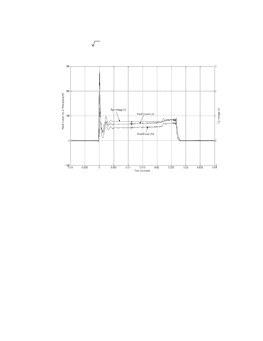
83
power control scheme (
1/ 2
α
=
), the tip voltage & weld current changes according to the
feedback power
go
P
VI
=
to keep the power constant.
Figure
5-2: Experimental results for constant tip voltage control mode (α=0)
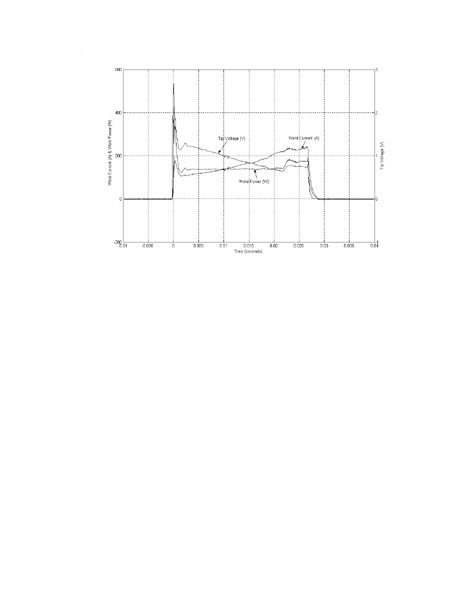
84
Figure
5-3: Experimental results for constant power control mode (α=1/2)
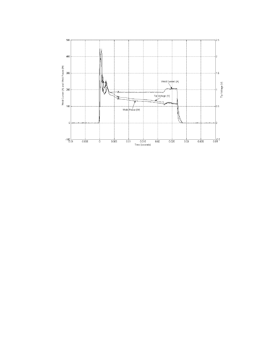
85
Figure
5-4: Experimental results for constant weld current control mode (α=1)
5.1.2
Application of Strategy to Welding 0.152mm Gauge
Stainless Steel
A series of welds were conducted and the variance of the nugget diameter was measured
for the 11 values of α from 0 to 1 by 0.1 increments. The same experimental setup used
for open voltage control, constant current control and constant voltage control as well as
calculating the nugget diameter will be used for the generic power control mode for each
α
value. The basic steps in this procedure are:
• Tune PID controller gains for each α.
• Identify set points for each α. For valid comparison of the variances of nugget
size, it is important that the mean nugget size is held constant (see
Chapter 4 for
more details).
• Perform a series of welds for each α and measure mean and variance for nugget
diameter.

86
5.1.2.1
Determining Set Point for Each α
The goal of this experimental work is to show how using different weighted means of
voltage and current as our controller variable affect the consistency of the welding
process. In order to make this comparison valid, it is necessary that the welds have the
same mean nugget size or close to what have been calculate for each of the open voltage
control, constant current control and constant voltage control. As mentioned earlier in
Chapter 4, the set points that gave the same mean nugget size for each of the constant
current and constant voltage control modes were 316A & 1.036V respectively. Therefore,
switched to the generic power control mode shown in Figure
5-1, the set points Pgo for
the other ten α values were evaluated as:
(1
)
(1.036)
(316)
Pgo
α
α
−
=
×
(5.4)
where α was changing from 0.1 to 0.9. Table
5-2 lists the corresponding set points at
each of the α values.
Table
5-2: Set points at different α values
α
Set Points Pgo
α
Set Points Pgo
0.0
1.036
0.6
32.11
0.1
1.85
0.7
57
0.2
3.3
0.8
100.7
0.3
5.8
0.9
179
0.4
10.26
1.0
316
0.5
18.15

87
5.1.2.2
PID Controller Gains Tuning for Each α
The same steps explained in
Chapter 4 in using Ziegler Nicholas method for tuning the
PID controller gains for constant current control (α=1) and constant voltage control (α=0)
is used for tuning the PID controller gains for each of the α values. Under the generic
power control mode, the PID controller that gave the overshoot in the range between 5%
and 11% with fastest rise time to reach set points was implemented. Table
5-3
lists the
tuned PID controller gains for each of the set points.
Table
5-3: PID controller gains values for different α values
α
Set Point
Kp
Ki
Kd
0.1
1.85
7.887
7.4938 x 10
4
6.0 x 10
-3
0.2
3.3
4.976
4.4930 x 10
4
3.7 x 10
-3
0.3
5.8
3.140
2.6938 x 10
4
2.2 x 10
-3
0.4
10.26
1.981
1.6150 x 10
4
1.4 x 10
-3
0.5
18.15
1.250
9.6825 x 10
3
8.6 x 10
-4
0.6
32.11
0.789
5.8050 x 10
3
5.3 x 10
-4
0.7
57
0.498
3.4803 x 10
3
3.3 x 10
-4
0.8
100.7
0.314
2.0865 x 10
3
2.0 x 10
-4
0.9
179
0.198
1.2600 x 10
3
1.2 x 10
-4

88
5.1.2.3
Performing Series of Welds for Each α
Forty welds were done for each α value to measure the mean nugget diameter for each, to
ensure that the set point calculated for each gave the same or close mean nugget diameter
as the constant current control and constant voltage control. Table
5-4 lists the mean
nugget diameters for each α value.
Table
5-4: Mean nugget diameter for each α’s set point
α
Set point
Mean nugget diameter (mm)
0
1.036
0.301
0.1
1.85
0.30018
0.2
3.3
0.30015
0.3
5.8
0.30010
0.4
10.26
0.30153
0.5
18.15
0.30020
0.6
32.11
0.30040
0.7
57
0.30035
0.8
100.7
0.30032
0.9
179
0.30255
1
316
0.3005
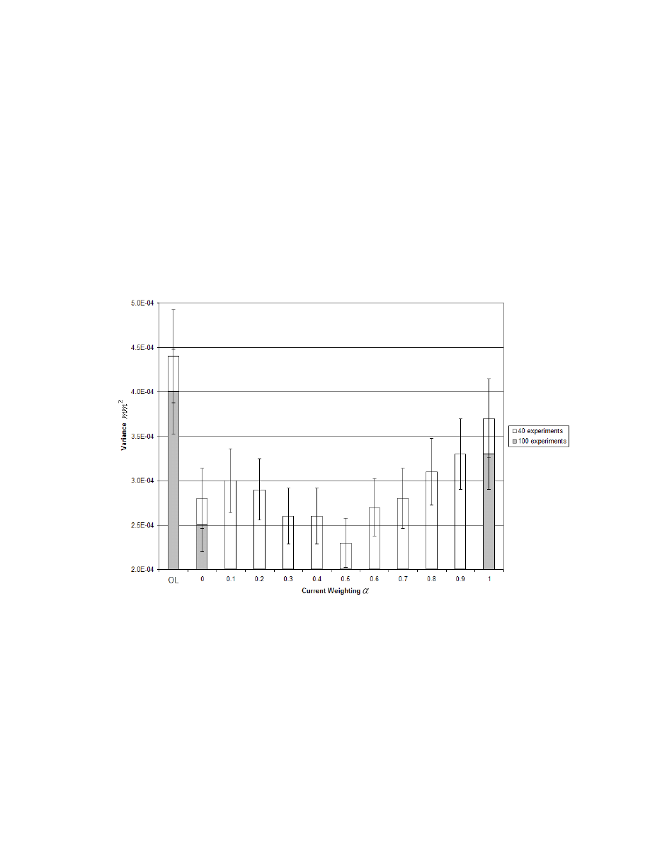
89
5.1.2.4
Variance Calculation for Each α Value
In order to determine the best α value that will give the most consistence welds, the
variance for the mean nugget diameter for each α has been similarly calculated as in
Chapter 4, equation (4.5). The results for each α value as well as the results that have
been previously calculated for open voltage, constant current, and constant voltage
control modes are shown in Figure
5-5, where OL stands for Open Voltage Control mode
(Open-Loop). 40 experiments were done first for each of the three control modes, open
voltage, constant current and constant tip voltage and their variances were compared to
the variance calculations for the other alpha values.
Figure
5-5: Variance comparison in nugget diameter using tip voltage
It is obvious that increasing α initially decreases the variance of the nugget size,
and then increases the variance. When α = 0.5, the variance of the nugget size is the
smallest, and with this control index, approximate 33% improvement in variance in weld
nugget diameter versus constant current control (α = 1) and 18% improvement versus
constant voltage control (α = 0) is achieved. The analysis results indicate that 50%

90
weighting on the weld current or 50% weighting on the tip voltage produces the most
consistent weld nugget diameter.
Then 60 more experiments were done for each of the open loop voltage, constant
current and constant tip voltage control mode, to ensure the accuracy of our results after
doing 100 experiments in total for each of the three control modes. We noticed almost
9% improvement shown in each of the three control modes variance calculations, which
could be due to improving the power cables for the power supply to increase it is
efficiency before performing the 60 more experiments.
Comparing the new results for the three control modes to the other alpha values,
we get, when α = 0.5, the variance nugget size is still the smallest and with this control
index, approximate 30% improvement in variance in weld nugget diameter versus
constant current control (α = 1) and 9% improvement versus constant voltage control (α =
0) is achieved. The analysis results indicate again that 50% weighting on the weld
current or 50% weighting on the tip voltage produces the most consistent weld nugget
diameter. Therefore, we can conclude that, when the controller under the constant power
control mode, we get the most consistency in the spot weld nugget diameter.
Moreover, since 100 experiments were done for each of the open loop voltage
control, constant current control and tip voltage control, and only 40 experiments were
done for the other alpha values from 0.1 to 0.9, a moving average was calculated for
these alphas. Figure
5-6 shows the plot for the moving average calculated for the
variance for each of the other alphas from 0.1 to 0.9 compared to the 100 experiments
results for each of the three control modes, open loop voltage, constant current, and
constant tip voltage.
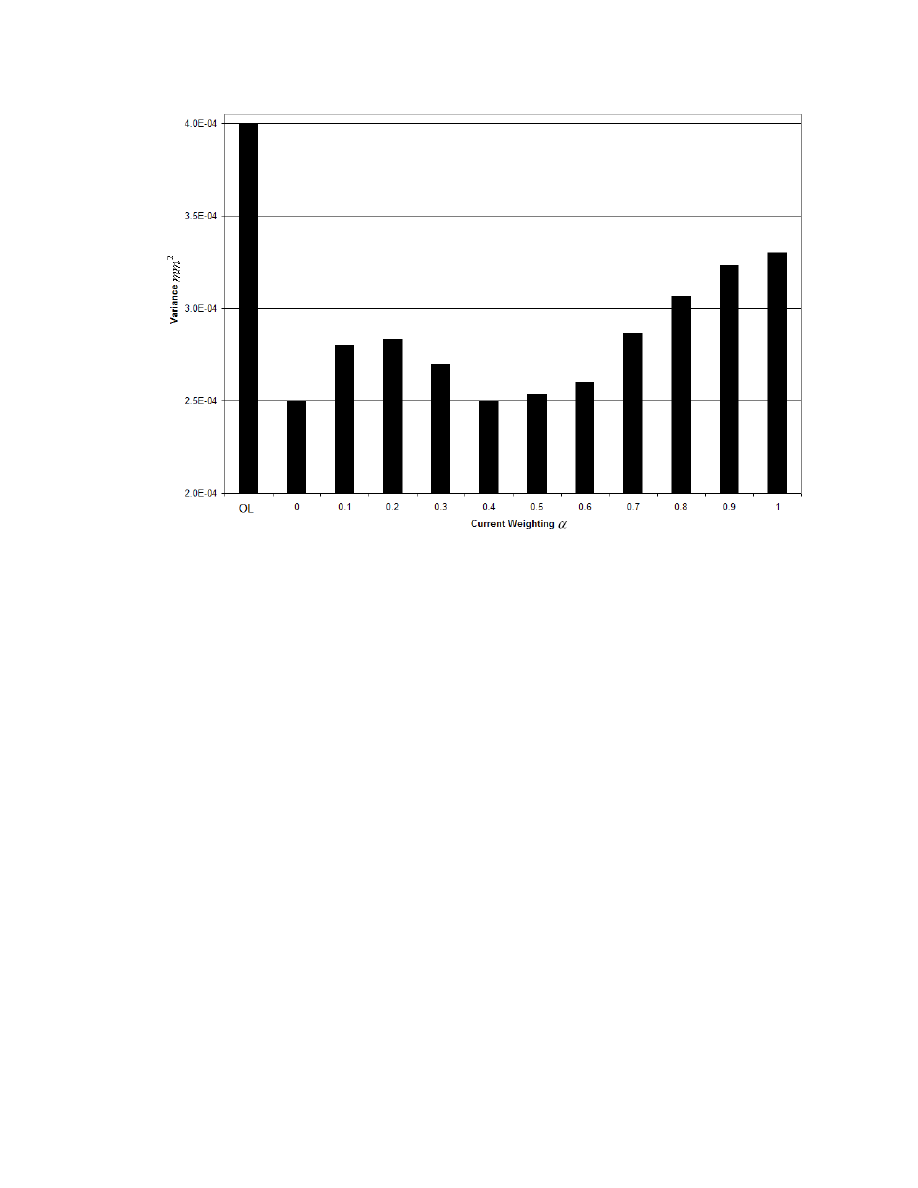
91
Figure
5-6: Variance comparison in nugget diameter using tip voltage moving
average
5.2
Generic Power Control Mode Using Nominal
Voltage with Weld Current
This section will repeat section
5.1 control strategy, with using nominal voltage as a
feedback with the weld current instead of the tip voltage, to be able to see how much
improvement our controller achieved in reducing the variance for the nugget diameters
for each alpha value compared to Jing Bai’s controller, since for that work only nominal
voltage was used.
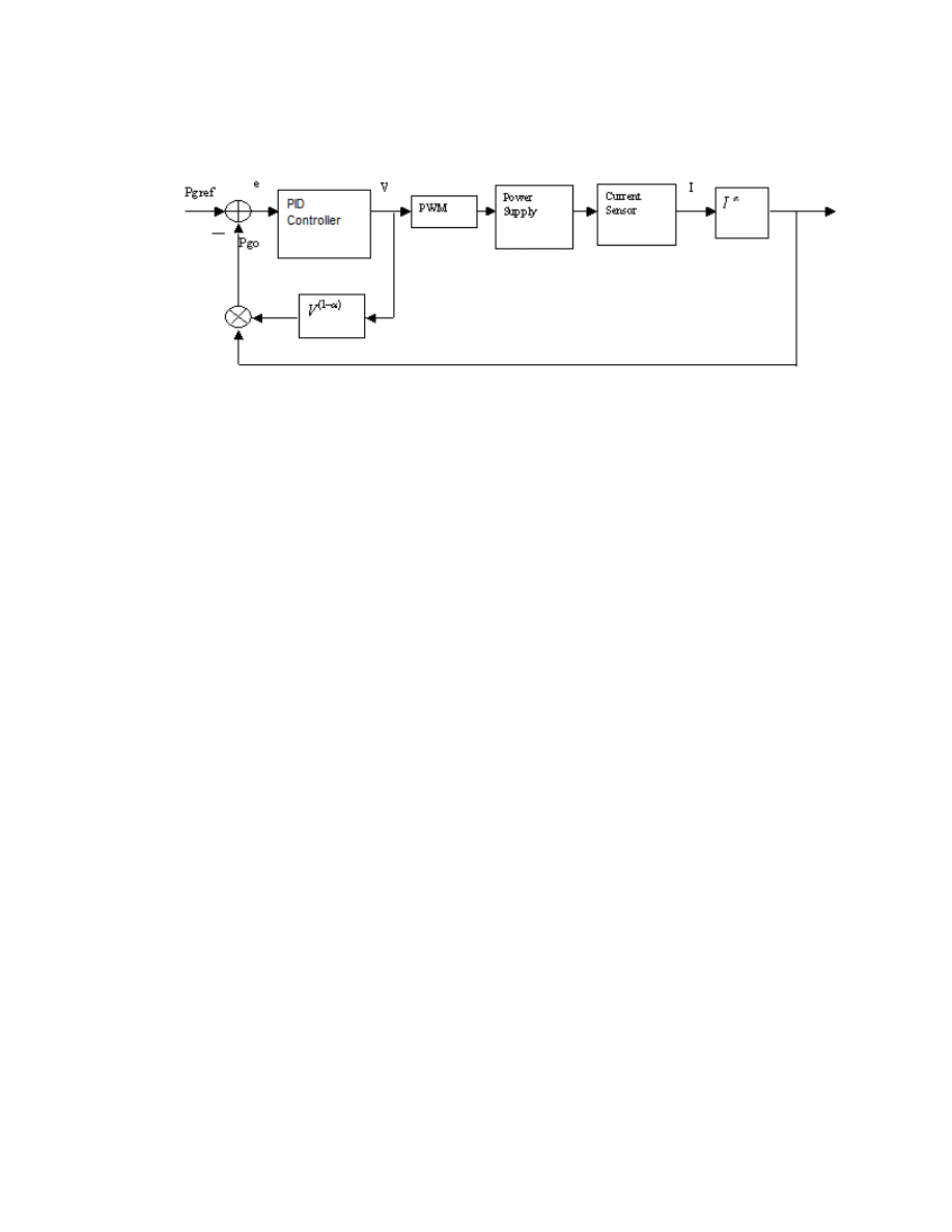
92
5.2.1
Control Strategy Design
Figure
5-7: Nominal voltage generic power control mode
Figure
5-1 has been modified to Figure
5-7, using the nominal voltage as a feedback to
the PID control, which uses the same generic control mode equation as equation(5.3).
5.2.2
Application of Strategy to Welding 0.152mm Gauge
Stainless Steel
Similar to section
5.1, a series of welds were conducted and the variance of the nugget
diameter was measured for the 11 values of α from 0 to 1 by 0.1 increments. Then the
mean nugget diameter as well as the variance for each α has been calculated to determine
the best α value that will give the most consistent spot welds.
5.2.2.1
Determining Set Point for Each α
For calculating the set point for each of the different α values, the set points for the
constant current control mode (α=1) and the open voltage control mode (α=0) are used in
the following expression:
(1
)
(42.5)
(316)
Pgo
α
α
−
=
×
(5.5)
Where 42.5% is the duty cycle that was chosen as one of the operating points for
performing the open voltage control mode. In this control mode the duty cycle becomes
as a measurement of the open circuit voltage, and we are operating at this measurement
of voltage.

93
Table
5-5 lists the calculated set points for each α value.
Table
5-5: Set points at different α values
α
Set Points Pgo
α
Set Points Pgo
0.0
42.500
0.6
141.634
0.1
51.942
0.7
173.100
0.2
63.482
0.8
211.557
0.3
77.585
0.9
258.558
0.4
94.822
1.0
316.000
0.5
115.888
5.2.2.2
PID Controller Gains Tuning for Each α
Table
5-6
lists the tuned PID controller gains for each of the set points (Table
5-5)
calculated for each α value using Ziegler Nicholas tuning method as described earlier.
Table
5-6: PID controller gains values for different α values
α
Set Point
Kp
Ki
Kd
0.1
51.9
0.0125
75
7.633 x 10
-6
0.2
63.5
0.0250
150
1.527 x 10
-5
0.3
77.6
0.0375
225
2.290 x 10
-5

94
0.4
94.8
0.0500
300
3.053 x 10
-5
0.5
116
0.0625
375
3.816 x 10
-5
0.6
142
0.0750
450
4.580 x 10
-5
0.7
173
0.0875
525
5.343 x 10
-5
0.8
212
0.1000
600
6.106 x 10
-5
0.9
259
0.1125
675
6.869 x 10
-5
5.2.2.3
Performing Series of Welds for Each α
Similar to section
5.1, 40 welds were done for each α value to measure the mean nugget
diameter for each, to ensure that the set point calculated for each gave the same or close
mean nugget diameter as the constant current control and the open voltage control mode.
Table
5-7 lists the mean nugget diameters for each α value.
Table
5-7: Mean nugget diameter for each α’s set point
α
Set point
Mean nugget diameter (mm)
0
42.500
0.30235
0.1
51.942
0.30017
0.2
63.482
0.30103
0.3
77.585
0.30050
0.4
94.822
0.30345

95
0.5
115.888
0.30097
0.6
141.634
0.30110
0.7
173.100
0.30450
0.8
211.557
0.30033
0.9
258.558
0.30048
1
316.000
0.3005
5.2.2.4
Variance Calculations for Each α Value
Figure
5-8 shows the variance for the mean nugget diameter for the different α values.
The results for using the nominal voltage as a feedback with the weld current, are
showing that the smaller the α values the higher the variance than the results for using the
tip voltage as a feedback with the weld current. While as the α value increases, the
variance for the mean nugget diameters for using the nominal voltage, is similar or close
to the variance for the mean nugget diameters for using the tip voltage with the weld
current, due to the less impact of the voltage in the controller behavior as the α values get
closer to 1.
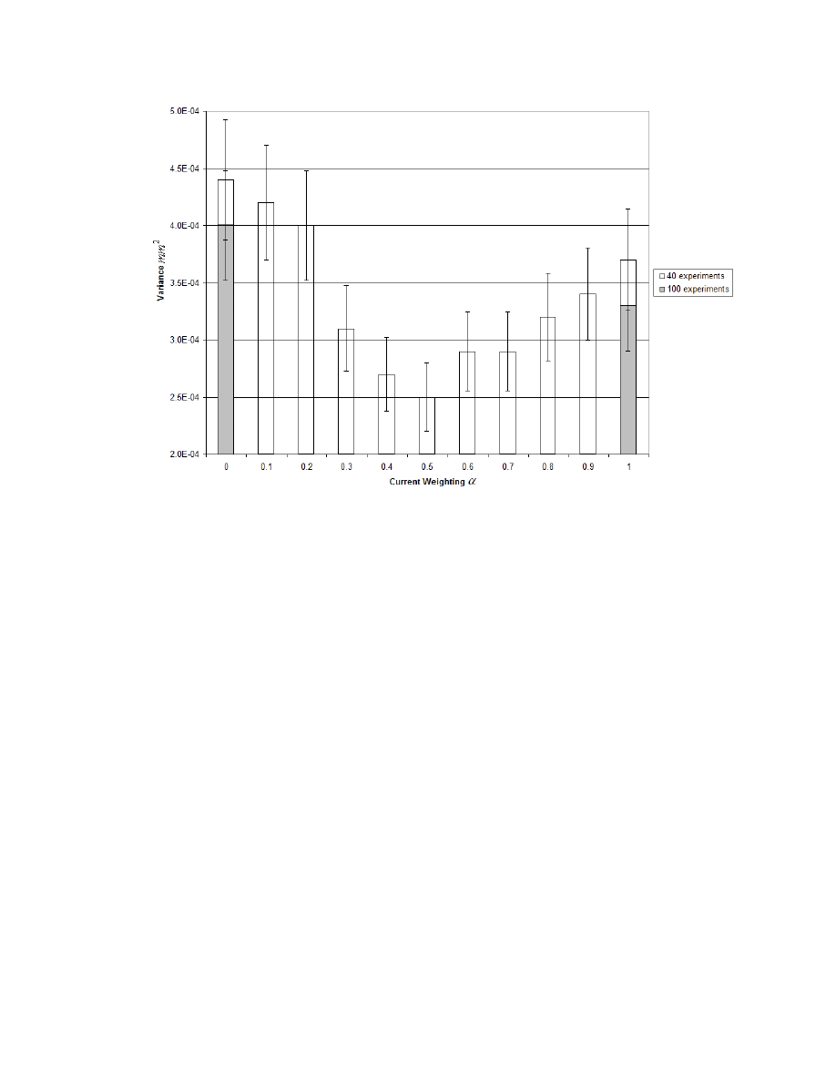
96
Figure
5-8; Variance comparison in nugget diameter using nominal voltage
Similar to section 5.1.2.4, the 40 experiments for each of the open loop voltage &
constant current control modes were compared first to the variance calculations for the
other alpha values. The variance calculation for using the nominal voltage gave the same
results as the variance calculation for using the tip voltage. When α = 0.5, the variance of
the nugget size is the smallest. With this control index, approximate 32% improvement
in variance in weld nugget diameter versus constant current control (α = 1) is achieved
and 43% improvement versus the open loop voltage control (α = 0) is achieved. The
analysis results indicate that 50% weighting on the weld current or 50% weighting on the
nominal voltage produces the most consistent weld nugget diameter.
Comparing the new results for each of the open loop voltage and constant current
control modes after doing more 60 experiments for each, with the variance calculation for
the other alpha values. The results indicated that, when α = 0.5, the variance nugget size
is still the smallest, with this control index, approximate 24% improvement in variance in
weld nugget diameter versus constant current control (α = 1) is achieved and 37.5%
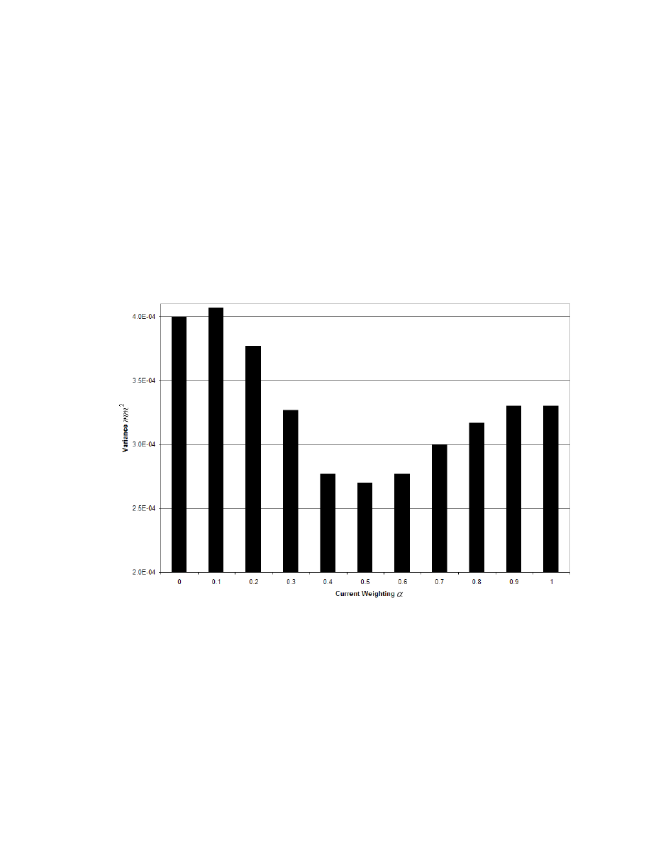
97
improvement versus open loop voltage control (α = 0) is achieved. The analysis results
indicate again that 50% weighting on the weld current or 50% weighting on the nominal
voltage produces the most consistent weld nugget diameter. Therefore, when the
controller under the constant power control mode, we get the most consistency in the spot
weld nugget diameter.
Similar to the tip voltage results, a moving average was calculated for the alpha values
from 0.1 to 0.9 as shown in Figure
5-9, since only 40 experiments were done for these
alpha values and 100 experiments were done for each of the open loop voltage and
constant current control modes.
Figure
5-9: Variance comparison in nugget diameter using nominal voltage moving
average
5.3
Control Variable Variance
In order to know if the improvement in variance of the weld nugget diameters for the
different α values, is a result of a better controller implementation or not, the variance of

98
the control variables was calculated. The variance of the controlled variable is defined
as:
20
(1
)
2
1
0
2
2
1
1
(
( )
( )
( ))
20
( )
n
i
i
i
t
c
V
t I
t
P
n
P
α
α
α
σ
α
−
=
=
−
=
∑
∑
(5.6)
where, n is the number for welds for each α value (which is 40 welds), t is the weld time,
(1
)
( )
( )
i
i
V
t I
t
α
α
−
is the product of the voltage and current of the control variable of the
nugget sample i at different α values, ( )
P
α
is the desired power set point, and
2
c
σ
is the
variance.
For the open loop voltage control mode, the output voltage (duty cycle) was
controlled directly; the PID controller was not used, therefore the variance in the control
variable was not calculate for this mode. Figure
5-10 shows the variances of control
variables over the whole welding process under each of the closed loop power control
modes using the tip voltage as feedback with the weld current, where α=0 in the graph
represents the constant tip voltage control mode. It is indicated that the variance is the
smallest when α is set to 0.1, while when α is equal to 0.5, the variance is the highest.
The analysis shows that the improvement of welding consistency seen, with the optimal
control strategy is not a result of better controller implementation at alpha values near
0.5.
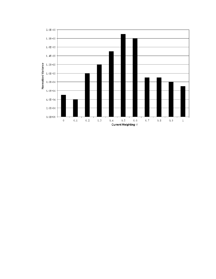
99
Figure
5-10: Normalized variance comparison in control variables for each α value
using tip voltage
Figure
5-11 shows the variances of control variables over the whole welding
process under each of the closed loop power control modes using the nominal voltage as
a feedback with the weld current, where α=0 is not shown in the graph because in this
case it represents the open loop voltage control, which is independent of the PID
controller. The results is slightly different, but it is similar to the results of the variance
of the control variables using the tip voltage, where it is the smallest when α is set to 0.1,
while when α is equal to 0.5, the variance is the highest. The analysis shows again that
the improvement of welding consistency seen; with the optimal control strategy is not a
result of better controller implementation at that point.
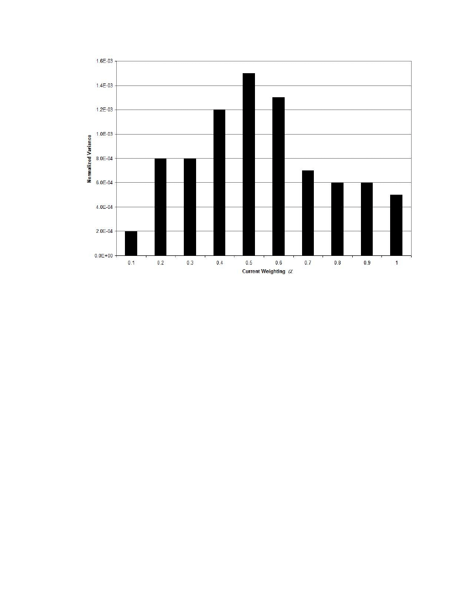
100
Figure
5-11: Normalized variance comparison in control variables for each α value
using nominal voltage
5.4
Summary of the Experiments
1)
Ramp test for open loop voltage control mode have been performed firstly to
determine adequate variables and best operating point ensuring the welding quality:
a)
Duty Cycle of the PWM: 42.5%
b)
Welding time: 20ms
c)
Weld force: 4lb
2)
After doing hundred welds at this set point, the mean nugget size was achieved.
Meanwhile the output currents and tip voltages were obtained from the sensing
circuits. Then the mean current and mean voltage were determined as 315A and
1.035V respectively. So the initial estimates of the set points were then evaluated as:

101
(1
)
(1.035)
(315)
Pgo
α
α
−
=
×
for the using the tip voltage as a feedback with the weld
current for the PID controller.
3)
Under the pure current (Pg = 315) & voltage control (Pg = 1.035) modes, a PID
controller was tuned using Ziegler Nichols method to get between 5.1% & 10.9%
overshoots respectively with fastest rise time.
4)
100 welds were then done for each of the pure current control mode and voltage
control mode to find the mean current and mean voltage that will achieve the same
mean nugget diameter as the open voltage control mode. As a result the set points for
current control mode and voltage control mode that produced identical nugget
diameter were 316A & 1.036V.
5)
The set points for the remaining α were then evaluated as
(1
)
(1.036)
(316)
Pgo
α
α
−
=
×
for using the tip voltage feedback with the generic power control mode, while it was
evaluated as
(1
)
(42.5)
(316)
Pgo
α
α
−
=
×
for using the nominal voltage feedback with
the generic power control mode.
6)
At each of the set points for both cases (tip voltage or nominal voltage feedbacks), the
PID controller was tuned to get 5%−11% overshoot with maximizing the speed of
response. A series of experiments were conducted around these operating points to
experimentally determine the set point that produced the same nugget size as used for
the open loop voltage control, constant current control and constant voltage control.
Then 40 welds were done at each of the identified set points, which were used to
measure weld nugget size. The means and variances were then calculated.
7)
Variance of nugget diameter for evaluating weld quality has been studied.
8)
Analysis of the variance of nugget size indicated that among the different control
variable for the generic power control mode under study, the best welding quality was
achieved when α = 0.5, which is the constant power control mode.

102
9)
For comparing the closed loop power controllers, analysis of the variance of control
variable concluded that the proceeding result was not a result of the quality of the
controller design.

103
Chapter 6
6
Conclusion and Future Work
6.1
Summary of Achievements
Based on the detailed discussion on experimental design and data analysis results, the
main achievements of this thesis are:
• A new power supply strategy to improve the consistency of resistance spot
welding for every spot weld was investigated. And a generic power control mode
has been discussed and implemented for the resistance spot welding process. The
three control modes, voltage control, current control and power control modes can
be seen as three special points of this generic power control mode.
• Novel DC power supply for small scale RSW in this study was modified and
described. A Hall effect current sensor and a tip voltage sensor were built, so that
the load current and tip voltage analog signals were measured to support
implementing the control schemes. The power supply is a pulse width modulated
DC-DC converter. Thus its nominal output is given by the duty cycle times the
maximum voltage of 13.5V.
• The modification that was done for the novel DC power supply was in the
controller section by replacing the 8-bit microcontroller, PIC 16F73 from
Microchip, Inc. with the option of using an externally supplied pulse width
modulated (PWM) signal, or generating its own PWM signal from an analog
PWM chip. The set point for the analog PWM chip can be generated internally as
a fixed value, from a built-in analog PID controller or from an external analog
signal. Normally we generate the external PWM signal from a DSPACE control
board (DSP) with a controller implemented with Open Desk software. In total
there are 5 operating modes:
o
External PWM signal

104
o
External analog reference for the PID controller
o
External analog duty cycle (D)
o
Internally generated duty cycle (D)
o
Internally generated reference with PID controller
• Both the built-in controller and the controller implemented on the control board
have the option of using tip voltage or welding current as feedback variables.
• Three DC power supply units were built after the modification, where each can
give up to 1000A.
• An experimental approach for finding the optimum control variable for resistance
spot welding was investigated. For 0.152mm thick stainless steel coupons, the
weld quality under different control variables has been analyzed based on the
experimental data. The results demonstrated that a 50% weighting on the voltage
produced the most consistent welds. With this control variable, substantial
improvement in variance in nugget size compared with constant current control
and was achieved.
• The stability of the different closed loop power control modes has been analyzed
based on the experimental data. The results indicated that the control scheme with
α
= 0.5 is the most stable one among the control modes under study.
6.2
Future Work
Based on the achievements of this thesis, the following tasks are recommended for
further research and study:
• Repeat this research approach to not only achieve consistent welds, but to also
achieve stronger welds.

105
• The new power supply control strategy can be applied for other specific weld
geometry, and the potential for this approach for different weld materials can be
compared.
• Connecting the three power supply units that were built after the modification in
parallel, and repeat this research using the three connected units with thicker
materials.
• Build three more power supply units and connect in parallel with the already built
ones using two 12V batteries to achieve 6000A power supply to move form
SSRSW to LSRSW to help improve the automotive industry RSW process.
• Repeat this research with the six units to improve the consistency of the spot-
welds for the LSRSW.
6.3
Conclusion
In literature lots of work has been done in improving the control scheme and the power
supply for RSW since the 1940s till now, and there is still more to do to improve it. This
research work was done to help in the improving process for RSW, and still more to be
added to it, as shown in the future work section.
During the process of modifying the RSW power supply and building new units, I
was able to gain new experience and learn new information in power electronics area,
working with hardware, designing circuit boards, working with different electronic chips,
etc. I was also able to learn new software skills, by working with new design softwares,
such as Solid Works, CirCAD, and Eagle software to design the new power supply unit.
More than half of my research work was practical than theory, which was a great
chance for me to learn hands on experience in the electrical engineering control field,
than just applying theory and math without seeing the practical side of it, that in some
cases doesn’t fully agree with the theory and math. I am so grateful to my Ph.D.
supervisor for giving me this chance that will help me for sure in the future, once I obtain

106
a teaching position, to teach my students the practical experience I gained along with the
theory, for them to get a better understanding of the electrical engineering field.
As a result of this research work, a simple designed, fully independent, portable,
and inexpensive RSW power supply was built. Constant tip voltage feedback was
implemented with the PID controller designed to control our RSW power supply, which
gave a smaller nugget diameter variance compared to Open loop voltage control and
constant current control modes.
A constant tip voltage controller provided the most consistent welds when
compared to constant current and open loop voltage control. Specifically we saw a 24%
reduction in the variance as compared to constant current control. This control approach
allows for automatic adjustment of the power supplied for variations in the contact area,
eliminating the need for setting a setpoint schedule. However while performing these
experiments we found one serious drawback with the constant tip voltage control
approach. In the case where expulsion occurs, the power supply responds very poorly.
With expulsion and the associated loss of metal, there is step drop in the weld
resistance and thus a corresponding drop in the tip voltage. The welder responds by
increasing the duty cycle and increasing the energy supplied to the weld. As expulsion is
typically associated with excess energy to the weld, this is an undesirable response. Thus
constant tip voltage should be implemented in combination with an expulsion detection
algorithm that either terminates the weld or reduces the setpoint in response to
expulsions.
We extended this result by considering the use of a weighted average of current
and voltage as the feedback variable and to see how much improvement in the
consistency of the weld process we will get. This research work compared to Jing Bai’s
research work
[18] showed improvement in the mean nugget diameter variance. The
variance calculations for using both tip voltage and nominal voltage, were smaller for all
the α values than the variance calculated in Jing Bai’s research using only the nominal
voltage.

107
Finally, this research resulted in a good starting operating point in improving the
consistency for RSW that with more research work could give more improvement. That
concludes that the RSW research will keep going on for the perfect RSW control and
power supply that once a button is pushed, a perfect spot weld is made.

108
References
[1]
B. H. Chang, M. V. Li, and Y. Zhou, A comparative study of ’small-scale’ and
’large scale’ resistance spot-welding
, Science and Technology of Welding and Joining,
vol. 6, pp. 273–280, 2001.
[2]
A. G. Livshits, Universal quality assurance method for resistance spot welding
based on dynamic resistance
, Welding Journal, vol. 76, 1997.
[3]
R. T. Wood, L. W. Bedard, J. F. Bedard, B. M. Bernstein, J. Czechowski, M. M.
D’ndrea, and R. A. Hogle, A closed-loop control system for three-phase resistance spot
welding
, Welding Journal, vol. 64, 1985.
[4]
K.J. Ely and Y. Zhou. Microresistance spot welding of Kovar, steel, and nickel.
Science and Technology of Welding and Joining, Vol.6, No.2, PP 63-72, 2001.
[5]
D. Steinmeier. Downsizing in the world of resistance welding. Welding Journal,
Vol. 77, PP39-47, July 1998.
[6]
L. J. Brown, and J. Lin, Power Supply Designed for Small-Scale Resistance Spot
Welding
, American Welding Society, Dallas, Tex., April 25-28, 2005.
[7]
L. J. Brown, Power Supply and Control Equipment for a Resistance Welding
Machine
, U.S. Patent #6,825,435, Nov. 30, 2004.
[8]
Jun Lin, Power Supply Designed for Small-Scale Resistance Spot Welding,
Thesis; ECE Department; UWO; 2005.
[9]
N. T. Williams, Use of voltage integration for monitoring and feedback,
Resistance Welding Control and Monitoring, TWI, 1977.
[10]
J. Heb, T. Kem, W. Krigl, and M. Schweizer, Visualization of the resistance spot
welding process in the production line
, Welding Journal (Miami, FL, U. S.), vol. 77(12),
pp. 495–502, 1998.
[11]
S. R. Patange, T. Anjaneyulu, and G. P. Reddy, Microprocessor-based resistance
spot welding monitor
, Welding Journal, vol. 64, pp. 33–38, 1985.

109
[12]
D. W. Steimier, Downsizing in the world of resistance spot welding, Welding
Journal, vol. 77, pp. 39–47, 1998.
[13]
D. Dickinson, Welding in the automotive industry, Technical Report, a review
report on AISI Project 1201-409C, American Iron and Steel Institute, 1981.
[14]
L. J. Brown and J. Lin, Power supply designed for small-scale resistance spot
welding
, Welding Journal, 2005.
[15]
G. R. Archer, A new system for automatic feedback control of resistance spot
welding
, The International Journal of Advanced Manufacturing Technology, vol. 38, pp.
987–993, Oct. 1959.
[16]
W. L. Roberts, Resistance variations during spot welding, Welding Journal, vol.
30, pp. 1004–1019, Nov 1951.
[17]
J. S. Moon, G. S. Kim, J. M. Kim, and C. Y. Won, Power control of resistance
spot welding system with high dynamic performance
, Industrial Electronics, Control and
Instrumentation. IECON 97. 23rd International Conference, vol. 2, pp. 845–849, 1997.
[18]
Jing Bai, Improved Consistency of Resistance Spot Welding via Power Supply
Control Strategy
, Master’s thesis, ECE Department, UWO, 2008.
[19]
S. Duisburg, The welding engineers current knowledge, Book, Edition 2008.
[20]
N. T. Willian, Welding, brazing and soldering , ASM Handbook, vol. 6, 1993.
[21]
W. Li, S. J. H, and J. Ni, On-line quality estimation in resistance spot welding,
Journal of Manufacturing Science and Engineering, Transaction of the ASME, Vol. 122,
2000.
[22]
Y. Zhou, S. J. Dong, and K. J. Ely, Weldability of thin sheets metals by small-
scale resistance spot welding using high-frequency inverter and capacitor-discharge
power supply
, Journal of Electrical Materials, vol. 30, 2001.

110
[23]
D. W. Dickinson, J. E. Franklin, and A. Stanya, Characterization of spot welding
behavior by dynamic electrical parameter monitoring
, Welding Journal, vol.59, pp. 170–
176, 1980.
[24]
K. Ely and Y. Zhou, Microresistance spot welding of Kovar, steel, and nickel,
Science and Technology of Welding and Joining, vol. 6, pp. 63–72, 2001.
[25]
X. T. Zhang, Operating condition identification and electrode condition
monitoring in resistance spot welding process
, Master’s thesis, The University of
Western Ontario, London, ON, Canada, 2002.
[26]
J. E. Gould, Welding research supplement, Welding Journal, vol. 66, pp. 1–10,
1987.
[27]
J. G. Kaiser, G. L. Dunn, and T. W. Eagar, Welding research supplement, Journal
of Electrical Materials, vol. 61, pp. 167–174, 198
2.
[28]
D. W. Dickson, J. E. Franklin, and A. Stanya, Welding research supplement,
Journal of Electrical Materials, vol. 59, pp. 170–196, 1980.
[29]
Y. Zhou, P. Gorman, W. Tan, and K. J. Ely, Weldability of thin sheet metals
during small-scale resistance spot welding using an alternating-current power supply
,
Journal of Electrical Materials, vol. 29, pp. 1090–1099, 2000.
[30]
A. V. Demnsion, D. J. Toncich, and S. Masood, Control and process-based
optimisation of spot-welding in manufacturing systems
, The International Journal of
Advanced Manufacturing Technology, Vol. 13, p. 256, 1997.
[31]
J. Senkara, H. Zhang, and H. S. J, Expulsion prediction in resistance spot
welding
, Welding Journal, vol. 83, p. 123, 2004.
[32]
H. Zhang and J. Senkara, Resistance Welding: Fundamentals and Applications,
CRC Press, Taylor & Francis Group, 2006.
[33]
S. Nakata, S. Aono, M. Suzuki, Y. Kawaguchi, and M. Inoue, Quality assurance
characteristics in resistance spot welds by adaptive control system and its field
applications
, presented at Annual Assembly of IIW, 1982.

111
[34]
N. Malbotra, Online tip voltage and resistance measurement in RSW process,
Master’s thesis, The University of Western Ontario, London, ON, Canada, 2005.
[35]
L. J. Brown and Y. J. Sun, Tuning to Stabilize Adaptive Internal Model Controller
for Periodic Disturbance Cancellation
, IEEE Conference on Decision and Control, San
Diego, CA, USA, P. 1914, 2007.
[36]
J Z Chen and D F Farson, Electrode Displacement Measurement Dynamics in
Monitoring of Small Scale Resistance Spot Welding
, Institute of Physics publishing,
Measurement Science and Technology, 2419-2425, 2004.
[37]
Hua Wang, Yansong Zhang, and Guanlong Chen, Resistance Spot Welding
Processing Monitoring based on Electrode Displacement Curve using Moving Range
Chart
, Journal, Measurement, 1032-1038, 2009.
[38]
Ivan Polajnar, Janez Grum, Elsayed A. Esmail, Sources of Acoustic Emission in
Resistance Spot Welding
, Česká společnost pro nedestruktivní zkoušení materiálu 38.
mezinárodní konference Defektoskopie 2008 Brno, 4. – 6. 11. 2008.
[39]
L. J. Brown and J. S. Schwaber, Identifying operations from pre-weld information
for resistance spot welding
, Proceedings of the American Conference, Vol. 3, p. 1535,
2000.
[40]
D. F. Farson, J. Z. Chen, K. Ely, and T. Frech, Monitoring resistance spot nugget
size by electrode displacement
, Journal of Manufacturing Science and Engineering, Vol.
126, p. 391, 2004.
[41]
Yujuan Sun, Instantaneous Fourier Series Estimation, Thesis, Yujuan Sun, ECE
department, UWO, 2006.
[42]
Jin Lin, Power Supply designed for Small Scale Resistance Spot Welding, Thesis,
ECE department, UWO, 2005.
[43]
L. J. Brown and J. Lin, Power Supply Designed for Small-Scale Resistance Spot
Welding
,
Welding Journal, p 25-28, April 2005.

112
[44]
L. J. Brown and J. Bai, Improved Consistency for Resistance Spot Welding via
Power Supply Control Strategy
, Material Science and Technology conference
(MS&T’08) 2008.
[45]
Daniel W. Hart, Introduction to Power Electronics, by Prentice Hall Inc., ISBN
0-02-351182-6, PP 193, 1997.
[46]
K. I. Johnson, Resistance Welding Quality-control Techniques, Metal
Construction and British Welding Journal, Vol. 5, p 176-181, May 1983.
[47]
H. Zhang, J. Senkara, RESISTANCE WELDING: Fundamentals and Applications,
CRC Press, Taylor and Francis Group, 2006
[48]
E. W. Kim and T. W. Eagar, Parametric Analysis of Resistance Spot Welding
Lobe Curve
, International Congress and Exposition, Detroit, Michigan, 1988
[49]
N. S. Nise, Control Systems Engineering, Fourth Edition, John Wiley & Sons.
Inc, 2004.
[50]
T. Jansen, J. Eggers, and R. Bothfeld, GeniusMFI IQR – a New Inverter Power
Supply with Adaptive Regulation System to Assure the Quality for Resistance Spot
Welding
, The 5
th
International Seminar on Advances in Resistance Welding, Toronto,
Canada, 24-26 September 2008.
[51]
F. G. B. C. Kuo, Automatic Control System, P. in the United States of America,
Ed. Copyright John Wiley and Sons Inc, 2003.
[52]
M. Araki, PID Controller, Control Systems, Robotics, and Automation – Vol. II,
2000.
[53]
J. Zhong, PID Controller Tuning – A Short Tutorial, Mechanical Engineering,
Purdue University, Spring 2006
[54]
Wikipedia, 555 Timer IC (
http://en.wikipedia.org/wiki/555_timer_IC
)
[55]
Brain R. Copeland, The Design of PID Controller Using Ziegler-Nichols Tuning,
March 2008.

113
[56]
American Welding Society, Miami, FL. Welding Handbook, eighth edition, 1991.
[57]
American Welding Society, Miami, FL. Recommended Practices for Resistance
Welding,
1966.
[58]
Unitek PECO technique support manual, Fundamentals of small parts resistance
welding
, Sept. 2002.
[59]
David Steinmeier, Resistance Welding – Trouble Shooting Guide, microJoining
Solutions – microTips
TM
, Arcadia, California, 2006.
[60]
David Steinmeier, Resistance Welding – Power Supply Feedback Mode Selection,
microJoining Solutions – microTips
TM
, Arcadia, California, 2007.
[61]
W. Pei, Z. Wenqi, Measurement of Dynamic Resistance in Resistance Spot
Welding
, Institut for Produktion og Ledelse, DTU, 2005.
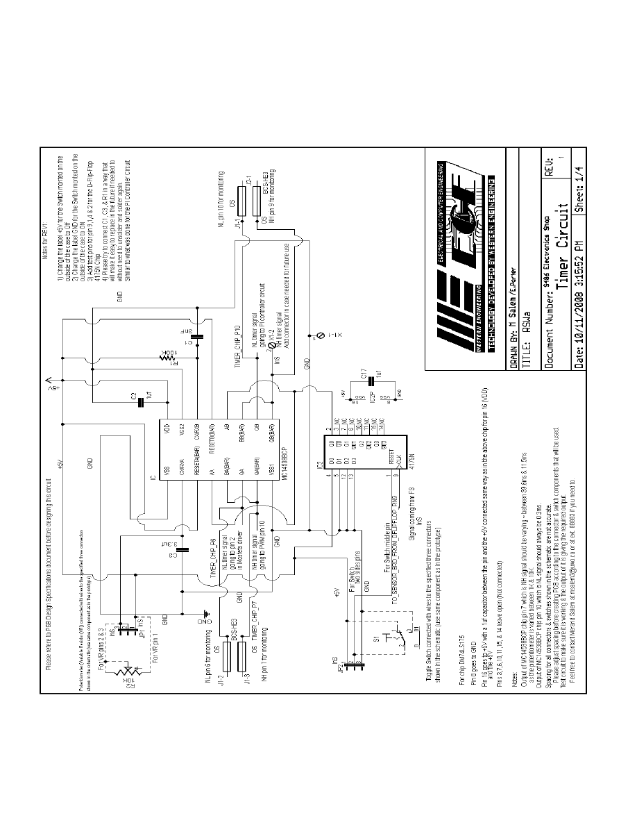
114
Appendix A
RSW Power Supply Circuit Schematics
Figure A- 1: Timer circuit schematic
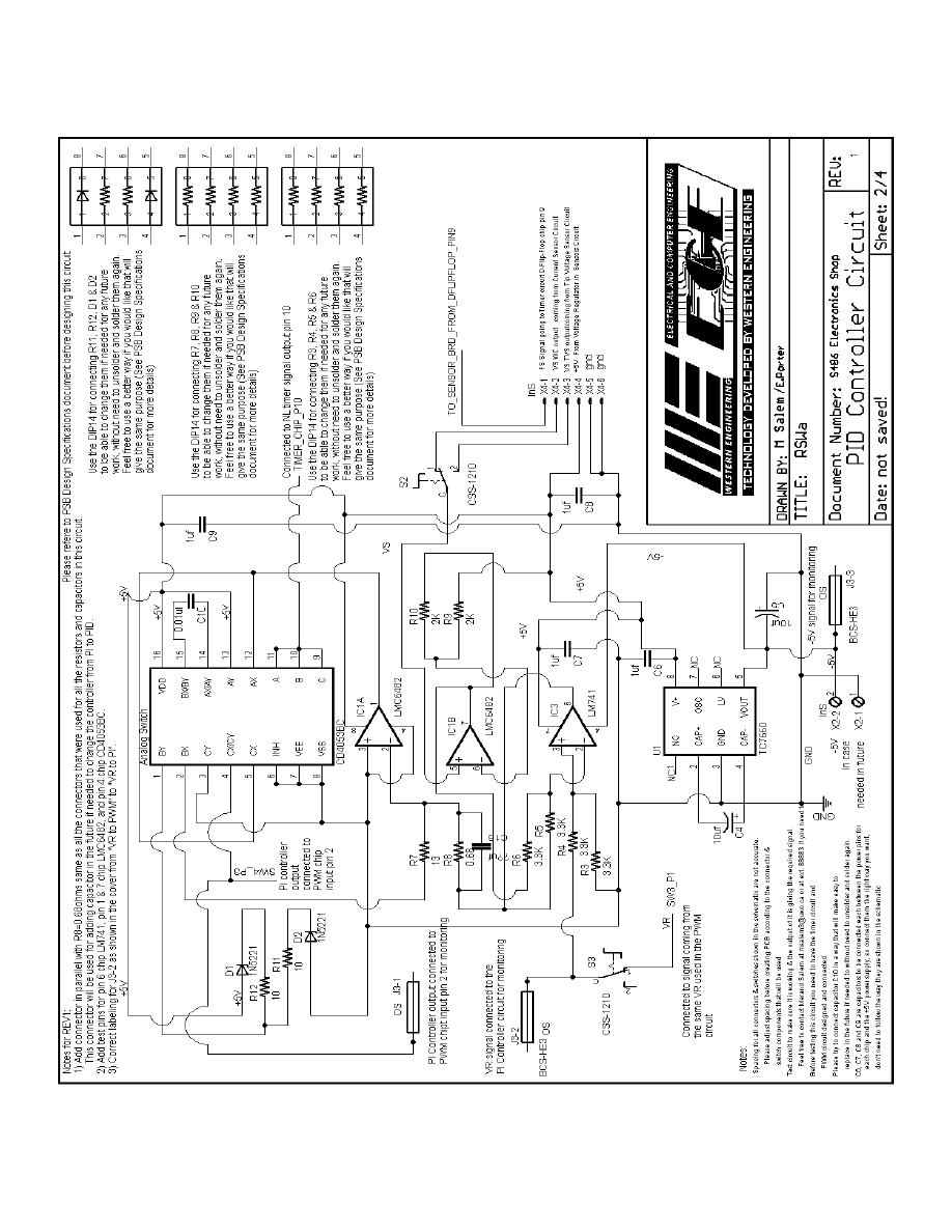
115
Figure A- 2: PID circuit schematic
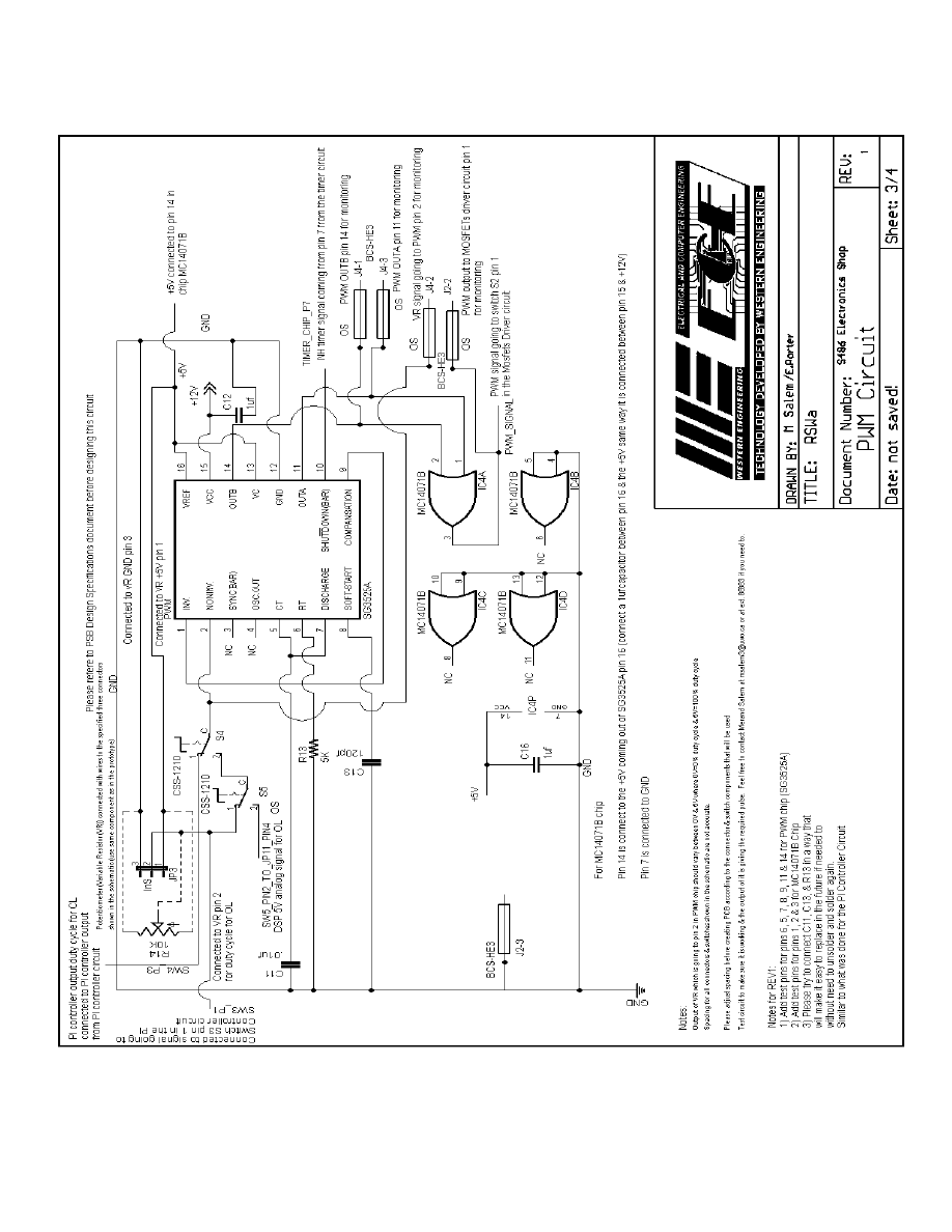
116
Figure A- 3: PWM circuit schematic
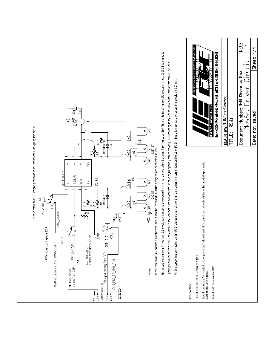
117
Figure A- 4: MOSFETs driver circuit schematic
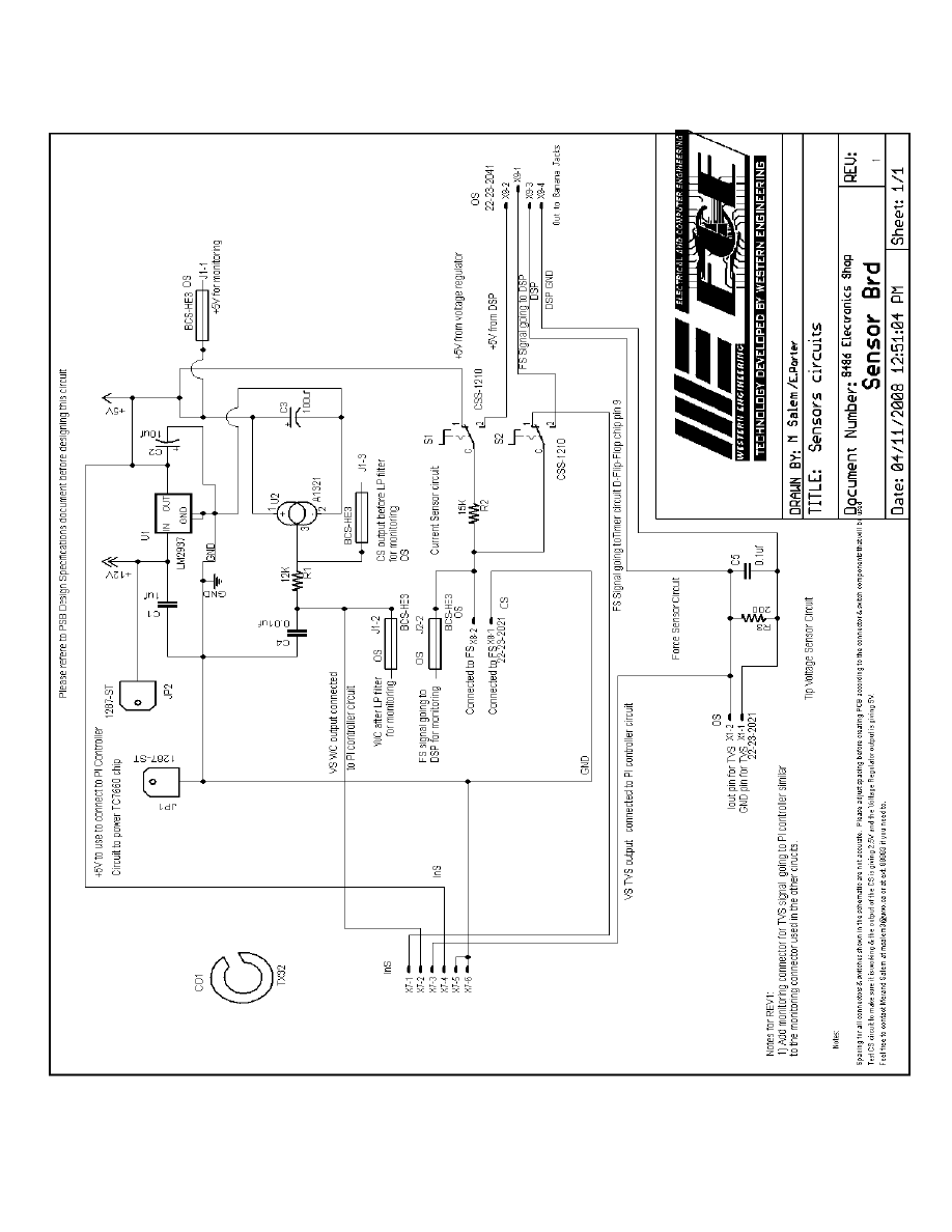
118
Figure A- 5: Sensors circuit schematic
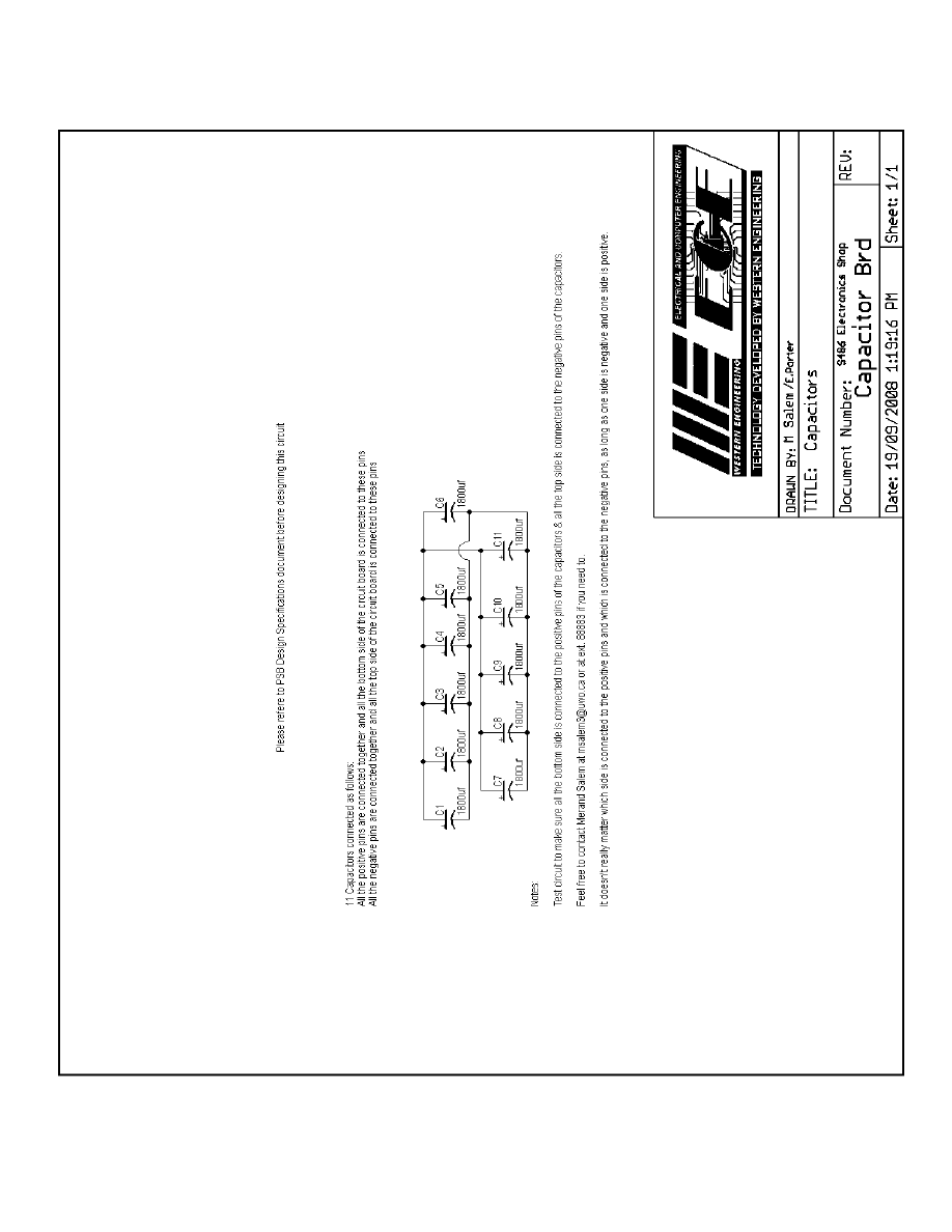
119
Figure A- 6: Capacitor circuit schematic
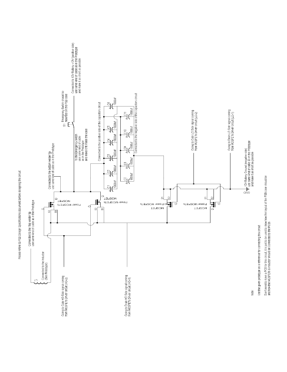
120
Figure A- 7: Power supply power components circuit schematic

121
Curriculum Vitae
Name:
Meranda Salem
Post-secondary
University of Windsor
Education and
Windsor, Ontario, Canada
Degrees:
1997-2001 B.A.Sc. (Electrical & Computer Engineering Program)
The University of Windsor
Windsor, Ontario, Canada
2002-2004 M.A.Sc. (Electrical & Computer Engineering Program)
The University of Western Ontario
London, Ontario, Canada
2006-2011 Ph.D. (Electrical & Computer Engineering Program)
Work
Electrical Engineering Designer
Experience:
Current Engineering Company, Windsor, Ontario
2002-2006
Electrical Engineering Assistant
Vilo Systems Company, Tecumseh, Ontario
2000
Teaching Work
Teaching Assistant
Experience
The University of Western Ontario, London, Ontario
2006-2010
Control & Robotic Instructor
St. Clair College, Chatham, Ontario
2005-2007
Teaching Assistant
University of Windsor, Windsor, Ontario
1999-2006
Journal Publications:
Xiang Chen, Meranda Salem, Tuhin Das and Xiaoqun Chen, Real Time Software-in-the-
Loop Simulation for Control Performance Validation
, The Society for Modeling and
Simulation International, SIMULATION, Vol. 84, Issue 8/9, 457–471, August/September
2008.

122
Article Publications:
Xiang Chen, Meranda Salem, Tuhin Das and Swaminathan Gopalswamy , Speed
Control of Switched Reluctance Motor Drive Powered by A Fuel Cell
, American Control
Conference, Portland, OR, USA , pp. 2727-2732, June 8-10, 2005.
Meranda Salem, Tuhin Das, XiangChen, S. Akella and S. Sivashankar , Real Time
Simulation for Switched Reluctance Motor Powered by A Fuel Cell System
, In
Proceedings of ASME-Power Conference, PWR2005-50090, 2005.
Jing Bai, L. J. Brown, Meranda Salem, and Michale Kuntz , Improved Consistency of
Resistance Spot Welding via Power Supply Control Strategy
, Materials Science and
Technology Conference, 2008.
Meranda Salem, L. J. Brown, and J. Lin , Power Supply Design for Resistance Spot
Welding
, Materials Science and Technology Conference, 2009.
Meranda Salem, and L. J. Brown, Improved Consistency of Resistance Spot Welding
with Tip Voltage Control
, Canadian Conference on Electrical and Computer Engineering,
IEEE, May 8-11/2011.
Posters:
Meranda Salem, Jing Bai, Yan Ma, Jun Lu, Michale Kuntz, and Dr. L. J. Brown,
Control and Monitoring for Resistance Spot Welding (RSW)
, Auto21 conference, June
2007
Jing Bai, Meranda Salem, Michael Kuntz, and Dr. L. J. Brown, Improved Consistency of
Resistance Spot Welding (RSW) via Power Supply Control Strategy
, Auto21 Conference,
June 2008 (Awarded one of the top ten posters)
Meranda Salem, Jin Lu, Muhammed Imtiaz, and Dr. L. J. Brown , Control and
Monitoring for Resistance Spot Welding (RSW)
, Auto21 Conference, May 2009
Books:
Meranda Salem, Drive Control and Real Time Simulation for Switched Reluctance
Motor in a Fuel Cell Power System
, Masters Thesis, Faculty of Graduate Studies and
Research, University of Windsor, 2004.
Document Outline
Wyszukiwarka
Podobne podstrony:
Handbook for Resistance Spot Welding
Strength and Power Training for Youth Soccer Players
(ebook electronics) Schematics Power Regulated Power Supply for CB & Ham Radio
Power Supply For Oled Driver
Adaptive fuzzy control for uninterruptible power supply with three phase PWM inverter
Adaptive fuzzy control for uninterruptible power supply with three phase PWM inverter
Lynge Odeon A Design Tool For Auditorium Acoustics, Noise Control And Loudspeaker Systems
Jvc Power Supply Description And Trouble Shooting Procedure
Battery Inverter For Modularly Structured Pv Power Supply Systems
Performance Improvements in an arc welding power supply based on resonant inverters (1)
03a E46 Power Supply and Bus Systems
[Zasilacz Warsztatowy]0 30 VDC STABILIZED POWER SUPPLY WITH CURRENT CONTROL 0 002 3A
Layout guidlines for switching power supply
[Filmmaking Technique] The virtual cinematographer a paradigm for automatic real time camera contr
Digital Control Of Switching Power Supply Power Factor Correction Stage
04a E85 Power Supply and Bus Systems
Wytyczne Centers for Disease Control and Prevention aktualiz
więcej podobnych podstron