
Philips
Semiconductors
APPLICATION NOTE
Contactless Angle Measurement using
KMZ41 and UZZ9001
AN00004

Philips Semiconductors
Contactless Angle Measurement Using
KMZ41 and UZZ9001
Application
Note AN00004
2
Abstract
Angle measurement is frequently required in both automotive and industrial applications. Contactless methods
have the advantage that they are free of wear. If a magnetic field acts as the transmitter between the physical
value to be measured and the actual sensor, the magnetic system and the signal conditioning electronics can be
encapsulated separately making such systems robust against dirt, dust and liquid as well as mechanical
destruction. Among this class of measurement systems, those using the magnetoresistive effect (MR effect) are
characterised by the additional feature that they evaluate the direction of the magnetic field and not the field
strength. Therefore MR based systems tolerate variations in field strength caused by ageing or temperature-
sensitivity of the magnet as well as mechanical tolerances. This recommends MR based systems for applications
where robust, precise, and also cost-efficient solutions are required.
Philips Semiconductors provides a two-chip solution for an application-specific MR angle measurement system. It
consists of the magnetoresistive sensor KMZ41 and the sensor signal conditioning IC UZZ9000 or UZZ9001.
The UZZ9000 is described in the Application Note AN98097 from Philips Semiconductors. This Application Note
deals with the UZZ9001 only. Both ICs were designed for the usage with the KMZ41 and therefore provide an
optimised interface to this sensor. But nevertheless, they can also be used in conjunction with other sensors
providing two sinusoidal output signals with a 90°-phase shift.
© Philips Electronics N.V. 2000
All rights are reserved. Reproduction in whole or in part is prohibited without the prior written consent of the copy-
right owner.
The information presented in this document does not form part of any quotation or contract, is believed to be
accurate and reliable and may be changed without notice. No liability will be accepted by the publisher for any
consequence of its use. Publication thereof does not convey nor imply any license under patent- or other industrial
or intellectual property rights.

Philips Semiconductors
Contactless Angle Measurement Using
KMZ41 and UZZ9001
Application
Note AN00004
3
APPLICATION NOTE
Contactless Angle Measurement using
KMZ41 and UZZ9001
AN00004
Author(s):
Klaus Dietmayer
Marcus Weser
Systems Laboratory Hamburg,
Germany
Keywords
UZZ9001
KMZ41
Contactless Angle Measurement
Magnetoresistive Sensors
Digital Interface
Date: 17. January 2000

Philips Semiconductors
Contactless Angle Measurement Using
KMZ41 and UZZ9001
Application
Note AN00004
4
Summary
This report describes how to build a MR based measurement system using the magnetoresistive sensor KMZ41
and the sensor signal conditioning IC UZZ9001 available from Philips Semiconductors. The UZZ9001 is very
similar to the UZZ9000 described in the Application note AN98097. Instead of the analog signal output, the
UZZ9001 provides an SPI (serial digital) interface to the application. Moreover, the UZZ9001 operates in 180°
mode only and provides no possibility to adjust the mechanical offset.
The first section gives an introduction into MR technology. It is shown that the magnetoresistive effect is naturally
an angular effect recommending its use for angle measurement applications. The next sections describe the
basic function of a system consisting of the sensor KMZ41 and the sensor signal conditioning IC UZZ9001. The
KMZ41 sensor comprises two Wheatstone bridges on one substrate. This gives a very good matching of
mechanical and electrical properties. The signal conditioning IC UZZ9001 is optimised for the usage with the
KMZ41 but can also be used in conjunction with any other sensor providing two sinusoidal signals with 90°-
phase shift, such as resolver applications, Hall sensors and GMR sensors. This mixed signal IC provides a serial
digital output from which the angle information can be read digitally with 13-bit resolution. Both KMZ41 and
UZZ9001 are specified between -40°C to +150°C for normal operation.
The last section describes the non-ideal cases and their impact on system accuracy. The error analysis based on
a 3-Sigma confidence interval shows that the absolute accuracy is better than 0.6° in a temperature range from -
40°C to +85°C. This corresponds to an relative error better than 0.4% referred to 180° full scale. At 150°C, the
maximum absolute error is better than 1.2°. The resolution of the measurement system is better than 0.1° at all
temperatures. Provided the field strength of 100 kA/m (1250 Gauss) is used for the magnetic system, the
hysteresis lies within the resolution and is therefore not measurable.

Philips Semiconductors
Contactless Angle Measurement Using
KMZ41 and UZZ9001
Application
Note AN00004
5
Contents
1
INTRODUCTION............................................................................................................................................. 7
2
MAGNETORESISTVE SENSOR TECHNOLOGY FOR ANGLE MEASUREMENT ...................................... 9
3
SYSTEM OVERVIEW ................................................................................................................................... 12
4
SENSOR KMZ41 .......................................................................................................................................... 13
4.1 L
AYOUT OF THE
KMZ41 S
ENSOR
................................................................................................................. 13
4.2 I
NPUT AND
O
UTPUT
S
IGNALS
....................................................................................................................... 13
4.3 M
AGNETS AND
M
AGNET
A
RRANGEMENTS
..................................................................................................... 15
4.4 O
THER
M
ECHANICAL
S
ET
-
UPS
..................................................................................................................... 16
5
SIGNAL CONDITIONING IC UZZ9001......................................................................................................... 20
5.1 G
ENERAL
D
ESCRIPTION
............................................................................................................................... 20
5.2 P
INNING OF THE
UZZ9001........................................................................................................................... 22
5.3 C
HARACTERISTICS OF THE
I
NPUT
S
IGNALS
................................................................................................... 23
5.4 C
HARACTERISTIC OF THE
O
UTPUT
S
IGNAL
(SPI-P
INS
) .................................................................................. 24
5.5 S
ERIAL
P
ERIPHERAL
I
NTERFACE
(SPI) ......................................................................................................... 26
5.5.1
CS Pin ............................................................................................................................................... 26
5.5.2
CLK Pin ............................................................................................................................................. 26
5.5.3
DATA Pin........................................................................................................................................... 26
5.5.4
SPI-Timing......................................................................................................................................... 27
5.6 O
FFSET
T
RIMMING
....................................................................................................................................... 28
5.6.1
Trim Interface .................................................................................................................................... 29
5.6.2
How to Enter the Trim Mode.............................................................................................................. 30
5.6.3
Offset Calibration............................................................................................................................... 30
5.7 R
ESET
........................................................................................................................................................ 33
5.8 M
EASUREMENTS
D
YNAMICS
......................................................................................................................... 34
5.9 T
YPICAL
A
PPLICATION
C
IRCUIT
.................................................................................................................... 35
6
SYSTEM ACCURACY .................................................................................................................................. 36
6.1 S
ENSOR
KMZ41 ......................................................................................................................................... 36
6.1.1
Less Magnetic Field Strength ............................................................................................................ 36
6.1.2
Effects of Inhomogeneous Magnetic Fields....................................................................................... 39
6.1.3
Non-Ideal Properties of the Components .......................................................................................... 40
6.1.3.1
Offset and Offset Drift ...............................................................................................................................40
6.1.3.2
Different Signal Amplitudes ......................................................................................................................42
6.1.3.3
Phase Difference between Channels .......................................................................................................43
7.1.4
D
ISCUSSION OF
D
IFFERENT
E
FFECTS
....................................................................................................... 44
6.2 S
IGNAL
C
ONDITIONING
IC UZZ9001 ............................................................................................................ 44
6.3 A
PPLICATION
E
XAMPLE FOR
E
RROR
C
ALCULATION
....................................................................................... 45
7
REFERENCES .............................................................................................................................................. 50

Philips Semiconductors
Contactless Angle Measurement Using
KMZ41 and UZZ9001
Application
Note AN00004
6

Philips Semiconductors
Contactless Angle Measurement using
KMZ41 and UZZ9001
Application
Note AN00004
7
1 INTRODUCTION
Magnetoresistive sensors (MR sensors) of Philips Semiconductors make use of the fact that the
electrical resistance of certain ferromagnetic alloys, such as permalloy, is influenced by external
magnetic fields. This solid state magnetoresistive effect - or anisotropic magnetoresistance (AMR) - is
easily realised in thin film technology, allowing the production of precise but also cost-effective
sensors.
As the magnetoresistive effect is naturally an angular effect, its utilization for contactless angle
measurement systems fits perfectly. The underlying principle is simple: the electrical resistance of the
permalloy strip changes with the angle between the internal magnetization vector in the strip and the
vector of electrical current flowing through it. Consequently, to achieve accurate measurements, the
only condition to be met is that the internal magnetization vector of the permalloy must directly follow
an external magnetic field vector. This is ensured when using an external field strength much higher
than the internal magnetization. As this strong external field saturates the sensor, the actual field
strength has no impact on the measurements. Only the direction of the field is evaluated. This leads
to the following advantages of magnetoresitive angle measurement systems:
•
Independence of magnetic drift during life time.
•
Independence of magnetic drift with temperature.
•
Independence of mechanical assembly tolerances.
•
Independence of mechanical shifts caused by thermal stress.
Moreover, the small offset drift of the sensor signals requires no compensation for temperature
effects, which simplifies implementation.
Additionally, MR based systems show the same advantages as all other contactless measurement
systems; they are free of wear and they can be completely encapsulated making the sensor modules
robust regarding contamination and mechanical destruction. All these advantages recommend
magnetoresistive angle measurement systems for applications requiring very robust and precise but
also cost-effective solutions. This, for example, is the case in all automotive applications.
To support users who want to build up a contactless angle measurement system, Philips
Semiconductors provides a two-chip solution consisting of the magnetoresistive sensor KMZ41 and
the sensor signal conditioning IC UZZ9000 (analog output) and UZZ9001 (digital output). The ICs
were designed for the usage with the KMZ41 and therefore provide an optimised interface to this
sensor.
The intention of this paper is to provide the necessary background information for system design.
After giving a short introduction in the MR technology for angle measurement and discussing basics
of possible system set-ups, both the KMZ41 and the UZZ9001 are described in more detail. Besides
electrical characteristics and functional behaviour, main items are the correct choice of the magnet
arrangement and the trimming procedure to compensate the static offsets of the sensor. The last

Philips Semiconductors
Contactless Angle Measurement using
KMZ41 and UZZ9001
Application
Note AN00004
8
section describes non-ideal cases and their impact on system accuracy. A proposal is made how to
calculate the achievable system accuracy under different system constraints.
Philips Semiconductors
Contactless Angle Measurement using
KMZ41 and UZZ9001
Application
Note AN00004
9
2
MAGNETORESISTVE SENSOR TECHNOLOGY FOR ANGLE MEASUREMENT
Magnetoresistive (MR) sensors make use of the magnetoresistive effect, the property of a current
carrying magnetic material to change its resistance in the presence of an external magnetic field.
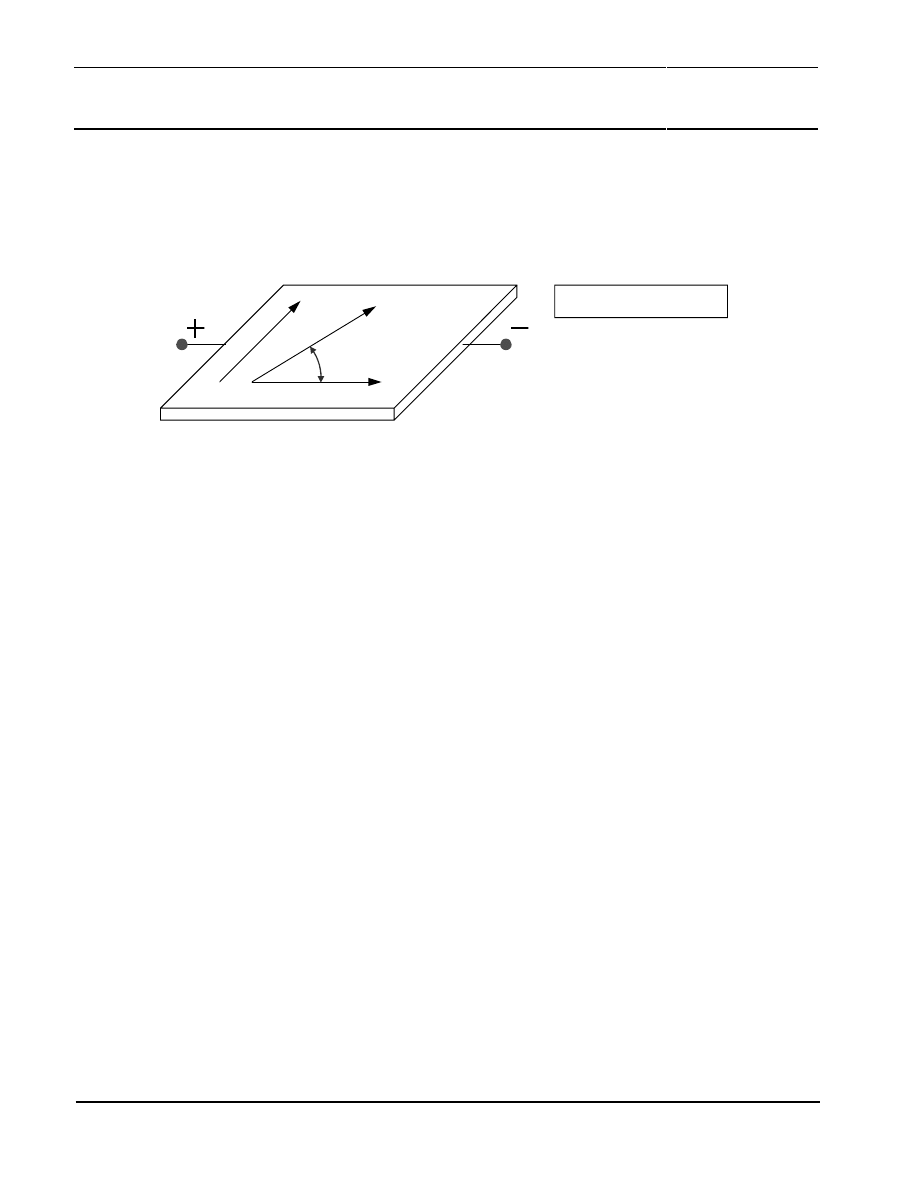
Figure 1 shows a strip of ferromagnetic material, called permalloy.
H
Ma
gn
eti
za
tio
n
Current
Permalloy
α
R = R
0
+
∆
R cos²
α
α
= 0°
Õ
R
max
α
= 90°
Õ
R
min
Figure 1: The magnetoresistive effect in permalloy
Assume that, when no external magnetic field is present, the permalloy has an internal magnetization
vector M parallel to the current flow (
α
= 0). If an external magnetic field H is applied, parallel to the
plane of the permalloy but perpendicular to the current flow, the internal magnetization vector of the
permalloy will rotate around an angle
α
. As a result, the resistance R of the permalloy will change as
a function of the rotation angle
α
, as given by:
R
R
R
=
+
0
0
2
∆
cos
α
(1)
R
0
and
∆
R
0
are material constants. To achieve an optimum sensor characteristics, Philips use
Ni19Fe81, which has a high
R
0
value and low magnetostriction. With this material,
∆
R
0
is in the
order of 2 to 3%. It is obvious from this quadratic equation that the resistance to magnetic field
relation is non-linear. It becomes also clear that the magnetoresistive effect is naturally an angular
effect recommending its utilisation for angle measurement applications. Here the external magnetic
field carries the measurement information between sensor and physical value to be measured.
Having this principle of operation in mind, it becomes clear that the precondition to achieve accurate
measurements is that the internal magnetization vector M must directly follow the vector H of the
external field. This can be achieved by applying an external field H much higher than the internal field
of approximately 3 kA/m. When using the KMZ41 for angle measurement, it is recommended to
provide an external field of at least
H
≥
100 kA / m
(1250 Gauss).
(2)
Philips Semiconductors
Contactless Angle Measurement using
KMZ41 and UZZ9001
Application
Note AN00004
10
In that case the two vectors M and H are virtually parallel to each other.
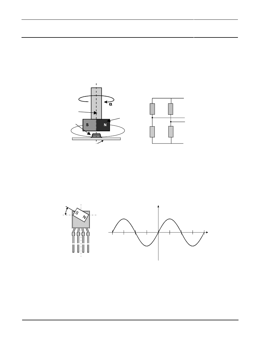
Normally, the external magnetic field is generated by permanent magnets, e.g. SmCo types. Figure 2
shows a basic set-up, where the angular position of a rotating shaft is measured with the help of the
permanent magnet fixed to it.
Rotating Shaft
Permanent
Magnet
PCB / Flex-Foile
Sensor
Wheatstone Bridge
VDD
VSS
R1
R2
R4
R3
+Vo
-Vo
Figure 2 Basic arrangement of sensor and magnet for contactless angle measurement.
The magnetoresistive angle sensors of Philips Semiconductors are etched on a silicon substrate, with
four permalloy strips arranged in a Wheatstone bridge configuration. According to the basic
relationship given by Equation (1), the differential output signal (+Vo, -Vo) of such a Wheatstone
bridge is proportional to
sin 2
α
. This means that a sensor comprising one Wheatstone bridge can
measure an angular range of 90°. This is visualised in Figure 3.
Angle
α
Sensor
Magnet
Signal
Angle
α / °
-180
-90
0
90
180
Figure 3: Output signal from a single Wheatstone bridge sensor
Apart from the limited angular range, the single bridge sensor shows another disadvantage regarding
signal evaluation. As the signal amplitude changes with temperature, the output signal of the sensor
forces the user to implement temperature compensation. This is avoided when using a two-bridge
arrangement combined with a signal evaluation explained below. Figure 4 shows the principle.

Philips Semiconductors
Contactless Angle Measurement using
KMZ41 and UZZ9001
Application
Note AN00004
11
Sensor A
Sensor B
-180 -135 -90 -45 0 45 90 135 180
Signal
angle
α
/ °
Figure 4 Output signal from a double Wheatstone bridge sensor (KMZ41)
The two sensor bridges are positioned at an offset angle of 45° to each other. In this arrangement,
the two output signals show an electrical phase shift of 90°. The two signals are therefore
proportional to
sin 2
α
and
cos2
α
, respectively.
Even in this arrangement, the signal amplitudes will change with temperature. However, both bridges
are processed in the same thin film process steps on the same substrate and they will therefore show
very similar characteristic. Assuming that both output signals have no offsets or offsets have been
compensated previously, the output signals can be described mathematically as follows:
( )
( )
α
α
2
sin
,
0
T
X
T
X
=
(3)
( )
( )
α
α
2
cos
,
T
Y
T
Y
o
=
(4)
Assuming further that the amplitudes of both signals are really identical (
0
0
Y
X
=
), the unknown angle
α
can be determined without any error from the signals
X and Y as given by Equation (5):
=
Y
X
arctan
2
1
α
(5)
This result does not depend on the absolute amplitude of the signals. Consequently, temperature
measurement and compensation of the temperature effects is not required.
Of course, due to the non-ideal manufacturing process, a real sensor will not show the ideal
behaviour assumed above. A detailed discussion of these non-ideal cases and their impact on
system accuracy can be found in section 7.

Philips Semiconductors
Contactless Angle Measurement using
KMZ41 and UZZ9001
Application
Note AN00004
12
3
SYSTEM OVERVIEW
An angle measurement system requires one sensor KMZ41 and one sensor signal evaluation IC
UZZ9001. Figure 5 shows the block diagrams of both components:
Figure 5: Block diagram of the two-chip measurement system
The differential sensor signals +/-Vo1 and +/-Vo2 of the KMZ41 are sampled by the UZZ9001 input
stage and then are converted into the digital domain. This conversion is done with the help of two
separate but simultaneously clocked Sigma-Delta AD converter [4]. The digital representations of the
two signals are then used to calculate the angle. For this calculation the CORDIC algorithm is used.
CORDIC is nothing else than an iterative way to calculate the inverse tangent function of both signals
without extensive numerical overhead. Details of the CORDIC algorithm can be found in reference
[3]. Afterwards, the current angle represented as a 13-bit digital value can be read from the SPI.
As mentioned before, the sinusoidal input signals coming from the KMZ41 may have a static offset
that must be compensated to get accurate results. This compensation is done separately for each
channel by providing an analog voltage to special pins of the UZZ9001. These voltages (OFF1,
OFF2) must be provided continuously during operation as compensation is done real time and not
stored at system start. As KMZ41 and UZZ9001 are not sold as one unit, the user is responsible for
providing the correct compensation voltages. The UZZ9001 provides some special functions for the
trimming process, which are described in section 5.
Apart from the features described above, the UZZ9001 provides an on-chip RC-Oscillator generating
the clock for the IC’s state machine. Consequently, no external clock reference is required for system
operation. Moreover, the UZZ9001 has a power-down and power-up reset with build-in hysteresis.
This reset block automatically generates a reset signal during power-on or if the save voltage range is
left.
KMZ41
14
14
13
13
+Vo1
- Vo1
+Vo2
- Vo2
ADC 1
Algorithm
ADC 2
Adjustment
of
Output
Characteristic
SPI
Interface
Buffer
RC-Oscillator &
Clock Generator
Test and Trim
Mode
RESET
UZZ9001
CS
CLK
DATA
Philips Semiconductors
Contactless Angle Measurement using
KMZ41 and UZZ9001
Application
Note AN00004
13
4 SENSOR
KMZ41
The magnetoresitive sensor KMZ41 of Philips Semiconductors has been designed for angle
measurement applications, preferably in combination with the signal conditioning IC UZZ9001. The
application relevant items are discussed in the following sections. The KMZ41 properties affecting the
system accuracy are discussed in section 7. Please refer to the latest data sheet to get actual
specification data of the KMZ41.
4.1 Layout of the KMZ41 Sensor
The KMZ41 comprises two complete Wheatstone bridges made on the same substrate in thin film
technology. Therefore both bridges show a very good matching regarding electrical and mechanical
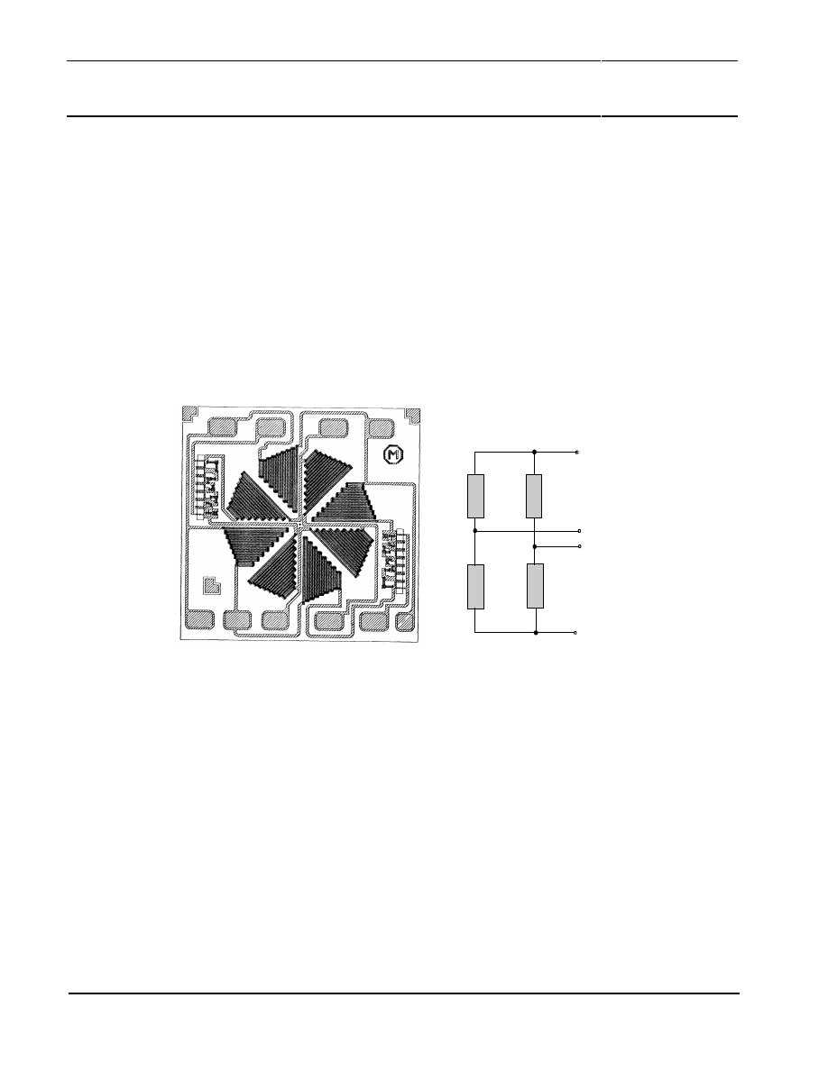
properties. Figure 6 shows the layout of the sensor.
1a
2
1c
1b
1d
2
2
2
Wheatstone Bridge 1
VDDA
VSSA
R1a
R1a
R1b
R1d
R1c
-Vo1
+Vo1
Figure 6: Layout of the double bridge sensor KMZ41.
1a to 1d indicate the sensitive elements of Wheatstone bridge 1
Moreover, the different sensitive elements of Wheatstone bridge 1 are marked. Both bridges have
separate connections for supply voltage. The die size of the KMZ41 is about 1.5 mm
2
with a sensitive
area of about 1 mm
2
.
In order not to influence the external magnetic field and therefore the accuracy of measurements, the
lead frame of the KMZ41 is made without use of ferrous material. Please note that with respect to a
good system design it is also important not to place elements consisting of ferrous material
very close to the KMZ41.
4.2 Input and Output Signals
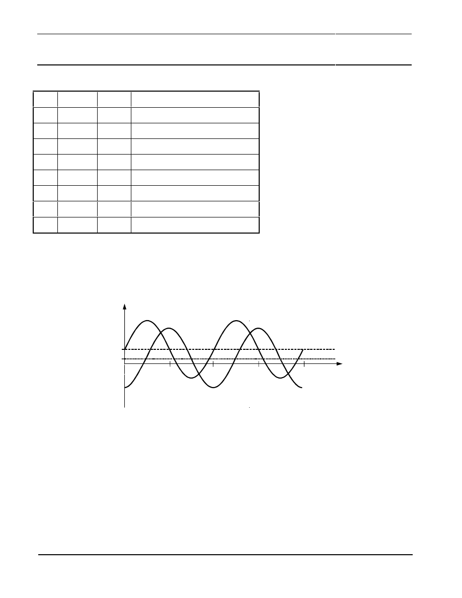
The KMZ41 is housed in a SO8 package. The pinning is given in TABLE 1.
Philips Semiconductors
Contactless Angle Measurement using
KMZ41 and UZZ9001
Application
Note AN00004
14
TABLE 1: Pinning of the KMZ41
Pin
Symbol
Type*
Description
1
-Vo1
A
negative output voltage of bridge 1
2
-Vo2
A
negative output voltage of bridge 2
3
Vcc2
A
supply voltage bridge 2
4
Vcc1
A
supply voltage bridge 1
5
+Vo1
A
positive output voltage of bridge 1
6
+Vo2
A
positive output voltage of bridge 2
7
GND2
A
Ground bridge 2
8
GND1
A
Ground bridge 1
* A = analog pin, D = digital pin
Apart from the two separate supplies, the KMZ41 provides two differential signal lines for each
Wheatstone bridge. The following discussion assumes that the external magnetic field is strong
enough to saturate the sensor. This ensures that each bridge of the KMZ41 has a sinusoidal output
voltage as given in Figure 7.
Voff1
Voff2
Vo1
Vo2
α
90°
180°
270°
360°
0
Figure 7: Output signals of the KMZ41
Ideally, these signals would have no static DC offset. However, static offsets cannot be completely
avoided due to manufacturing tolerances. As these DC-offsets Voff1 and Voff2 affect the system
accuracy, they must be compensated by the signal conditioning IC. The UZZ9001 provides special
build-in functions for this task. Please note that Figure 7 is drawn exaggerated to emphasize the
effect, the actual sensor has much smaller offsets.
The amplitudes of the output signals depend on both the supply voltage and the ambient
temperature. Because of the ideal thermal coupling, the temperature coefficients of both bridges are
almost identical. The MR effect exhibits a negative temperature coefficient. This means that with
higher temperatures, the signal amplitude decreases and vice versa. A short example demonstrates
this effect:

Philips Semiconductors
Contactless Angle Measurement using
KMZ41 and UZZ9001
Application
Note AN00004
15
The typical temperature coefficient (TCVpeak) for the KMZ41 is -0.31 % / K. Consequently, based on
a known peak voltage at room temperature, the peak voltage at any other temperature T can be
calculated as follows:
(
)
°
−
+
=
°
%
100
*
25
1
*
25
TCVpeak
C
T
Vpeak
Vpeak
C
T
(6)
To give an example, the peak voltage of the KMZ41 at room temperature and 5V supply is typically
Vpeak
25°C
= 78 mV. Consequently, at T = 125 °C, a peak voltage of Vpeak
125°C
= 53.8 mV can be
expected. At -40°C, however, the peak voltage increases to Vpeak
-40°C
= 93.7 mV. This effect does not
affect the system accuracy when using the signal processing implemented in the UZZ9001.
Besides the signal amplitude, also the DC offset drifts with temperature. However, this offset drift is
so small that it needs no compensation in normal applications. The offset drift and its impact on
system accuracy are discussed in section 7.
4.3
Magnets and Magnet Arrangements
It is recommended to use the KMZ41 in a magnetic field saturating the sensor. This is guaranteed
when the field strength is above 100 kA/m in the sensitive area of the sensor.
The most simple magnet arrangement is that of a block magnet rotating directly above the KMZ41 as
depicted in Figure 2. The effective magnetic field strength of such a block magnet arrangement
depends on the distance between magnet and sensor, magnet size and magnet material. Because of
strong field requirements, the usage of rare earth magnets such as SmCo or NeFeB is
recommended.
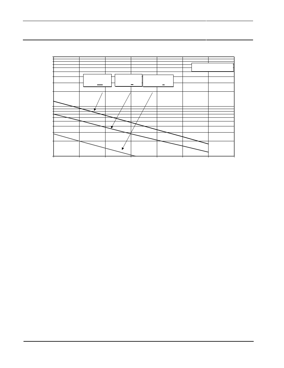
Figure 8 shows the field strength of three sample magnets as a function of the distance between
magnet and the top of the sensor package. It becomes clear that only the SmCo type achieves field
strengths of 100 KA/m and more for distances below 0.8 mm. Its dimension of 8x3x7.5 has been
chosen due to economic aspects and is used in several applications. Stronger fields allowing larger
distances, this can be achieved easily when using thicker but more expensive magnets, e.g. a SmCo
8x4x7.5. Please note that the underlined dimension characterises the direction of magnetization.
In low-end applications, however, a low system price may be more important than excellent system
accuracy. As a consequence, here it may be adequate to use cheaper magnets not saturating the
sensor, e.g. FXD types. The additional error induced by this measure is discussed in section 7.
Philips Semiconductors
Contactless Angle Measurement using
KMZ41 and UZZ9001
Application
Note AN00004
16
Sm
2
Co
17
8 x 3 x 7.5 mm
∆
H
→
3.2 % / 0.1 mm
FXD 330
10 x 7 x 8 mm
FXD 100
8 x 4.35 x 8 mm
10
100
1000
0
1
2
3
4
5
6
7
mechanical air gap in mm
H
in k
A
/m
Figure 8: Field strength in the sensitive plane of the KMZ41 in dependence of the air gap between the top of the sensor
package and the block magnet. The underlined dimension characterises the direction of magnetization.
4.4
Other Mechanical Set-ups
The usage of a block magnet rotating above the sensor is only one simple possibility for a magnetic
system set-up (Figure 2). Meanwhile, several application specific solutions were built. These set-ups
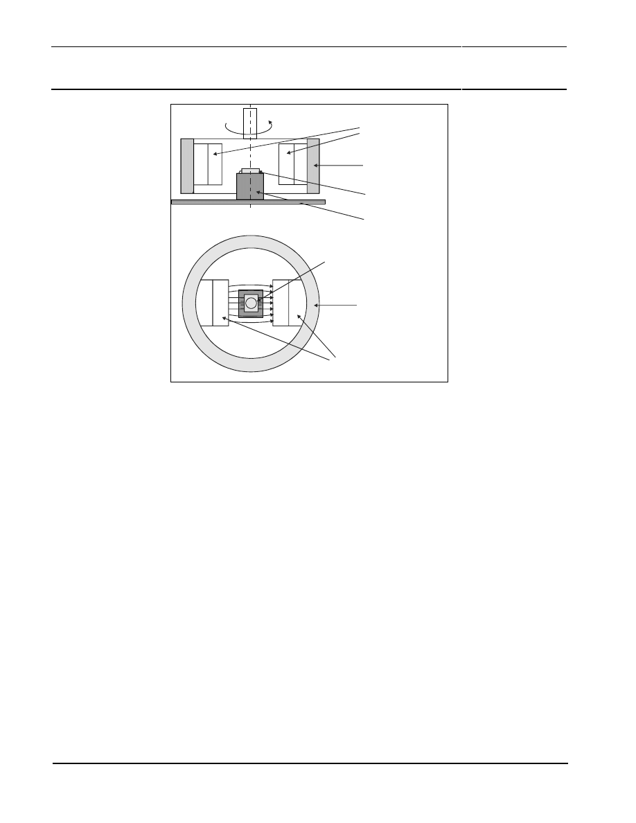
use flux rings and flux guides. Figure 9 shows the general arrangement of such a magnetic system.
The inner walls of the flux ring carry the permanent magnets. This unit rotates around the fixed
sensor (for example KMZ41). The two permanent magnets generate a more homogenous field inside
the ring than the basic arrangement as shown in Figure 2. The additional use of the flux ring makes a
shielding against external fields possible.
Philips Semiconductors
Contactless Angle Measurement using
KMZ41 and UZZ9001
Application
Note AN00004
17
KMZ41 Sensor
Flux ring
Permanent Magnets
SmCo
N
S
S
N
S
N
S N
KMZ41 Sensor
Flux ring,
rotates against
the sensor
Permanent magnets
SmCo
α
Mechanical fixture
free of Fe
Figure 9: Mechanical set-up with two-permanent magnets and a flux ring
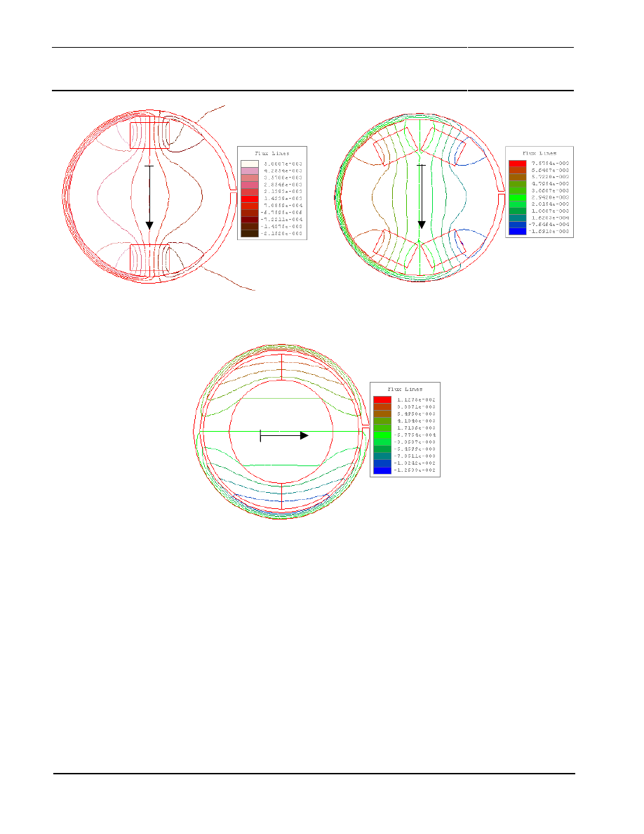
Simulation results of different magnetic arrangements are shown in
•
Figure 10
(two-magnet arrangement),
•
Figure 11
(four-magnet arrangement) and
•
Figure 12
(ring-magnet arrangement).
Each Figure shows the simulated flux lines in dependence of the magnet arrangement. In each
arrangement the same magnetic flux ring and magnetic material is applied (SmCo). The magnetic
arrangements produce different magnetic fields with respect to strength and homogeneity.
It is obvious that the ring-magnet arrangement has the most homogeneous magnetic field in
comparison to the other magnet arrangements. The arrangement with two-magnets seems to be
more inhomogeneous as the four-magnet arrangement.
Philips Semiconductors
Contactless Angle Measurement using
KMZ41 and UZZ9001
Application
Note AN00004
18
x
x
Figure 10: Flux lines of a two-magnet arrangement
Figure 11: Flux lines of a four-magnet arrangement.
x
Figure 12: Flux lines of a ring-magnet arrangement
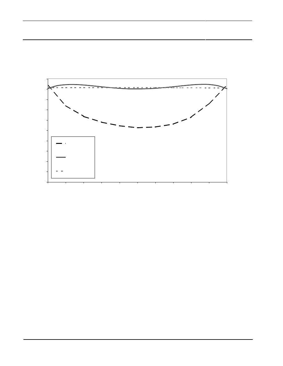
Figure 13 shows the simulated magnetic field strength H of these magnetic arrangements. The
relevant position (X-Position) for the sensor is also shown in Figure 10 to Figure 12.
The ring-magnet arrangement generates the most homogeneous magnetic field in comparison to the
other magnetic arrangements. The arrangement of four-magnets achieves a little bit more
inhomogeneous result as the ring magnet. The simulated magnetic field strength reaches a value up
to H
Simulation
= 180 kA/m and is quite similar between both magnetic arrangements. Overall the four-
magnet arrangement can be an alternative to the ring-magnet arrangement.
The two-magnet arrangement achieves a significant lower magnetic field strength. At the relevant
sensor position a magnetic field strength of H
Simulation
= 105 kA/m is achieved. The parabolic curve is
disadvantageous in comparison to the homogeneous magnetic field of the ring-magnet. Therefore
Philips Semiconductors
Contactless Angle Measurement using
KMZ41 and UZZ9001
Application
Note AN00004
19
this solution can be a compromise between the system accuracy and the system costs. The
mechanical set-up for this simulation is shown in Figure 9.
Figure 13: Simulation of the magnetic field strength H
simulated
for different magnet arrangements (two-, four-magnet and ring-
magnet arrangement)
Therefore the magnet arrangement (diameters, dimensions of the flux ring and the magnets) must be
dimensioned application-specific. The mean targets of optimisation are:
•
Concentration of the magnetic field in order to allow the usage of weaker magnets (ferrite instead
of rare earth).
•
Making the magnetic field homogenous in a wider range to tolerate larger mounting tolerances.
•
Shielding of the primary field against external fields.
A final solution will be a compromise between system accuracy and system costs.
0
20000
40000
60000
80000
100000
120000
140000
160000
180000
200000
0
2
4
6
8
10
12
14
16
18
20
x - position
m
agnet
ic
f
iel
d Hx i
n
A/
m
two-magnets
four-magnets
ring-magnet
W
e
s
e
r /
1800A
nor
d.
x
ls
/
90°
S
tel
lung

Philips Semiconductors
Contactless Angle Measurement using
KMZ41 and UZZ9001
Application
Note AN00004
20
5
SIGNAL CONDITIONING IC UZZ9001
The UZZ9001 is a signal IC for angle calculation. It combines two sinusoidal signals (sine and cosine)
into one digital output signal. The UZZ9001 can be used in conjunction with any sensor that encodes
a mechanical angle into two sinusoidal signals with 90° phase shift. The UZZ9001 is very similar to
the UZZ9000, which is described in the Application note AN98097. Instead of the analog signal
output, the UZZ9001 provides a digital output. The digital output stage implements the Motorola
Serial Peripheral Interface (SPI). Moreover, the UZZ9001 operates in 180° mode only and provides
no possibility to adjust the mechanical offset like the UZZ9000. The UZZ9001 has an overall accuracy
better than 0.35° assuming ideal inputs. This limit holds over the specified ambient temperature range
of -40°C to +150°C. The Pinning of the UZZ9001, the input and output characteristic and the trimming
process are discussed in the following sections.
5.1 General
Description
The basic operation of the UZZ9001 has already been described in section 3. Within this section,
some more details should be addressed that might be useful for a system designer. The detailed
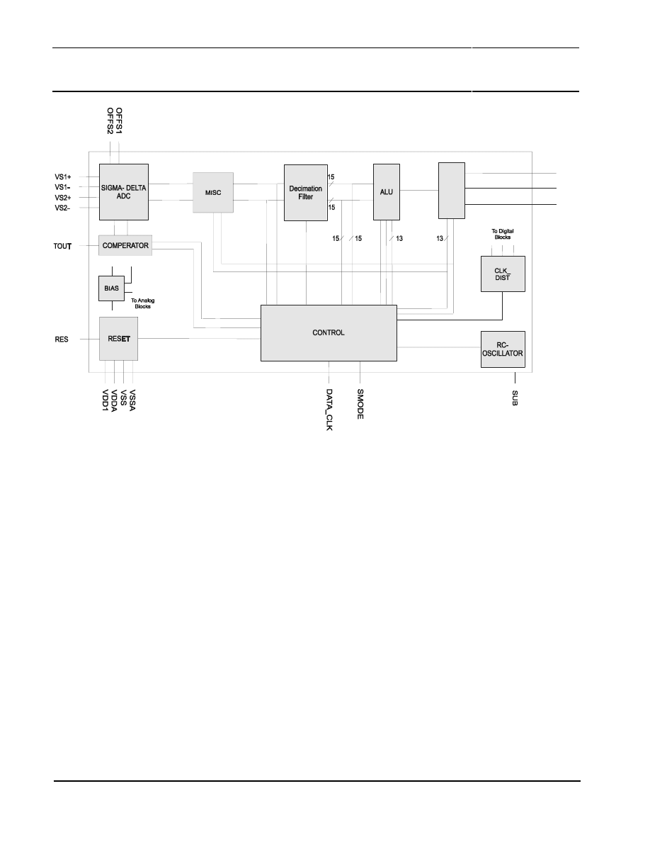
block diagram of the UZZ9001 is given in Firgue 14.
The following list gives a short description of the relevant blocks.
1.
The ADC block contains two Sigma Delta AD converters for the sensor signals and a sensor
offset correction circuitry.
2.
DF stands for the two digital low pass decimation filter which convert the low resolution high
speed bit stream coming from the Sigma Delta converters into a low speed digital word.
3.
The ALU block derives an angle value from the two digital inputs using the CORDIC algorithm.
4.
The SPI converts the digital angle value from parallel into serial data, which can be clocked out
by the user.
5.
The block CNTRL provides the clock and the control signals for the chip.
6.
The COMP block generates binary output signals used for sensor trimming.
7.
The RESET block supplies a reset signal during power-up and power-down when the power
supply is below a certain value.
8.
The OSC unit generates the master clock
Philips Semiconductors
Contactless Angle Measurement using
KMZ41 and UZZ9001
Application
Note AN00004
21
SPI
DATA
CS
CLK
Firgue 14: Detailed block diagram of the UZZ9001
On entering the IC, the analog measurement signals are converted to digital data by an ADC. The
ADC is a Sigma-Delta modulator, employing a 4th order continuous time architecture, with an over-
sampling ratio of 128 to achieve high resolution. The output of the converter is a digital bit-stream at
the over-sampling frequency of typically 500 kHz. The bit stream is fed into a decimation filter, which
performs both low-pass filtering and down sampling. There are two input channels of the IC, each of
which has its own ADC and decimation filter. The two decimation filter outputs are digital words of 15-
bit at a lower frequency of typically 3.9 kHz. This is the typical sampling frequency of the sensor
system. The digital representations of the two signals are then used to calculate the current angle.
This calculation is done using the so-called CORDIC algorithm. The angle is represented with a 13-bit
resolution accessible via the SPI (Serial Peripheral Interface).
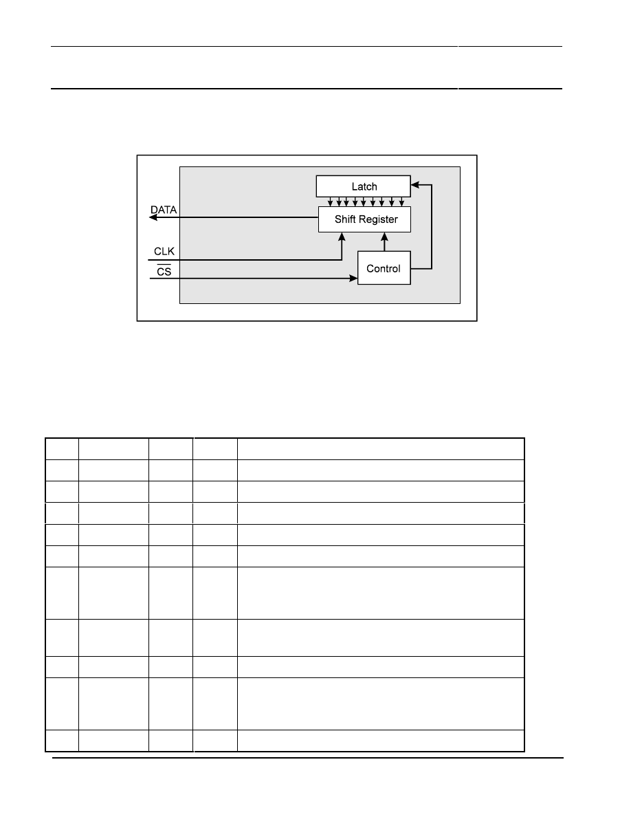
The SPI is a byte-orientated synchronous serial master-slave bus system. The UZZ9001 has a SPI
that operates in slave mode only. A configuration of the UZZ9001 via the SPI is not possible and
therefore an input data line is not required.
The general arrangement of such a basic slave SPI interface is shown in Figure 15. All signals are
related to the common VSS line (digital ground). Only a master SPI module (Electronic Control Unit,
ECU) can initiate transmissions. Therefore, the start of the transmission is indicated by setting the CS
pin to logical low (signal is active low), by the master module. Then the master module can “clock out”
Philips Semiconductors
Contactless Angle Measurement using
KMZ41 and UZZ9001
Application
Note AN00004
22
the required data from the shift register. This transfer mode and details of the timing are specified in
section “Serial Peripheral Interface (SPI)”.
Figure 15: Slave-SPI Block Diagram
5.2 Pinning of the UZZ9001
The following Table 2 gives the pinning of the UZZ9001 that comes in a standard SO24 package.
Table 2 Pinning of the UZZ9001
Pin
Symbol
I/O*
Type*
Description
1
+Vo2
I
A
positive output voltage of sensor 2 (Wheatstone bridge 2)
2
+Vo1
I
A
positive output voltage of sensor 1 (Wheatstone bridge 1)
3
VDD
S
A
digital supply
4
VSS
S
A
digital ground
5
VSSA
S
A
analog
ground
6
RES
I
D
resets the digital part of the UZZ9001, pin is active high. If
not used, pin can be left unconnected (internal pull-down
resistor) or connect it to ground.
7
TEST1
I
D
used for production tests, can be left unconnected (internal
pull-down resistor) or connect it to ground
8
TEST2
O
D
used for production tests, must be left unconnected
9
DATA_CLK
I
D
data clock, used when setting the UZZ9001 into trim mode,
can be left unconnected (internal pull-down resistor) or
connect it to ground
10
SMODE
I
D
serial mode programmer, used when setting UZZ9001 into

Philips Semiconductors
Contactless Angle Measurement using
KMZ41 and UZZ9001
Application
Note AN00004
23
Pin
Symbol
I/O*
Type*
Description
trim mode, can be left unconnected (internal pull-down
resistor) or connect it to ground
11
TEST3
O
D
used for production tests, must be left unconnected
12
DATA
O
D
DATA pin of the SPI.
13
CLK
I
D
Data clock of the SPI.
14
CS
I
D
Chip Select of the SPI.
15
OFF2
I
A
offset trimming input for sensor 2 (Wheatstone bridge 2)
16
OFF1
I
A
offset trimming input for sensor 1 (Wheatstone bridge 1)
17
VDDA
S
A
analog
supply
18
VSSA
S
A
analog
ground
19
TEST4
I
D
used for production tests, can be left unconnected (internal
pull-down resistor) or connect it to ground
20
TEST5
I
D
used for production tests, can be left unconnected because
of an internal pull-down resistor or connect it to ground
21
VDD
S
A
digital supply
22
TOUT
O
D
used in trim mode, gives the offset corrected signal of sensor
1 or sensor 2, must be left unconnected in application
23
-Vo2
I
A
negative output voltage of sensor 2 (Wheatstone bridge 2)
24
-Vo1
I
A
negative output voltage of sensor 1 (Wheatstone bridge 1)
* A = analog pin, D = digital pin, S = supply, I = input, O = output
5.3 Characteristics of the Input Signals
The input stage of the UZZ9001 expects two sinusoidal signals (section 4.2). The electrical
characteristics of these signals are defined in TABLE 3. These values correspond to the KMZ41
sensor specification.
TABLE 3: Limits of the UZZ9001 input signals
Parameter
Min
Max
Units
Analog supply voltage
4.5
5.5
V
Differential input voltage range (peak voltage)
+/- 6.6*
+/- 28
mV / V

Philips Semiconductors
Contactless Angle Measurement using
KMZ41 and UZZ9001
Application
Note AN00004
24
Parameter
Min
Max
Units
referred to analog supply voltage
(including any offset)
Differential input voltage offset referred to analog
supply voltage
-2
+2
mV / V
Common mode range referred to the analog
supply voltage
490
510
mV / V
* If signals of both channels are below this limit at the same time, the magnet lost error condition
becomes active (see section 5.6).
5.4 Characteristic of the Output Signal (SPI-Pins)
The digital output signal of the UZZ9001 is coded in 14 bits named D13 to D0. Within these 14 bits,
the coding of the angle uses 13 bits (D12 to D0). One bit (D13) is reserved to indicate error and
diagnostic conditions.
The 14 data bits (D13-D0) are arranged in 2 Bytes as shown in Figure 16. D13 is the MSB of the
sensor signal and D0 is the LSB of the sensor signal. Byte 2, which is sent first, contains the data bits
D13 to D7 and additionally the parity bit P2 which is added to allow the recognition of disturbed
messages. P2 gives the ODD Parity of the data bits D13 to D7 and has to be evaluated by the master
module.
Figure 16: Coding of the digital output
Similar, Byte 1 comprises data bits D6 to D0 and the parity bit P1, which gives the ODD Parity of the
data, bits D6 to D0. The ODD parity is chosen to detect failure modes where the DATA pin is short-
circuit to GND or VDD or where the connection between DATA out of the slave and DATA in of the
master is interrupted (e.g. broken wire).
The error and diagnostic conditions are indicated by D13 = 1 (logical high). In this case, the last two
bits (D0 and D1) specify the error case. All other bits (D3 - D12) still shows the current measurement
value. Consequently, the two least significant bits are lost for the measurement representation, which
results in 11-bit resolution in error and diagnosis cases. Whether the measurement value is reliable or

Philips Semiconductors
Contactless Angle Measurement using
KMZ41 and UZZ9001
Application
Note AN00004
25
not depends on the special error case and has to be evaluated by the master unit. The coding is
specified in Table 4.
Table 4: Coding of error and diagnostic cases
D1
D0
Case
Measurement value
reliable
Comments / Remarks
0
0
No valid value presently available
due to RESET
No
0
1
Magnet Lost
No
1
0
reserved
-
1
1
reserved
-
The output stage of the UZZ9001 (DATA pin) is able to drive any external output load as defined in
TABLE 5. This output changes from direct connection to VSS to output active (driver active) in
dependence of the CS line.
TABLE 5: Static Operating Characteristics of the DATA Pin
Symbol
Parameter
Min
Nom
Max
Units
V
OL
Output voltage “LO”
0.4
V
V
OH
Output voltage “HI”
V
DD
- 0.8
V
DD
V
I
O
Output current
(Peak Driver Capability)
10
mA
C
OUT
Output capacitance (
Note1)
150
pF
Note 1: C
OUT
should chosen adequately in combination with a resistance in order to limit I
O
during switching to the specified
maximum value
The requirements of the other digital signals (CLK and CS pins) of the SPI are given in Table 6. This
signals are input signals of the SPI and necessary for the digital output signal on the DATA Pin.
Table 6 Static Operating Characteristics of CLK and CS Pins
Symbol
Parameter
Min
Typ
Max
Unit
V
IL
Input voltage “LO”
0
0.3 * V
DD
V

Philips Semiconductors
Contactless Angle Measurement using
KMZ41 and UZZ9001
Application
Note AN00004
26
V
IH
Input voltage “HI”
0.7 * V
DD
V
DD
V
I
I
Input current
10
uA
C
IN
Input capacitance
10
pF
5.5 Serial Peripheral Interface (SPI)
This chapter gives a general overview on the pin characteristics, their interrelationships and timing
requirements.
5.5.1 CS Pin
The Electronic Control Unit (ECU) selects the UZZ9001 via the CS pin, which is active low. Whenever
the pin is in a logic low state, the DATA pin output driver is enabled allowing data to be transferred
from the UZZ9001 to the ECU. Consequently, on the falling edge of the CS signal, the DATA output
driver changes from fixed connection to Vss into active mode which means it drives the actual data
bit level onto the DATA line. CS is active (low) during data transmission. With the leading edge of CS,
DATA changes again from active state to fixed connection to Vss. Additionally the edges on the CS
line are used to up-date the SPI Shift Register content.
5.5.2 CLK
Pin
The system clock (CLK) clocks the internal shift registers of the UZZ9001. With every falling edge of
CLK, the register is shifted by one position and therefore the next data bit level is driven on the DATA
line. The bit level is sampled (by the master) at the next leading edge of the CLK signal. Due to
synchronisation requirements of the internal logic of the UZZ9001 and to ensure correct SPI timing
conditions, the CLK pin must be held on a constant “logical high” level whenever a transition of the
CS signal occurs. The master unit provides the timing of the CS and CLK Signal, therefore the
designer of the ECU is responsible for meeting these timing requirements. Details of the SPI Timing
are specified in section “SPI-Timing” (5.5.4).
5.5.3 DATA Pin
The serial output (DATA) pin is the output from the shift register. It operates as push-pull driver. If CS
is not active, the pin is connected to Vss. An external serial resistor will limit the current if
inadvertently the line is connected to VDD. The DATA pin remains in this state until the CS pin goes
to a logic low state. When CS is active then the DATA pin push-pull output driver is activated and
drives the present data bit level onto the bus line.
Philips Semiconductors
Contactless Angle Measurement using
KMZ41 and UZZ9001
Application
Note AN00004
27
5.5.4 SPI-Timing
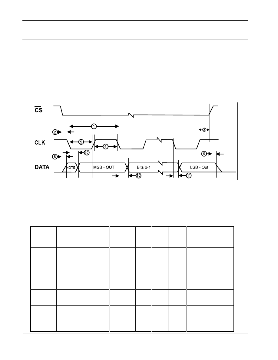
As a slave node the UZZ9001 provides only one operation mode. With respect to Motorola SPI
devices, this mode is selected by setting CPHA = 1 and CPOL = 1.
In this transfer mode the data bits are sampled by the master unit using the leading edge of the clock,
as shown in Figure 17. The falling edge indicates that the next data bit has to be provided by the
slave device (shift operation).
NOTE: Not defined data, normally LSB of character previously transmitted
Figure 17: UZZ9001 SPI Interface Timing
The timing requirements of the SPI interface are given in the following table:
TABLE 7: SPI-Timing:
Diagram
Number
Parameter
Symbol
Min
Max
Unit
Remarks / Test
Conditions
Operating Frequency
f
op
DC
1
MHz
1
Cycle Time
t
cyc
1
-
us
2
Enable Lead Time
t
Lead
15
ns
Determined by
master module
3
Enable Lag Time
t
Lag
15
ns
Determined by
master module
4
Clock High Time
t
clk_high
100
-
ns
Determined by
master module
5
Clock Low Time
t
clk_low
100
-
ns
Determined by
master module
8
Access Time
t
acc
0
20
ns
Time to data active

Philips Semiconductors
Contactless Angle Measurement using
KMZ41 and UZZ9001
Application
Note AN00004
28
Diagram
Number
Parameter
Symbol
Min
Max
Unit
Remarks / Test
Conditions
from fixed V
SS
state
9
Disable Time
t
dis
-
25
ns
Hold time to fixed
V
SS
state
10
Data Valid Time
(After Clock Edge)
t
v
-
40
ns
With 100 pF on all
SPI pins
11
Data Hold Time
(Output, After Clock
Edge)
t
h
5
-
ns
Transmission Delay
(Time between the
leading edge of CS
until the next falling
edge)
t
Delay
1.2
us
Another advantage of the chosen operation mode is that the CS pin has not to be toggled between
the transmission of more than one byte. This lightens the two byte operation of the UZZ9001 as
explained below. The timing of the CS line during transmission of the two sensor bytes is shown in
Figure 18.
Figure 18: Timing of the CS Line
The transmission may be stopped by the user at any time. A leading edge at the CS pin will initialise
the SPI Shift Register allowing the start of a complete new transmission. If the CS line is held low
(active) during stop of transmission, the stopped transmission can be continued without loss of data.
5.6 Offset Trimming
For a correct output signal, it is necessary to adapt the offsets of the two input signals to the input
stage of the UZZ9001. For this reason a sensor offset cancellation procedure was implemented in the
Philips Semiconductors
Contactless Angle Measurement using
KMZ41 and UZZ9001
Application
Note AN00004
29
UZZ9001 which is started by sending a special serial data protocol to the UZZ9001. This trimming
procedure is required for both input signals.
5.6.1 Trim Interface
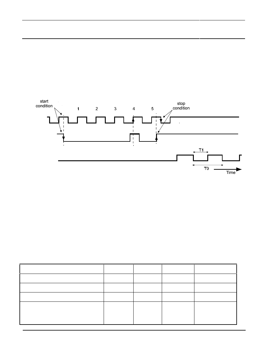
The serial interface used to switch the UZZ9001 into trim mode consists of the two terminals SMODE
(pin 10) and DATA_CLK (pin 9). The structure of this protocol is shown in Figure 19.
Statusbit #
DATA_CLK
(input at pin 9)
SMODE
(input at pin 10)
TOUT
(output at pin 22)
Figure 19: Protocol used to set the UZZ9001 into trim mode.
All signal levels at DATA_CLK and SMODE must be chosen according to the requirements listed in
TABLE 8. Because of the asynchronous protocol, the following points have to be taken into account:
The protocol starts with a falling edge at SMODE, which must occur at a high level of the DATA_CLK.
The next five bits are used for coding of the message send to the UZZ9001. They are transferred via
SMODE and are sampled with the rising edge of DATA_CLK. During the fifth high level output of
DATA_CLK (counted from the start condition onwards), a rising edge must appear at SMODE and
afterwards DATA_CLK has to change one more time to low level in order to successfully complete
the protocol.
TABLE 8: Definition of the trim interface signals
Parameter
Min
Nom
Max
Unit
supply voltage VDD of UZZ9001
4.5
5.0
5.5
V
low level of DATA_CLK, SMODE
0
5
%VDD
high level of DATA_CLK, SMODE
95
100
%VDD
rise and fall time of signal edges of
DATA_CLK and SMODE
(from 10% VDD to 90% VDD and
8
ns

Philips Semiconductors
Contactless Angle Measurement using
KMZ41 and UZZ9001
Application
Note AN00004
30
Parameter
Min
Nom
Max
Unit
vice versa)
Frequency of DATA_CLK
0.1
1
MHz
5.6.2 How to Enter the Trim Mode
The status bits to be transmitted to the UZZ9001 are shown in TABLE 9. Also please note that a
complete protocol has to be sent to return to normal operation. Another possibility to leave the trim
mode is to reset the device.
TABLE 9: Programming of trim modes
Mode
Status Bits
1
2
3
4
5
enter trim mode for sensor input
channel 1
0
0
0
1
0
enter trim mode for sensor input
channel 2
0
0
1
0
0
leave trim mode for either input
channels
0
0
0
0
0
After entering one of the trim modes, a square wave output is visible at the terminal TOUT (pin 22)
provided there is a dynamic input signal.
5.6.3 Offset
Calibration
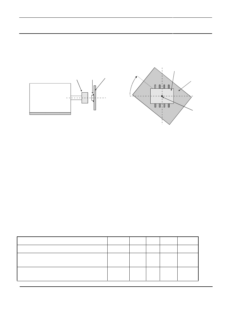
To make use of the build-in trimming procedure of the UZZ9001, it is necessary to generate dynamic
sensor signals at its inputs. When the KMZ41 is used, a rotating permanent magnet in front of the
sensor can easily generate these input signals. The principle of this set-up is shown in Figure 20.
Please note that the absolute rotational speed of the permanent magnet is not that important but it
must be constant over time. Please further note that the rotational axis of the motor and magnet must
be aligned exactly with the center of the KMZ41 package as shown in Figure 20. It is not necessary to
use the same magnet for both trimming and application, but after trimming, the KMZ41 and UZZ9001
must be treated as one unit. The trimming procedure is as follows.
When the UZZ9001 has been switched to trim mode and sinusoidal sensor voltages are applied to its
inputs, then the terminal TOUT (pin 22) immediately shows a square wave signal. This square wave
Philips Semiconductors
Contactless Angle Measurement using
KMZ41 and UZZ9001
Application
Note AN00004
31
signal has the same frequency as the sensor signal and a duty cycle T1/T0 as shown in Figure 19
previously.
Sensor
(KMZ41)
Permanent-Magnet
Rotating with
Axis of Rotation
DC-Motor
Permanent-Magnet
Sensor
(KMZ41)
PCB
ω
ω
Figure 20: Proposal for a mechanical set-up to trim the UZZ9001
At a duty cycle of 50%, the offset for the selected channel is virtually eliminated. Therefore, the
voltage at OFF1 (PIN16, channel 1) or OFF2 (PIN15, channel 2), respectively, has to be adjusted
until this target is achieved. The trimming voltages OFF1 and OFF2 must be ratiometric to the
UZZ9001 VDDA supply and must not vary more than 0.1 % VDDA with temperature and over lifetime.
As already proposed for adjusting the angular ranges and zero point offset, these properties can be
ensured, for example, when using a trimmable resistor divider connected to VDDA.
When building up an automatic trimming station for mass production, it is recommended to firstly
determine the actual trim voltage to be fed to OFF1 and OFF2 as a fraction of VDDA. Afterwards, the
resistor dividers are trimmed according to the requirements found. This procedure will be much faster
compared with trying to trim the resistors step by step to get 50% duty cycle. In practice, laser
trimmable resistors used for both divider elements have shown good results. Using resistors of the
same material is important to get a similar temperature coefficient. Please note that for duty cycle
measurements, the measuring device should be set into averaging mode in order to eliminate the
influence of short spikes or noise. TABLE 10 summarises the recommended trim parameters:
TABLE 10: Definitions and recommendations of trim parameters
Parameter
Symbol
Min
Nom
Max
Unit
Frequency of the motor
fo
20
30
s
-1
Frequency of the sensor input signals
(KMZ41)
2 fo
40
60
Hz
Stability of the rotational speed over one
signal period
∆
f
0.05
% fo

Philips Semiconductors
Contactless Angle Measurement using
KMZ41 and UZZ9001
Application
Note AN00004
32
Parameter
Symbol
Min
Nom
Max
Unit
Limits for the duty cycle of nominal 50%
during trimming
49.96
50.04
%
Variation of the voltages provided at OFF1
and OFF2 with temperature and during
lifetime
0.1
%VDDA
Voltage range for OFF1 and OFF2
33.3
66.7
%VDDA
Input signal offset range to be aligned by
OFF1 and OFF2. Values are referred to
VDDA. The min value corresponds to the
min value for OFF1 and OFF2 (33.3%
VDDA), and vice versa.
-2
2
mV / V
Example:
The following example serves to demonstrate the meaning of these limits and allows the calculation
of the system accuracy if other values are applied.
Assuming sinusoidal sensor signals with the amplitude
A, then the relation between an DC offset
∆
x
and the measured duty cycle T1/T0
is as follows:
(
)
(
)
0
/
1
5
.
0
sin
T
T
A
x
+
⋅
=
∆
π
(7)
At room temperature and 5V supply voltage, the typical signal amplitude
A of the KMZ41 is 78 mV.
Consequently, at a duty cycle of 50.04% (or 49.96%) the remaining offset voltage is:
(
)
(
)
mV
mV
x
098
.
0
5004
.
0
5
.
0
sin
78
−
=
+
⋅
=
∆
π
(8)
As a result, the remaining offset is 0.13% referred to the signal amplitude of 78 mV. The angular error
caused by this offset is discussed in section 7.
The other parameter specified is the drift of the voltages applied to OFF1 and OFF2 with temperature
and over lifetime. It is specified to be less than 0.1% VDDA. The maximum voltage range for OFF1
and OFF2 is 33.3 % VDDA which is used to align the input signal offset range of +/- 2 mV / V.
Consequently, changes of OFF1 or OFF2 by 0.1% VDDA will cause offset voltages
∆
x of:

Philips Semiconductors
Contactless Angle Measurement using
KMZ41 and UZZ9001
Application
Note AN00004
33
V
/
mV
012
.
0
V
/
mV
2
2
VDDA
%
3
.
33
VDDA
%
1
.
0
=
⋅
⋅
=
∆
x
(9)
At a supply voltage of 5V, the offset voltage caused by the drift of OFF1 and OFF2 is 0.06 mV for
each channel. The resulting angular error due to this offset is discussed in section 7.
5.7 Reset
In addition to the external reset pin (pin 6), the UZZ9001 provides an internal power-up / power-down
reset logic which supervises the supply voltage continuously. When the supply voltage increases and
reaches a safe level, reset becomes inactive and the device starts initialization after a nominal delay
of 100 us. This is to ensure settling of all analog and digital sections. When the supply voltage leaves
the safe voltage level, the device is reset immediately. This internal reset logic can be over-ridden by
the external pin RES (pin 6) in all modes and at any time. The reset pin RES (pin 6) is active high. It
is internally pulled down to VSS and therefore does not have to be connected if the function is not
required.
As the UZZ9001 has two different voltage supplies, the power-up and power-down reset operates as
follows:
1.
Power-Up
VDD or VDDA
<= 2.8 V
reset active
VDD and VDDA
>= 4.5 V
reset not active, reset will switch from high
to low after a delay of 100 us.
2.
Power-Down
VDD or VDDA
<= 2.8 V
reset active
VDD and VDDA
>= 4.4 V
reset not active, device active
If the supply voltage rises, the device is switched into active mode as soon as VDD
AND VDDA
reach the power-up switching level, which lies between 2.8 V and 4.5 V, and the delay of about
100 us has elapsed. In contrast, if the supply voltage at VDD
OR VDDA goes below the power-down
limit, which lies between 2.8 V and 4.4 V, reset becomes active immediately. Due to possible ripples
on the supply voltage, a hysteresis of at least 100 mV is implemented between the power-up and
power-down switching voltage levels. The following TABLE 11 summarises the specified limits.
TABLE 11: Definitions of switching levels of the build-in reset logic
Parameter
Min
Typ
Max
Unit
Switching voltage for falling VDDA OR VDD
2.8
4.4
V

Philips Semiconductors
Contactless Angle Measurement using
KMZ41 and UZZ9001
Application
Note AN00004
34
Parameter
Min
Typ
Max
Unit
Switching Hysteresis
0. 3
V
Switching voltage for rising VDDA AND VDD
2.8
4.5
V
Delay for starting the initialization of the UZZ9001 when VDD AND
VDDA have risen above the power-up switching level
100
us
5.8 Measurements
Dynamics
The UZZ9001 provides an on-chip RC Oscillator that generates the clock for the whole device.
Consequently, no external clock supply is required for the measurement system.
The nominal clock frequency of the on-chip oscillator is 4 MHz at room temperature. It varies over
temperature. At -40°C, the clock frequency may reduce down to 2.3 MHz. At higher temperatures,
however, a frequency up to 5.7 MHz may occur. Consequently, this influences the dynamics of
measurements. From the application point of view, two different effects have to be distinguished: The
system delay, which means how long it takes until a changed input signal is recognized at the output,
and the measurement update rate.
The system delay is mainly caused by the settling time of the low pass decimation filter, which
depends on the maximum frequency content (shape) of the input signals and the clock frequency.
The following maximum values can be expected for the entire system delay (see TABLE 12):
TABLE 12: System delay and update rates of the UZZ9001
Parameter / Conditions
Min
Typ
Max
Unit
System delay defined as the time passes by
until 95% of the final value is reached:
-
Max. signal frequency < 200Hz
-
Transients (Step response)
0.6
1.2
ms
ms
Measurement update rate:
-
-40°C
-
25°C (room temperature)
-
150°C
0.45
0.26
0.18
ms
ms
ms
The measurement update rate, however, is directly related to the oscillator frequency. At room
temperature, a new value is available every 0.26 ms. When looking at the entire temperature range of
the UZZ9001, update rates between 0.45 ms and 0.18 ms are possible (see TABLE 12).
Philips Semiconductors
Contactless Angle Measurement using
KMZ41 and UZZ9001
Application
Note AN00004
35
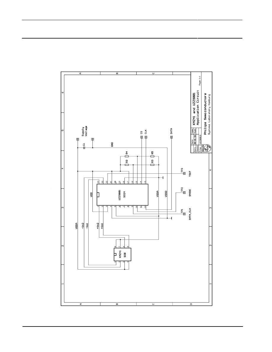
5.9 Typical Application Circuit
Figure 21 shows a typical application circuit.
Figure 21: Schematics of a typical application circuit

Philips Semiconductors
Contactless Angle Measurement using
KMZ41 and UZZ9001
Application
Note AN00004
36
6 SYSTEM
ACCURACY
6.1 Sensor KMZ41
There are three different errors that may be caused by non-adequate magnetic field arrangements.
These are:
•
Form deviations of the sensor signals (no sinusoidal shape) and hysteresis of the sensor
response if the magnetic field H does not saturate the sensor.
•
Form deviations of the sensor signals caused by a non-symmetrical sensor to magnet
arrangement (inhomogeneous magnetic field).
•
Influence of external magnetic fields influencing the primary field used for measurements.
The influence of external fields can not be described in general as these effects depend on the actual
measurement set-up. Therefore this item is not discussed within this paper. The only possibility to get
rid of external fields or to limit its impact is to use some kind of a magnetic shielding as discussed in
section 4.
In addition to these magnetic effects, there are some non-ideal properties of the KMZ41 sensor
affecting the system accuracy. These are discussed in section 7.1.3.
6.1.1 Less Magnetic Field Strength
A complete saturation of the sensor would require the usage of an infinite magnetic field.
Consequently, a complete saturation is impossible in practice and errors caused by fewer magnetic
fields have to be taken into account. The magnetic field strength, which is proposed in this paper, is a
compromise between the remaining error and magnet costs.
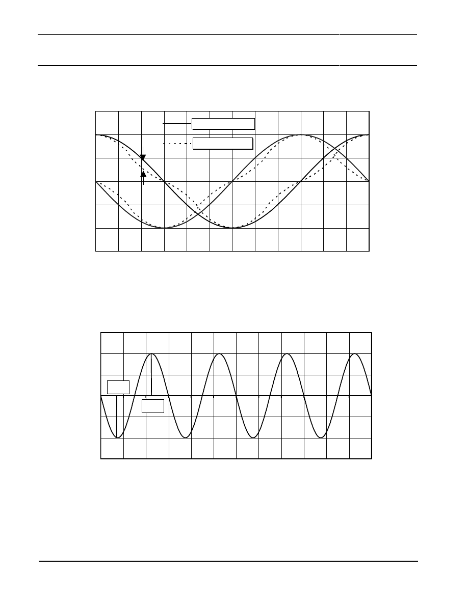
Insufficient magnetic field has two effects. The first one is the signal form error caused by a non-
sinusoidal shape of the output signals (see Figure 22). Figure 23 shows the shape of the resulting
measurement error. Due to its geometrical nature, the maximum and minimum values will always
occur at the same locations for every sensor. Maximum values occur at the mechanical angles of
11.25°, 33.75°, 56.25°, 78.75°, 101.25°, 123.75°, 146.25° and 168.25°. No measurement errors occur
at 22.5°, 45°, 67.5°, 90°, 112.5°, 135°, 157.5° and 180°.
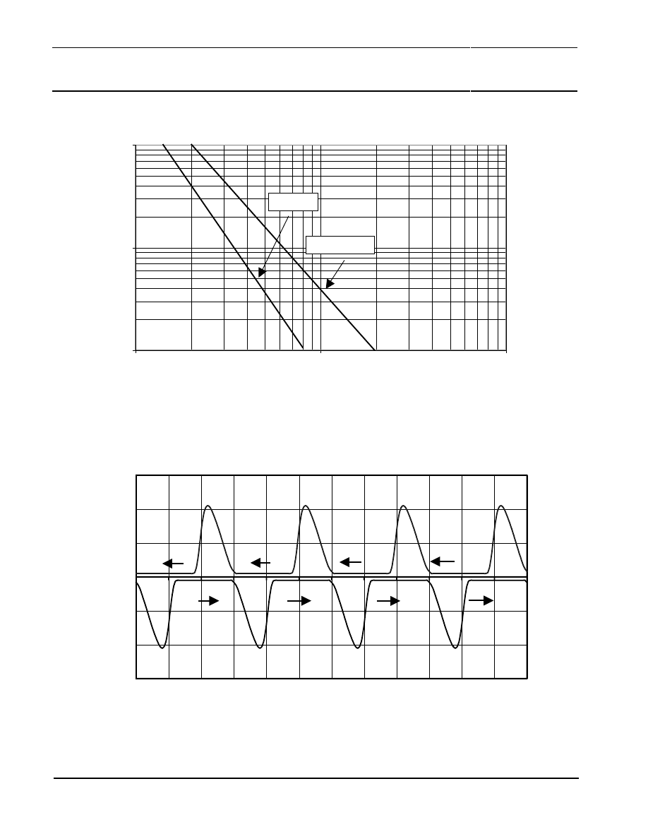
Figure 24 shows the relation between the magnetic field strength H and the maximum peak error
E
Form
that may occur. At the recommended magnetic field strength of 100 kA/m, the measurement
error is less than E
Form
= 0.04° and therefore negligible. The signal form error is reversible and does
not depend on the history, as it is the case for hysteresis effects.
Hysteresis effects become visible if the angle turns back and forth over larger angular ranges as
shown in Figure 25. The positions where these errors occur depend on the direction of movement. If
fields become stronger, the hysteresis zones shrink to smaller areas around the positions 0°, 45°, 90°
and 135°. Figure 24 also gives the maximum error caused by hysteresis effects. These are less than
the errors caused by the signal form error.
Philips Semiconductors
Contactless Angle Measurement using
KMZ41 and UZZ9001
Application
Note AN00004
37
sinusoidal response
∆
V
deformed response
0
15
30
45
60
75
90
105
120
135
150
165
180
Angle
in Degrees
Vo
1, Vo
2
Figure 22: Signal form error of KMZ41 output signals caused by too low magnetic field not saturating the sensor
33.75
11.25
0
15
30
45
60
75
90
105
120
135
150
165
180
Angle in Degrees
E_Form
Figure 23: Shape of the measurement errors caused by the non-ideal sensor signals given in Figure 22.
Philips Semiconductors
Contactless Angle Measurement using
KMZ41 and UZZ9001
Application
Note AN00004
38
hysteresis
form deviation
0,01
0,1
1
10
100
1000
External Magnetic Field H in kA/m
E
_
max i
n
D
e
grees
Figure 24: Maximum measurement error caused by signal form error and hysteresis
0
15
30
45
60
75
90
105
120
135
150
165
180
Angle in Degrees
E_Hysteresis
Figure 25: Shape of the measurement error caused by hysteresis
Philips Semiconductors
Contactless Angle Measurement using
KMZ41 and UZZ9001
Application
Note AN00004
39
It is obvious that the measurement error caused by signal form errors and hysteresis can be
neglected when using a magnetic field around 100 kA/m.
Another argument for using strong magnetic fields is the lower impact of external magnetic fields.
This is especially an issue when using an unshielded magnet set-up. Here, even the very small
magnetic earth field of about 30 A/m causes measurement errors. To give a rough estimation, an
earth field perpendicular to the measurement field of 100 kA/m would cause a maximum error of
0.017°. Ten times this error would occur when operating at 10 kA/m, and this is not negligible.
6.1.2 Effects of Inhomogeneous Magnetic Fields
The sensor signal will get deformed even if sensor and magnet are not precisely aligned, which also
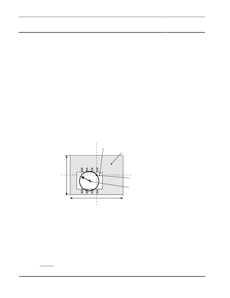
may cause measurement errors. The reason for these deformations is that then the sensitive part of
the sensor is not completely placed in the homogeneous part of the magnetic field, or, in other words,
the relevant part of the magnetic field used for measurements has become inhomogeneous. As the
actual angular error resulting from an inhomogeneous field depends on the specific set-up, it can not
be calculated in general. However, for the simple block magnet arrangement discussed before, a rule
of thumb can be used.
Sensor
Magnet
Real axis of rotation
R
w
l
Ideal axis of rotation
Figure 26: Definition of parameters for calculating the angular error caused by an inhomogeneous field.
Assuming the magnet arrangement depicted in Figure 2, the resulting maximum angular error can be
estimated as given in Equation (10):
2
eu
Inhomogeno
R
C
E
s
⋅
=
(10)
with:
(
)
2
320
l
w
C
+
°
=
Magnet Constant

Philips Semiconductors
Contactless Angle Measurement using
KMZ41 and UZZ9001
Application
Note AN00004
40
R
Radius of the circle in which the centre of the magnet lies (see Figure 26).
The midpoint of this circle is identical with the ideal axis of rotation
w
Width of the magnet
l
Length of the magnet
Note that w and l describe the magnet surface faced to the sensor. For the above mentioned
magnets (see Figure 8), w and l are approximately 8 mm and thus
2
mm
/
25
.
1
°
≈
C
. Consequently, a
radius R of 1 mm (the magnet is positioned 1 mm apart from the ideal position) can cause maximum
errors up to 1.25°. As a result, small mounting tolerances are strongly recommended when using a
simple block magnet arrangement. However, enlarging the magnet will reduce this error at the
expense of higher magnet costs.
Please note that this error calculation is only applicable for the block magnet arrangement. When
looking at more complex magnetic designs, e.g. the one depicted in Figure 9, a customised solution
must be found. Normally, when carefully designing such a complex magnetic circuit, higher mounting
tolerances are possible.
Also a non-parallel position of the sensor surface and magnet surface causes errors due to an
inhomogeneous magnetic field in the sensitive area of the sensor. But as long as this deviation can
be limited to the range of 1° to 2°, the resulting measurement error is negligible. Consequently, the
achievable precision regarding parallel mounting should not be a limiting factor.
6.1.3 Non-Ideal Properties of the Components
Due to production scatter, the KMZ41 does not generate ideal output signals but shows some
variations in performance. Since continuous improvement is the target of this sensor, please refer to
the latest data sheet of the KMZ41 to get current data. In the following sections, the different effects
and their impact on system accuracy are described in general.
6.1.3.1 Offset and Offset Drift
The sinusoidal output signals of the KMZ41 may show offsets that limit the accuracy of the system.
From the application point of view, the offset of each channel can be subdivided into two parts: a
constant portion, which is virtually eliminated by trimming, and a portion that changes with
temperature but needs no compensation because it is very small. Note that the temperature
dependent portion is zero at the temperature where the sensor system was trimmed. Introducing an
offset into the mathematical description of both signals gives:
x
X
X
∆
+
=
α
2
sin
0
(11)
y
Y
Y
o
∆
+
=
α
2
cos
(12)
The absolute angular error caused by offsets is also a function of the actual angle. It is calculated as
follows:
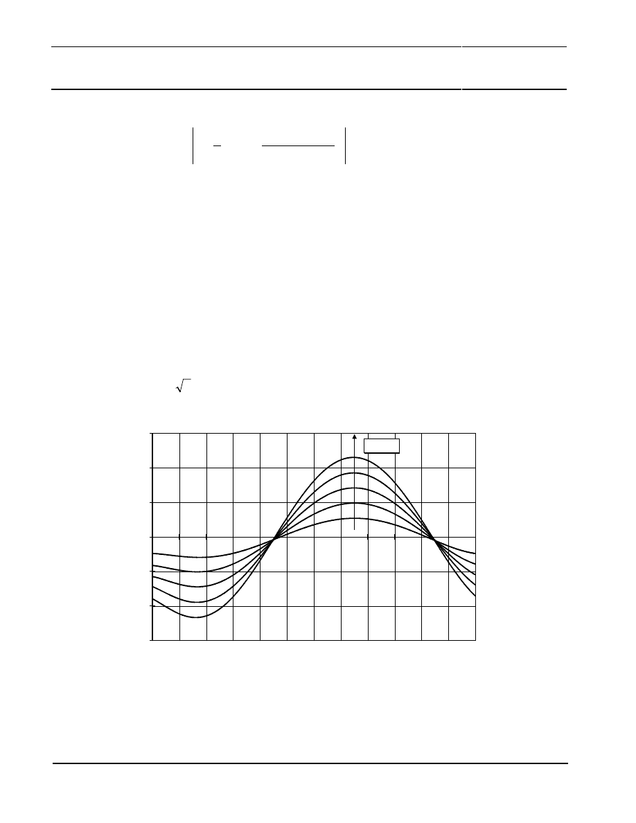
Philips Semiconductors
Contactless Angle Measurement using
KMZ41 and UZZ9001
Application
Note AN00004
41
(
)
∆
+
∆
+
−
=
∆
∆
y
Y
x
X
y
x
E
Offset
α
α
α
α
2
cos
2
sin
arctan
2
1
,
,
0
0
(13)
If both channels have the same offsets (
y
x
∆
=
∆
) , the maximum angular error is:
Amplitude
%
/
4
.
0
_
°
=
Max
Offset
E
(14)
This means that an offset of 1% referred to the amplitude (
%)
1
/
/
0
0
=
∆
=
∆
y
Y
x
X
results in a maximum
angular error of 0.4°. Please note that both signal amplitude and offset vary with temperature. Please
also note that the angular positions where these maximum errors occur are not fixed but depend on
the constellation of
∆
x to
∆
y. As these values change from part to part, locations with less errors can
not be determined in general.
If only one channel shows an offset but the other is ideal, the worst case value of Equation (14) is
reduced by the factor
2
/
1
.
-0,6
-0,4
-0,2
0
0,2
0,4
0,6
0
15
30
45
60
75
90
105
120
135
150
165
180
Angle in °
E_Of
fset
in °
Offset
Figure 27: Typical shape of the error curve caused by signal offsets
Figure 27 shows the typical shape of the measurement error over the entire angular range. The error
curve has a period of 180° what makes it distinguishable from other error shapes discussed below.
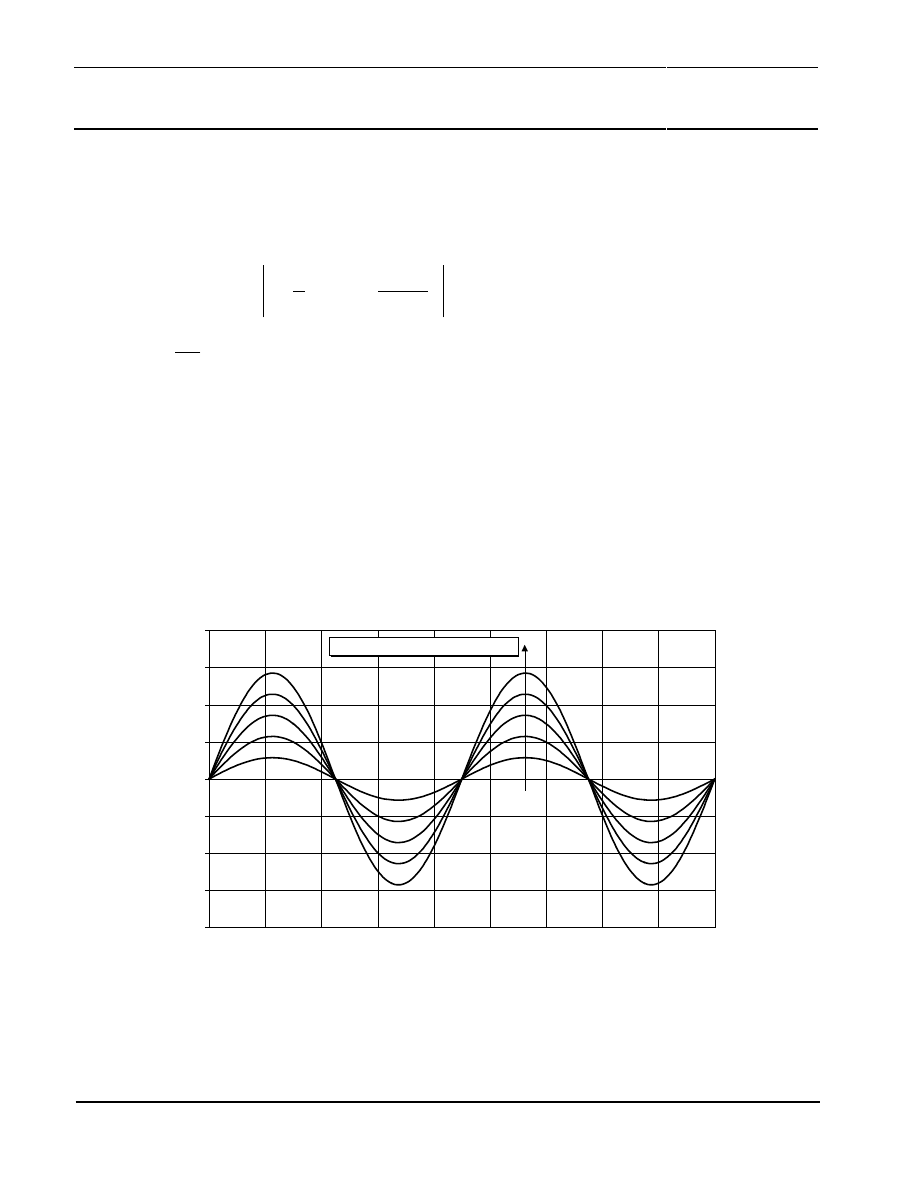
Philips Semiconductors
Contactless Angle Measurement using
KMZ41 and UZZ9001
Application
Note AN00004
42
6.1.3.2 Different Signal Amplitudes
Although processed at the same time and on the same silicon substrate, both Wheatstone bridges
may show slightly different signal amplitudes. The angular error caused by this effect is as follows:
( )
−
=
α
α
α
α
2
cos
2
sin
arctan
2
1
,
A
A
E
Amplitude
(15)
with:
0
0
Y
X
A
=
Ratio of the signal amplitudes
The maximum error due to differences of signal amplitudes is:
%
/
158
.
0
max
_
°
=
Amplitude
E
.
(16)
This means that differences between the signal amplitudes of 1% will cause a maximum angular error
of 0.158°. In contrast to the offset errors, this error function shows a period of 90°. Moreover, the
positions where maximum errors occur will not change significantly with A. Figure 28 shows the
typical shape of the output curve.
-0,20
-0,15
-0,10
-0,05
0,00
0,05
0,10
0,15
0,20
0
20
40
60
80
100
120
140
160
180
Angle in °
E_A
m
plit
ude in °
Difference in Signal Amplitudes
Figure 28: Typical shape of the error curve caused by different signal amplitudes.
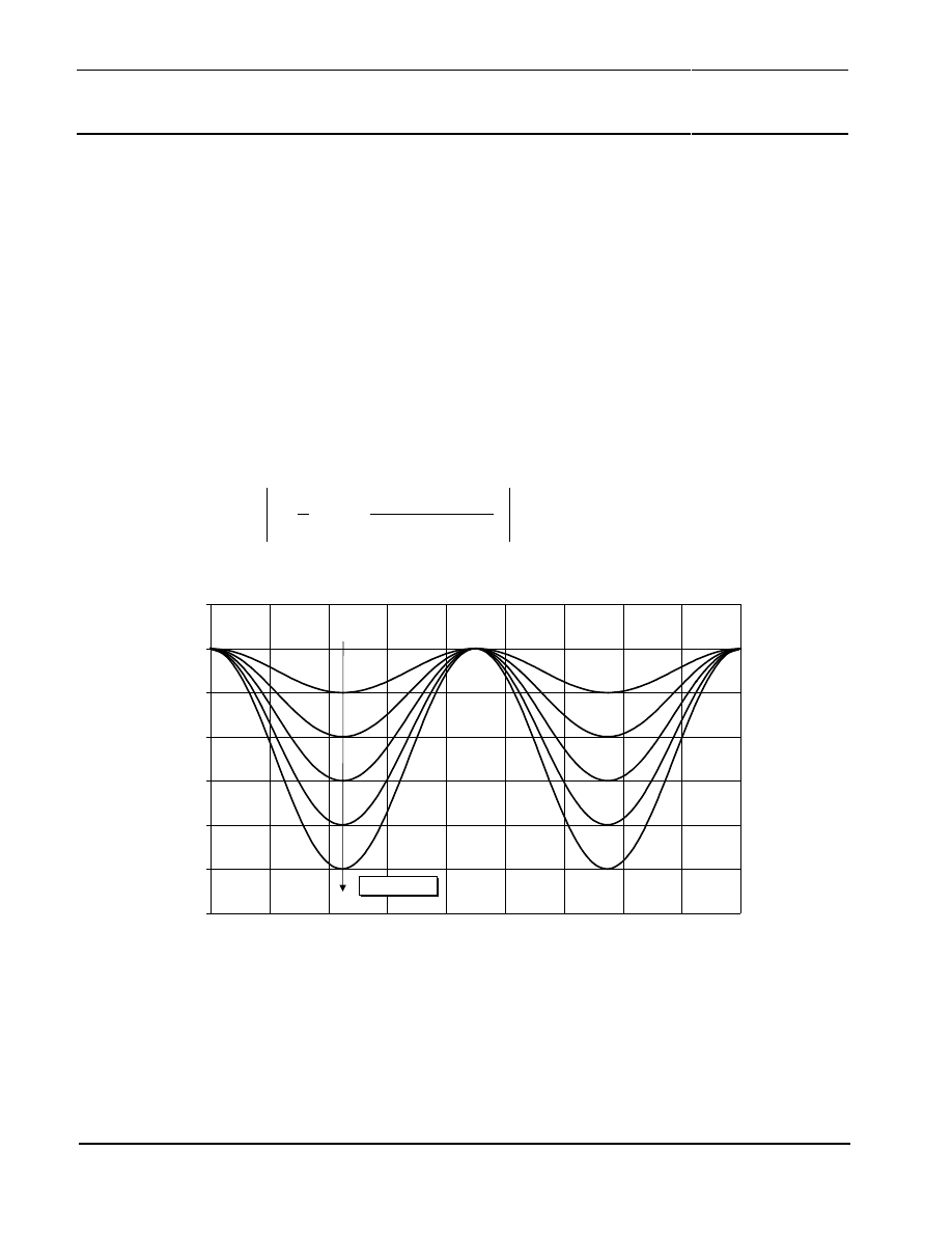
Philips Semiconductors
Contactless Angle Measurement using
KMZ41 and UZZ9001
Application
Note AN00004
43
6.1.3.3 Phase Difference between Channels
The last item to be thought of is a phase error between both channels. This means that the phase
between signal
X and Y is not exactly 90° over the entire angular range. Introducing this error into the
mathematical description of the signal gives:
( )
(
)
α
β
α ∆
+
=
2
sin
0
X
X
(17)
α
2
cos
o
Y
Y
=
(18)
Note that the phase shift is a function of the actual angle
α
and therefore may not be constant over
the entire angular range. The resulting angular error can be calculated as follows:
(
)
( )
(
)
∆
+
−
=
∆
α
α
β
α
α
β
α
2
cos
2
sin
arctan
2
1
,
Phase
E
(19)
-0,6
-0,5
-0,4
-0,3
-0,2
-0,1
0,0
0,1
0
20
40
60
80
100
120
140
160
180
Angle in °
E_
Amplitude
in °
Phase Error
Figure 29: Typical shape of an error curve caused by phase errors.
Assuming a constant phase error, the maximum measurement error that may occur is:
Shift
Phase
/
5
.
0
_
°
°
=
Max
Phase
E
(20)

Philips Semiconductors
Contactless Angle Measurement using
KMZ41 and UZZ9001
Application
Note AN00004
44
This means that a phase shift of 1° results in a maximum angular error of 0.5°. Figure 29 shows the
shape of the corresponding error function.
7.1.4
Discussion of Different Effects
When looking at the different effects discussed before, it makes sense to distinguish between errors
that can be omitted when carefully designing a system and others to which the designer has no
control.
The errors caused by insufficient magnetic fields are negligible when using a suitable magnet system.
Therefore they must only be included in the error budget, if weaker magnets should be used in order
to reduce costs. The same argumentation holds with respect to the mechanical mounting tolerances.
If accuracy is important, the magnet system can be designed to provide a larger homogeneous area,
allowing mounting tolerances without any impact on system accuracy. In turn, when a simple block
magnet is used, mounting tolerances can be limited to reasonable values of, for example,
0.1 mm eccentricity or less.
Consequently, only errors caused by offset, different signal amplitudes and phase shift between the
two channels should be taken into account. As process scatters cause these errors, it is adequate to
use a statistical calculation of the overall error for the KMZ41. This can be formulated mathematically
as given in Equation (24):
2
_
2
_
2
_
_
41
Max
Phase
Max
Amplitude
Max
Offset
Max
KMZ
E
E
E
E
+
+
=
(21)
In order to get the overall error for the measurement system the errors caused by the UZZ9001 have
to be added to this value.
6.2 Signal Conditioning IC UZZ9001
There are several blocks in the UZZ9001 that may cause errors, e.g. the ADC and the ALU. These
errors should not be discussed in detail. An analysis shows that the accuracy of the UZZ9001 is
better than 0.35° in any case. This value holds over the entire specified temperature range and at all
angular ranges provided.
°
<
45
.
0
_ Max
Signal
E
(22)
This worst case value is true for the 180° angular range of the UZZ9001. In smaller angular ranges,
however, the absolute error caused by the DAC becomes smaller because then the whole output
voltage range is matched to that smaller range. But as this does not significantly reduce the overall

Philips Semiconductors
Contactless Angle Measurement using
KMZ41 and UZZ9001
Application
Note AN00004
45
error of the UZZ9001, for simplicity, the worst case value should be used for error calculations to be
on the safe side.
Additionally, the accuracy and stability of the trimming voltage has to be taken into account. An
estimate of the remaining offset error after trimming can be determined according to the following
procedure (compare with section 5.4):
1.
Determine the maximum voltage error of the resistor divider used for offset compensation with
temperature and over lifetime according to Equation (12).
2.
Determine the achievable accuracy with the trimming equipment according to Equation (11).
3.
Add both values to get the remaining offset.
Example:
Assume that the resistor divider guarantees an accuracy better than 0.2 % VDDA with temperature
and over lifetime (compare with Table 10). This means that the maximum offset voltage due to this
effect would be less than 0.12 mV at 5V supply voltage (see Equation (12)).
Moreover, the measurement and trimming equipment may guarantee a duty cycle between 49.96%
and 50.04%. According to Equation (11), the remaining offset voltage would be less than 0.1 mV at
5V supply voltage. Consequently, the DC offset voltage caused by non-ideal trimming is:
mV
0.22
mV
1
.
0
mV
12
.
0
_
=
+
=
Trim
Offset
U
(23)
This resulting angular error
Trim
E
has to be added to the value resulting from offset drift of the KMZ41.
Consequently, the overall error budget for the UZZ9001 is:
2
2
_
_
9000
Trim
Max
Signal
Max
UZZ
E
E
E
+
=
(24)
6.3 Application Example for Error Calculation
The following example serves to demonstrate a way to calculate the minimum accuracy that can be
expected from a MR based measurement system under certain system constraints. The component
specific data are taken from the current specification of the KMZ41 and UZZ9001 (see references (1)
and (2)). As these devices are targets to continuous improvement, please refer to the latest data
sheets to get data presently valid.
The system data assumed and the component data used are as follows:

Philips Semiconductors
Contactless Angle Measurement using
KMZ41 and UZZ9001
Application
Note AN00004
46
•
Temperature range required for the system:
-40°C to 85°C
•
Temperature while trimming:
25°C
•
Maximum phase error between channels:
0.5°
•
Maximum error of amplitude synchronism (k):
0.5 %
•
Offset Drift (TCVoffset):
2
µ
V / V / K
•
Constant offset due to non-ideal trimming:
0.2 mV
•
Supply voltage:
5 V
•
Signal amplitude KMZ41:
78 mV @ 25°C
•
Temperature coefficient of peak voltage (TCVpeak):
-0.31 % / K
The temperature during trimming is 25°C and therefore lies in the middle of the required operating
temperature range. Consequently, the maximum change of temperature referred to this trimming
temperature is about 60°C.
Nevertheless the upper limit of the operating temperature range of 85°C is more critical because the
signal amplitude decreases with higher temperatures and therefore the percentage of offset to be
taken into account increases. With the given data, the maximum offset voltage at 85°C is:
mV
0.60
C
60
5V
C
V/V/
2
_
=
°
⋅
⋅
°
=
µ
Max
Offset
U
(25)
The amplitude of the signal at 85°C is 63.5 mV which is calculated using Equation (6)
(TCVpeak = -0.31 % / K). As a result, the maximum offset caused by offset drift is:
%
94
.
0
%
100
mV
5
.
63
mV
60
.
0
=
=
Max
Offset
(26)
The graph in Figure 30 shows the results of this calculation at other temperatures. For example, the
offset drift to be taken into account at 125°C would be 1.7 %. At the maximum temperature of 150°C,
2.6 % offset may occur.

Philips Semiconductors
Contactless Angle Measurement using
KMZ41 and UZZ9001
Application
Note AN00004
47
0
0,5
1
1,5
2
2,5
3
-40 -30 -20 -10
0
10
20
30
40
50
60
70
80
90
100 110 120 130 140 150
Temperature in °C
O
ff
set
in %
Figure 30: Offset drift at different maximum temperatures assuming the data defined in the text.
The maximum angular error caused by this offset drift can be calculated according to Equation (17).
An offset of 0.94% corresponds to a maximum angular error of
°
=
°
⋅
=
38
.
0
%
/
4
.
0
%
94
.
0
_ Max
Offset
E
.
(27)
In addition to offset drift, the trim error adds another portion. With the given remaining offset voltage
of 0.2 mV after trimming, the evaluation of Equation (17) and Equation (29) results in:
°
=
°
⋅
=
13
.
0
%
/
4
.
0
mV
5
63
mV
2
.
0
.
E
Trim
(28)
Similarly, the maximum phase error and the maximum amplitude error can be calculated according to
Equation (19) and Equation (23). The results are:
°
=
°
⋅
=
08
.
0
%
/
158
.
0
%
5
.
0
_ Max
Amplitude
E
(29)
°
=
°
°
⋅
°
=
25
.
0
/
5
.
0
5
.
0
_ Max
Phase
E
(30)
This gives an overall error of
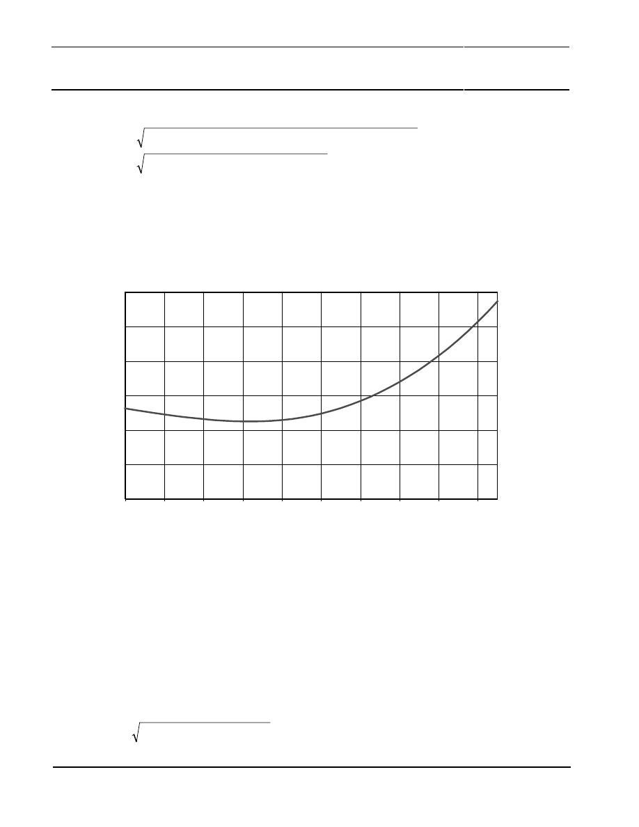
Philips Semiconductors
Contactless Angle Measurement using
KMZ41 and UZZ9001
Application
Note AN00004
48
°
=
°
+
+
+
+
=
+
+
+
+
=
59
.
0
35
.
0
08
.
0
25
.
0
13
.
0
38
.
0
2
2
2
2
2
2
_
2
_
2
_
2
2
_
Max
Signal
Max
Amplitude
Max
Phase
Trim
Max
Offset
Max
E
E
E
E
E
E
(31)
As a result, an accuracy better than 0.6° can be expected under the given constraints.
Please note that due to the input of 3-Sigma values, this result is a 3-Sigma value also and thus
typical accuracy will be significantly higher than calculated here. When using the 180° angular range,
the relative error would be less than 0.4 %.
Figure 31: Maximum absolute angular error over temperature assuming the system data given in the example described in
the text. The graph shows 3-Sigma values.
Similar calculations can be carried out for other temperature ranges. The result is shown in Figure 31.
At 150°C, for example, a maximum error of 1.2° may occur. Again, this is a 3-Sigma value and
therefore typical accuracy would be much better than calculated here.
The error
E
System
describes the angle error of the hole measuring system. Therefore, the errors
E
inhomogenoeus
and
E
Form
must be included (section 6.1.2). The overall error
E
System
can be calculated as
follows:
2
2
2
Form
omogenoeus
Inh
Max
System
E
E
E
E
+
+
=
(32)
0
0,2
0,4
0,6
0,8
1
1,2
-40
-20
0
20
40
60
80
100
120
140
Temperature in °C
Maximum Angular Error in °

Philips Semiconductors
Contactless Angle Measurement using
KMZ41 and UZZ9001
Application
Note AN00004
49
The error
E
inhomogenoeus
has very often the highest component in the error calculation. This means the
effects of inhomogeneous magnetic fields are resulting in high angle errors (see section 6.1.2).
Therefore small mounting tolerances are strongly recommend when using a simple block magnet
arrangement (see Figure 2). Lower angle errors at higher mounting tolerances are expected with
magnetic arrangements shown in section 4.4. An application specific solution must found between
system accuracy and system costs.
A measured angle error
E
System
is given in Figure 32. It shows that the angle error can be lower than
0.25° by a proper magnetic arrangement.
Figure 32: Measured angle error E
system
for a typical set-up
0
0,05
0,1
0,15
0,2
0,25
-50
0
50
100
150
Temperature in °C
a
ngl
e
e
rror
E
syst
em
in
°

Philips Semiconductors
Contactless Angle Measurement using
KMZ41 and UZZ9001
Application
Note AN00004
50
7 REFERENCES
[1] KMZ41, Tentative Specification, Philips Semiconductors, August 1998
[2] UZZ9001 Sensor Conditioning Electronics, Objective Specification, Data Sheet, File under
Discrete Semiconductors Data Book, SC17, Philips Semiconductors, 1998-08-20
[3] G. C. Giels: A 540 MHz 10-bit Polar to Cartesian Converter. IEEE Journal of Solid-States
Circuits, Vol. 26, No 11, Nov. 1991, pp. 1645-1650.
[4] E. v. d. Zwan: Low Power CMOS Sigma-Delta A/D converters for speech coding. Philips
Research, Nat. Lab. Technical Note NR. 230/95, 1995
[5] E. Hogenauer: An Economical Class of Digital Filters for Decimation and interpolation. IEEE
Trans ASSP-29, No.2, April 1981, pp. 155-162
[6] K. Dietmayer: Contactless Angle Measurement using KMZ41 and UZZ9000, Philips
Semiconductors, Application Note AN98097, 16.12.1998
Wyszukiwarka
Podobne podstrony:
appnote
APPNOTE DOC
modeling resistors appnote
KMZ41 3
IC12 97 APPNOTE 1
PDIUSBH11A APPNOTES
PDIUSBH11A KBD APPNOTES
nonlinear capacitor model appnote
więcej podobnych podstron