
Rajashekara, K., Bhat, A.K.S., Bose, B.K. “Power Electronics”
The Electrical Engineering Handbook
Ed. Richard C. Dorf
Boca Raton: CRC Press LLC, 2000

© 2000 by CRC Press LLC
30
Power Electronics
30.1 Power Semiconductor Devices
Thyristor and Triac • Gate Turn-Off Thyristor (GTO) • Reverse-
Conducting Thyristor (RCT) and Asymmetrical Silicon- Controlled
Rectifier (ASCR) • Power Transistor • Power MOSFET •
Insulated-Gate Bipolar Transistor (IGBT) • MOS Controlled
Thyristor (MCT)
AC-DC Converters • Cycloconverters • DC-to-AC
Converters • DC-DC Converters
DC Power Supplies • AC Power Supplies • Special Power Supplies
30.4 Converter Control of Machines
Converter Control of DC Machines • Converter Control of AC
Machines
30.1 Power Semiconductor Devices
Kaushik Rajashekara
The modern age of power electronics began with the introduction of thyristors in the late 1950s. Now there
are several types of power devices available for high-power and high-frequency applications. The most notable
power devices are gate turn-off thyristors, power Darlington transistors, power MOSFETs, and insulated-gate
bipolar transistors (IGBTs). Power semiconductor devices are the most important functional elements in all
power conversion applications. The power devices are mainly used as switches to convert power from one form
to another. They are used in motor control systems, uninterrupted power supplies, high-voltage dc transmission,
power supplies, induction heating, and in many other power conversion applications. A review of the basic
characteristics of these power devices is presented in this section.
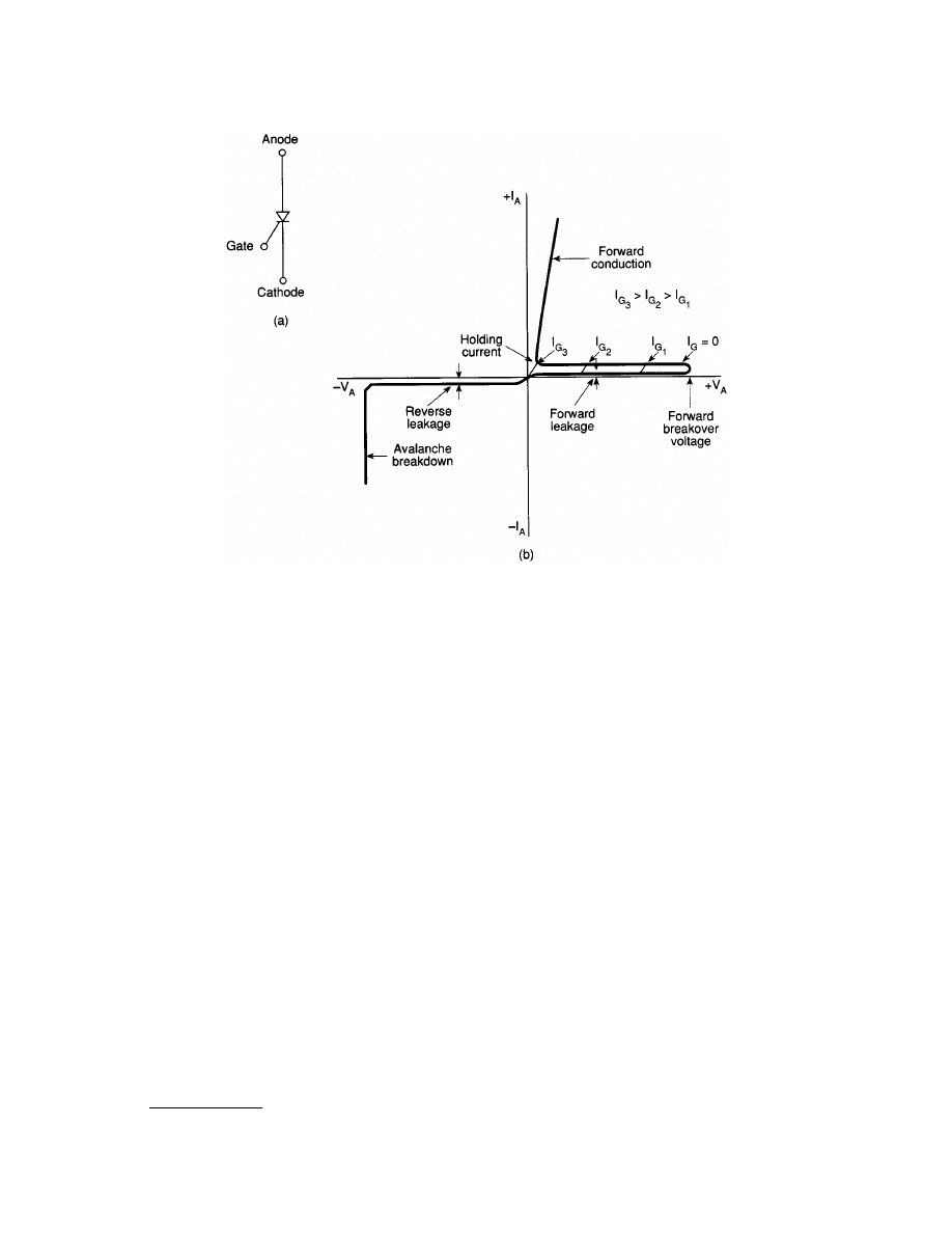
Thyristor and Triac
The thyristor, also called a silicon-controlled rectifier (SCR), is basically a four-layer three-junction
pnpn
device.
It has three terminals: anode, cathode, and gate. The device is turned on by applying a short pulse across the
gate and cathode. Once the device turns on, the gate loses its control to turn off the device. The turn-off is
achieved by applying a
across the anode and cathode. The thyristor symbol and its volt-ampere
characteristics are shown in
. There are basically two classifications of thyristors: converter grade and
inverter grade. The difference between a converter-grade and an inverter-grade thyristor is the low turn-off
time (on the order of a few microseconds) for the latter. The converter-grade thyristors are slow type and are
used in natural commutation (or phase-controlled) applications. Inverter-grade thyristors are used in forced
commutation applications such as dc-dc choppers and dc-ac inverters. The inverter-grade thyristors are turned
off by forcing the current to zero using an external commutation circuit. This requires additional commutating
components, thus resulting in additional losses in the inverter.
Kaushik Rajashekara
Delphi Energy & Engine
Management Systems
Ashoka K. S. Bhat
University of Victoria
Bimal K. Bose
University of Tennessee
© 2000 by CRC Press LLC
Thyristors are highly rugged devices in terms of transient currents,
drop in thyristors is about 1.5 to 2 V, and even at higher currents of the order of 1000 A, it seldom
exceeds 3 V. While the forward voltage determines the on-state power loss of the device at any given current,
the switching power loss becomes a dominating factor affecting the device junction temperature at high
operating frequencies. Because of this, the maximum switching frequencies possible using thyristors are limited
in comparison with other power devices considered in this section.
withstand capability and can be protected by fuses. The nonrepetitive surge current
capability for thyristors is about 10 times their rated root mean square (rms) current. They must be protected
by snubber networks for
dv/dt
and
di/dt
effects. If the specified
dv/dt
is exceeded, thyristors may start conducting
without applying a gate pulse. In dc-to-ac conversion applications it is necessary to use an antiparallel diode
of similar rating across each main thyristor. Thyristors are available up to 6000 V, 3500 A.
A triac is functionally a pair of converter-grade thyristors connected in antiparallel. The triac symbol and
volt-ampere characteristics are shown in
. Because of the integration, the triac has poor reapplied
dv
/
dt
,
poor gate current sensitivity at turn-on, and longer turn-off time. Triacs are mainly used in phase control
applications such as in ac regulators for lighting and fan control and in solid-state ac relays.
Gate Turn-Off Thyristor (GTO)
The GTO is a power switching device that can be turned on by a short pulse of gate current and turned off by
a reverse gate pulse. This reverse gate current amplitude is dependent on the anode current to be turned off.
Hence there is no need for an external commutation circuit to turn it off. Because turn-off is provided by
bypassing carriers directly to the gate circuit, its turn-off time is short, thus giving it more capability for high-
frequency operation than thyristors. The GTO symbol and turn-off characteristics are shown in
GTOs have the
I
2
t
withstand capability and hence can be protected by semiconductor fuses. For reliable
operation of GTOs, the critical aspects are proper design of the gate turn-off circuit and the snubber circuit.
FIGURE 30.1
(a) Thyristor symbol and (b) volt-ampere characteristics. (
Source:
B.K. Bose,
Modern Power Electronics:
Evaluation, Technology, and Applications,
p. 5. © 1992 IEEE.)
© 2000 by CRC Press LLC
A GTO has a poor turn-off current gain of the order of 4 to 5. For example, a 2000-A peak current GTO may
require as high as 500 A of reverse gate current. Also, a GTO has the tendency to latch at temperatures above
125
°
C. GTOs are available up to about 4500 V, 2500 A.
Reverse-Conducting Thyristor (RCT) and Asymmetrical Silicon-Controlled
Rectifier (ASCR)
Normally in inverter applications, a diode in antiparallel is connected to the thyristor for commutation/free-
wheeling purposes. In RCTs, the diode is integrated with a fast switching thyristor in a single silicon chip. Thus,
FIGURE 30.2
(a) Triac symbol and (b) volt-ampere characteristics. (
Source:
B.K. Bose,
Modern Power Electronics: Evalu-
ation, Technology, and Applications,
p. 5. © 1992 IEEE.)
FIGURE 30.3
(a) GTO symbol and (b) turn-off characteristics. (
Source:
B.K. Bose,
Modern Power Electronics: Evaluation,
Technology, and Applications,
p. 5. © 1992 IEEE.)
© 2000 by CRC Press LLC
the number of power devices could be reduced. This integration brings forth a substantial improvement of the
static and dynamic characteristics as well as its overall circuit performance.
The RCTs are designed mainly for specific applications such as traction drives. The antiparallel diode limits
the reverse voltage across the thyristor to 1 to 2 V. Also, because of the reverse recovery behavior of the diodes,
the thyristor may see very high reapplied
dv/dt
when the diode recovers from its reverse voltage. This necessitates
use of large RC
snubber networks to suppress voltage transients. As the range of application of thyristors and
diodes extends into higher frequencies, their reverse recovery charge becomes increasingly important. High
reverse recovery charge results in high power dissipation during switching.
The ASCR has a similar forward blocking capability as an inverter-grade thyristor, but it has a limited reverse
blocking (about 20–30 V) capability. It has an on-state voltage drop of about 25% less than an inverter-grade
thyristor of a similar rating. The ASCR features a fast turn-off time; thus it can work at a higher frequency
than an SCR. Since the turn-off time is down by a factor of nearly 2, the size of the commutating components
can be halved. Because of this, the switching losses will also be low.
Gate-assisted turn-off techniques are used to even further reduce the turn-off time of an ASCR. The appli-
cation of a negative voltage to the gate during turn-off helps to evacuate stored charge in the device and aids
the recovery mechanisms. This will in effect reduce the turn-off time by a factor of up to 2 over the conventional
device.
Power Transistor
Power transistors are used in applications ranging from a few to several hundred kilowatts and switching
frequencies up to about 10 kHz. Power transistors used in power conversion applications are generally
npn
type. The power transistor is turned on by supplying sufficient base current, and this base drive has to be
maintained throughout its conduction period. It is turned off by removing the base drive and making the base
voltage slightly negative (within –
V
BE
(max)
). The saturation voltage of the device is normally 0.5 to 2.5 V and
increases as the current increases. Hence the on-state losses increase more than proportionately with current.
The transistor off-state losses are much lower than the on-state losses because the leakage current of the device
is of the order of a few milliamperes. Because of relatively larger switching times, the switching loss significantly
increases with switching frequency. Power transistors can block only forward voltages. The reverse peak voltage
rating of these devices is as low as 5 to 10 V.
Power transistors do not have
I
2
t
withstand capability. In other words, they can absorb only very little energy
before breakdown. Therefore, they cannot be protected by semiconductor fuses, and thus an electronic pro-
tection method has to be used.
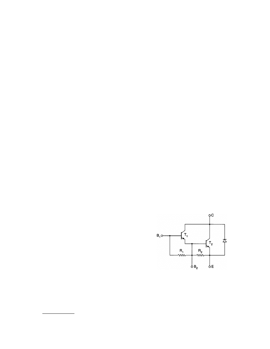
To eliminate high base current requirements, Darlington con-
figurations are commonly used. They are available in monolithic
or in isolated packages. The basic Darlington configuration is
shown schematically in
. The Darlington configuration
presents a specific advantage in that it can considerably increase
the current switched by the transistor for a given base drive. The
V
CE
(sat)
for the Darlington is generally more than that of a single
transistor of similar rating with corresponding increase in on-
state power loss. During switching, the reverse-biased collector
junction may show hot spot breakdown effects that are specified
by reverse-bias safe operating area (RBSOA) and forward bias
safe operating area (FBSOA). Modern devices with highly inter-
digited emitter base geometry force more uniform current dis-
tribution and therefore considerably improve second breakdown
effects. Normally, a well-designed switching aid network con-
strains the device operation well within the SOAs.
FIGURE 30.4
A two-stage Darlington transis-
tor with bypass diode. (Source: B.K. Bose, Mod-
ern Power Electronics: Evaluation, Technology,
and Applications, p. 6. © 1992 IEEE.)
© 2000 by CRC Press LLC
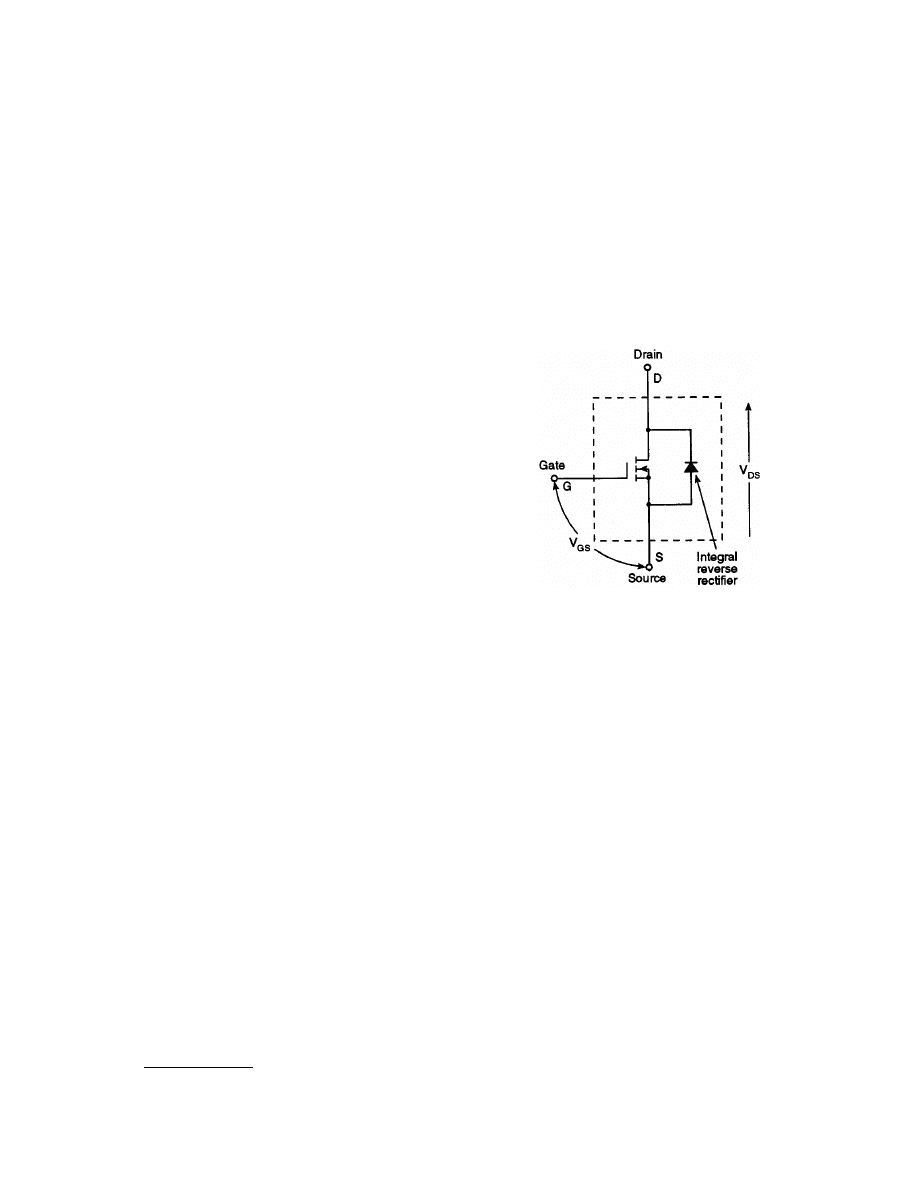
Power MOSFET
Power MOSFETs are marketed by different manufacturers with differences in internal geometry and with
different names such as MegaMOS, HEXFET, SIPMOS, and TMOS. They have unique features that make them
potentially attractive for switching applications. They are essentially voltage-driven rather than current-driven
devices, unlike bipolar transistors.
The gate of a MOSFET is isolated electrically from the source by a layer of silicon oxide. The gate draws only
a minute leakage current of the order of nanoamperes. Hence the gate drive circuit is simple and power loss
in the gate control circuit is practically negligible. Although in steady state the gate draws virtually no current,
this is not so under transient conditions. The gate-to-source and gate-to-drain capacitances have to be charged
and discharged appropriately to obtain the desired switching speed, and the drive circuit must have a sufficiently
low output impedance to supply the required charging and discharging currents. The circuit symbol of a power
MOSFET is shown in
Power MOSFETs are majority carrier devices, and there is no
minority carrier storage time. Hence they have exceptionally fast
rise and fall times. They are essentially resistive devices when
turned on, while bipolar transistors present a more or less con-
stant
V
CE
(sat)
over the normal operating range. Power dissipation
in MOSFETs is
Id
2
R
DS
(on)
, and in bipolars it is
I
C
V
CE
(sat)
. At low
currents, therefore, a power MOSFET may have a lower conduc-
tion loss than a comparable bipolar device, but at higher cur-
rents, the conduction loss will exceed that of bipolars. Also, the
R
DS
(on)
increases with temperature.
An important feature of a power MOSFET is the absence of
a secondary breakdown effect, which is present in a bipolar
transistor, and as a result, it has an extremely rugged switching
performance. In MOSFETs,
R
DS
(on)
increases with temperature,
and thus the current is automatically diverted away from the hot
spot. The drain body junction appears as an antiparallel diode
between source and drain. Thus power MOSFETs will not sup-
port voltage in the reverse direction. Although this inverse diode
is relatively fast, it is slow by comparison with the MOSFET.
Recent devices have the diode recovery time as low as 100 ns. Since MOSFETs cannot be protected by fuses,
an electronic protection technique has to be used.
With the advancement in MOS technology, ruggedized MOSFETs are replacing the conventional MOSFETs.
The need to ruggedize power MOSFETs is related to device reliability. If a MOSFET is operating within its
specification range at all times, its chances for failing catastrophically are minimal. However, if its absolute
maximum rating is exceeded, failure probability increases dramatically. Under actual operating conditions, a
MOSFET may be subjected to transients — either externally from the power bus supplying the circuit or from
the circuit itself due, for example, to inductive kicks going beyond the absolute maximum ratings. Such
conditions are likely in almost every application, and in most cases are beyond a designer’s control. Rugged
devices are made to be more tolerant for over-voltage transients. Ruggedness is the ability of a MOSFET to
operate in an environment of dynamic electrical stresses, without activating any of the parasitic bipolar junction
transistors. The rugged device can withstand higher levels of diode recovery
dv/dt
and static
dv/dt.
Insulated-Gate Bipolar Transistor (IGBT)
The IGBT has the high input impedance and high-speed characteristics of a MOSFET with the conductivity
characteristic (low saturation voltage) of a bipolar transistor. The IGBT is turned on by applying a positive
voltage between the gate and emitter and, as in the MOSFET, it is turned off by making the gate signal zero or
slightly negative. The IGBT has a much lower voltage drop than a MOSFET of similar ratings. The structure
of an IGBT is more like a thyristor and MOSFET. For a given IGBT, there is a critical value of collector current
FIGURE 30.5
Power MOSFET circuit symbol.
(Source: B.K. Bose, Modern Power Electronics:
Evaluation, Technology, and Applications, p. 7. ©
1992 IEEE.)
© 2000 by CRC Press LLC
that will cause a large enough voltage drop to activate the thyristor. Hence, the device manufacturer specifies
the peak allowable collector current that can flow without latch-up occurring. There is also a corresponding
gate source voltage that permits this current to flow that should not be exceeded.
Like the power MOSFET, the IGBT does not exhibit the secondary breakdown phenomenon common to
bipolar transistors. However, care should be taken not to exceed the maximum power dissipation and specified
maximum junction temperature of the device under all conditions for guaranteed reliable operation. The on-
state voltage of the IGBT is heavily dependent on the gate voltage. To obtain a low on-state voltage, a sufficiently
high gate voltage must be applied.
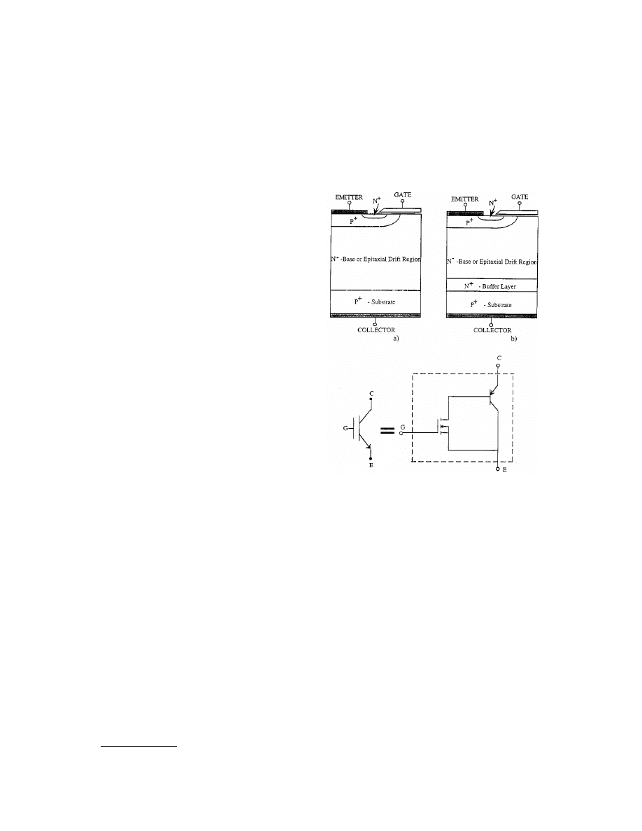
In general, IGBTs can be classified as punch-
through (PT) and nonpunch-through (NPT) struc-
tures, as shown in
. In the PT IGBT, an N
+
buffer layer is normally introduced between the P
+
substrate and the N
–
epitaxial layer, so that the whole
N
–
drift region is depleted when the device is blocking
the off-state voltage, and the electrical field shape
inside the N
–
drift region is close to a rectangular
shape. Because a shorter N
–
region can be used in the
punch-through IGBT, a better trade-off between the
forward voltage drop and turn-off time can be
achieved. PT IGBTs are available up to about 1200 V.
High voltage IGBTs are realized through non-
punch-through process. The devices are built on a N
–
wafer substrate which serves as the N
–
base drift
region. Experimental NPT IGBTs of up to about 4 KV
have been reported in the literature. NPT IGBTs are
more robust than PT IGBTs particularly under short
circuit conditions. But NPT IGBTs have a higher for-
ward voltage drop than the PT IGBTs.
The PT IGBTs cannot be as easily paralleled as
MOSFETs. The factors that inhibit current sharing of
parallel-connected IGBTs are (1) on-state current
unbalance, caused by V
CE
(sat) distribution and main
circuit wiring resistance distribution, and (2) current
unbalance at turn-on and turn-off, caused by the
switching time difference of the parallel connected devices and circuit wiring inductance distribution. The NPT
IGBTs can be paralleled because of their positive temperature coefficient property.
MOS-Controlled Thyristor (MCT)
The MCT is a new type of power semiconductor device that combines the capabilities of thyristor voltage and
current with MOS gated turn-on and turn-off. It is a high power, high frequency, low conduction drop and a
rugged device, which is more likely to be used in the future for medium and high power applications. A cross
sectional structure of a p-type MCT with its circuit schematic is shown in
. The MCT has a thyristor
type structure with three junctions and PNPN layers between the anode and cathode. In a practical MCT, about
100,000 cells similar to the one shown are paralleled to achieve the desired current rating. MCT is turned on
by a negative voltage pulse at the gate with respect to the anode, and is turned off by a positive voltage pulse.
The MCT was announced by the General Electric R & D Center on November 30, 1988. Harris Semiconductor
Corporation has developed two generations of p-MCTs. Gen-1 p-MCTs are available at 65 A/1000 V and 75A/600
V with peak controllable current of 120 A. Gen-2 p-MCTs are being developed at similar current and voltage
ratings, with much improved turn-on capability and switching speed. The reason for developing p-MCT is the
fact that the current density that can be turned off is 2 or 3 times higher than that of an n-MCT; but n-MCTs
are the ones needed for many practical applications. Harris Semiconductor Corporation is in the process of
developing n-MCTs, which are expected to be commercially available during the next one to two years.
FIGURE 30.6
Nonpunch-through IGBT, (b) Punch-
through IGBT, (c) IGBT equivalent circuit.
© 2000 by CRC Press LLC
The advantage of an MCT over-IGBT is its low forward voltage drop. N-type MCTs will be expected to have a
similar forward voltage drop, but with an improved reverse bias safe operating area and switching speed. MCTs
have relatively low switching times and storage time. The MCT is capable of high current densities and blocking
voltages in both directions. Since the power gain of an MCT is extremely high, it could be driven directly from
logic gates. An MCT has high
di/dt
(of the order of 2500 A/
m
s) and high
dv/dt
(of the order of 20,000 V/
m
s) capability.
The MCT, because of its superior characteristics, shows a tremendous possibility for applications such as
motor drives, uninterrupted power supplies, static VAR compensators, and high power active power line
conditioners.
The current and future power semiconductor devices developmental direction is shown in
. High
temperature operation capability and low forward voltage drop operation can be obtained if silicon is replaced
by silicon carbide material for producing power devices. The silicon carbide has a higher band gap than silicon.
Hence higher breakdown voltage devices could be developed. Silicon carbide devices have excellent switching
characteristics and stable blocking voltages at higher temperatures. But the silicon carbide devices are still in
the very early stages of development.
Defining Terms
di/dt limit:
Maximum allowed rate of change of current through a device. If this limit is exceeded, the device
may not be guaranteed to work reliably.
dv/dt:
Rate of change of voltage withstand capability without spurious turn-on of the device.
Forward voltage:
The voltage across the device when the anode is positive with respect to the cathode.
I
2
t:
Represents available thermal energy resulting from current flow.
Reverse voltage:
The voltage across the device when the anode is negative with respect to the cathode.
Related Topic
5.1 Diodes and Rectifiers
References
B.K. Bose,
Modern Power Electronics: Evaluation, Technology, and Applications,
New York: IEEE Press, 1992.
Harris Semiconductor,
User’s Guide of MOS Controlled Thyristor.
FIGURE 30.8
Current and future pwer semiconductor
devices development direction (
Source:
A.Q. Huang,
Recent Developments of Power Semiconductor Devices,
VPEC Seminar Proceedings, pp. 1–9. With permission.)
FIGURE 30.7
(
Source:
Harris Semiconductor,
User’s
Guide of MOS Controlled Thyristor,
With permission.)

© 2000 by CRC Press LLC
A.Q. Huang,
Recent Developments of Power Semiconductor Devices,
VPEC Seminar Proceedings, pp. 1–9, Sep-
tember 1995.
N. Mohan and T. Undeland,
Power Electronics: Converters, Applications, and Design,
New York: John Wiley &
Sons, 1995.
J. Wojslawowicz, “Ruggedized transistors emerging as power MOSFET standard-bearers,”
Power Technics Mag-
azine,
pp. 29–32, January 1988.
Further Information
B.M. Bird and K.G. King,
An Introduction to Power Electronics,
New York: Wiley-Interscience, 1984.
R. Sittig and P. Roggwiller,
Semiconductor Devices for Power Conditioning,
New York: Plenum, 1982.
V.A.K. Temple, “Advances in MOS controlled thyristor technology and capability,”
Power Conversion
, pp.
544–554, Oct. 1989.
B.W. Williams,
Power Electronics, Devices, Drivers and Applications,
New York: John Wiley, 1987.
30.2 Power Conversion
Kaushik Rajashekara
Power conversion deals with the process of converting electric power from one form to another. The power
electronic apparatuses performing the power conversion are called
power converters.
Because they contain no
moving parts, they are often referred to as
static
power converters. The power conversion is achieved using
power semiconductor devices, which are used as switches. The power devices used are SCRs (silicon controlled
rectifiers, or thyristors), triacs, power transistors, power MOSFETs, insulated gate bipolar transistors (IGBTs),
and MCTs (MOS-controlled thyristors). The power converters are generally classified as:
1. ac-dc converters (phase-controlled converters)
2. direct ac-ac converters (cycloconverters)
3. dc-ac converters (inverters)
4. dc-dc converters (choppers, buck and boost converters)
AC-DC Converters
The basic function of a
is to convert an alternating voltage of variable amplitude
and frequency to a variable dc voltage. The power devices used for this application are generally
s. The
average value of the output voltage is controlled by varying the conduction time of the SCRs. The turn-on of
the SCR is achieved by providing a gate pulse when it is forward-biased. The turn-off is achieved by the
of current from one device to another at the instant the incoming ac voltage has a higher
instantaneous potential than that of the outgoing wave. Thus there is a natural tendency for current to be
commutated from the outgoing to the incoming SCR, without the aid of any external commutation circuitry.
This commutation process is often referred to as
natural commutation.
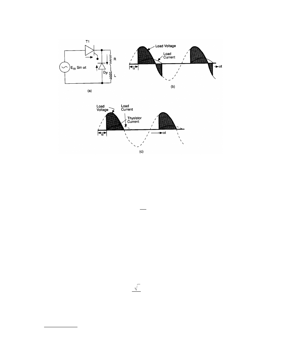
A single-phase half-wave converter is shown in
. When the SCR is turned on at an angle
a
, full
supply voltage (neglecting the SCR drop) is applied to the load. For a purely resistive load, during the positive
half cycle, the output voltage waveform follows the input ac voltage waveform. During the negative half cycle,
the SCR is turned off. In the case of inductive load, the energy stored in the inductance causes the current to
flow in the load circuit even after the reversal of the supply voltage, as shown in Fig. 30.9(b). If there is no
freewheeling diode
D
F
, the load current is discontinuous. A freewheeling diode is connected across the load to
turn off the SCR as soon as the input voltage polarity reverses, as shown in Fig. 30.9(c). When the SCR is off,
the load current will freewheel through the diode. The power flows from the input to the load only when the
SCR is conducting. If there is no freewheeling diode, during the negative portion of the supply voltage, SCR
returns the energy stored in the load inductance to the supply. The freewheeling diode improves the input
power factor.
© 2000 by CRC Press LLC
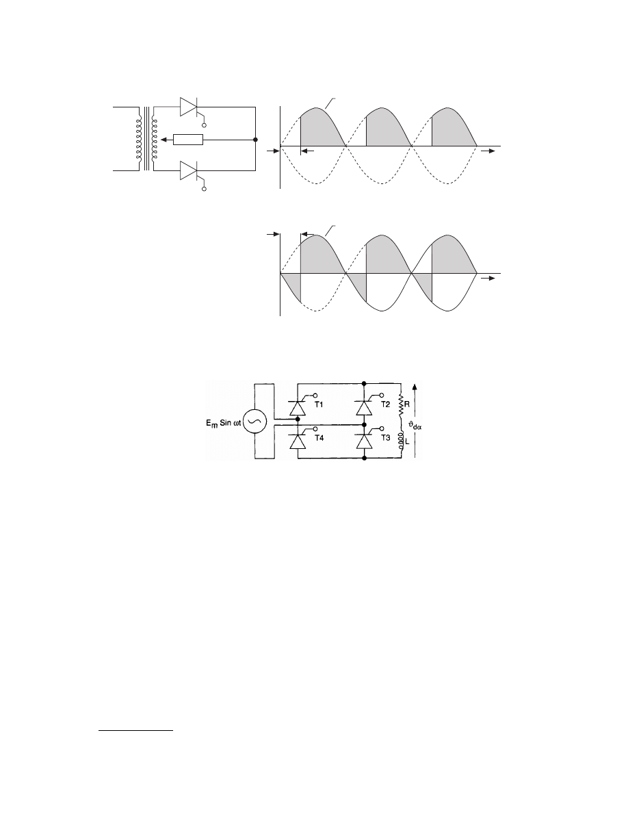
The controlled full-wave dc output may be obtained by using either a center tap transformer (
) or
by bridge configuration (
). The bridge configuration is often used when a transformer is undesirable
and the magnitude of the supply voltage properly meets the load voltage requirements. The average output
voltage of a single-phase full-wave converter for continuous current conduction is given by
where
E
m
is the peak value of the input voltage and
a
is the firing angle. The output voltage of a single-phase
bridge circuit is the same as that shown in Fig. 30.10. Various configurations of the single-phase bridge circuit
can be obtained if, instead of four SCRs, two diodes and two SCRs are used, with or without freewheeling diodes.
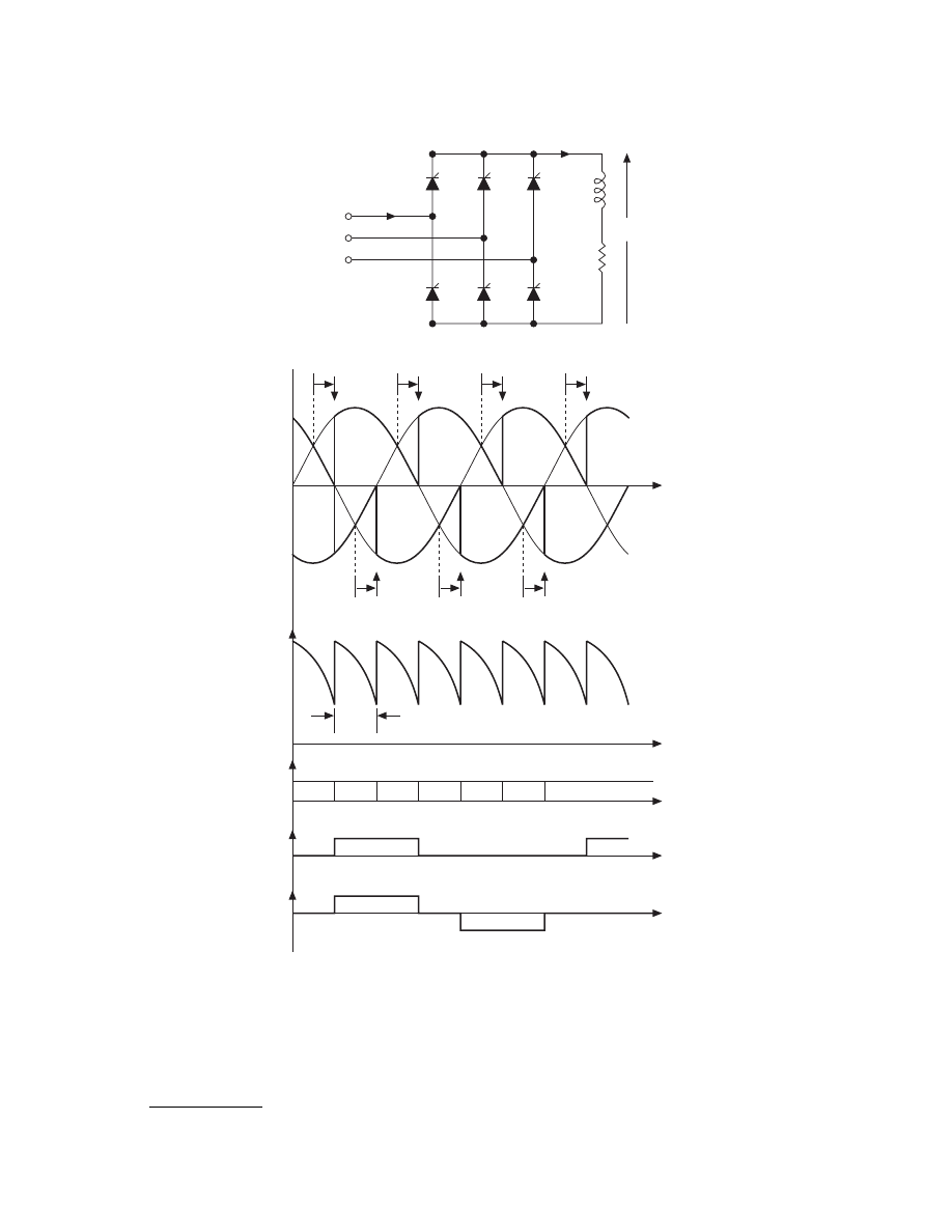
A three-phase full-wave converter consisting of six thyristor switches is shown in
. This is the
most commonly used three-phase bridge configuration. Thyristors
T
1
, T
3
, and T
5
are turned on during the
positive half cycle of the voltages of the phases to which they are connected, and thyristors T
2
, T
4
, and T
6
are
turned on during the negative half cycle of the phase voltages. The reference for the angle in each cycle is at
the crossing points of the phase voltages. The ideal output voltage, output current, and input current waveforms
are shown in
. The output dc voltage is controlled by varying the firing angle
a. The average output
voltage under continuous current conduction operation is given by
where E
m
is the peak value of the phase voltage. At
a = 90°, the output voltage is zero. For 0 < a < 90°, v
o
is
positive and power flows from ac supply to the load. For 90
° < a < 180°, v
o
is negative and the converter
operates in the inversion mode. If the load is a dc motor, the power can be transferred from the motor to the
ac supply, a process known as regeneration.
FIGURE 30.9
Single-phase half-wave converter with freewheeling diode. (a) Circuit diagram; (b) waveform for inductive
load with no freewheeling diode; (c) waveform with freewheeling diode.
v
E
d
m
a
p
a
= 2 cos
v
E
o
m
=
3 3
p
a
cos
© 2000 by CRC Press LLC
In Fig. 30.12(a), the top or bottom thyristors could be replaced by diodes. The resulting topology is called
a thyristor semiconverter. With this configuration, the input power factor is improved, but the regeneration is
not possible.
Cycloconverters
Cycloconverters are direct ac-to-ac frequency changers. The term direct conversion means that the energy does
not appear in any form other than the ac input or ac output. The output frequency is lower than the input
frequency and is generally an integral multiple of the input frequency. A cycloconverter permits energy to be
fed back into the utility network without any additional measures. Also, the phase sequence of the output
voltage can be easily reversed by the control system. Cycloconverters have found applications in aircraft systems
and industrial drives. These cycloconverters are suitable for synchronous and induction motor control. The
operation of the cycloconverter is illustrated in Section 30.4 of this chapter.
DC-to-AC Converters
The dc-to-ac converters are generally called inverters. The ac supply is first converted to dc, which is then
converted to a variable-voltage and variable-frequency power supply. This generally consists of a three-phase
bridge connected to the ac power source, a dc link with a filter, and the three-phase inverter bridge connected
FIGURE 30.10
Single-phase full-wave converter with transformer.
FIGURE 30.11
Single-phase bridge converter.
(a) For Resistive Load
a
Load Voltage & Current
wt
(b) For Resistive-Inductive Load (with continuous current conduction)
a
Load Voltage
wt
T1
Load
Sin
wt
E
m
T2
© 2000 by CRC Press LLC
to the load. In the case of battery-operated systems, there is no intermediate dc link. Inverters can be classified
as voltage source inverters (VSIs) and current source inverters (CSIs). A voltage source inverter is fed by a stiff
dc voltage, whereas a current source inverter is fed by a stiff current source. A voltage source can be converted
to a current source by connecting a series inductance and then varying the voltage to obtain the desired current.
FIGURE 30.12
(a) Three-phase thyristor full bridge configuration; (b) output voltage and current waveforms.
T1
i
A
v
AN
v
BN
v
CN
T3
T5
T4
T6
T2
R
L
+
i
0
v
O
(a)
T4
T6
T2
T1
T3
T5
a
a
a
a
v
AN
v
BN
v
CN
a
a
a
T6
wt
v
AB
v
O
v
AC
v
BC
60
°
i
O
i
TI
i
A
T1 T6 T1 T2
T1
T1
T1
T4
wt
wt
wt
wt
(b)
© 2000 by CRC Press LLC
A VSI can also be operated in current-controlled mode, and similarly a CSI can also be operated in the voltage-
control mode. The inverters are used in variable frequency ac motor drives, uninterrupted power supplies,
induction heating, static VAR compensators, etc.
Voltage Source Inverter
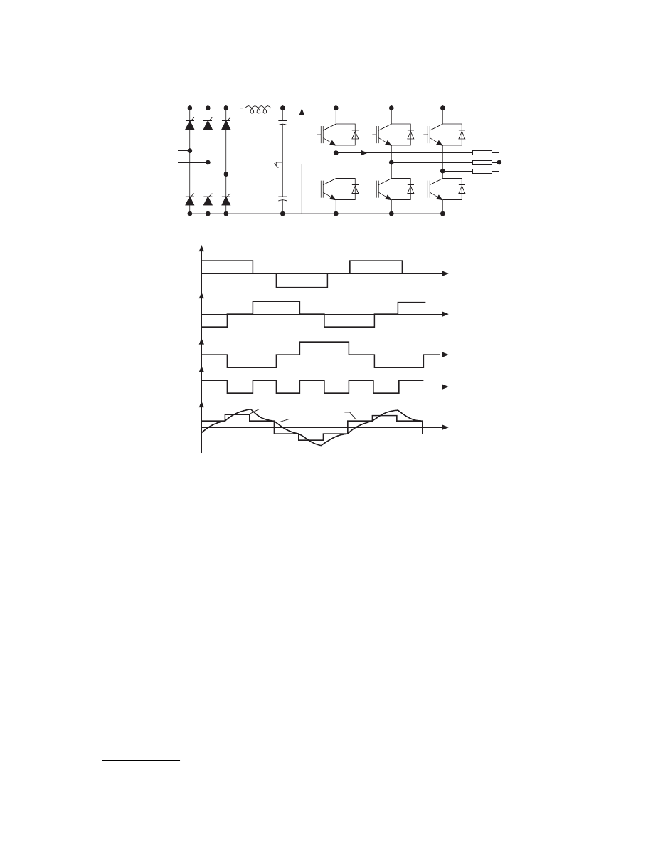
A three-phase voltage source inverter configuration is shown in
. The VSIs are controlled either
in square-wave mode or in pulsewidth-modulated (PWM) mode. In square-wave mode, the frequency of the
output voltage is controlled within the inverter, the devices being used to switch the output circuit between
the plus and minus bus. Each device conducts for 180 degrees, and each of the outputs is displaced 120 degrees
to generate a six-step waveform, as shown in
. The amplitude of the output voltage is controlled
by varying the dc link voltage. This is done by varying the firing angle of the thyristors of the three-phase bridge
converter at the input. The square-wave-type VSI is not suitable if the dc source is a battery. The six-step output
voltage is rich in harmonics and thus needs heavy filtering.
In PWM inverters, the output voltage and frequency are controlled within the inverter by varying the width
of the output pulses. Hence at the front end, instead of a phase-controlled thyristor converter, a diode bridge
rectifier can be used. A very popular method of controlling the voltage and frequency is by sinusoidal pulsewidth
modulation. In this method, a high-frequency triangle carrier wave is compared with a three-phase sinusoidal
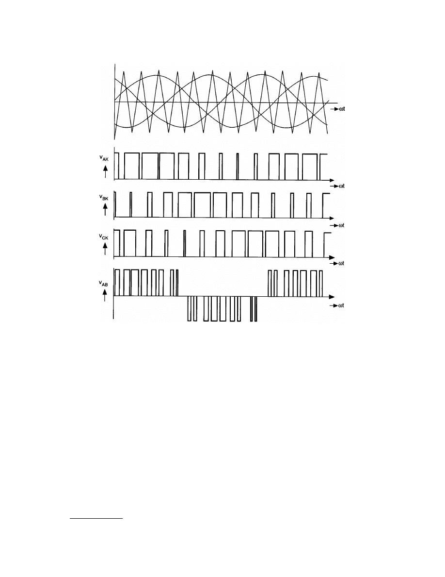
waveform, as shown in
. The power devices in each phase are switched on at the intersection of sine
FIGURE 30.13
(a) Three-phase converter and voltage source inverter configuration; (b) three-phase square-wave inverter
waveforms.
3 - Phase
+
V
T1
i
A
O
–
A
T4
T3
B
T6
T5
C
T2
N
Inverter
K
(a)
L
F
v
AB
v
BC
v
CA
v
NO
v
AN
i
A
(b)
wt
wt
wt
wt
wt
V/3
V/6
-V
V
V
-V
-V
V
-V
2/3 V
v
AN
i
A
© 2000 by CRC Press LLC
and triangle waves. The amplitude and frequency of the output voltage are varied, respectively, by varying the
amplitude and frequency of the reference sine waves. The ratio of the amplitude of the sine wave to the amplitude
of the carrier wave is called the modulation index.
The harmonic components in a PWM wave are easily filtered because they are shifted to a higher-frequency
region. It is desirable to have a high ratio of carrier frequency to fundamental frequency to reduce the harmonics
of lower-frequency components. There are several other PWM techniques mentioned in the literature. The
most notable ones are selected harmonic elimination, hysteresis controller, and space vector PWM technique.
In inverters, if SCRs are used as power switching devices, an external forced commutation circuit has to be
used to turn off the devices. Now, with the availability of IGBTs above 1000-A, 1000-V ratings, they are being
used in applications up to 300-kW motor drives. Above this power rating, GTOs are generally used. Power
Darlington transistors, which are available up to 800 A, 1200 V, could also be used for inverter applications.
Current Source Inverter
Contrary to the voltage source inverter where the voltage of the dc link is imposed on the motor windings, in
the current source inverter the current is imposed into the motor. Here the amplitude and phase angle of the
motor voltage depend on the load conditions of the motor. The current source inverter is described in detail
in Section 30.4.
FIGURE 30.14
Three-phase sinusoidal PWM inverter waveforms.
© 2000 by CRC Press LLC
Resonant-Link Inverters
The use of resonant switching techniques can be applied to inverter topologies to reduce the switching losses
in the power devices. They also permit high switching frequency operation to reduce the size of the magnetic
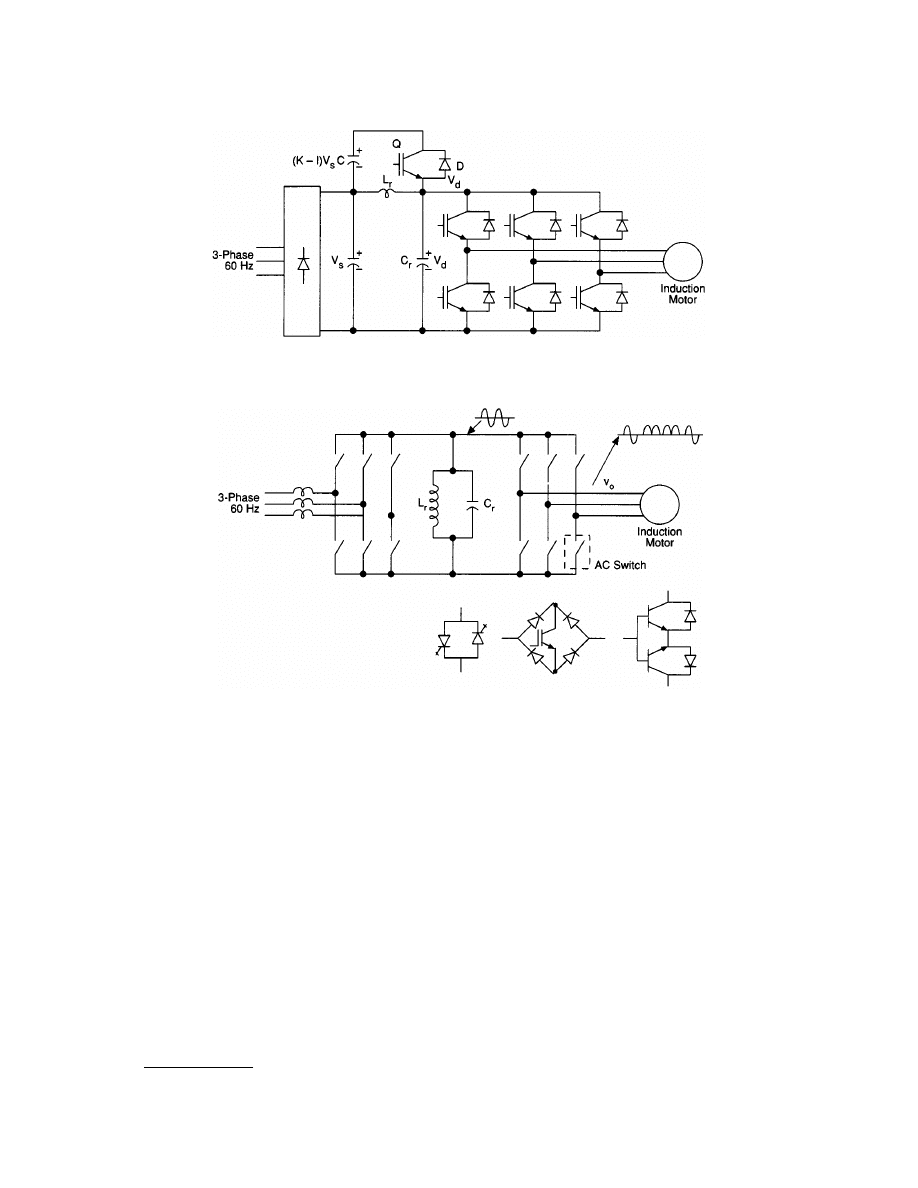
components in the inverter unit. In the resonant dc-link inverter shown in
, a resonant circuit is
added at the inverter input to convert a fixed dc voltage to a pulsating dc voltage. This resonant circuit enables
the devices to be turned on and turned off during the zero voltage interval. Zero voltage or zero current
switching is often termed soft switching. Under soft switching, the switching losses in the power devices are
almost eliminated. The electromagnetic interference (EMI) problem is less severe because resonant voltage
pulses have lower dv/dt compared to those of hard-switched PWM inverters. Also, the machine insulation is
less stretched because of lower dv/dt resonant voltage pulses. In Fig. 30.15, all the inverter devices are turned
on simultaneously to initiate a resonant cycle. The commutation from one device to another is initiated at the
zero dc-link voltage. The inverter output voltage is formed by the integral numbers of quasi-sinusoidal pulses.
The circuit consisting of devices Q, D, and the capacitor C acts as an active clamp to limit the dc voltage to
about 1.4 times the diode rectifier voltage V
s
.
There are several other topologies of resonant link inverters mentioned in the literature. There are also
resonant link ac-ac converters based on bidirectional ac switches, as shown in
. These resonant link
converters find applications in ac machine control and uninterrupted power supplies, induction heating, etc.
The resonant link inverter technology is still in the development stage for industrial applications.
FIGURE 30.15
Resonant dc-link inverter system with active voltage clamping.
FIGURE 30.16
Resonant ac-link converter system showing configuration of ac switches.
© 2000 by CRC Press LLC
DC-DC Converters
DC-dc converters are used to convert unregulated dc voltage to regulated or variable dc voltage at the output.
They are widely used in switch-mode dc power supplies and in dc motor drive applications. In dc motor control
applications, they are called chopper-controlled drives. The input voltage source is usually a battery or derived
from an ac power supply using a diode bridge rectifier. These converters are generally either hard-switched
PWM types or soft-switched resonant-link types. There are several dc-dc converter topologies, the most
common ones being buck converter, boost converter, and buck-boost converter, shown in
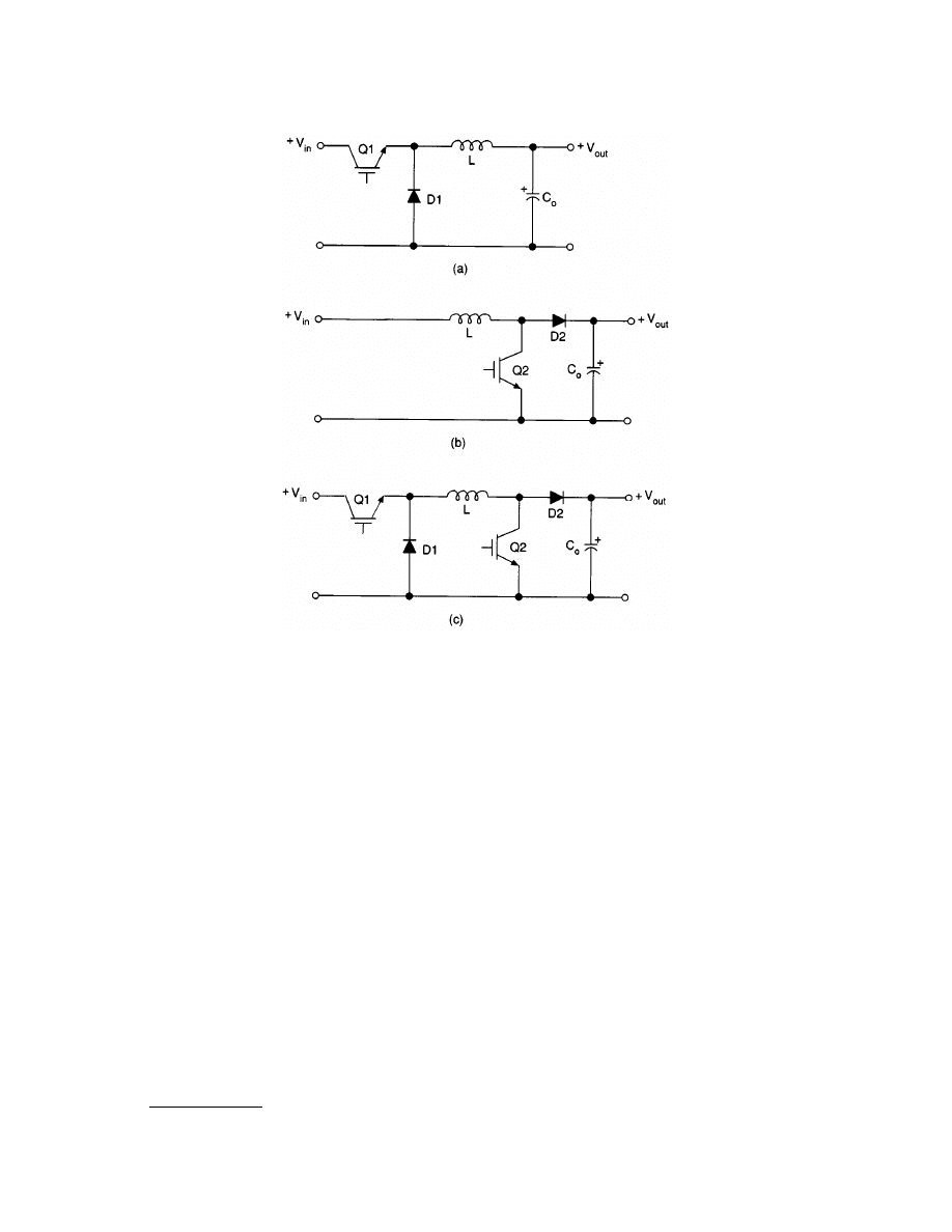
Buck Converter
A buck converter is also called a step-down converter. Its principle of operation is illustrated by referring to
Fig. 30.17(a). The IGBT acts as a high-frequency switch. The IGBT is repetitively closed for a time t
on
and
opened for a time t
off
. During t
on
, the supply terminals are connected to the load, and power flows from supply
to the load. During t
off
, load current flows through the freewheeling diode D
1
, and the load voltage is ideally
zero. The average output voltage is given by
V
out
= DV
in
where D is the
of the switch and is given by D = t
on
/T, where T is the time for one period. 1/T is
the switching frequency of the power device IGBT.
Boost Converter
A boost converter is also called a step-up converter. Its principle of operation is illustrated by referring to
Fig. 30.17(b). This converter is used to produce higher voltage at the load than the supply voltage. When the
FIGURE 30.17
DC-DC converter configurations: (a) buck converter; (b) boost converter; (c) buck-boost converter.
© 2000 by CRC Press LLC
power switch is on, the inductor is connected to the dc source and the energy from the supply is stored in it.
When the device is off, the inductor current is forced to flow through the diode and the load. The induced
voltage across the inductor is negative. The inductor adds to the source voltage to force the inductor current
into the load. The output voltage is given by
Thus for variation of D in the range 0 < D < 1, the load voltage V
out
will vary in the range V
in
< V
out
<
`.
Buck-Boost Converter
A buck-boost converter can be obtained by the cascade connection of the buck and the boost converter. The
steady-state output voltage V
out
is given by
This allows the output voltage to be higher or lower than the input voltage, based on the duty cycle D. A typical
buck-boost converter topology is shown in Fig. 30.17(c). When the power device is turned on, the input provides
energy to the inductor and the diode is reverse biased. When the device is turned off, the energy stored in the
inductor is transferred to the output. No energy is supplied by the input during this interval. In dc power
supplies, the output capacitor is assumed to be very large, which results in a constant output voltage. In dc
drive systems, the chopper is operated in step-down mode during motoring and in step-up mode during
regeneration operation.
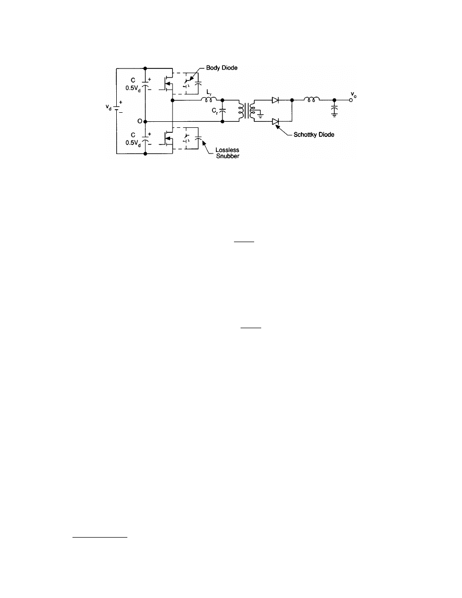
Resonant-Link DC-DC Converters
The use of resonant converter topologies would help to reduce the switching losses in dc-dc converters and
enable the operation at switching frequencies in the megahertz range. By operating at high frequencies, the size
of the power supplies could be reduced. There are several types of resonant converter topologies. The most
popular configuration is shown in
. The dc power is converted to high-frequency alternating power
using the MOSFET half-bridge inverter. The resonant capacitor voltage is transformer-coupled, rectified using
the two Schottky diodes, and then filtered to get output dc voltage. The output voltage is regulated by control
of the inverter switching frequency.
Instead of parallel loading as in Fig. 30.18, the resonant circuit can be series-loaded; that is, the transformer
in the output circuit can be placed in series with the tuned circuit. The series resonant circuit provides the
short-circuit limiting feature.
FIGURE 30.18
Resonant-link dc-dc converter.
V
V
D
out
in
=
1 –
V
V
D
D
out in
=
1 –

© 2000 by CRC Press LLC
There are other forms of resonant converter topologies mentioned in the literature such as quasi-resonant
converters and multiresonant converters. These resonant converter topologies find applications in high-density
power supplies.
Defining Terms
Commutation:
Process of transferring the current from one power device to another.
Duty cycle:
Ratio of the on-time of a switch to the switching period.
Full-wave control:
Both the positive and negative half cycle of the waveforms are controlled.
IGBT:
Insulated-gate bipolar transistor.
Phase-controlled converter:
Converter in which the power devices are turned off at the natural crossing of
zero voltage in ac to dc conversion applications.
SCR:
Silicon-controlled rectifier.
Related Topics
33.2 Heat Transfer Fundamentals • 61.3 High-Voltage Direct-Current Transmission
References
B.K. Bose, Modern Power Electronics, New York: IEEE Press, 1992.
Motorola, Linear/Switchmode Voltage Regulator Handbook, 1989.
K.S. Rajashekara, H. Le-Huy, et al., “Resonant DC Link Inverter-Fed AC Machines Control,” IEEE Power
Electronics Specialists Conference, 1987, pp. 491–496.
P.C. Sen, Thyristor DC Drives, New York: John Wiley, 1981.
G. Venkataramanan and D. Divan, “Pulse Width Modulation with Resonant DC Link Converters,” IEEE IAS
Annual Meeting, 1990, pp. 984–990.
Further Information
B.K. Bose, Power Electronics & AC Drives, Englewood Cliffs, N.J.: Prentice-Hall, 1986.
R. Hoft, Semiconductor Power Electronics, New York: Van Nostrand Reinhold, 1986.
B.R. Pelly, Thyristor Phase Controlled Converters and Cycloconverters, New York: Wiley-Interscience, 1971.
A.I. Pressman, Switching and Linear Power Supply, Power Converter Design, Carmel, Ind.: Hayden Book Com-
pany, 1977.
M.H. Rashid, Power Electronics, Circuits, Devices and Applications, Englewood Cliffs, N.J.: Prentice-Hall, 1988.
30.3 Power Supplies
Ashoka K. S. Bhat
Power supplies are used in many industrial and aerospace applications and also in consumer products. Some
of the requirements of power supplies are small size, light weight, low cost, and high power conversion efficiency.
In addition to these, some power supplies require the following: electrical isolation between the source and
load, low harmonic distortion for the input and output waveforms, and high power factor (PF) if the source
is ac voltage. Some special power supplies require controlled direction of power flow.
Basically two types of power supplies are required: dc power supplies and ac power supplies. The output of
dc power supplies is regulated or controllable dc, whereas the output for ac power supplies is ac. The input to
these power supplies can be ac or dc.

© 2000 by CRC Press LLC
DC Power Supplies
If an ac source is used, then ac-to-dc
explained in Section 30.2 can be used. In these converters,
electrical isolation can only be provided by bulky line frequency transformers. The ac source can be rectified
with a diode rectifier to get an uncontrolled dc, and then a dc-to-dc converter can be used to get a controlled
dc output. Electrical isolation between the input source and the output load can be provided in the dc-to-dc
converter using a high-frequency (HF) transformer. Such HF transformers have small size, light weight, and
low cost compared to bulky line frequency transformers. Whether the input source is dc (e.g., battery) or ac,
dc-to-dc converters form an important part of dc power supplies, and they are explained in this subsection.
DC power supplies can be broadly classified as linear and switching power supplies.
A linear power supply is the oldest and simplest type of power supply. The output voltage is
dropping the extra input voltage across a series transistor (therefore, also referred to as a series regulator). They
have very small output ripple, theoretically zero noise, large hold-up time (typically 1–2 ms), and fast response.
Linear power supplies have the following disadvantages: very low efficiency, electrical isolation can only be on
60-Hz ac side, larger volume and weight, and, in general, only a single output possible. However, they are still
used in very small regulated power supplies and in some special applications (e.g., magnet power supplies).
Three terminal linear regulator integrated circuits (ICs) are readily available (e.g.,
mA7815 has +15-V, 1-A
output), are easy to use, and have built-in load short-circuit protection.
Switching power supplies use power semiconductor switches in the on and off switching states resulting in
high efficiency, small size, and light weight. With the availability of fast switching devices, HF magnetics and
capacitors, and high-speed control ICs, switching power supplies have become very popular. They can be further
classified as
pulsewidth-modulated (PWM) converters
, and they are explained below.
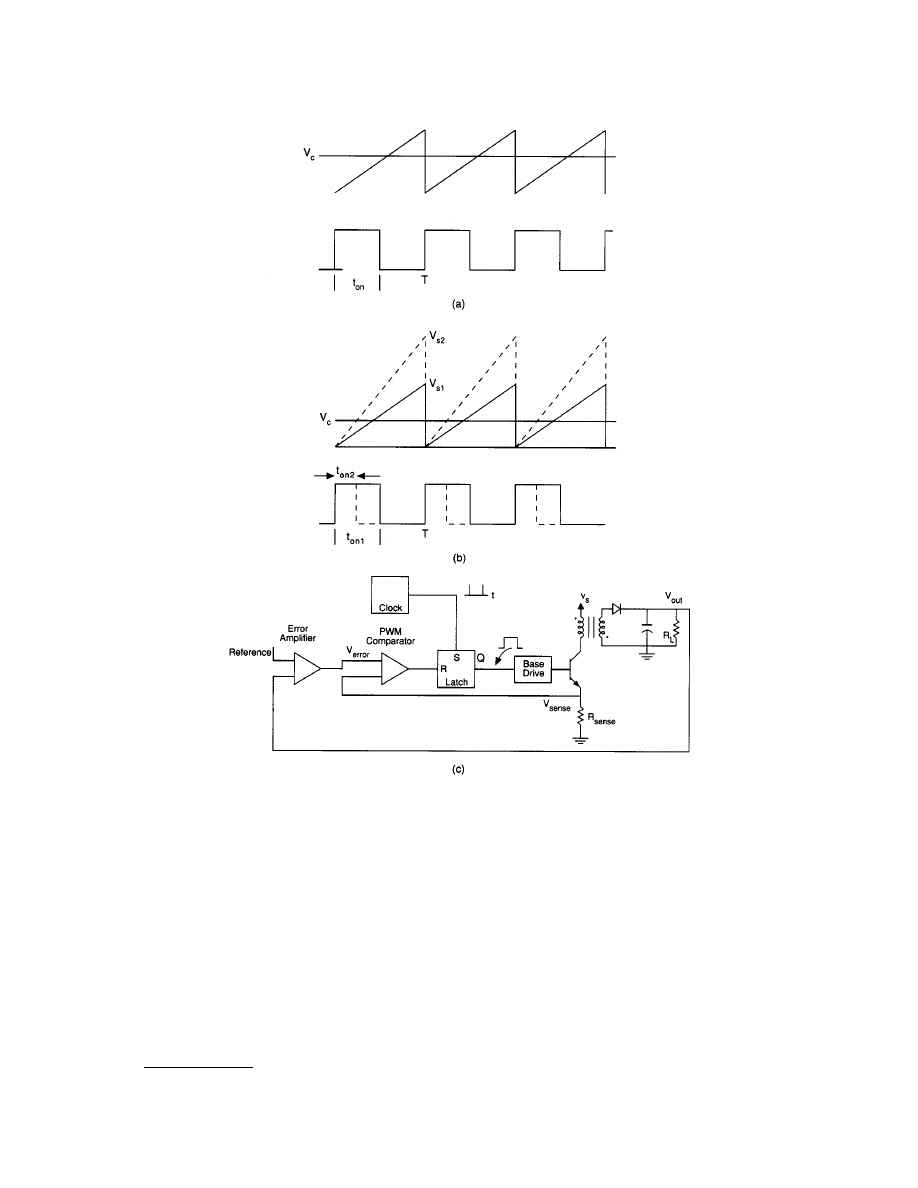
Pulsewidth-Modulated Converters
These converters employ square-wave pulsewidth modulation to achieve voltage regulation. The average output
voltage is varied by varying the duty cycle of the power semiconductor switch. The voltage waveform across
the switch and at the output are square wave in nature [refer to
] and they generally result in
higher switching losses when the switching frequency is increased. Also, the switching stresses are high with
the generation of large electromagnetic interference (EMI), which is difficult to filter. However, these converters
are easy to control, well understood, and have wide load control range.
The methods of control of PWM converters are discussed next.
The Methods of Control. The PWM converters operate with a fixed-frequency, variable duty cycle. Depending
on the duty cycle, they can operate in either continuous current mode (CCM) or discontinuous current mode
(DCM). If the current through the output inductor never reaches zero (refer to Fig. 30.13), then the converter
operates in CCM; otherwise DCM occurs.
The three possible control methods [Severns and Bloom, 1988; Hnatek, 1981; Unitrode Corporation, 1984;
Motorola, 1989; Philips Semiconductors, 1991] are briefly explained below.
1. Direct duty cycle control is the simplest control method. A fixed-frequency ramp is compared with the
control voltage [
] to obtain a variable duty cycle base drive signal for the transistor. This is
the simplest method of control. Disadvantages of this method are (a) provides no voltage feedforward
to anticipate the effects of input voltage changes, slow response to sudden input changes, poor audio
susceptibility, poor open-loop line regulation, requiring higher loop gain to achieve specifications; (b)
poor dynamic response.
2. Voltage feedforward control. In this case the ramp amplitude varies in direct proportion to the input voltage
]. The open-loop regulation is very good, and the problems in 1(a) above are corrected.
3. Current mode control. In this method, a second inner control loop compares the peak inductor current
with the control voltage which provides improved open-loop line regulation [
]. All the
problems of the direct duty cycle control method 1 above are corrected with this method. An additional
advantage of this method is that the two-pole second-order filter is reduced to a single-pole (the filter
capacitor) first-order filter, resulting in simpler compensation networks.
The above control methods can be used in all the PWM converter configurations explained below.
© 2000 by CRC Press LLC
PWM converters can be classified as single-ended and double-ended converters. These converters may or
may not have a high-frequency transformer for isolation.
Nonisolated Single-Ended PWM Converters.
The basic nonisolated single-ended converters are (a) buck
(step-down), (b) boost (step-up), (c) buck-boost (step-up or step-down, also referred to as flyback), and (d)
´Cuk converters (
). The first three of these converters have been discussed in Section 30.2. The ´Cuk
converter provides the advantage of nonpulsating input-output current ripple requiring smaller size external
filters. Output voltage expression is the same as the buck-boost converter (refer to Section 30.2) and can be
less than or greater than the input voltage. There are many variations of the above basic nonisolated converters,
and most of them use a high-frequency transformer for ohmic isolation between the input and the output.
Some of them are discussed below.
FIGURE 30.19
PWM converter control methods: (a) direct duty cycle control; (b) voltage feedforward control; (c) current
mode control (illustrated for flyback converter).
© 2000 by CRC Press LLC
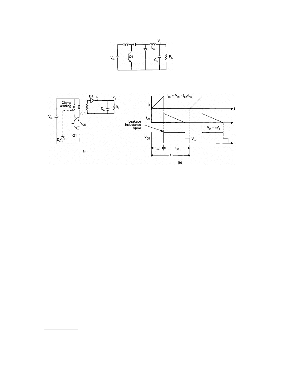
Isolated Single-Ended Topologies
1. The flyback converter (
version of the buck-boost converter. In this converter
(Fig. 30.21), when the transistor is on, energy is stored in the coupled inductor (not a transformer), and
this energy is transferred to the load when the switch is off.
Some of the advantages of this converter are that the leakage inductance is in series with the output
diode when current is delivered to the output, and, therefore, no filter inductor is required; cross
regulation for multiple output converters is good; it is ideally suited for high-voltage output applications;
and it has the lowest cost.
Some of the disadvantages are that large output filter capacitors are required to smooth the pulsating
output current; inductor size is large since air gaps are to be provided; and due to stability reasons,
flyback converters are usually operated in the DCM, which results in increased losses. To avoid the
stability problem, flyback converters are operated with current mode control explained earlier. Flyback
converters are used in the power range of 20 to 200 W.
2. The forward converter (
) is based on the buck converter. It is usually operated in the CCM to
reduce the peak currents and does not have the stability problem of the flyback converter. The HF
transformer transfers energy directly to the output with very small stored energy. The output capacitor
size and peak current rating are smaller than they are for the flyback. Reset winding is required to remove
the stored energy in the transformer. Maximum duty cycle is about 0.45 and limits the control range.
This topology is used for power levels up to about 1 kW.
The flyback and forward converters explained above require the rating of power transistors to be much
higher than the supply voltage. The two-transistor flyback and forward converters shown in
the voltage rating of transistors to the supply voltage.
The Sepic converter shown in
is another isolated single-ended PWM converter.
FIGURE 30.20
Nonisolated ´
Cuk converter.
FIGURE 30.21
(a) Flyback converter. The clamp winding shown is optional and is used to clamp the transistor voltage
stress to V
in
+ nV
o
. (b) Flyback converter waveforms without the clamp winding. The leakage inductance spikes vanish with
the clamp winding.
© 2000 by CRC Press LLC
Double-Ended PWM Converters.
Usually, for power levels above 300 W, double-ended converters are used.
In double-ended converters, full-wave rectifiers are used and the output voltage ripple will have twice the
switching frequency. Three important double-ended PWM converter configurations are push-pull (
half-bridge (
FIGURE 30.22
(a) Forward converter. The clamp winding shown is required for operation. (b) Forward converter waveforms.
FIGURE 30.23
(a) Two-transistor single-ended flyback converter. (b) Two-transistor single-ended forward converter.
FIGURE 30.24
Sepic converter.
© 2000 by CRC Press LLC
1. The push-pull converter. The duty ratio of each transistor in a push-pull converter (Fig. 30.25) is less
than 0.5. Some of the advantages are that the transformer flux swings fully, thereby the size of the
transformer is much smaller (typically half the size) than single-ended converters, and output ripple is
twice the switching frequency of transistors, allowing smaller filters.
Some of the disadvantages of this configuration are that transistors must block twice the supply voltage,
flux symmetry imbalance can cause transformer saturation and special control circuitry is required to
avoid this problem, and use of center-tap transformer requires extra copper resulting in higher volt-
ampere (VA) rating.
FIGURE 30.25
(a) Push-pull converter and (b) its operating waveforms.
FIGURE 30.26
Half-bridge converter. Coupling capacitor C
c
is used to avoid transformer saturation.
© 2000 by CRC Press LLC
Current mode control (for the primary current) can be used to overcome the flux imbalance. This
configuration is used in 100- to 500-W output range.
2. The half-bridge. In the half-bridge configuration (Fig. 30.26) center-tapped dc source is created by two
smoothing capacitors (C
in
), and this configuration utilizes the transformer core efficiently. The voltage
across each transistor is equal to the supply voltage (half of push-pull) and, therefore, is suitable for
high-voltage inputs. One salient feature of this configuration is that the input filter capacitors can be
used to change between 110/220-V mains as selectable inputs to the supply.
The disadvantage of this configuration is the requirement for large-size input filter capacitors. The
half-bridge configuration is used for power levels of the order of 500 to 1000 W.
3. The full-bridge configuration (
) requires only one smoothing capacitor, and for the same
transistor type as that of half-bridge, output power can be doubled. It is usually used for power levels
above 1 kW, and the design is more costly due to increased number of components (uses four transistors
compared to two in push-pull and half-bridge converters).
One of the salient features of a full-bridge converter is that by using proper control technique it can
be operated in zero-voltage switching (ZVS) mode. This type of operation results in negligible switching
losses. However, at reduced load currents, the ZVS property is lost. Recently, there has been a lot of
effort to overcome this problem.
Resonant Power Supplies
Similar to the PWM converters, there are two types of resonant converters: single-ended and double-ended.
Resonant converter configurations are obtained from the PWM converters explained earlier by adding LC
(inductor-capacitor) resonating elements to obtain sinusoidally varying voltage and/or current waveforms. This
approach reduces the switching losses and the switch stresses during switching instants, enabling the converter to
operate at high switching frequencies, resulting in reduced size, weight, and cost. Some other advantages of resonant
converters are that leakage inductances of HF transformers and the junction capacitances of semiconductors can
FIGURE 30.27
Full-bridge converter.
FIGURE 30.28
(a) Zero-current resonant switch: (i) L-type and (ii) M-type. (b) Half-wave configuration using L-type ZC
resonant switch. (c) Full-wave configuration using L-type ZC resonant switch.
© 2000 by CRC Press LLC
be used profitably in the resonant circuit, and reduced EMI. The major disadvantage of resonant converters is
increased peak current (or voltage) stress.
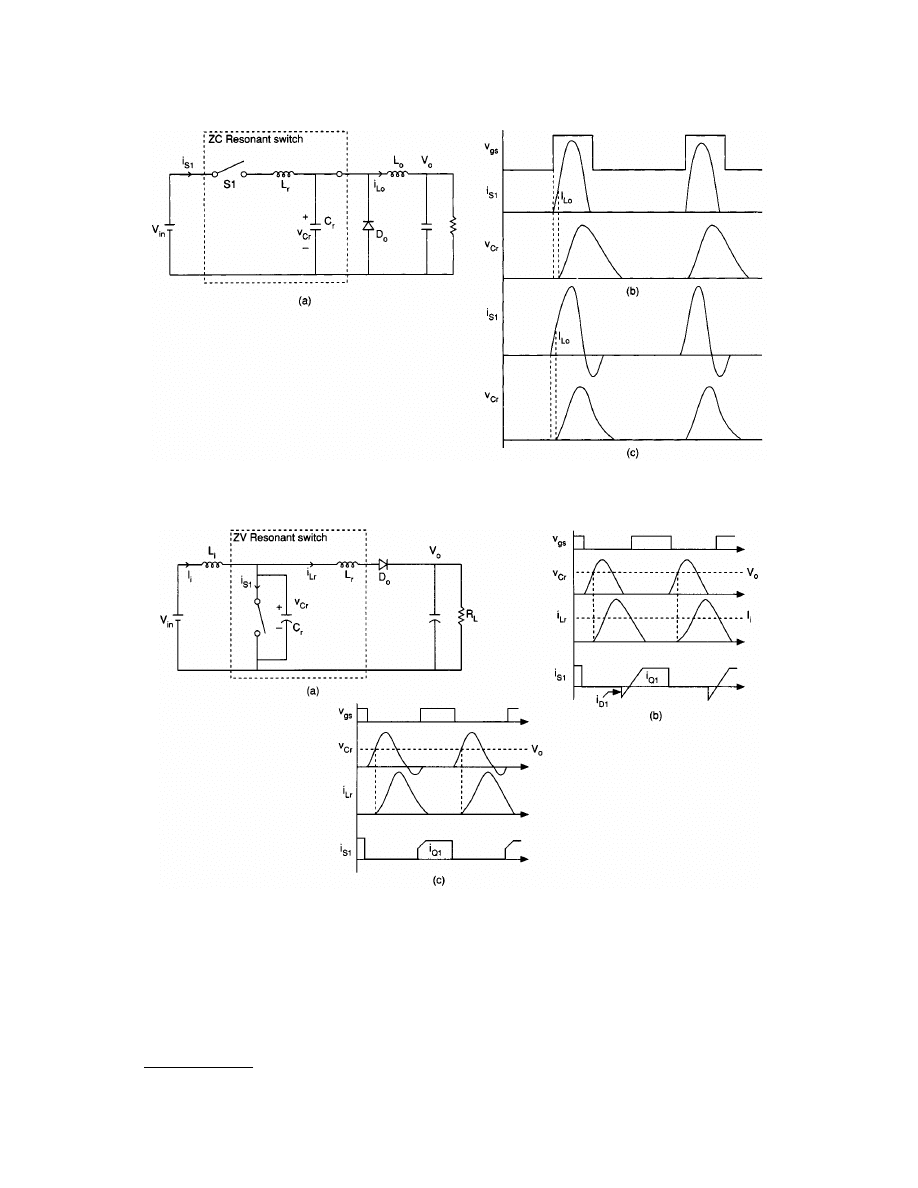
Single-Ended Resonant Converters.
They are referred to as quasi-resonant converters (QRCs) since the voltage
(or current) waveforms are quasi-sinusoidal in nature. The QRCs can operate with zero-current switching
(ZCS) or ZVS or both. All the QRC configurations can be generated by replacing the conventional switches by
the resonant switches shown in
. A number of configurations are realizable. Basic principles
of ZCS and ZVS are explained briefly below.
1. Zero-current switching QRCs [Sum, 1988; Liu et al., 1985]
.
shows an example of a
ZCS QR buck converter implemented using a ZC resonant switch. Depending on whether the resonant
switch is half-wave type or full-wave type, the resonating current will be only half-wave sinusoidal
[
] or a full sine-wave [Fig. 30.30(c)]. The device currents are shaped sinusoidally, and,
therefore, the switching losses are almost negligible with low turn-on and turn-off stresses. ZCS QRCs
can operate at frequencies of the order of 2 MHz. The major problems with this type of converter are
high peak currents through the switch and capacitive turn-on losses.
2. Zero-voltage switching QRCs [Sum, 1988; Liu and Lee, 1986].
ZVS QRCs are duals of ZCS QRCs. The
auxiliary LC elements are used to shape the switching device’s voltage waveform at off time in order to
create a zero-voltage condition for the device to turn on.
shows an example of ZVS QR
boost converter implemented using a ZV resonant switch. The circuit can operate in the half-wave mode
[
] depending on whether a half-wave or full-wave
ZV resonant switch is used, and the name comes from the capacitor voltage waveform. The full-wave
mode ZVS circuit suffers from capacitive turn-on losses. The ZVS QRCs suffer from increased voltage
stress on the switch. However, they can be operated at much higher frequencies compared to ZCS QRCs.
Double-Ended Resonant Converters.
These converters [Sum, 1988; Bhat, 1991; Steigerwald, 1988; Bhat, 1992]
use full-wave rectifiers at the output, and they are generally referred to as resonant converters. A number of
resonant converter configurations are realizable by using different resonant tank circuits, and the three most
popular configurations, namely, the series resonant converter (SRC), the parallel resonant converter (PRC),
and the series-parallel resonant converter (SPRC) (also called LCC-type PRC), are shown in
Series resonant converters [Fig. 30.32(a)] have high efficiency from full load to part load. Transformer
saturation is avoided due to the series blocking resonating capacitor. The major problems with the SRC are
that it requires a very wide change in switching frequency to regulate the load voltage and the output filter
capacitor must carry high ripple current (a major problem especially in low output voltage, high output current
applications).
Parallel resonant converters [Fig. 30.32(b)] are suitable for low output voltage, high output current applica-
tions due to the use of filter inductance at the output with low ripple current requirements for the filter capacitor.
The major disadvantage of the PRC is that the device currents do not decrease with the load current, resulting
in reduced efficiency at reduced load currents.
FIGURE 30.29
(a) Zero-voltage resonant switches. (b) Half-wave configuration using ZV resonant switch shown in Fig.
(a)(i). (c) Full-wave configuration using ZV resonant switch shown in Fig. (a)(i).
© 2000 by CRC Press LLC
The SPRC [Fig. 30.32(c)] takes the desirable features of SRC and PRC.
Load voltage regulation in resonant converters for input supply variations and load changes is achieved by
either varying the switching frequency or using fixed-frequency (variable pulsewidth) control.
1. Variable-frequency operation.
Depending on whether the switching frequency is below or above the natural
resonance frequency (
w
r
), the converter can operate in different operating modes as explained below.
FIGURE 30.30
(a) Implementation of ZCS QR buck converter using L-type resonant switch. (b) Operating waveforms
for half-wave mode. (c) Operating waveforms for full-wave mode.
FIGURE 30.31
(a) Implementation of ZVS QR buck converter using resonant switch shown in Fig. 30.28(a)(i).
(b) Operating waveforms for half-wave mode. (c) Operating waveforms for full-wave mode.
© 2000 by CRC Press LLC
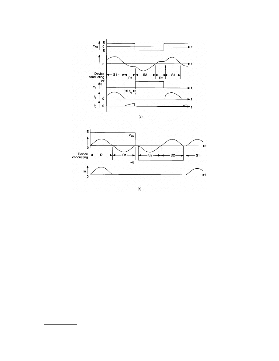
a. Below-resonance (leading PF) mode. When the switching frequency is below the natural resonance
frequency, the converter operates in a below-resonance mode (
). The equivalent impedance
across AB presents a leading PF so that natural turn-off of the switches is assured and any type of fast
turn-off switch (including asymmetric SCRs) can be used. Depending on the instant of turn-on of
switches S
1
and S
2
, the converter can enter into two modes of operation, namely, continuous and
discontinuous current modes. The steady-state operation in continuous current mode (CCM)
[Fig. 30.33(a)] is explained briefly as follows.
Assume that diode D
2
was conducting and switch S
1
is turned on. The current carried by D
2
will be
transferred to S
1
almost instantaneously (except for a small time of recovery of D
2
during which input
supply is shorted through D
2
and S
1
, and the current is limited by the di/dt limiting inductors). The
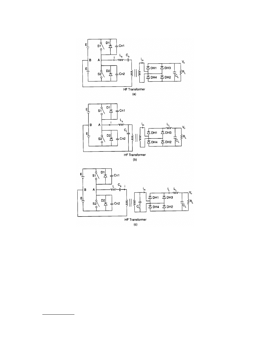
FIGURE 30.32
High-frequency resonant converter (half-bridge version) configurations suitable for operation above res-
onance. Cn1 and Cn2 are the snubber capacitors. (Note: For operation below resonance, di/dt limiting inductors and RC
snubbers are required. For operation above resonance, only capacitive snubbers are required as shown.) (a) Series resonant
converter. Leakage inductances of the HF transformer can be part of resonant inductance. (b) Parallel resonant converter.
(c) Series-parallel (or LCC-type) resonant converter with capacitor C
t
placed on the secondary side of the HF transformer.
© 2000 by CRC Press LLC
current i then oscillates sinusoidally and goes to zero in the natural way. The current tries to reverse,
and the path for this current is provided by the diode D
1
. Conduction of D
1
feeds the reactive energy in
the load and the tank circuit back to the supply. The on-state of D
1
also provides a reverse voltage across
S
1
, allowing it to turn off. After providing a time equal to or greater than the turn-off time of S
1
, switch
S
2
can be turned on to initiate the second half cycle. The process is similar to the first half cycle, with
the voltage across v
AB
being of opposite polarity, and the functions of D
1
, S
1
will be assumed by D
2
, S
2
.
With this type of operation, the converter works in the continuous current mode as the switches are
turned on before the currents in the diodes reach zero. If the switching on of S
1
and S
2
is delayed such
that the currents through the previously conducting diodes reach zero, then there are zero current
intervals and the
operates in the DCM [Fig. 30.33(b)].
Load voltage regulation is achieved by decreasing the switching frequency below the rated value. Since
the inverter output current i leads the inverter output voltage v
AB
, this type of operation is also called a
leading PF mode of operation. If transistors are used as the switching devices, then for operation in
DCM, the pulsewidth can be kept constant while decreasing the switching frequency to avoid CCM
operation. DCM operation has the advantages of negligible switching losses due to ZCS, lower di/dt and
dv/dt stresses, and simple control circuitry. However, DCM operation results in higher switch peak currents.
From the waveforms shown in Fig. 30.33, the following problems can be identified for operation in
the below-resonance mode: requirement of di/dt inductors to limit the large turn-on switch currents
and a need for lossy RC snubbers and fast recovery diodes. Since the switching frequency is decreased
to control the load power, the HF transformer and magnetics must be designed for the lowest switching
frequency, resulting in increased size of the converter.
FIGURE 30.33
Typical waveforms at different points of a resonant converter operating below resonance (a) in continuous
current mode and (b) in discontinuous current mode.
© 2000 by CRC Press LLC
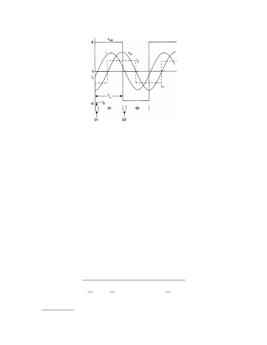
b. Above-resonance (lagging PF) mode.
If switches capable of gate or base turn-off (e.g., MOSFETs,
bipolar transistors) are used, then the converter can operate in the above-resonance mode (lagging PF
mode).
shows some typical operating waveforms for such type of operation, and it can be
noticed that the current i lags the voltage v
AB
. Since the switch takes current from its own diode across
it at zero-current point, there is no need for di/dt limiting inductance, and a simple capacitive snubber
can be used. In addition, the internal diodes of MOSFETs can be used due to the large turn-off time
available for the diodes. Major problems with the lagging PF mode of operation are that there are switch
turn-off losses, and since the voltage regulation is achieved by increasing the switching frequency above
the rated value, the magnetic losses increase and the design of a control circuit is difficult.
Exact analysis of resonant converters is complex due to the nonlinear loading on the resonant tanks.
The rectifier-filter-load resistor block can be replaced by a square-wave voltage source [for SRC,
Fig. 30.32(a)] or a square-wave current source [for PRC and SPRC, Fig. 30.32(b) and (c)]. Using fun-
damental components of the waveforms, an approximate analysis [Bhat, 1991; Steigerwald, 1988] using
a phasor circuit gives a reasonably good design approach. This analysis approach is illustrated next for
the SPRC.
2. Approximate analysis of SPRC.
shows the equivalent circuit at the output of the inverter
and the phasor circuit used for the analysis. All the equations are normalized using the base quantities
Base voltage V
B
= E
min
Base impedance Z
B
= R
¢
L
= n
2
R
L
Base current I
B
= V
B
/I
B
The converter gain [normalized output voltage in per unit (p.u.) referred to the primary-side] can be
derived as [Bhat, 1991; Steigerwald, 1988]
(30.1)
FIGURE 30.34
Typical operating waveforms at different points of an SPRC operating above resonance.
M
C
C
y
Q
y
y
t
s
s
s
s
s
=
æ
è
ç
ö
ø
÷
+
æ
è
ç
ö
ø
÷
-
(
)
é
ë
ê
ê
ù
û
ú
ú
+
-
æ
è
ç
ö
ø
÷
é
ë
ê
ê
ù
û
ú
ú
ì
í
ï
î
ï
ü
ý
ï
þ
ï
1
8
1
1
1
2
2
2
2
2
2
1 2
p
/
p.u.
© 2000 by CRC Press LLC
where
(30.2)
(30.3)
and
(30.4)
The equivalent impedance looking into the terminals AB is given by
(30.5)
where
(30.6)
FIGURE 30.35
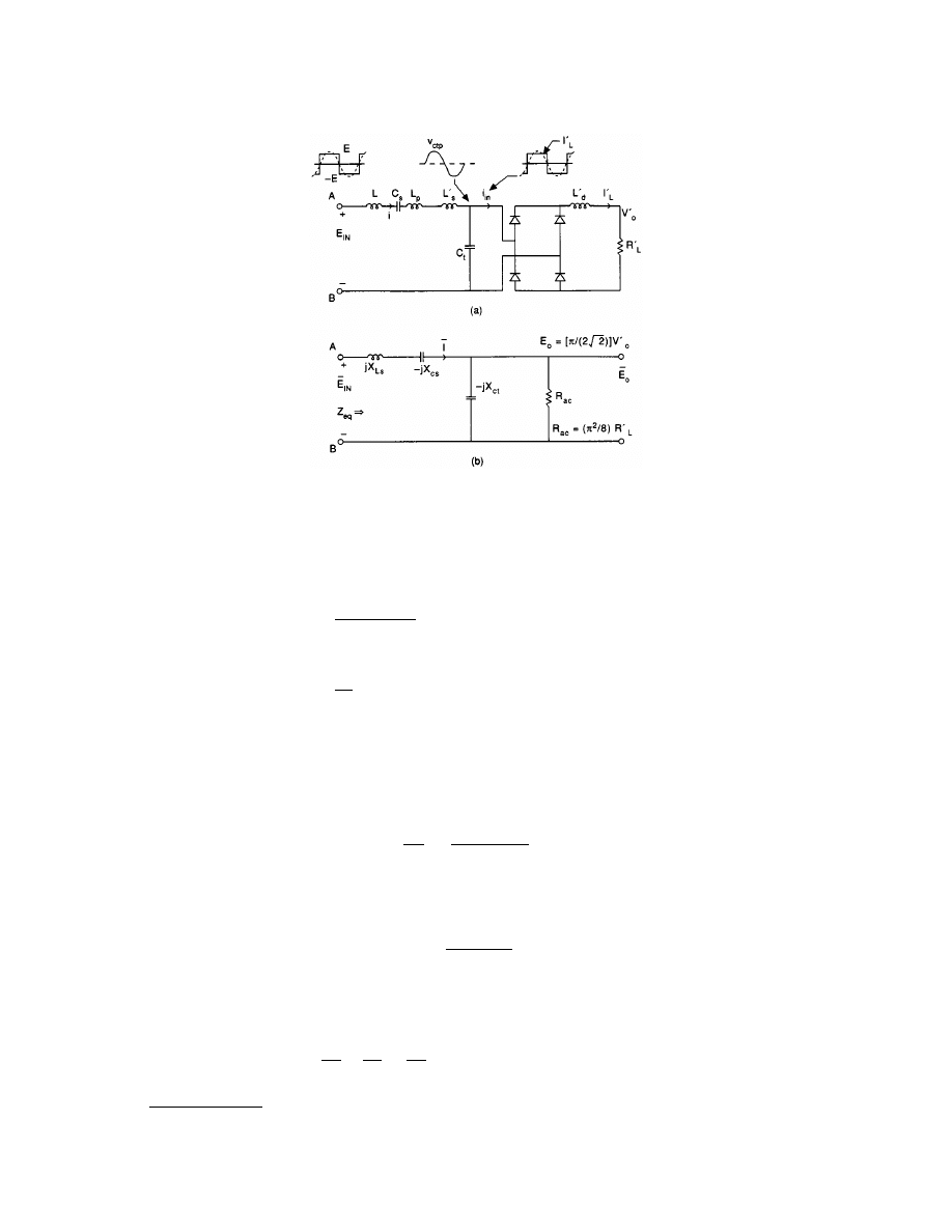
(a) Equivalent circuit for a SPRC at the output of the inverter terminals (across AB) of Fig. 30.31(c), L
p
and L
¢
s
are the leakage inductance of the primary and primary referred leakage inductance of the secondary, respectively.
(b) Phasor circuit model used for the analysis of the SPRC converter.
Q
L
C
R
L
L
L
L
s
s
s
L
s
p
s
=
¢
=
+
+
¢
(
/
)
;
/
1 2
y
f
f
s
s
r
=
f
f
L C
s
r
r
s s
=
=
=
=
switching frequency
series resonance frequency
/
w
p
p
2
1
2
1 2
(
)
Z
B
jB
B
eq
=
+
1
2
3
p.u.
B
C
C
Q
y
s
t
s
s
1
2
2
2
8
=
æ
è
ç
ö
ø
÷
æ
è
ç
ö
ø
÷
æ
è
ç
ö
ø
÷
p

© 2000 by CRC Press LLC
(30.7)
(30.8)
The peak inverter output (resonant inductor) current can be calculated using
(30.9)
The same current flows through the switching devices.
The value of initial current I
0
is given by
I
0
= I
p
sin(–
f ) p.u. (30.10)
where
f = tan
–1
(B
2
/B
1
) rad. B
1
and B
2
are given by Eqs. (30.6) and (30.7), respectively.
If I
0
is negative, then forced commutation is necessary and the converter is operating in the lagging
PF mode. The peak voltage across the capacitor C
¢
t
(on the secondary side) is
(30.11)
The peak voltage across C
s
and the peak current through C
¢
t
are given by
(30.12)
(30.13)
(30.14)
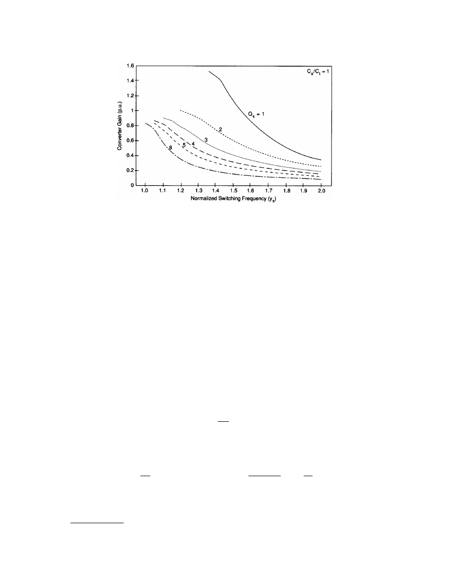
The plot of converter gain versus the switching frequency ratio y
s
, obtained using (30.1), is shown for
C
s
/C
t
= 1 in
, for the lagging PF mode of operation. If the ratio C
s
/C
t
increases, then the
converter takes the characteristics of SRC and the load voltage regulation requires a very wide range in
the frequency change. Lower values of C
s
/C
t
take the characteristics of a PRC. Therefore, a compromised
value of C
s
/C
t
= 1 is chosen.
It is possible to realize higher-order resonant converters with improved characteristics and many of
them are presented in Bhat [1991].
3. Fixed-frequency operation. To overcome some of the problems associated with the variable frequency
control of resonant converters, they are operated with fixed frequency [Sum, 1988; Bhat, 1992]. A number
of configurations and control methods for fixed-frequency operation are available in the literature (Bhat
[1992] gives a list of papers). One of the most popular methods of control is the phase-shift control
B
Q y
y
C
C
Q
y
C
C
Q
y
s
s
s
s
t
s
s
s
t
s
s
2
2
2
2
2
1
1
8
=
-
æ
è
ç
ö
ø
÷
+
æ
è
ç
ö
ø
÷
æ
è
ç
ö
ø
÷
æ
è
ç
ö
ø
÷
é
ë
ê
ê
ù
û
ú
ú
-
æ
è
ç
ö
ø
÷
æ
è
ç
ö
ø
÷
p
B
C
C
Q
y
s
t
s
s
3
2
2 2
2
1
8
=
+
æ
è
ç
ö
ø
÷
æ
è
ç
ö
ø
÷
æ
è
ç
ö
ø
÷
p
I
Z
p
eq
=
4
p
*
*
p.u.
V
V
o
ctp
V
=
p
2
V
Q
y
I
s
s
p
csp
p.u.
=
I
V
X
R
L
ctp
ctp
cptu
A
=
X
C
C
Q
y
s
t
s
s
ctpu
p.u.
=
æ
è
ç
ö
ø
÷
æ
è
ç
ö
ø
÷
© 2000 by CRC Press LLC
(also called clamped-mode or PWM operation) method.
illustrates the clamped-mode
fixed-frequency operation of the SPRC. The load power control is achieved by changing the phase-shift
angle
f between the gating signals to vary the pulsewidth of v
AB
.
4. Design example. Design a 500-W output SPRC (half-bridge version) with secondary-side resonance
(operation in lagging PF mode and variable-frequency control) with the following specifications:
Minimum input supply voltage = 2E
min
= 230 V
Load voltage, V
o
= 48 V
Switching frequency, f
s
= 100 kHz
Maximum load current = 10.42 A
As explained in item 2, C
s
/C
t
= 1 is chosen. Using the constraints (1) minimum kVA rating of tank circuit
per kW output power, (2) minimum inverter output peak current, and (3) enough turn-off time for the
switches, it can be shown that [Bhat, 1991] Q
s
= 4 and y
s
= 1.1 satisfy the design constraints. From
Fig. 30.36, M = 0.8 p.u.
Average load voltage referred to the primary side of the HF transformer = 0.8
2 115 V = 92 V.
Therefore, the transformer turns ratio required
.1.84.
The values of L
s
and C
s
can be obtained by solving
Solving the above equations gives L
s
= 109
mH and C
s
= 0.0281
mF. Leakage inductance (L
p
+ L
¢
s
) of the
HF transformer can be used as part of L
s
. Typical value for a 100-kHz practical transformer (using Tokin
FIGURE 30.36
The converter gain M (p.u.) (normalized output voltage) versus normalized switching frequency y
s
of SPRC
operating above resonance for C
s
/C
t
= 1.
¢ =
æ
è
ç
ö
ø
÷ =
W
R
n
V
P
L
o
o
2
2
15 6
.
L
C L C
f
y
s
s
r
s
s
s
s
æ
è
ç
ö
ø
÷
=
´
=
=
1 2
1 2
4
15 6
1
2
/
/
.
(
)
W and w
p
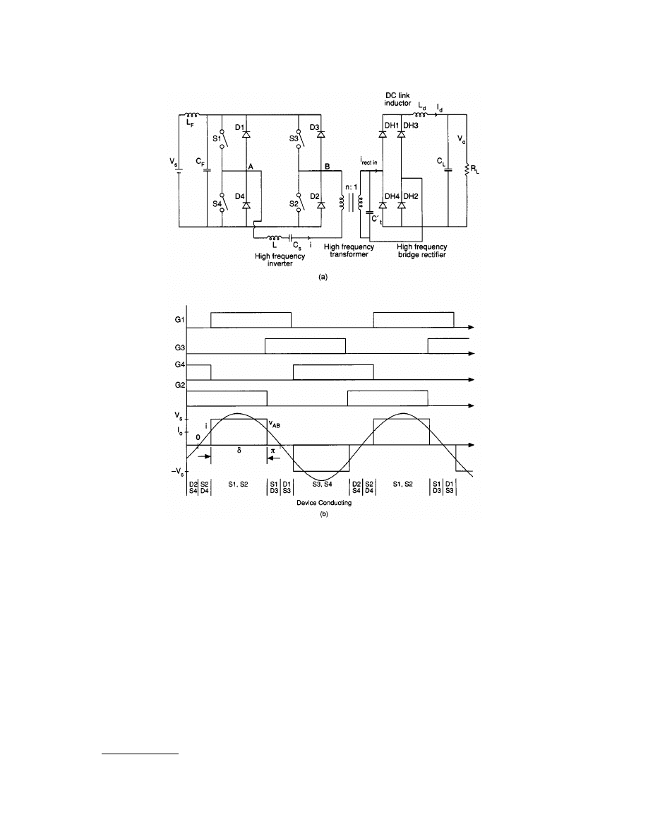
© 2000 by CRC Press LLC
Mn-Zn 2500B2 Ferrite, E-I type core) for this application is about 5
mH. Therefore, the external resonant
inductance required is L = 104
mH.
Since C
s
/C
t
= 1 is chosen, C
t
= 0.0281
mF. The actual value of C
t
used on the secondary side of the
HF transformer = (1.84)
2
2 0.0281 = 0.09514 mF. The resonating capacitors must be HF type (e.g.,
polypropylene) and must be capable of withstanding the voltage and current ratings obtained above
(enough safety margin must be provided).
Using Eqs. (30.9) and (30.11) to (30.13):
Peak current through switches = 7.6 A
Peak voltage across C
s
, V
csp
= 430 V
Peak voltage (on secondary side) across C
¢
t
, V
ctp
= 76 V
Peak current through capacitor C
¢
t
(on secondary side), I
ctp
= 4.54 A
FIGURE 30.37
(a) Basic circuit diagram of series-parallel resonant converter suitable for fixed-frequency operation with
PWM (clamped-mode) control. (b) Waveforms to illustrate the operation of fixed-frequency PWM series-parallel resonant
converter working with a pulsewidth
d.
© 2000 by CRC Press LLC
A simple control circuit can be built using PWM IC SG3525 and TSC429 MOSFET driver ICs.
With the development of digital ICs operating on low-voltage (of the order of 3 V) supplies, use of
MOSFETs as synchronous rectifiers with very low voltage drop (~0.2 V) has become essential [Motorola,
1989] to increase the efficiency of the power supply.
AC Power Supplies
Some applications of ac power supplies are ac motor drives,
uninterruptible power supply (UPS)
used as a standby ac source
for critical loads (e.g., in hospitals, computers), and dc source-
to-utility interface (either to meet peak power demands or to
augment energy by connecting unconventional energy sources
like photovoltaic arrays to the utility line). In ac induction motor
drives, the ac power main is rectified and filtered to obtain a
smooth dc source, and then an inverter (single-phase version is
shown in
) is used to obtain a variable-frequency, vari-
able-voltage ac source. The sinusoidal pulsewidth modulation
technique described in Section 30.2 can be used to obtain a sinu-
soidal output voltage. Some other methods used to get sinusoidal
voltage output are [Rashid, 1988] a number of phase-shifted
inverter outputs summed in an output transformer to get a
stepped waveform that approximates a sine wave and the use of
a bang-bang controller in Fig. 30.38. All these methods use line-
frequency (60 Hz) transformers for voltage translation and iso-
lation purposes. To reduce the size, weight, and cost of such
systems, one can use dc-to-dc converters (discussed earlier) as an intermediate stage.
shows such
a system in block schematic form. One can use an HF inverter circuit (discussed earlier) followed by a
stage. The major problem with these schemes is the reduction in efficiency due to the extra power stage.
shows a typical UPS scheme. The battery shown has to be charged by a separate rectifier circuit.
AC-to-ac conversion can also be achieved using cycloconverters [e.g., Rashid, 1988].
Special Power Supplies
Using the inverters and cycloconverters, it is possible to realize bidirectional ac and dc power supplies. In these
power supplies [Rashid, 1988], power can flow in both directions, i.e., from input to output or from output
to input. It is also possible to control the ac-to-dc converters to obtain sinusoidal line current with unity PF
and low harmonic distortion at the ac source.
FIGURE 30.38
An inverter circuit to obtain variable-voltage, variable-frequency ac source. Using sinusoidal pulsewidth
modulation control scheme, sine-wave ac output voltage can be obtained.
FIGURE 30.39
AC power supplies using HF
switching (PWM or resonant) dc-to-dc converter
as an input stage. HF transformer isolated dc-to-
dc converters can be used to reduce the size and
weight of the power supply. Sinusoidal voltage
output can be obtained using the modulation in
the output inverter stage or in the dc-to-dc con-
verter.
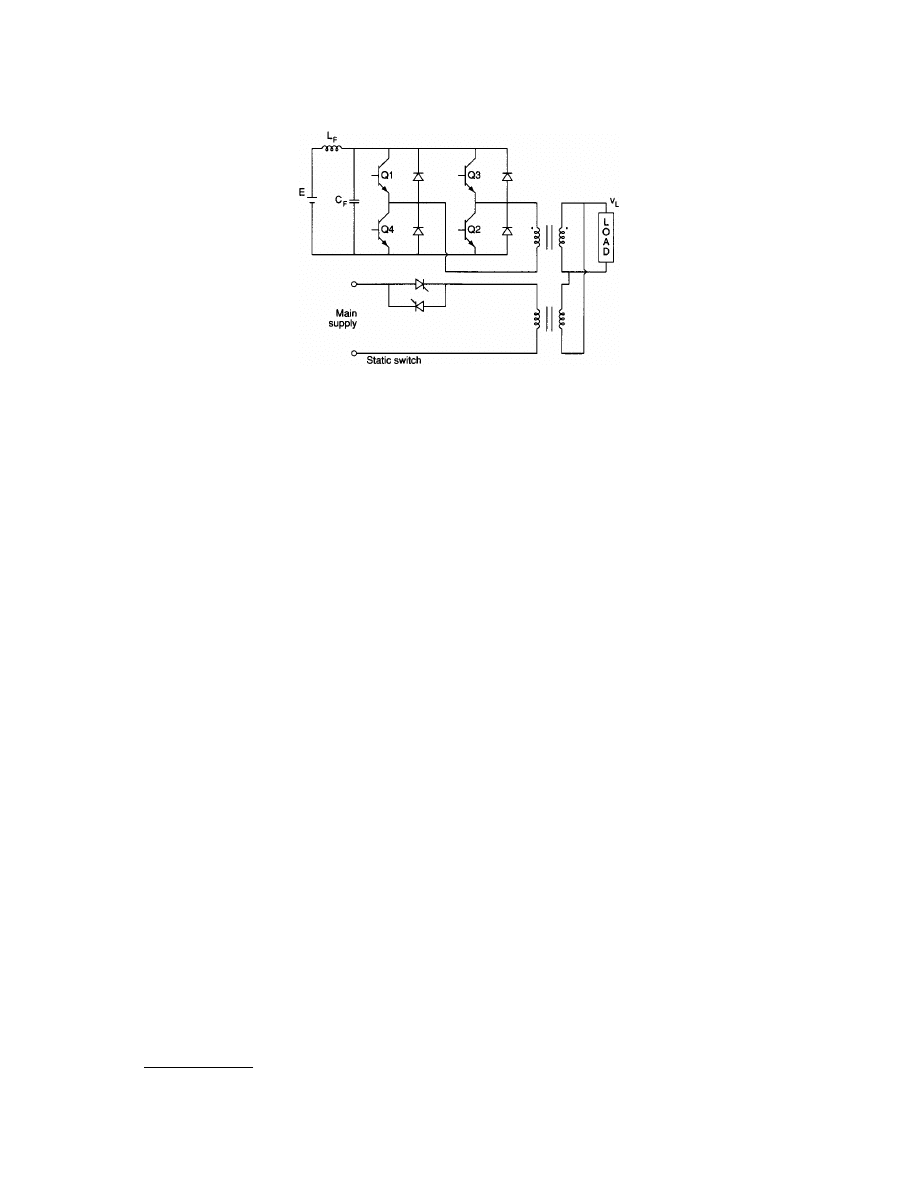
© 2000 by CRC Press LLC
Defining Terms
Converter:
A circuit that performs one of the following power conversions — ac to dc, dc to dc, dc to ac, or
ac to ac.
Cycloconverter:
A power electronic circuit that converts ac input to ac output (generally) of lower frequency
than the input source without using any intermediate dc state.
Inverter:
A power electronic circuit that converts dc input to ac output.
Isolated:
A power electronic circuit that has ohmic isolation between the input source and the load circuit.
Pulsewidth-modulated (PWM) converters:
A power electronic converter that employs square-wave switching
waveforms with variation of pulsewidth for controlling the load voltage.
Regulated output:
Output load voltage is kept at the required value for changes in either the load or the
input supply voltage.
Resonant converters:
A power electronic converter that employs “LC resonant circuits” to obtain sinusoidal
switching waveforms.
Uninterruptible power supply (UPS):
A stand-by dc-to-ac inverter used mostly to provide an emergency
power to loads at mains frequency (50/60 Hz) in the event of a mains failure.
References
A.K.S. Bhat, “A unified approach for the steady-state analysis of resonant converters,” IEEE Trans. Industrial
Electronics, vol. 38, no. 4, pp. 251–259, Aug. 1991.
A.K.S. Bhat, “Fixed frequency PWM series-parallel resonant converter,” IEEE Trans. Industry Applications, vol.
28, no. 5, pp. 1002–1009, 1992.
E.R. Hnatek, Design of Solid-State Power Supplies, 2nd ed., New York: Van Nostrand Reinhold, 1981.
K.H. Liu and F.C. Lee, “Zero-Voltage Switching Technique In DC/DC Converters,” IEEE Power Electronics
Specialists Conference Record, 1986, pp. 58–70.
K.H. Liu, R. Oruganti, and F.C. Lee, “Resonant Switches—Topologies and Characteristics,” IEEE Power Elec-
tronics Specialists Conference Record, 1985, pp. 106–116.
Motorola, Linear/Switchmode Voltage Regulator Handbook, 1989.
Philips Semiconductors, Power Semiconductor Applications, 1991.
M.H. Rashid, Power Electronics: Circuits, Devices, and Applications, Englewood Cliffs, N.J.: Prentice-Hall, 1988.
R. Severns and G. Bloom, Modern Switching DC-to-DC Converters, New York: Van Nostrand Reinhold, 1988.
R.L. Steigerwald, “A comparison of half-bridge resonant converter topologies,” IEEE Trans. Power Electron., vol.
PE-3, no. 2, pp. 174–182, April 1988.
K.K. Sum, Recent Developments in Resonant Power Conversion, Calif.: Intertech Communications, 1988.
Unitrode Switching Regulated Power Supply Design Seminar Manual, Lexington, Mass.: Unitrode Corporation, 1984.
FIGURE 30.40
A typical arrangement of UPS system. The load gets power through the static switch when the ac main
supply is present. The inverter supplies power when the main supply fails.
© 2000 by CRC Press LLC
Further Information
The following monthly magazines and conference records publish papers on the analysis, design, and experi-
mental aspects of power supply configurations and their applications:
IEEE Transactions on Power Electronics, IEEE Transactions on Industrial Electronics, IEEE Transactions on Industry
Applications, and IEEE Transactions on Aerospace and Electronic Systems.
IEEE Power Electronics Specialists Conference Records, IEEE Applied Power Electronics Conference Records, IEEE
Industry Applications Conference Records, and IEEE International Telecommunications Energy Conference
Records.
30.4 Converter Control of Machines
Bimal K. Bose
Converter-controlled electrical machine drives are very important in modern industrial applications. Some
examples in the high-power range are metal rolling mills, cement mills, and gas line compressors. In the
medium-power range are textile mills, paper mills, and subway car propulsion. Machine tools and computer
peripherals are examples of converter-controlled electrical machine drive applications in the low-power range.
The converter normally provides a variable-voltage dc power source for a dc motor drive and a variable-
frequency, variable-voltage ac power source for an ac motor drive. The drive system efficiency is high because
the converter operates in switching mode using power semiconductor devices. The primary control variable of
the machine may be torque, speed, or position, or the converter can operate as a solid-state starter of the
machine. The recent evolution of high-frequency power semiconductor devices and high-density and econom-
ical microelectronic chips, coupled with converter and control technology developments, is providing a tre-
mendous boost in the applications of drives.
Converter Control of DC Machines
The speed of a dc motor can be controlled by controlling the dc voltage across its armature terminals. A phase-
controlled thyristor converter can provide this dc voltage source. For a low-power drive, a single-phase bridge
converter can be used, whereas for a high-power drive, a three-phase bridge circuit is preferred. The machine
can be a permanent magnet or wound field type. The wound field type permits variation and reversal of field
and is normally preferred in large power machines.
Phase-Controlled Converter DC Drive
shows a dc drive using a three-phase thyristor bridge converter. The converter rectifies line ac
voltage to variable dc output voltage by controlling the firing angle of the thyristors. With rated field excitation,
as the armature voltage is increased, the machine will develop speed in the forward direction until the rated,
or base, speed is developed at full voltage when the firing angle is zero. The motor speed can be increased
further by weakening the field excitation. Below the base speed, the machine is said to operate in constant
FIGURE 30.41
Three-phase thyristor bridge converter control of a dc machine.
© 2000 by CRC Press LLC
torque region, whereas the field weakening mode is defined as the constant power region. At any operating
speed, the field can be reversed and the converter firing angle can be controlled beyond 90 degrees for
mode operation of the drive. In this mode, the motor acts as a generator (with negative
induced voltage) and the converter acts as an inverter so that the mechanical energy stored in the inertia is
converted to electrical energy and pumped back to the source. Such
operation gives improved
efficiency if the drive accelerates and decelerates frequently. The speed of the machine can be controlled with
precision by a feedback loop where the command speed is compared with the machine speed measured by a
tachometer. The speed loop error generally generates the armature current command through a compensator.
The current is then feedback controlled with the firing angle control in the inner loop. Since torque is
proportional to armature current (with fixed field), a current loop provides direct torque control, and the drive
can accelerate or decelerate with the rated torque. A second bridge converter can be connected in antiparallel
so that the dual converter can control the machine speed in all the four quadrants (motoring and regeneration
in forward and reverse speeds).
Pulsewidth Modulation Converter DC Machine Drive
speed control of a dc drive is also possible using an H-bridge pulsewidth modulation (PWM)
converter as shown in
. Such drives (using a permanent magnet dc motor) are popular in low-power
applications, such as robotic and instrumentation drives. The dc source can be a battery or may be obtained
from ac supply through a diode rectifier and filter. With PWM operation, the drive response is very fast and
the armature current ripple is small, giving less harmonic heating and torque pulsation. Four-quadrant oper-
ation can be summarized as follows:
Quadrant 1: Forward motoring (buck or step-down converter mode)
Q
1
—on
Q
3
, Q
4
—off
Q
2
—chopping
Current freewheeling through D
3
and Q
1
Quadrant 2: Forward regeneration (boost or step-up converter mode)
Q
1
, Q
2
, Q
3
—off
Q
4
—chopping
Current freewheeling through D
1
and D
2
Quadrant 3: Reverse motoring (buck converter mode)
Q
3
—on
Q
1
, Q
2
—off
Q
4
—chopping
Current freewheeling through D
1
and Q
3
Quadrant 4: Reverse regeneration (boost converter mode)
Q
1
, Q
3
, Q
4
—off
Q
2
—chopping
Current freewheeling through D
3
and D
4
FIGURE 30.42
Four-quadrant dc motor drive using an H-bridge converter.
© 2000 by CRC Press LLC
Often a drive may need only a one- or two-quadrant mode of operation. In such a case, the converter topology
can be simple. For example, in one-quadrant drive, only Q
2
chopping and D
3
freewheeling devices are required,
and the terminal A is connected to the supply positive. Similarly, a two-quadrant drive will need only one leg
of the bridge, where the upper device can be controlled for motoring mode and the lower device can be
controlled for regeneration mode.
Converter Control of AC Machines
Although application of dc drives is quite common, disadvantages are that the machines are bulky and expensive,
and the commutators and brushes require frequent maintenance. In fact, commutator sparking prevents
machine application in an unclean environment, at high speed, and at high elevation. AC machines, particularly
the cage-type induction motor, are favorable when compared with all the features of dc machines. Although
converter system, control, and signal processing of ac drives is definitely complex, the evolution of ac drive
technology in the past two decades has permitted more economical and higher performance ac drives. Conse-
quently, ac drives are finding expanding applications, pushing dc drives towards obsolescence.
Voltage-Fed Inverter Induction Motor Drive
A simple and popular converter system for speed control of an induction motor is shown in
front-end diode rectifier converts 60 Hz ac to dc, which is then filtered to remove the ripple. The dc voltage is
then converted to variable-frequency, variable-voltage output for the machine through a PWM bridge inverter.
Among a number of PWM techniques, the sinusoidal PWM is common, and it is illustrated in
one phase only. The stator sinusoidal reference phase voltage signal is compared with a high-frequency carrier
wave, and the comparator logic output controls switching of the upper and lower transistors in a phase leg.
The phase voltage wave shown refers to the fictitious center tap of the filter capacitor. With the PWM technique,
the fundamental voltage and frequency can be easily varied. The stator voltage wave contains high-frequency
ripple, which is easily filtered by the machine leakage inductance. The voltage-to-frequency ratio is kept constant
to provide constant airgap flux in the machine. The machine voltage-frequency relation, and the corresponding
torque, stator current, and slip, are shown in
. Up to the base or rated frequency
w
b
, the machine can
develop constant torque. Then, the field flux weakens as the frequency is increased at constant voltage. The
speed of the machine can be controlled in a simple open-loop manner by controlling the frequency and
maintaining the proportionality between the voltage and frequency. During acceleration, machine-developed
torque should be limited so that the inverter current rating is not exceeded. By controlling the frequency, the
operation can be extended in the field weakening region. If the supply frequency is controlled to be lower than
the machine speed (equivalent frequency), the motor will act as a generator and the inverter will act as a rectifier,
and energy from the motor will be pumped back to the dc link. The
buck converter with resistive load that dissipates excess power to maintain the dc bus voltage constant. When
FIGURE 30.43
Diode rectifier PWM inverter control of an induction motor.
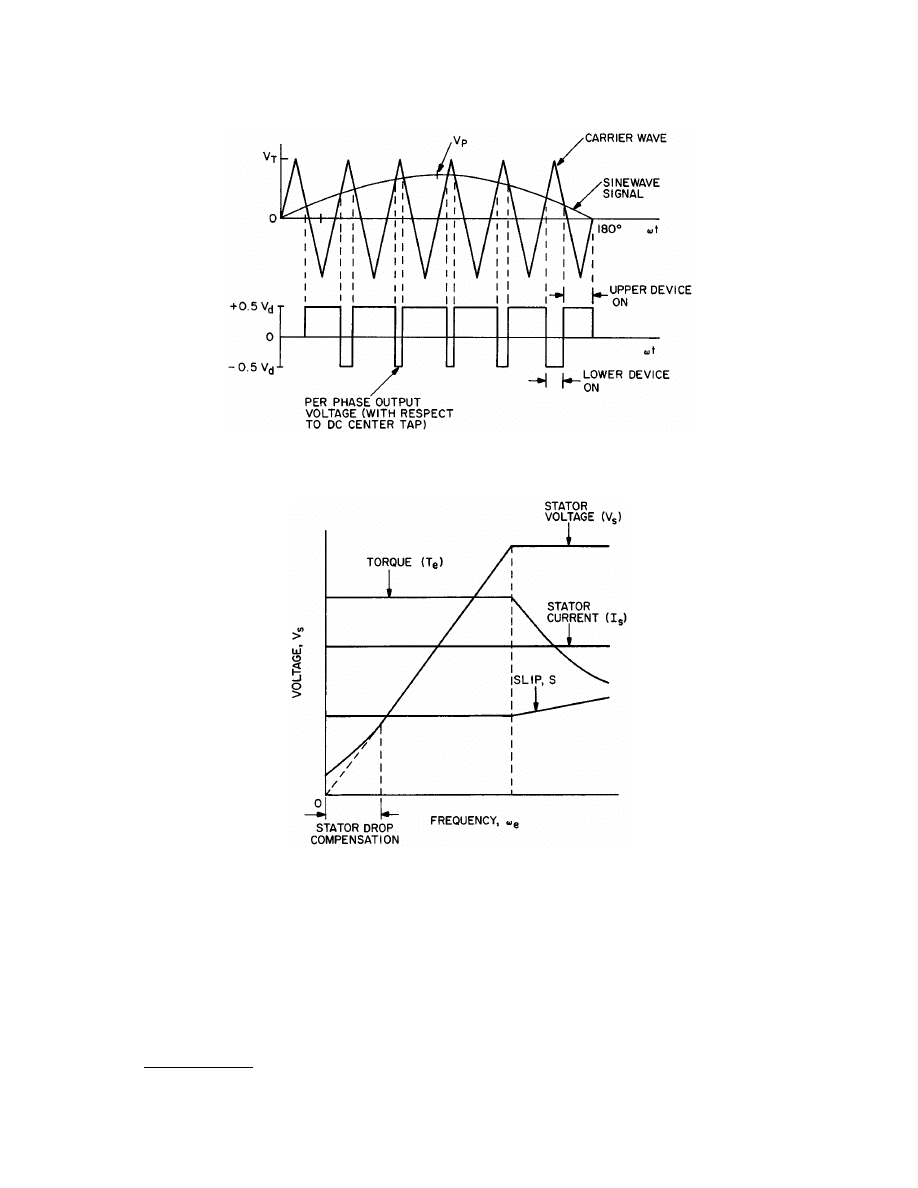
© 2000 by CRC Press LLC
the motor speed is reduced to zero, the phase sequence of the inverter can be reversed for speed reversal.
Therefore, the machine speed can be easily controlled in all four quadrants.
Current-Fed Inverter Induction Motor Drive
The speed of a machine can be controlled by a current-fed inverter as shown in
. The front-end
thyristor rectifier generates a variable dc current source in the dc link inductor. The dc current is then converted
to six-step machine current wave through the inverter. The basic mode of operation of the inverter is the same
as that of the rectifier, except that it is
, that is, the capacitors and series diodes help
commutation of the thyristors. One advantage of the drive is that regenerative braking is easy because the
FIGURE 30.44
Sinusoidal pulse width modulation principle.
FIGURE 30.45
Voltage-frequency relation of an induction motor.
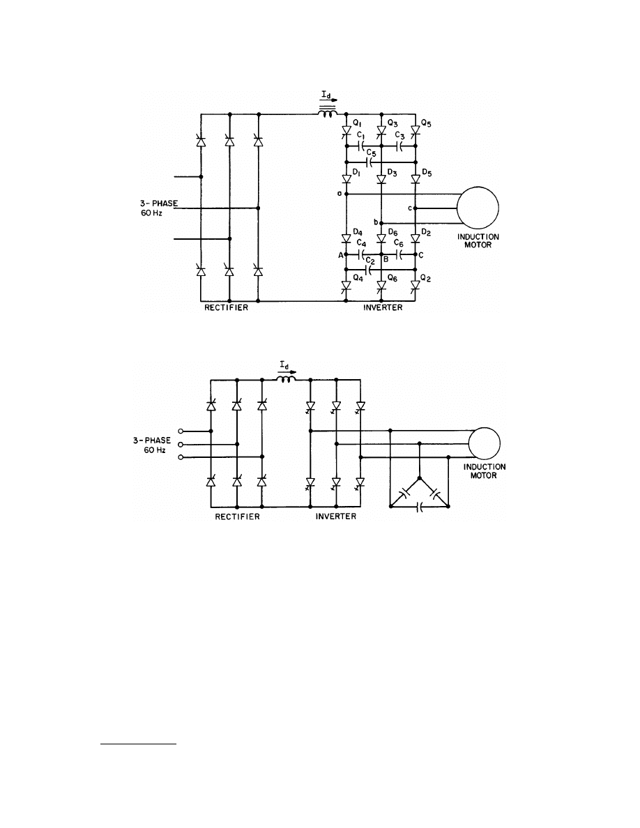
© 2000 by CRC Press LLC
rectifier and inverter can reverse their operation modes. Six-step machine current, however, causes large
harmonic heating and torque pulsation, which may be quite harmful at low-speed operation. Another disad-
vantage is that the converter system cannot be controlled in open loop like a voltage-fed inverter.
Current-Fed PWM Inverter Induction Motor Drive
The force-commutated thyristor inverter in Fig. 30.46 can be replaced by a
(GTO) thyristor PWM inverter as shown in
. The output capacitor bank shown has two functions:
(1) it permits PWM switching of the GTO by diverting the load inductive current, and (2) it acts as a low-pass
filter causing sinusoidal machine current. The second function improves machine efficiency and attenuates the
irritating magnetic noise. Note that the fundamental machine current is controlled by the front-end rectifier,
and the fixed PWM pattern is for controlling the harmonics only. The GTO is to be the reverse-blocking type.
Such drives are popular in the multimegawatt power range. For lower power, an
or transistor can be used with a series diode.
FIGURE 30.46
Force-commutated current-fed inverter control of an induction motor.
FIGURE 30.47
PWM current-fed inverter control of an induction motor.
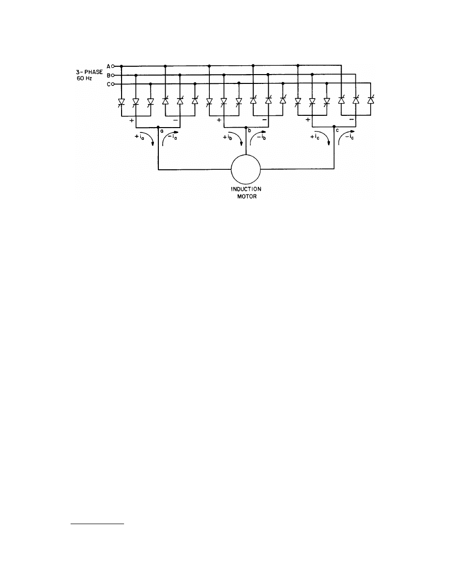
© 2000 by CRC Press LLC
Cycloconverter Induction Motor Drive
A phase-controlled cycloconverter can be used for speed control of an ac machine (induction or synchronous
type).
shows a drive using a three-pulse half-wave or 18-thyristor cycloconverter. Each output
phase group consists of positive and negative converter components which permit bidirectional current flow.
The firing angle of each converter is sinusoidally modulated to generate the variable-frequency, variable-voltage
output required for ac machine drive. Speed reversal and regenerative mode operation are easy. The cyclocon-
verter can be operated in blocking or circulating current mode. In blocking mode, the positive or negative
converter is enabled, depending on the polarity of the load current. In circulating current mode, the converter
components are always enabled to permit circulating current through them. The circulating current reactor
between the positive and negative converter prevents short circuits due to ripple voltage. The circulating current
mode gives simple control and a higher range of output frequency with lower harmonic distortion.
Slip Power Recovery Drive of Induction Motor
In a cage-type induction motor, the rotor current at slip frequency reacting with the airgap flux develops the
torque. The corresponding slip power is dissipated in the rotor resistance. In a wound rotor induction motor,
the slip power can be controlled to control the torque and speed of a machine.
shows a popular
slip power-controlled drive, known as a static Kramer drive. The slip power is rectified to dc with a diode
rectifier and is then pumped back to an ac line through a thyristor phase-controlled inverter. The method
permits speed control in the subsynchronous speed range. It can be shown that the developed machine torque
is proportional to the dc link current I
d
and the voltage V
d
varies directly with speed deviation from the
synchronous speed. The current I
d
is controlled by the firing angle of the inverter. Since V
d
and V
I
voltages
balance at steady state, at synchronous speed the voltage V
d
is zero and the firing angle is 90 degrees. The firing
angle increases as the speed falls, and at 50% synchronous speed the firing angle is near 180 degrees. This is
practically the lowest speed in static Kramer drive. The transformer steps down the inverter input voltage to
get a 180-degree firing angle at lowest speed. The advantage of this drive is that the converter rating is low
compared with the machine rating. Disadvantages are that the line power factor is low and the machine is
expensive. For limited speed range applications, this drive has been popular.
Wound Field Synchronous Motor Drive
The speed of a wound field synchronous machine can be controlled by a current-fed converter scheme as shown
in Fig. 30.46, except that the forced-commutation elements can be removed. The machine is operated at leading
power factor by overexcitation so that the inverter can be load commutated. Because of the simplicity of
converter topology and control, such a drive is popular in the multimegawatt range.
FIGURE 30.48
Cycloconverter control of an induction motor.
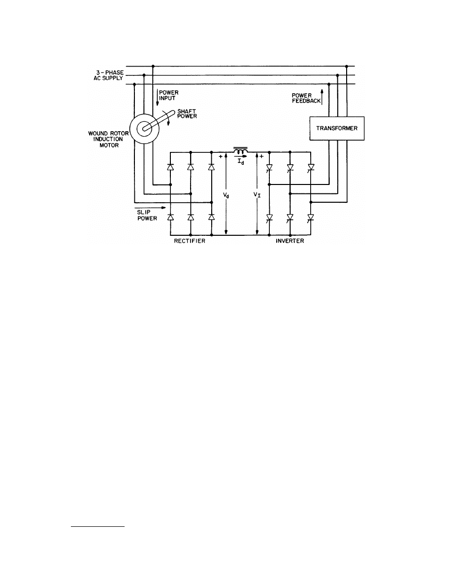
© 2000 by CRC Press LLC
Permanent Magnet Synchronous Motor Drive
Permanent magnet (PM) machine drives are quite popular in the low-power range. A PM machine can have
sinusoidal or concentrated winding, giving the corresponding sinusoidal or trapezoidal induced stator voltage
wave.
shows the speed control system using a trapezoidal machine, and
explains the
wave forms. The power MOSFET inverter supplies variable-frequency, variable-magnitude six-step current
wave to the stator. The inverter is self-controlled, that is, the firing pulses are generated by the machine position
sensor through a decoder. It can be shown that such a drive has the features of dc drive and is normally defined
as brushless dc drive. The speed control loop generates the dc current command, which is then controlled by
the
method to construct the six-step phase current waves in correct phase relation with the
induced voltage waves as shown in Fig. 30.51. The drive can easily operate in four-quadrant mode.
Defining Terms
Dynamic brake: The braking operation of a machine by extracting electrical energy and then dissipating it
in a resistor.
Forced-commutation: Switching off a power semiconductor device by external circuit transient.
Four-quadrant:
A drive that can operate as a motor as well as a generator in both directions.
Hysteresis-band:
A method of controlling current where the instantaneous current can vary within a band.
Insulated gate bipolar transistor (IGBT): A device that combines the features of a power transistor and
MOSFET.
Regenerative braking:
The braking operation of a machine by converting its mechanical energy into electrical
form and then pumping it back to the source.
Self-commutation:
Switching off a power semiconductor device by its gate or base drive.
Two-quadrant:
A drive that can operate as a motor as well as a generator in one direction.
Related Topics
66.1 Generators • 66.2 Motors
FIGURE 30.49
Slip power recovery control of a wound rotor induction motor.
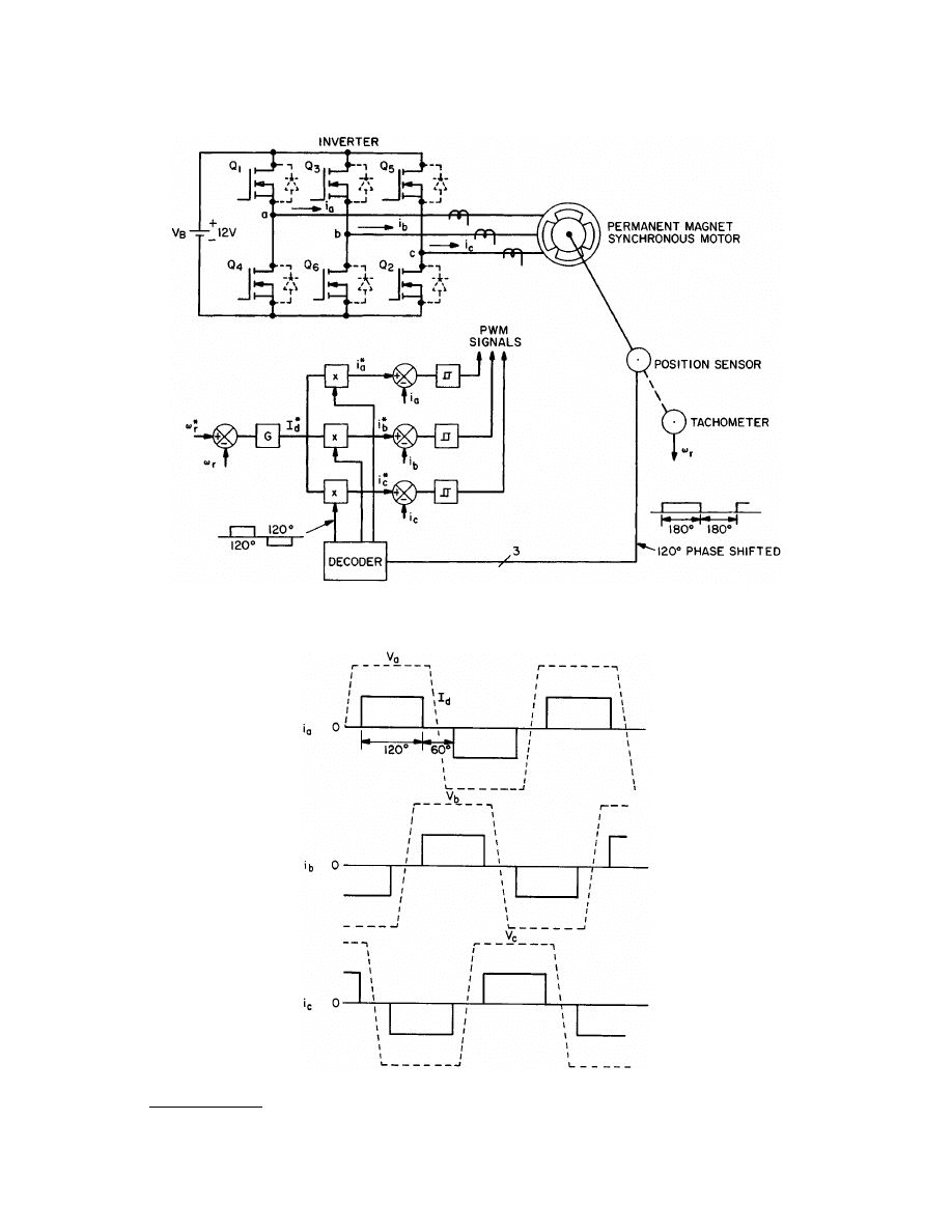
© 2000 by CRC Press LLC
FIGURE 30.50
Permanent magnet synchronous motor control with PWM inverter.
FIGURE 30.51
Phase voltage and current waves in brushless dc drive.

© 2000 by CRC Press LLC
References
B.K. Bose, Power Electronics and AC Drives, Englewood Cliffs, N.J.: Prentice-Hall, 1986.
B.K. Bose, “Adjustable speed AC drives—A technology status review,” Proc. IEEE, vol. 70, pp. 116–135, Feb. 1982.
B.K. Bose, Modern Power Electronics, New York: IEEE Press, 1992.
J.M.D. Murphy and F.G. Turnbull, Power Electronic Control of AC Motors, New York: Pergamon Press, 1988.
P.C. Sen, Thyristor DC Drives, New York: John Wiley, 1981.
Document Outline
- Contents
- Power Electronics
- 30.1Power Semiconductor Devices
- 30.2Power Conversion
- 30.3Power Supplies
- 30.4Converter Control of Machines
- Converter Control of DC Machines
- Phase-Controlled Converter DC Drive
- Pulsewidth Modulation Converter DC Machine Drive
- Converter Control of AC Machines
- Voltage-Fed Inverter Induction Motor Drive
- Current-Fed Inverter Induction Motor Drive
- Current-Fed PWM Inverter Induction Motor Drive
- Cycloconverter Induction Motor Drive
- Slip Power Recovery Drive of Induction Motor
- Wound Field Synchronous Motor Drive
- Permanent Magnet Synchronous Motor Drive
- Converter Control of DC Machines
Wyszukiwarka
Podobne podstrony:
Innovative Solutions In Power Electronics For Variable Speed Wind Turbines
02 E63 64 Body Electrical
AGH Analog electronics Chapter III 5 Power amplifiers
0 50V 2A LM10C, 0 50V 2A Bench power supply circuit diagrams, schematics, electronic projects
Home Power Magazine Betting the Farm Wind Electricity Pays Off
64 SUN ROOF POWER
AGH Analog electronics Chapter IV power supplies
Alternator Secrets Electrical Generator Power
US Patent 382,281 Electrical Transmission Of Power
(ebook electronics) Schematics Power Regulated Power Supply for CB & Ham Radio
SI 8033JD, SI 8050JD, SI 8090JD Surface Mount, Separate Excitation Switching Type Power Supply ICes
Home Power Magazine Before Generating Electricity, Calculate The Load You Will Need (Analysi
US Patent 382,280 Electrical Transmission Of Power
Home Power Magazine Issue 109 Extract pg22 Making Sense of Solar Electricity Costs
US Patent 487,796 System Of Electrical Transmission Of Power
The Market for Microturbine Electrical Power Generation
US Patent 511,559 Electrical Transmission Of Power
więcej podobnych podstron