5-1
FAST AND LS TTL DATA
ONE-OF-TEN DECODER
The LSTTL / MSI SN54 / 74LS42 is a Multipurpose Decoder designed to ac-
cept four BCD inputs and provide ten mutually exclusive outputs. The LS42
is fabricated with the Schottky barrier diode process for high speed and is
completely compatible with all Motorola TTL families.
•
Multifunction Capability
•
Mutually Exclusive Outputs
•
Demultiplexing Capability
•
Input Clamp Diodes Limit High Speed Termination Effects
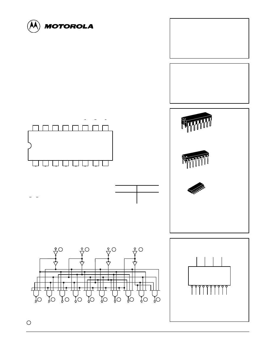
14
13
12
11
10
9
1
2
3
4
5
6
VCC
7
16
15
8
A0
A1
A2
A3
9
8
7
0
1
2
3
4
5
6
GND
NOTE:
The Flatpak version has the
same pinouts (Connection
Diagram) as the Dual In-Line
Package.
CONNECTION DIAGRAM DIP (TOP VIEW)
PIN NAMES
LOADING (Note a)
HIGH
LOW
A0 – A3
0 to 9
Address Inputs
Outputs, Active LOW (Note b)
0.5 U.L.
10 U.L.
0.25 U.L.
5(2.5) U.L.
NOTES:
a) 1 TTL Unit Load (U.L.) = 40
µ
A HIGH/1.6 mA LOW.
b) The Output LOW drive factor is 2.5 U.L. for Military (54) and 5 U.L. for Commercial (74)
Temperature Ranges.
3
LOGIC DIAGRAM
14
4
5
10
11
12
13
15
1
2
6
7
9
1
2
3
4
5
6
0
A0
A1
A2
A3
9
8
7
VCC = PIN 16
GND = PIN 8
= PIN NUMBERS
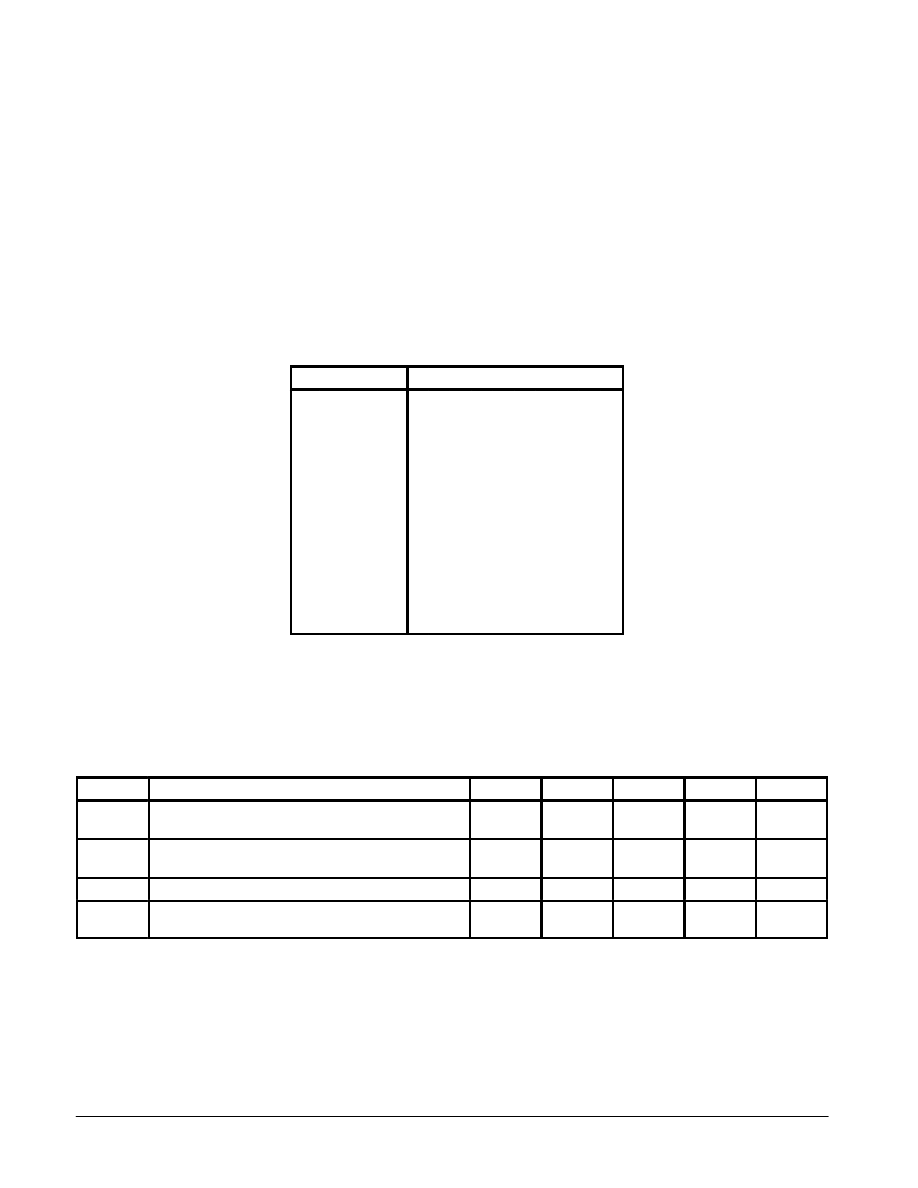
SN54/74LS42
ONE-OF-TEN DECODER
LOW POWER SCHOTTKY
J SUFFIX
CERAMIC
CASE 620-09
N SUFFIX
PLASTIC
CASE 648-08
16
1
16
1
ORDERING INFORMATION
SN54LSXXJ
Ceramic
SN74LSXXN
Plastic
SN74LSXXD
SOIC
16
1
D SUFFIX
SOIC
CASE 751B-03
LOGIC SYMBOL
VCC = PIN 16
GND = PIN 8
15
14
13
12
0 1 2 3 4 5 6 7 8 9
1 2 3 4 5 6 7 9 10 11
A0 A1
A2
A3
5-2
FAST AND LS TTL DATA
SN54/74LS42
FUNCTIONAL DESCRIPTION
The LS42 decoder accepts four active HIGH BCD inputs
and provides ten mutually exclusive active LOW outputs, as
shown by logic symbol or diagram. The active LOW outputs
facilitate addressing other MSI units with LOW input enables.
The logic design of the LS42 ensures that all outputs
are HIGH when binary codes greater than nine are applied
to the inputs.
The most significant input A3 produces a useful inhibit func-
tion when the LS42 is used as a one-of-eight decoder. The A3
input can also be used as the Data input in an 8-output
demultiplexer application.
TRUTH TABLE
A0 A1 A2 A3 0
1
2
3
4
5
6
7
8
9
L
H
L
H
L
H
L
H
L
H
L
H
L
H
L
H
L
L
H
H
L
L
H
H
L
L
H
H
L
L
H
H
L
L
L
L
H
H
H
H
L
L
L
L
H
H
H
H
L
L
L
L
L
L
L
L
H
H
H
H
H
H
H
H
L
H
H
H
H
H
H
H
H
H
H
H
H
H
H
H
H
L
H
H
H
H
H
H
H
H
H
H
H
H
H
H
H
H
L
H
H
H
H
H
H
H
H
H
H
H
H
H
H
H
H
L
H
H
H
H
H
H
H
H
H
H
H
H
H
H
H
H
L
H
H
H
H
H
H
H
H
H
H
H
H
H
H
H
H
L
H
H
H
H
H
H
H
H
H
H
H
H
H
H
H
H
L
H
H
H
H
H
H
H
H
H
H
H
H
H
H
H
H
L
H
H
H
H
H
H
H
H
H
H
H
H
H
H
H
H
L
H
H
H
H
H
H
H
H
H
H
H
H
H
H
H
H
L
H
H
H
H
H
H
H = HIGH Voltage Level
L = LOW Voltage Level
GUARANTEED OPERATING RANGES
Symbol
Parameter
Min
Typ
Max
Unit
VCC
Supply Voltage
54
74
4.5
4.75
5.0
5.0
5.5
5.25
V
TA
Operating Ambient Temperature Range
54
74
– 55
0
25
25
125
70
°
C
IOH
Output Current — High
54, 74
– 0.4
mA
IOL
Output Current — Low
54
74
4.0
8.0
mA
5-3
FAST AND LS TTL DATA
SN54/74LS42
DC CHARACTERISTICS OVER OPERATING TEMPERATURE RANGE
(unless otherwise specified)
S
b l
P
Limits
U i
T
C
di i
Symbol
Parameter
Min
Typ
Max
Unit
Test Conditions
VIH
Input HIGH Voltage
2.0
V
Guaranteed Input HIGH Voltage for
All Inputs
VIL
Input LOW Voltage
54
0.7
V
Guaranteed Input LOW Voltage for
VIL
Input LOW Voltage
74
0.8
V
p
g
All Inputs
VIK
Input Clamp Diode Voltage
– 0.65
– 1.5
V
VCC = MIN, IIN = – 18 mA
VOH
Output HIGH Voltage
54
2.5
3.5
V
VCC = MIN, IOH = MAX, VIN = VIH
VOH
Output HIGH Voltage
74
2.7
3.5
V
CC
, OH
,
IN
IH
or VIL per Truth Table
VOL
Output LOW Voltage
54, 74
0.25
0.4
V
IOL = 4.0 mA
VCC = VCC MIN,
VIN = VIL or VIH
VOL
Output LOW Voltage
74
0.35
0.5
V
IOL = 8.0 mA
VIN = VIL or VIH
per Truth Table
IIH
Input HIGH Current
20
µ
A
VCC = MAX, VIN = 2.7 V
IIH
Input HIGH Current
0.1
mA
VCC = MAX, VIN = 7.0 V
IIL
Input LOW Current
– 0.4
mA
VCC = MAX, VIN = 0.4 V
IOS
Short Circuit Current (Note 1)
– 20
–100
mA
VCC = MAX
ICC
Power Supply Current
13
mA
VCC = MAX
Note 1: Not more than one output should be shorted at a time, nor for more than 1 second.
AC CHARACTERISTICS
(TA = 25
°
C)
S
b l
P
Limits
U i
T
C
di i
Symbol
Parameter
Min
Typ
Max
Unit
Test Conditions
tPLH
tPHL
Propagation Delay
(2 Levels)
15
15
25
25
ns
Figure 2
VCC = 5.0 V
tPLH
tPHL
Propagation Delay
(3 Levels)
20
20
30
30
ns
Figure 1
CC
CL = 15 pF
AC WAVEFORMS
VIN
VOUT
1.3 V
1.3 V
1.3 V
1.3 V
tPHL
tPLH
Figure 1
Figure 2
1.3 V
1.3 V
1.3 V
1.3 V
tPLH
tPHL
VIN
VOUT
Wyszukiwarka
Podobne podstrony:
Marijuana is one of the most discussed and controversial topics around the world
racismz int (2) , Racism has become one of the many burdens amongst multi-cultural worlds like Canad
fitopatologia, Microarrays are one of the new emerging methods in plant virology currently being dev
Język angielski Write a report?out one of the things that you like or?n
One Of Us
Abba One of us
13 One of the most serious problems facing young people today 2
One of us
Next insert your finger in one of the pockets in the square base
Realism, as one of the Grand Theory of International 2
One of us
Abba One of us
One of us (arr by Ulli)
Just One of the Guys Kristan Higgins
Bearden Misc Howard Johnson constructing one of his magnetic motors
One Of Us
The fact is that the World War 2 was one of the cruelest
Garr, Amber Promises Book One of The Syrenka Series
ONE OF THE WORLD S GREATEST WINES guide
więcej podobnych podstron