1
SERVICE MANUAL
SPECIFICATIONS
Dial signal
Tone, 10 PPS (pulse) selectable
Dimensions
Approx. 69
×
74.5
×
225 mm (w/h/d)
(Approx. 2
3/4
×
3
×
8
7/8
inches)
Mass
Approx. 485 g
(Approx. 17 oz), attachments included
Supplied accessories
• Telephone line cords (2)
• Handset cord
Design and specifications are subject to change without notice.
IT-B1
Canadian Model
Central & South America Model
TELEPHONE
MICROFILM
Notes on Chip Component Replacement
•
Never reuse a disconnected chip component.
•
Notice that the minus side of a tantalum capacitor may be dam-
aged by heat.
Photo: WHITE Type
4
4
IT-B1
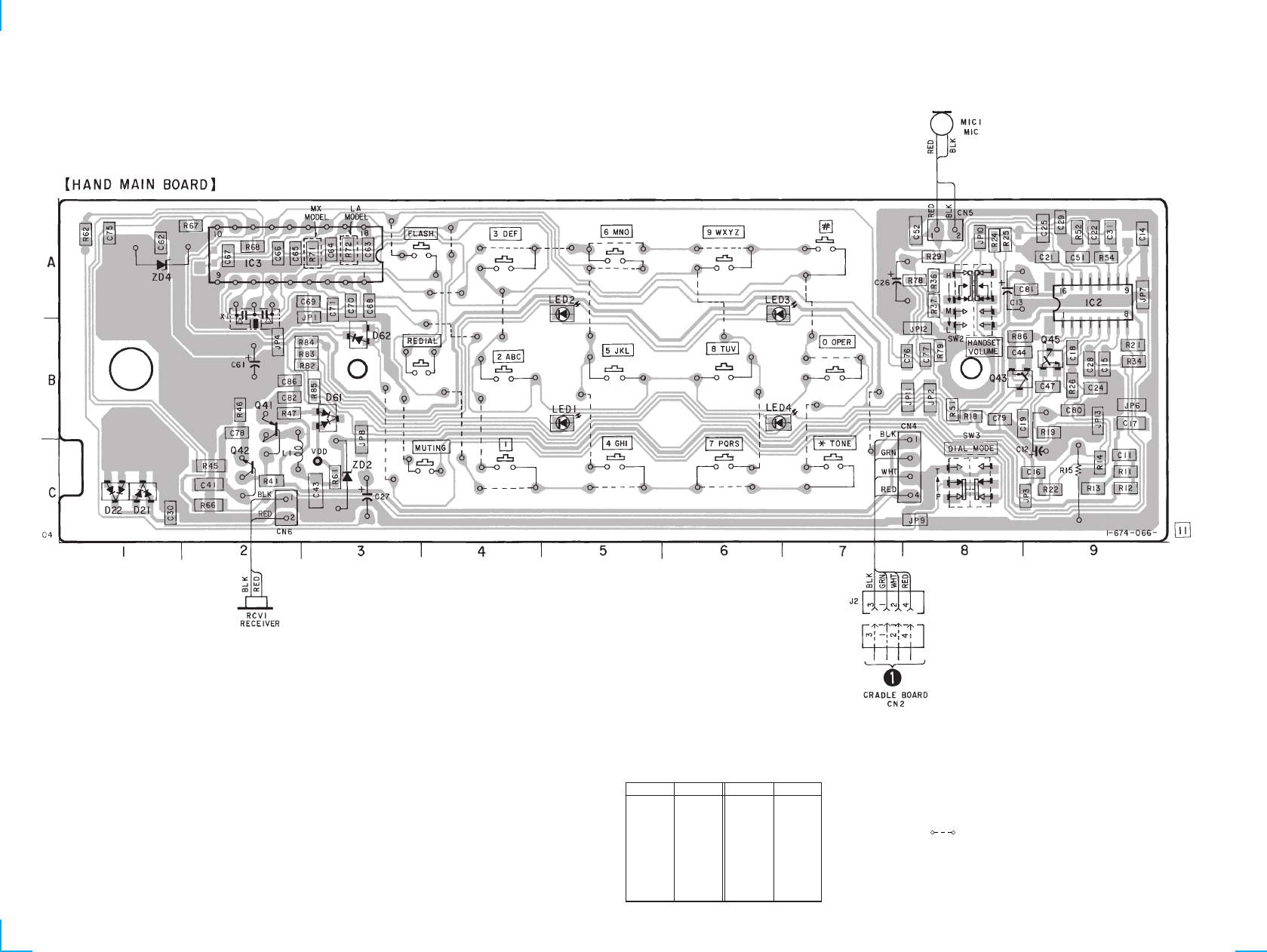
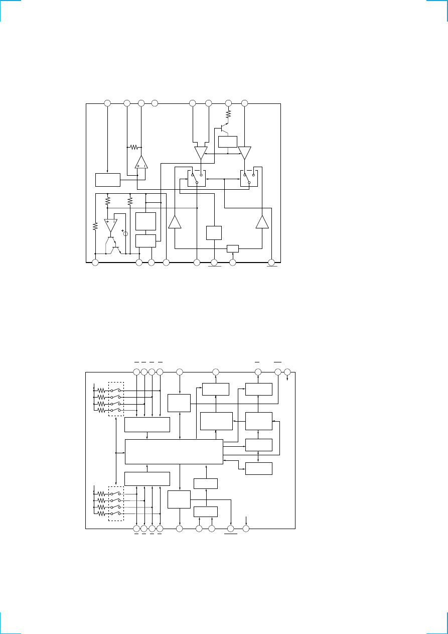
3-1. PRINTED WIRING BOARD — HANDSET SECTION —
SECTION 3
DIAGRAMS
LED3
A-6
LED4
B-6
Q41
B-2
Q42
C-2
Q43
B-8
Q45
B-9
ZD2
C-3
ZD4
A-1
D21
C-1
D22
C-1
D61
B-3
D62
B-3
IC2
A-9
IC3
A-2
LED1
B-5
LED2
A-5
• Semiconductor Location
Ref. No.
Location
Ref. No.
Location
Note:
• X
: parts extracted from the component side.
•
: Carbon pattern.
•
¢
: internal component.
• b
: Pattern from the side which enables seeing.
(The other layer’s patterns are not indicated.)
• Abbreviation
MX
: Mexican model
LA
: Latin American model
5
5
IT-B1
3-2. SCHEMATIC DIAGRAM — HANDSET SECTION — • Refer to page 7 for IC Block Diagrams.
Note:
• All capacitors are in µF unless otherwise noted. pF: µµF
50 WV or less are not indicated except for electrolytics
and tantalums.
• All resistors are in
Ω
and
1
/
4
W or less unless otherwise
specified.
•
%
: indicates tolerance.
•
¢
: internal component.
•
C
: panel designation.
•
U
: B+ Line.
• Connect J2 and J3 with handset cord.
Power voltage is dc 12V and fed with regulated dc power
supply from J3 with 100
Ω
in series.
• Voltage is dc with respect to ground under no-signal
condition.
no mark : OFF HOOK
(
) : ON HOOK
• Voltages are taken with a VOM (Input impedance 10 M
Ω
).
Voltage variations may be noted due to normal produc-
tion tolerances.
• Signal path.
N
: RX (from TEL LINE)
O
: TX (to TEL LINE)
P
: bell
• Abbreviation
MX
: Mexican model
LA
: Latin American model
6
6
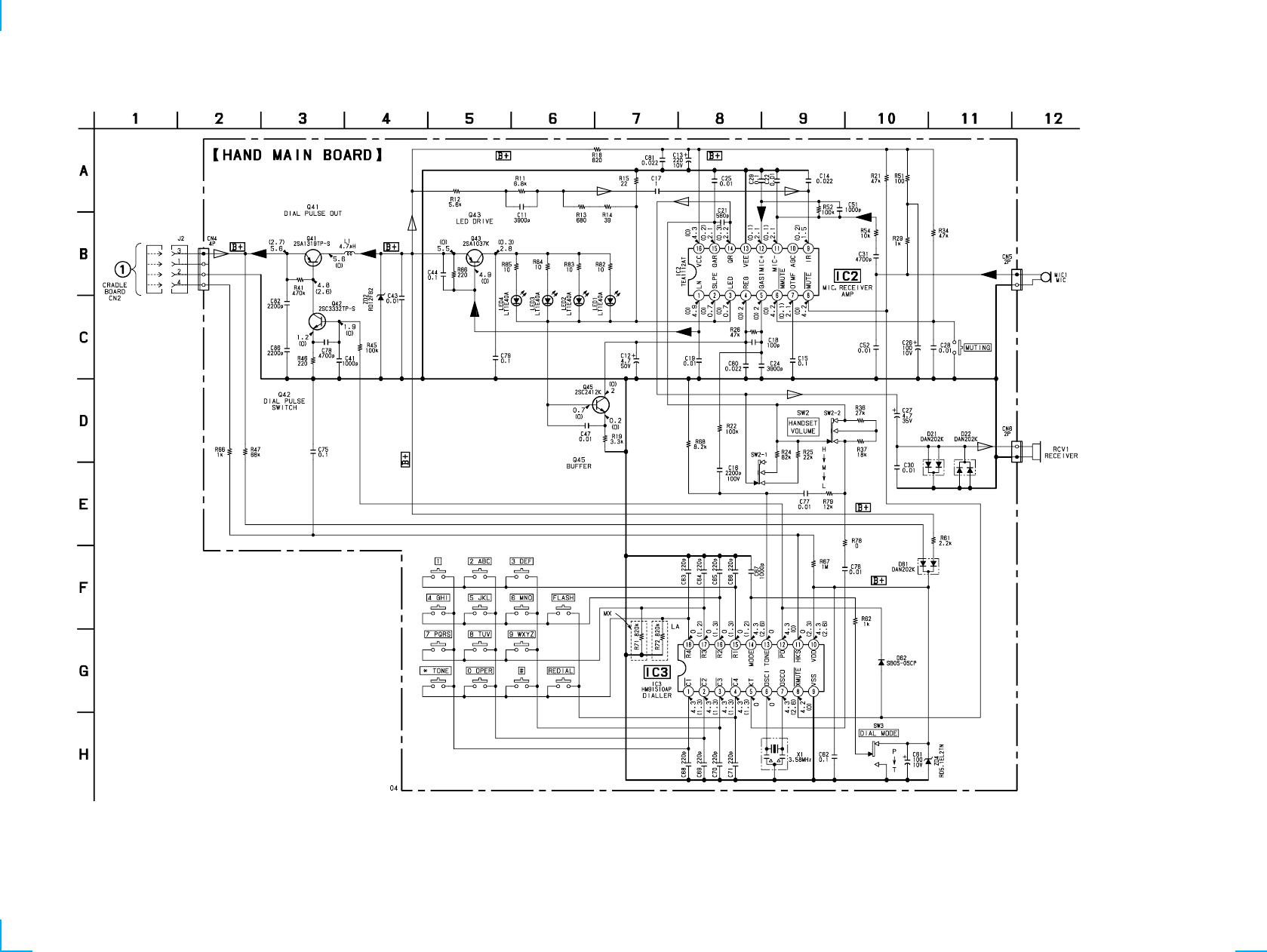
3-4. SCHEMATIC DIAGRAM — CRADLE SECTION —
IT-B1
3-3. PRINTED WIRING BOARD — CRADLE SECTION —
Note:
• All capacitors are in µF unless otherwise noted. pF: µµF
50 WV or less are not indicated except for electrolytics
and tantalums.
• All resistors are in
Ω
and
1
/
4
W or less unless otherwise
specified.
•
%
: indicates tolerance.
•
¢
: internal component.
•
C
: panel designation.
•
U
: B+ Line.
• Power voltage is dc 12V and fed with regulated dc power
supply from J3 with 100
Ω
in series.
• Voltage is dc with respect to ground under no-signal
condition.
no mark : OFF HOOK
(
) : ON HOOK
• Voltages are taken with a VOM (Input impedance 10 M
Ω
).
Voltage variations may be noted due to normal produc-
tion tolerances.
• Signal path.
N
: RX (from TEL LINE)
O
: TX (to TEL LINE)
P
: bell
Note:
• X
: parts extracted from the component side.
•
¢
: internal component.
• b
: Pattern from the side which enables seeing.
(The other layer’s patterns are not indicated.)
D33
D-2
D34
D-1
IC1
B-2
ZD1
B-1
D1
A-3
D2
A-3
D3
A-3
D4
B-3
D5
B-1
D31
C-2
D32
C-1
• Semiconductor Location
Ref. No.
Location
Ref. No.
Location
JW
7
• IC Block Diagrams
IC2 TEA1112AT
IC3 HM91510AP
CURRENT
REFERENCE
LOW
VOLTAGE
CIRCUIT
LED
DRIVER
ATT
MICRO
MUTE
AGC
CIRCUIT
16
VCC
1
LN
2
SLPE
3
LED
4
REG
5
GAS
6
MMUTE
7
OTMF
8
MUTE
GAR
QR
VEE
MIC+
MIC-
IR
AGC
15
14
13
12
11
9
10
ROW
INTERFACE CIRCUIT
COLUMN
INTERFACE CIRCUIT
DIVIDER
OSC
KERNEL CONTROL CIRCUIT
INPUT
INTERFACE
CIRCUIT
OUTPUT
INTERFACE
CIRCUIT
ROW/COLUMN
PROGRAMMING
COUNTER
D/A
CONVERTER
DECODER
&
DATA LATCH
PULSE
GENERATOR
LNB
MEMORY
1
C1
2
C2
3
C3
4
C4
VSS
VDD
5
KT
6
OSCI
7
OSCO
8
XMUTE
9
VSS
18
R4
17
R3
16
R2
15
R1
14
MODE
12
13
TONE
10
VDD
11
HKS
PO
MEMORY
VDD
Wyszukiwarka
Podobne podstrony:
Sony IT B7
Sony IT B9
islcollective worksheets intermediate b1 adult high school speaking time my table what time is it 67
Biznes IT prezentacja
ECCC Sylabus IT M5 D
ITIL v3 Cykl życia usług IT
B1 Klucz do zadan
ECCC Sylabus IT M4 B
ITIL Zarządzanie usługami IT poprzez procesy
ECCC Sylabus IT M5 C
Technologia Informacyjna 22.11.2008, ściągnięte, IT, Technologia Informacyjna(5)
powiklania po znieczuleniu ogolnym, Pielęgniarstwo - materiały na studia, IT
Sony Ericsson GC79, TELEFONIA, Opisy telefonów
Staż IT
anatka Anatomia Wyklady ?it
COMPACT DISK PLAYER MODEL SONY CDX GT212 CDX GT210
B1 Rozumienie tekstu pisanego
więcej podobnych podstron