
5AX
1
TABLE OF CONTENTS
1.
INTRODUCTION
1.1. PREFACE .........................................................................................1-1
1.2. KEY FEATURES ...............................................................................1-1
1.3. PERFORMANCE LIST ......................................................................1-3
1.4. BLOCK DIAGRAM.............................................................................1-4
1.5. INTRODUCE THE PCI - BUS ............................................................1-5
1.6. FEATURES .......................................................................................1-5
1.7. What is AGP .....................................................................................1-6
2.
SPECIFICATION
2.1. HARDWARE .....................................................................................2-1
2.2. SOFTWARE......................................................................................2-2
2.3. ENVIRONMENT ................................................................................2-2
3.
HARDWARE INSTALLATION
3.1. UNPACKING .....................................................................................3-1
3.2. MAINBOARD LAYOUT......................................................................3-2
3.3. QUICK REFERENCE FOR JUMPERS & CONNECTORS ..................3-2
3.4. SRAM INSTALLATION ......................................................................3-4
3.5. DRAM INSTALLATION......................................................................3-5
3.6. CPU INSTALLATION AND JUMPERS SETUP...................................3-5
3.7. CMOS RTC & ISA CFG CMOS SRAM...............................................3-7
3.8. SPEAKER CONNECTOR INSTALLATION.........................................3-7
3.9. ACPI LED CONNECTOR INSTALLATION .........................................3-7

Table of Contents
2
3.10. HARDWARE RESET SWITCH CONNECTOR INSTALLATION........3-7
3.11. GREEN FUNCTION INSTALLATION ...............................................3-7
3.12. PERIPHERAL DEVICE INSTALLATION...........................................3-7
4.
BIOS CONFIGURATION
4.1. ENTERING SETUP………………………………………………………….4-1
4.2. CONTROL KEYS ..............................................................................4-2
4.3. GETTING HELP ................................................................................4-3
4.3.1. Main Menu.....................................................................................4-3
4.3.2. Status Page Setup Menu / Option Page Setup Menu ......................4-3
4.4. THE MAIN MENU ..............................................................................4-3
4.5. STANDARD CMOS SETUP MENU ....................................................4-5
4.6. BIOS FEATURES SETUP .................................................................4-9
4.7. CHIPSET FEATURES SETUP ...........................................................4-13
4.8. POWER MANAGEMENT SETUP ......................................................4-17
4.9. PNP/PCI CONFIGURATION..............................................................4-20
4.10. LOAD BIOS DEFAULTS ..................................................................4-22
4.11. LOAD SETUP DEFAULTS...............................................................4-23
4.12. INTEGRATED PERIPHERALS ........................................................4-24
4.13. SUPERVISOR / USER PASSWORD ...............................................4-30
4.14. IDE HDD AUTO DETECTION ..........................................................4-31
4.15. SAVE & EXIT SETUP ......................................................................4-32
4.16. EXIT WITHOUT SAVING ................................................................4-33
A.Trobuleshooting

5AX
1-1
1. INTRODUCTION
1.1. PREFACE
Welcome to use the 5AX motherboard. The motherboard is a Pipeline 512 KB
CACHE Pentium
Processor based PC / AT compatible system with ISA bus and
PCI Local Bus, and has been designed to be the fastest PC / AT system. There are
some new features allow you to operate the system with the performance you
want.
This manual also explains how to install the motherboard for operation, and how to
set up your CMOS CONFIGURATION with BIOS SETUP program.
1.2. KEY FEATURES
q
Pentium
Processor based PC / AT compatible mainboard with PCI / ISA /
AGP Bus.
q
5 PCI Bus slots, 2 ISA Bus slots, 1 AGP slot.
q
Supports :
•
Pentium
Processor
133 / 166 / 200 MHz ; MMX (166 / 200 / 233),
•
AMD
K6-(166 / 200 / 233 / 266 / 300); K6-2 ( 266 /
300 / 333 / 350 / 380 / 400)
•
Cyrix/IBM
6x86MX ( PR166 / PR200 / PR233 / PR266) ;
M¢ º
-PR300 / PR333
•
IDT
C6-(200 / 225 / 266)
q
Supports true 64 bits CACHE and DRAM access mode.
q
Supports 321 Pins (Socket 7) ZIF white socket on board.
q
Supports 512 KB Pipeline Burst Sync. 2
nd
Level Cache.
q
CPU L1 / L2 Write-Back cache operation.
q
Supports 8 - 768 MB DRAM memory on board.
q
Supports 3*168 pin 64/72 Bit DIMM module.

Introduction
1-2
q
Supports 2-channel Enhanced PCI IDE ports for 4 IDE Devices.
q
Supports 2*COM (16550), 1*LPT (EPP / ECP), 1*1.44MB Floppy port.
q
Supports Green function, Plug & Play function.
q
Licensed AWARD BIOS, FLASH ROM for BIOS update.
q
30.5cm*18.5cm, ATX Form factor.
q
Supports USB port & PS/2 Mouse and K/B port.
q
Supports Keyboard Power On/Off.
q
Supports 3 steps ACPI LED.

5AX
1-3
1.3. PERFORMANCE LIST
The following list of performance data is the testing results of some popular
benchmark testing programs.
These data are just referred by users, and there is no responsibility for different
testing data values gotten by users. (The different Hardware & Software
configuration will result in different benchmark testing results.)
•
CPU
Pentium
Processor MMX-233 MHz , Cyrix 6x86MII-
PR333 , AMD K6-2 400
•
DRAM
(128 × 1) MB SDRAM (LGS GM72N66841CT7J)
•
CACHE SIZE
512 KB
•
DISPLAY
GA-600 (4MB SGRAM)
•
STORAGE
Onboard IDE (IBM DHEA-36481)
•
O.S.
Windows® NT 4.0
•
DRIVER
Display Driver at 1024 x 768 x 256 colors x 75Hz.
ALi Bus Master IDE Driver
Processor
Intel-MMX 233MHz
(66x3.5)
AMD K6-2 400
(100x4)
Cyrix M-II PR333
(83x3)
Winbench98
CPU mark32
465
885
616
FPU Winmark
916
1300
573
Business Disk
1780
1880
1860
Hi-End Disk
4160
4470
4520
Business Graphics
107
168
154
Hi-End Graphics
111
173
172
Winstone98
Business
22.7
31.4
27.8
Hi-End
23.5
32.2
28.6
Introduction
1-4
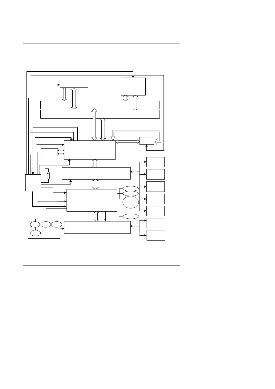
1.4. BLOCK
DIAGRAM
CPU
PBSRAM
AGP
DEVICE
Host
Address
Host Data
Bus
ISA Bus
MD Bus
ALi
M1543C
ALi
M1541
DRAM
MA Bus
100MHz
33MHz
33MHz
33MHz
48MHz
14.318MH
z
PCI
Device
PCI
Device
PCI
Device
PCI
Device
PCI Bus
ISA
Device
ISA
Device
COMA
COMB
LPT
FDD
PS/2
GPIO
USB
100MHz
66MHz
14.318Hz
8MHz
100MHz
14.318Hz
66MHz
Mouse
Keyboard
IDE
DEVICE
66MHz
100MHz
100MHz
ICS9148
AF-75
PCI
Device

5AX
1-5
1.5. INTRODUCE THE PCI - BUS
Connecting devices to a CPU local bus can dramatically increase the speed of I/O-
bound peripherals with only a slight increase in cost over traditional systems.
This price / Performance point has created a vast market potential for local bus
products.
The main barrier to this market has been the lack of an accepted standard for local
bus peripherals.
Many mainboard and chipset manufactures developed their own local bus
implementations, but they are incompatible with each other.
The VL (Video Electronics Standards Association) local bus and PCI (Peripheral
Component Interconnect) bus specification was created to end this confusion.
The PCI - bus standard, under development since Jun. 1992, which is designed to
bring workstation-level performance to standard PC platform. The PCI - bus
removes many of the bottlenecks that have hampered PC for several years.
On the PCI - bus, peripherals operate at the native speed of the computer system,
thus enabling data transfer between peripherals and the system at maximum
speed.
This performance is critical for bandwidth-constrained devices such as video,
multimedia, mass storage, and networking adapters.
PCI - bus standard provides end-users with a low-cost, extendible and portable
local bus design, which will allow system and peripherals from different
manufactures to work together.
1.6. FEATURES
q
32 bits bus transfer mode.
q
Bus Master or Slave access.
q
Memory burst transfer to 132 MB/sec.
q
33 MHz operation speed.
q
10 device loading ability.
q
CPU independent.

Introduction
1-6
1.7. What is AGP
The Accelerated Graphics Port (AGP) is a new port on the Host-To-PCI bridge
device that supports an AGP port. The main purpose of the AGP port is to provide
fast access to system memory.
The AGP port can be used either as fast PCI port (32-bits at 66MHz vs. 32-bits at
33MHz) or as an AGP port which supports 2x data-rate, a read queue, and side
band addressing. When the 2x-data rate is used the port can transmit data at
533Mb/sec (66.6*2*4). The read-queue can be used to pipeline reads – removing
the effects of the reads-latency. Side band addressing can be used to transmit the
data address on a separate line in order to further speed the transaction.

5AX
2-1
2. SPECIFICATION
2.1. HARDWARE
•
CPU
−
Pentium
Processor
133 / 166 / 200 MHz; MMX (166 / 200 / 233)
−
AMD
K6- (166 / 200/ 233 / 266 / 300) ;
K6-2 (266 / 300 / 333 / 350 / 380 / 400)
−
Cyrix/IBM
6x86MX(PR166 / PR200 / PR233 / PR266 );
M¢ º
-PR300 / PR333
−
IDT
C6-(200 / 225 / 266 )
−
321 pins (socket 7) ZIF white socket on board.
−
3.52V / 1.3V-3.5V Dual Power Ready.
•
COPROCESSOR
−
Included in processor.
•
SPEED
−
66 / 75 / 83 / 95 /100MHz system speed.
−
66 MHz AGP-Bus speed.
−
33 MHz PCI-Bus speed.
−
8 MHz AT bus speed.
•
DRAM MEMORY
−
3 banks 168 pins DIMM module socket on board.
−
Use 8 / 16 / 32 / 64 / 128 / 256 MB DIMM module DRAM.
−
8 ~ 768 MB DRAM size.
−
Supports 3.3V SDRAM / EDO type DRAM.
−
Supports ECC or Non-ECC type DRAM.
•
CACHE MEMORY
−
16 / 24 / 32 / 64KB L1cache included in CPU.
−
512 KB 2
nd
Level cache on board.
−
Supports Write Back cache function for both CPU & on
board cache.
•
I/O BUS SLOTS
−
5 xMaster / Slave PCI-BUS Slots.
−
2 x16 bits ISA BUS Slots.
−
1 xAGP Slot.

SPECIFICATION
2-2
•
IDE PORTS
−
2-channel Enhanced IDE port on board.(Using
IRQ14,15)
−
Supports Mode 3,4 IDE & ATAPI CD – ROM.
•
I/O PORTS
−
Supports 2 x16550 COM ports. (Using IRQ4, 3)
−
Supports 1 x EPP/ECP LPT port. (Using IRQ7 or 5 and
DMA3 or 1)
−
Supports 1 x 1.44/2.88 MB Floppy port. (Using DMA2 &
IRQ6)
−
Supports PS/2 Mouse. (Using IRQ12 )
•
GREEN
FUNCTION
−
Suspend mode support.
−
Green switch & ACPI LED support.
−
IDE & Display power down support.
−
Monitor all IRQ / DMA / Display / I/O events.
•
BIOS
−
1Mbit FLASH ROM.
−
Supports Plug & Play Function.
•
DIMENSION
−
ATX Form Factor, 4 layers PCB.
2.2. SOFTWARE
•
BIOS
−
Licensed AWARD BIOS.
−
AT CMOS Setup, BIOS / Chipset Setup, Green
Setup, Hard Disk Utility included.
•
O.S.
−
Operation with MS-DOS
, Windows
95,
Windows
98,WINDOWS
NT, OS/2, NOVELL
and SCO UNIX.
2.3. ENVIRONMENT
•
Ambient Temp.
−
0
°
C to +50
°
C (Operating).
•
Relative Hum.
−
0 to +85% (Operating).
•
Altitude
−
0 to 10,000 feet (Operating).
•
Vibration
−
0 to 1,000 Hz.
•
Electricity
−
4.9 V to 5.2 V.
−
Max. 20A current at 5V.

5AX
3-1
3. HARDWARE INSTALLATION
3.1. UNPACKING
The mainboard package should contain the following:
•
The 5AX mainboard.
•
USER’S MANUAL for mainboard.
•
Cable set for IDE ¡ B
Floppy.
•
Diskette or CD for Mainboard Utility.
The mainboard contains sensitive electric components which can be easily
damaged by static electricity, so the mainboard should be left in its original packing
until it is installed.
Unpacking and installation should be done on a grounded anti-static mat.
The operator should be wearing an anti static wristband, grounded at the same
point as the anti-static mat.
Inspect the mainboard carton for obvious damage. Shipping and handling may
cause damage to your board. Be sure there are no shipping and handling damage
on the board before proceeding.
After opening the mainboard carton, extract the system board and place it only on
a grounded anti-static surface component side up. Again inspect the board for
damage.
Press down on all of the socket IC’s to make sure that they are properly seated. Do
this only on with the board placed on a firm flat surface.
M
DO NOT APPLY POWER TO THE BOARD IF IT HAS BEEN DAMAGED.
It is assumed that the chassis is designed for a standard ATX mainboard mounting.
Place the chassis on the anti-static mat and remove the cover.
Take the plastic clips, Nylon stand-off and screws for mounting the system board,
and keep them separate.

HARDWARE INSTALLATION
3-2
3.2. MAINBOARD LAYOUT
CPU
SW
JP3
1
BANK 0
BANK 2
BANK 1
IDE 2
IDE 1
FLOPPY
LPT
COM A
PS/2
USB
COM B
PCI 1
PCI 2
PCI 3
PCI 4
SL 3
SL 5
SL 4
SL 6
ATX POWER
AGP
FAN
PWR
JP8 JP7
JP9
1
1
M1541
M1543C
BAT1
5AX
JP10
BIOS
PCI 5
×Figure 3.1Ø
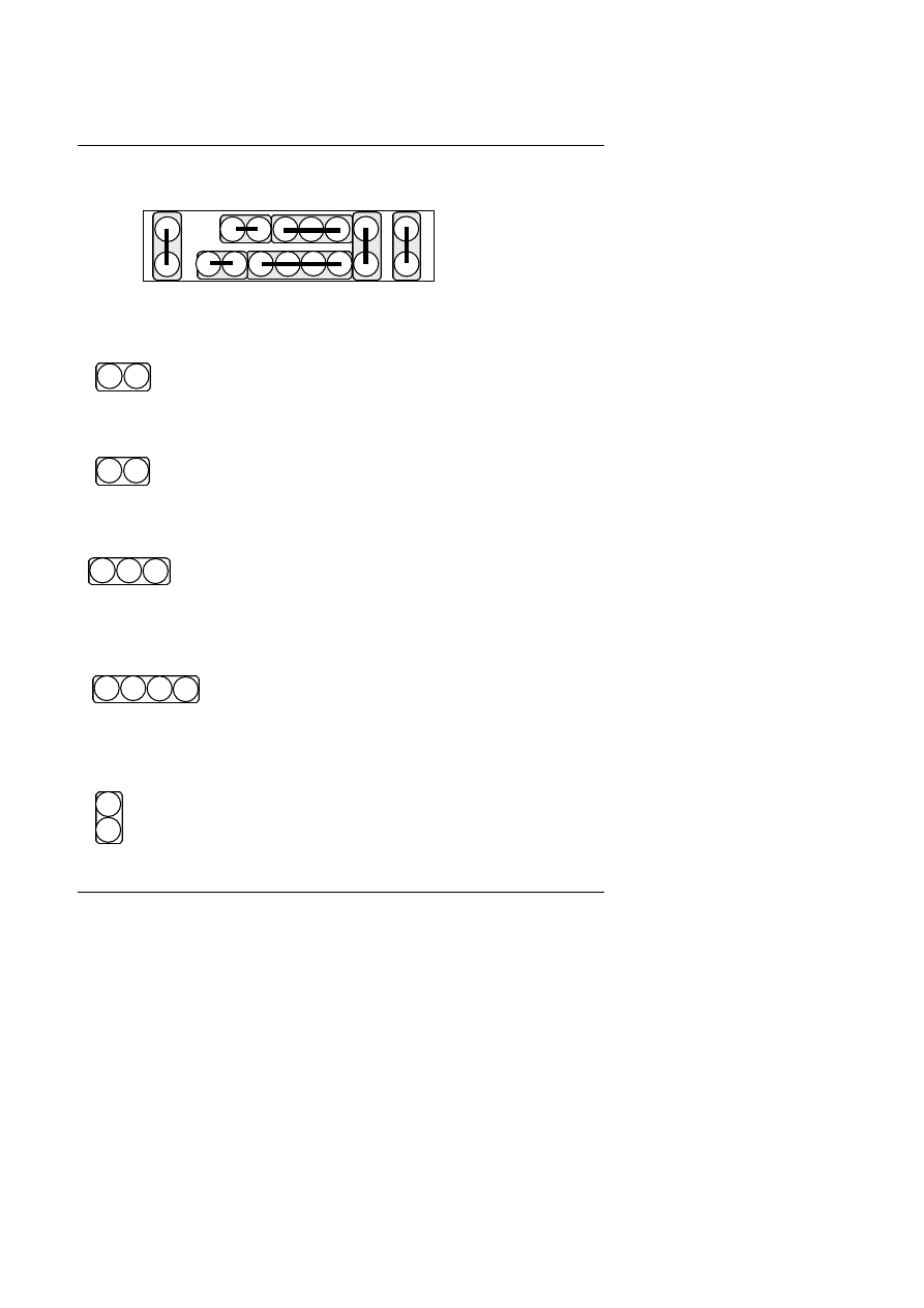
3.3. QUICK REFERENCE FOR JUMPERS & CONNECTORS
t
I/O Port Connectors
IDE 1
For Primary IDE port.
IDE 2
For Secondary IDE port.
FLOPPY
For Floppy port.
USB
For USB port.
COM B
For Serial port2 (COM B){Support Modem Ring On}.
COM A
For Serial port1 (COM A){Support Modem Ring On}.
LPT
For LPT port.
PS/2
For PS/2 Mouse & Keyboard Connector.
ATX PWR
For ATX Power Connector.
5AX
3-3
JP6 : 2*11 PIN Jumper
PWR: Soft Power Connector
RES:Reset Switch
Open: Normal Operation
Short: For Hardware Reset System
P+P
−
P
−
: Power LED
PIN 1: anode (+)
PIN 2: cathode (
−
)
PIN 3: cathode (
−
)
SPKR: Speaker Connector
PIN 1: VCC
PIN 2: NC
PIN 3: NC
PIN 4: Data
HD: IDE Hard Disk Active LED
PIN 1: LED anode (+)
PIN 2: LED cathode (
−
)
1
1
1
PWR P+P
−
P
−
HD
RES
SPKR
JP6
1
1
1
+
−
GN
GD
On – Off : For POWER ON or Suspend IN / OUT.
On 4 sec : For POWER OFF before VGA Enable or CMOS
setup select “ delay 4sec.” for POWER OFF
mode.
HARDWARE INSTALLATION
3-4
GN: Green Switch
Open: Normal operation
Short: Entering Green Mode
GD: Green Function Active LED
PIN 1: LED athode (+)
PIN 2: LED cathode (
−
)
t
JP5: Wake on Lan
Pin No.
Function
1
+5V SB
2
GND
3
Signal
t
FAN PWR: CPU cooling FAN Power Connector
Pin No.
Function
1
GND.
2
+12V
3
NC
t
JP3: Keyboard Power On/Off Connector
Pin No.
Function
1,2 Close
Enabled Keyboard power on.
2,3 Close
Disabled Keyboard power on. (Default)
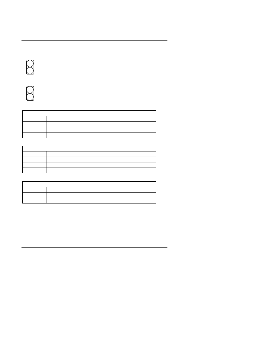
3.4. SRAM INSTALLATION
Sync. SRAM (Pipeline Burst SRAM)
If Sync SRAM Chip is installed, it consists of Pipeline Burst 1 Pc 64 K x 64
512KByte.
1
1

5AX
3-5
3.5. DRAM INSTALLATION
The mainboard can be installed with 8 / 16 / 32 / 64 / 128 / 256 MB 168 pins DIMM
module DRAM, and the DRAM speed must be 67~100 MHz for SDRAM. The
DRAM memory system on mainboard consists of bank 0, 1 & bank 2.
Because the 168 pins DIMM module is 64 bits width, using 1 PCS which can match
a 64 bits system. The total memory size is 8 MB ~ 768 MB DRAM. The DRAM
installation position refer to Figure 3.1, and notice the Pin 1 of DIMM module must
match with the Pin 1 of DIMM socket. Insert the DRAM DIMM module into the
DIMM socket at Vertical angle. If there is a wrong direction of Pin 1, the DRAM
DIMM module couldn't be inserted into socket completely
.
3.6. CPU INSTALLATION AND JUMPERS SETUP
The system speed depends on the frequency of Clock Generator. The user can
change SW selection to set up the system speed to 66 / 75 / 83 / 95 /100MHz for
3.3V/2.5V Pentium
Processor 133 / 166 / 200 MHz; MMX (166 / 200 / 233), AMD
K6-(166 / 200/ 233 / 266 / 300) ; K6-2 ( 266 / 300 / 333 / 350 / 380 / 400);
Cyrix/IBM 6x86MX (PR166 / PR200 / PR233 / PR266 ); M¢ º
-PR300/ PR333 ;
IDT C6-(200 / 225 / 266).
The mainboard can use Pentium
Processor, MMX, AMD-K6, AMD-K6-2,
Cyrix / IBM 6x86MX , Cyrix M¢ º
, IDT C6 CPU, and the CPU speed must match
with the frequency of Clock generator. It will cause system hanging up if the Clock
generator frequency is faster than CPU's.
M
The CPU is a sensitive electric component and it can be easily damaged
by static electricity, so users must keep it away from metal surface when
the CPU is installed onto mainboard.
M
When the user installs the CPU on socket, please notice that the PIN 1 of
CPU is in the same corner as the PIN 1 of socket!
M
Before the CPU is installed, the mainboard must be placed on a flat
plane in order to avoid being broken by the pressure of CPU installation.
HARDWARE INSTALLATION
3-6
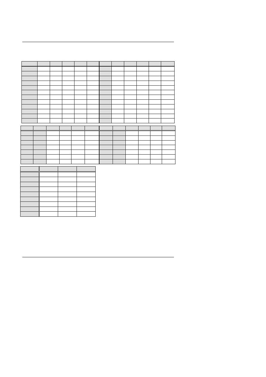
SW: CPU INT./ EXT. FREQ. RATIO
O: ON
X: OFF
SW
4
5
6
7
8
SW
4
5
6
7
8
1.3V
X
X
X
X
O
2.5V
O
X
O
X
X
1.4V
X
O
X
X
O
2.6V
X
O
O
X
X
1.5V
X
X
O
X
O
2.7V
O
O
O
X
X
1.6V
X
O
O
X
O
2.8V
X
X
X
O
X
1.7V
X
X
X
O
O
2.9V
O
X
X
O
X
1.8V
X
O
X
O
O
3.0V
X
O
X
O
X
1.9V
X
X
O
O
O
3.1V
O
O
X
O
X
2.0V
X
O
O
O
O
3.2V
X
X
O
O
X
2.1V
O
X
X
X
X
3.3V
O
X
O
O
X
2.2V
X
O
X
X
X
3.4V
X
O
O
O
X
2.3V
O
O
X
X
X
3.5V
O
O
O
O
X
2.4V
X
X
O
X
X
---
---
---
---
---
---
CPU
AGP
JP7
JP8
JP9
JP10
CPU
AGP
JP7
JP8
JP9
JP10
66
66
2-3
2-3
2-3
1-2
110
73
1-2
1-2
1-2
2-3
75
60
1-2
2-3
2-3
2-3
115
77
1-2
2-3
1-2
1-2
75
75
2-3
1-2
2-3
1-2
120
80
1-2
2-3
1-2
2-3
83
66
1-2
2-3
2-3
1-2
125
41
2-3
1-2
1-2
1-2
95
63
1-2
1-2
2-3
2-3
130
43
2-3
1-2
1-2
2-3
100
66
1-2
1-2
2-3
1-2
135
45
2-3
2-3
1-2
1-2
105
70
1-2
1-2
1-2
1-2
140
47
2-3
2-3
1-2
2-3
SW
1
2
3
X1.5
X
X
X
X2
O
X
X
X2.5
O
O
X
X3
X
O
X
X3.5
X
X
X
X4
O
X
O
X4.5
O
O
O
X5
X
O
O
X5.5
X
X
O
«Note: We don’t recommend you to setup your system speed to 105 , 110 , 115 ,
120 , 125 , 130 , 135 or 140 MHz because these frequencies are not the
standard specifications for CPU, Chipset and most of the peripherals.
Whether your system can run under 105, 110, 115,120, 125, 130, 135 or
140 MHz properly will depend on your hardware configurations: CPU,
SDRAM, Cards, etc.

5AX
3-7
3.7. CMOS RTC & ISA CFG CMOS SRAM
Built-in Real Time Clock (RTC) With 256B CMOS SRAM in M5819.
3.8. SPEAKER CONNECTOR INSTALLATION
There is a speaker in AT system for sound purpose. The 4 - Pins connector SPKR
is used to connect speaker. The speaker can work well in both direction of
connector when it is installed to the connector SPKR on mainboard.
3.9. ACPI LED CONNECTOR INSTALLATION
This mainboard uses the existing power LED as ACPI LED .The ACPI LED will
light on when system is power-on .The ACPI LED is off when the system is power-
off. The ACPI LED will blink when system is in Green mode.This connector should
be installed to ACPI LED jumper of the mainboard in correct direction.
3.10. HARDWARE RESET SWITCH CONNECTOR INSTALLATION
The RESET switch on panel provides users with HARDWARE RESET function
which is almost the same as power-on/off. The system will do a cold start after the
RESET switch is pushed and released by user. The RESET switch is a 2 PIN
connector and should be installed to RES on mainboard.
3.11. GREEN FUNCTION INSTALLATION
There is one jumper for the purpose of power saving, GN, to indicate the power
saving function . This mainboard uses the existing power LED as ACPI LED . If the
ACPI LED is blinking, the system is in green mode. The GN switch will force the
system into green mode .
3.12. PERIPHERAL DEVICE INSTALLATION
After installation of the device and setup of the jumpers, the mainboard can be
mounted into the case and fixed by screw. To complete the mainboard installation,
the peripheral devices could be installed now. The basic system needs a display
interface card and a storage device.
If a PCI - Bus device is to be installed in the system, any one of three PCI - Bus
slots can be used for Slave or Master PCI - Bus device.
After installing the peripheral device, the user should check everything again and
prepare to power-on the system.

Wyszukiwarka
Podobne podstrony:
motherboard manual sata raid os nforce3 e
motherboard manual sata raid os via8237 e
BE6 II Motherboard User’s Manual
PANsound manual
als manual RZ5IUSXZX237ENPGWFIN Nieznany
hplj 5p 6p service manual vhnlwmi5rxab6ao6bivsrdhllvztpnnomgxi2ma vhnlwmi5rxab6ao6bivsrdhllvztpnnomg
BSAVA Manual of Rabbit Surgery Dentistry and Imaging
Okidata Okipage 14e Parts Manual
Bmw 01 94 Business Mid Radio Owners Manual
Manual Acer TravelMate 2430 US EN
manual mechanika 2 2 id 279133 Nieznany
4 Steyr Operation and Maintenance Manual 8th edition Feb 08
Oberheim Prommer Service Manual
cas test platform user manual
Kyocera FS 1010 Parts Manual
juki DDL 5550 DDL 8500 DDL 8700 manual
Forex Online Manual For Successful Trading
ManualHandlingStandingAssessment
więcej podobnych podstron