AVR042: AVR Hardware Design Considerations
Features
• Providing robust supply voltage, digital and analog.
• Connection of RESET line.
• SPI interface for In-System Programming.
• Using external crystal or ceramic resonator oscillators.
1 Introduction
This application note has been written to provide answers to some of the questions
and problems faced when starting designs involving AVR microcontrollers. The
application note treats topics that are known to cause problems. The scope is to
provide an introduction to potential design problems rather than being an
exhaustive walk-through of how to design applications using the AVR
microcontrollers. This document is thus a collection of information from existing
Atmel AVR documents, combined with information that is not previously
documented.
8-bit
Microcontrollers
Application Note
Rev. 2521F-AVR-04/08
It is highly recommended to read the application note AVR040 - “EMC Design
Considerations” – before initiating a new design, especially if the aim of the design
is a commercial application that needs to meet the requirements of the EMC
directive (or similar directives in countries outside Europe). The application note is
available from the AVR section of the official Atmel website
2
AVR042
2 Power Supply
Two aspects should be considered when designing the power supply for the
discrete/digital elements of an AVR; ESD protection and noise emission. Both these
topics are treated in details in the AVR040 application note, and only a short
summary is included in this document.
2.1 Digital supply
Looking at the datasheet for an AVR microcontroller, one can be fooled to believe that
power supply is not critical. The device has a very wide voltage range, and draws only
a few mA supply current. But as with all digital circuits, the supply current is an
average value. The current is drawn in very short spikes on the clock edges, and if
I/O lines are switching, the spikes will be even higher. The current pulses on the
power supply lines can be several hundred mA if all eight I/O lines of an I/O port
changes value at the same time. If the I/O lines are not loaded, the pulse will only be
a few ns.
This kind of current spike cannot be delivered over long power supply lines; the main
source is (or should be) the decoupling capacitor.
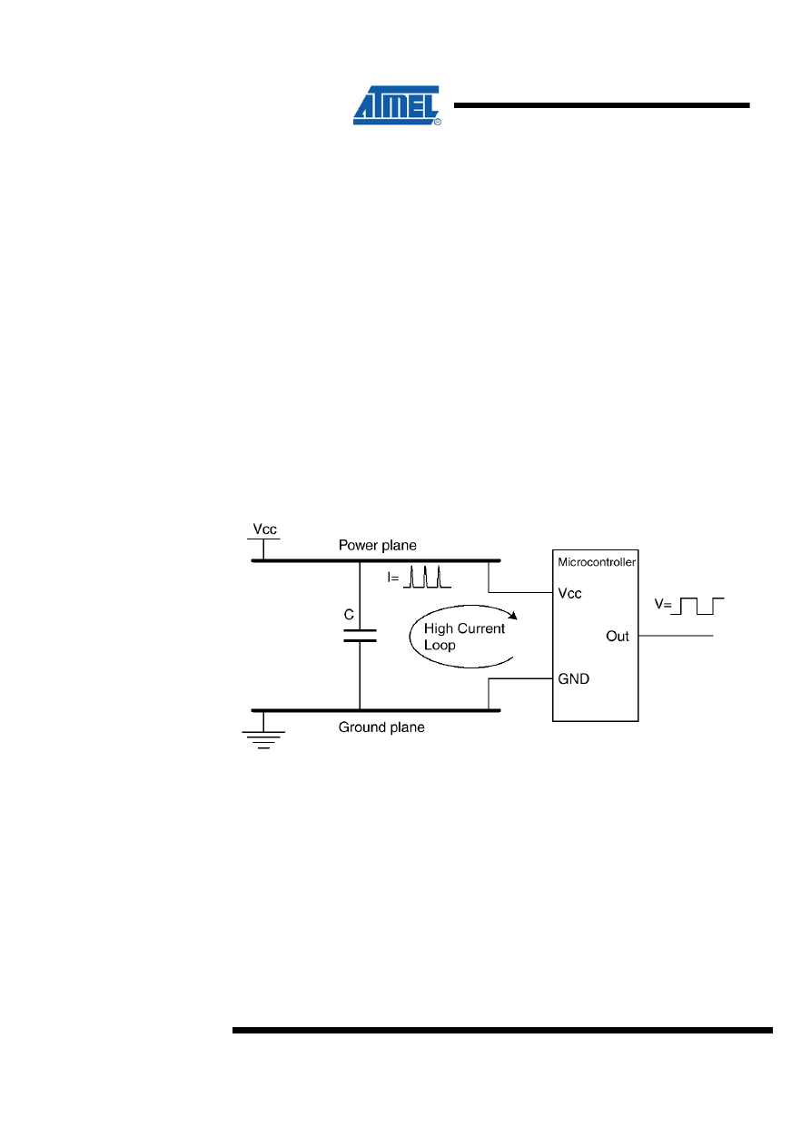
Figure 2-1. Incorrect decoupling
Figure 2-1 shows an example of insufficient decoupling. The capacitor is placed too
far away from the microcontroller, creating a large high current loop. The power and
ground planes here are parts of the high current loop. As a result of this, noise is
spread more easily to other devices on the board, and radiated emission from the
board is increased even further. The whole ground plane will act as an antenna for
the noise, instead of only the high current loop. This will be the case if the power and
ground pins are connected directly to the planes (typical for hole-mounted
components) and the decoupling capacitor is connected the same way. The same is
often seen for boards with surface-mount components if the integrated circuits are
placed on one side of the board and the decoupling capacitors are placed on the
other.
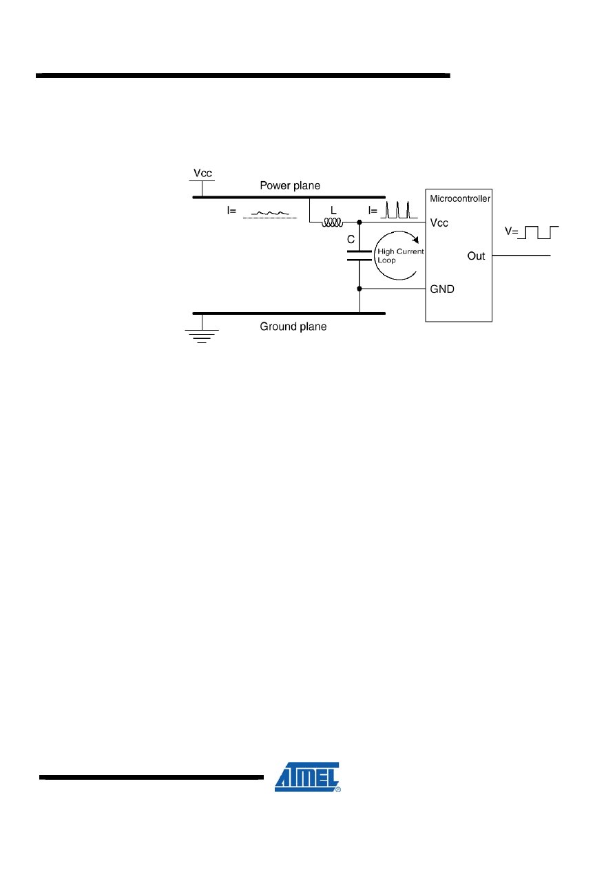
Figure 2-2 shows a better placement of the capacitor. The lines that are part of the
high current loop are not part of the power or ground planes. This is important, as the
power and ground planes otherwise will spread a lot of noise. Further, the figure
2521F-AVR-04/08
AVR042
shows another improvement of the decoupling. A series inductor is inserted to reduce
the switching noise on the power plane. The series resistance of the inductor must of
course be low enough to ensure that there will be no significant DC voltage drop.
Figure 2-2. Decoupling with series inductor.
Generally, the AVR devices where power and ground lines are placed close together
(like the ATmega8535) will get better decoupling than devices with industry standard
pin-out (like the ATmega8515), where the power and ground pins are placed in
opposite corners of the DIP package. This disadvantage can be overcome by using
for example a TQFP package, which allows decoupling capacitors to be placed very
close to the die. For devices with multiple pairs of power and ground pins, it is
essential that every pair of pins get its own decoupling capacitor.
The main supply should also have a tantalum capacitor of some
μF to stabilize it.
2.2 Analog supply
The AVR devices that have built-in ADC have a separate analog supply voltage pin,
AVcc. This separate voltage supply is provided to make the analog circuits less prone
to the digital noise originating from the switching of the digital circuits.
To be able to obtain good accuracy with the ADC the analog supply voltage must be
decoupled separately, in the same manner as the digital supply voltage. If a separate
analog ground (AGND) is present, the analog ground should be separated from the
digital ground, - so that the analog and digital ground are only connected at one point,
- the origin of the GND i.e. at the power supply GND.
3 Connection of RESET pin on AVRs
The RESET pin on the AVR is active LOW, and setting the pin LOW externally will
thus result in a reset of the AVR. The RESET has two purposes:
1. To release all lines by tri-stating all pins (except XTAL pins), initialize all I/O
registers and set program counter to zero.
2. To enter programming mode (for some parts also the PEN line is used to enter
programming mode). Furthermore it is possible to enter high-voltage/parallel
programming mode by drawing the RESET pin “very” high, where very high means
11.5 – 12.5V (refer to the datasheet of the device for more information).
3
2521F-AVR-04/08
4
AVR042
The reset line has an internal pull-up resistor, but if the environment is noisy it can be
insufficient and reset can therefore occur sporadically. Refer to datasheet for value of
pull-up resistor on specific devices.
Different approaches can be used to connect the RESET pin so that unintentional
reset of the AVR is avoided. External brown-out or supervisory circuit can be used to
control the RESET pin. If an external brown-out circuit, like the ones described in
application note AVR180, is applied one would not need to consider how to connect
the RESET pin further. However, if the AVR device used in the application has built-in
brown-out circuit, the external brown-out can be saved and a more simple solution
can be chosen to control the state of the RESET pin.
Connecting the RESET so that it is possible to enter both high-voltage programming
and ordinary low level reset can be achieved by applying a pull-up resistor to the
RESET line. This pull-up resistor makes sure that reset does not go low unintended.
The pull-up resistor can in theory be of any size, but if the AVR should be
programmed from e.g. STK500/AVRISP the pull-up should not be so strong that the
programmer cannot activate RESET by draw the RESET line low. The recommended
pull-up resistor is 4.7kOhm or larger when using STK500 for programming. For
debugWIRE to function properly, the pull-up must not be smaller than 10kOhm.
To protect the RESET line further from noise, it is an advantage to connect a
capacitor from the RESET pin to ground. This is not directly required since the AVR
internally have a low-pass filter to eliminate spikes and noise that could cause reset.
Applying an extra capacitor is thus an additional protection. However, note that this
capacitor cannot be present if debugWIRE is used.
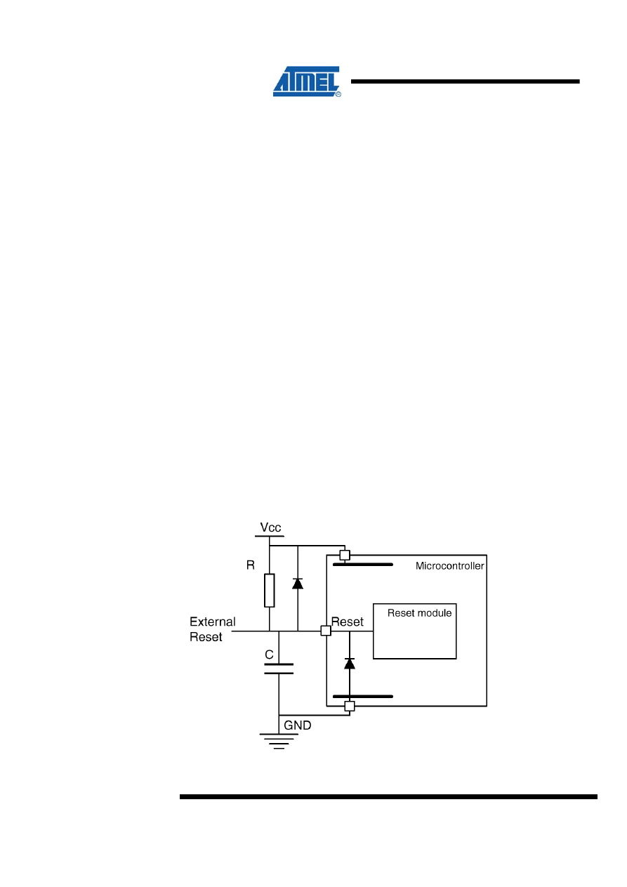
If not using High Voltage Programming it is recommended to add an ESD protecting
diode from RESET to Vcc, since this is not internally provided due to High Voltage
Programming. The components should be located physically close to the RESET pin
of the AVR. Figure 3-1 shows the recommended circuit on the RESET line.
Figure 3-1. Recommended Reset Pin connection.
2521F-AVR-04/08
AVR042
4 Connecting ISP lines
The In-System Programmable (ISP) lines are used for programming the Flash,
EEPROM, Lock-bits and most Fuse-bits in all AVRs (except the ATtiny11 and
ATtiny28). This feature makes it possible to program the AVR on the last stage of
production of a target application board, reprogram if SW bugs are identified late in
the process, or even update the AVR in the field if required. It is therefore highly
recommended to always design the target application board so that the ISP
connectors can be accessed in some way, - just in case.
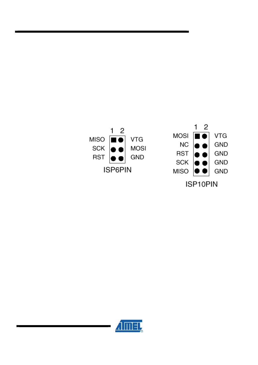
Two standard connectors are provided by the Atmel ISP programmers; A 6 pin and a
10 pin connector. These are seen in Figure 4-1. In addition to the data lines (MOSI
and MISO) and the bus clock (SCK), target voltage VTG, GND and RESET (RST)
are provided through these connectors.
Figure 4-1. Standard ISP connectors on STK500, AVR ISP and STK200/STK300
Some ISP programmers are supplied by the target power supply. In this way they
easily adapt to the correct voltage level of the target board. Other ISP programmers,
like STK500, can alternatively power the target board via the VTG line. In that case it
is important that the power supply on the target is not switched on. Read the User
Guide of the ISP programmer to find out what capabilities your programmer has and
what kind of physical interface it has.
The ISP lines are on most devices located at the same pins as the Peripheral Serial
Interface (SPI), or else on pins that can be used for other purposes. Consult the
device data sheet to find out which lines are used for ISP. In case other devices than
the AVR is connected to the ISP lines the programmer must be protected from any
device, other than the AVR, that may try to drive the lines. This is especially important
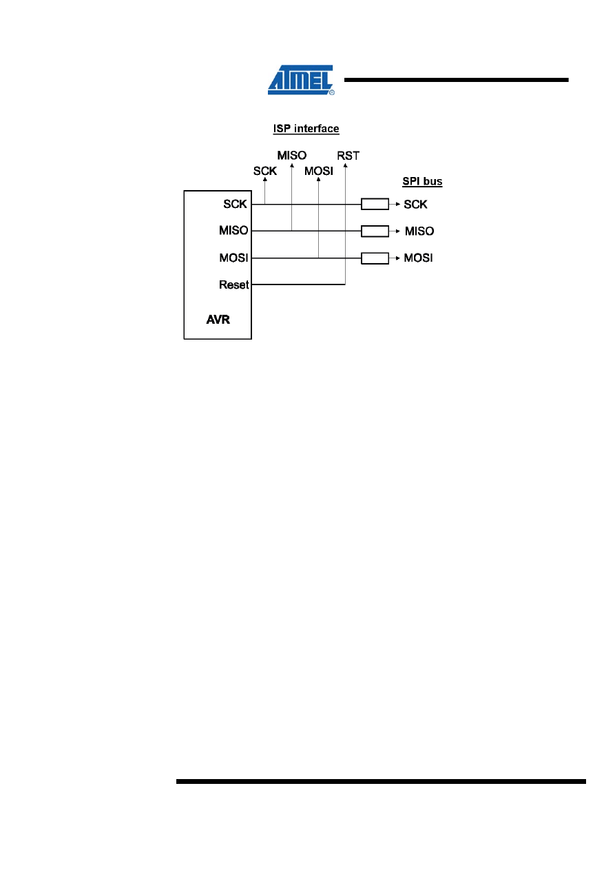
with the SPI bus, as it is similar to the ISP interface. Applying series resistors on the
SPI lines, as depicted in Figure 4-2, is the easiest way of doing this. The AVR will
never drive the SPI lines in a programming situation, since the AVR is held in RESET
to enter programming mode – and RESET’ing the AVR tri-states all pins.
5
2521F-AVR-04/08
6
AVR042
Figure 4-2. Connecting the SPI to the ISP interface.
Multiple AVRs in a single application can share the same ISP interface to make it
possible to program all of the devices through a minimal interface. However, the AVR
devices will all respond to the ISP instructions if special design considerations are not
made. If it is desired to have only one ISP interface on the target board, the ISP
programming can be designed so that only one of the AVR devices is provided with a
SPI clock at a time. All other SPI lines can then be shared. In this way all AVRs can
be located “behind” the same protection resistors, since they all are held in RESET
while the ISP reset line is activated. The gating of the ISP clock can be accomplished
e.g. using jumpers. Alternatively, a solution is to have multiple ISP interfaces, one for
each device, all protected as shown in Figure 4-2.
5 Using crystal and ceramic resonators
Most AVR MCUs can use different clock sources. The optional external clock sources
are Clock, RC oscillator, crystal or ceramic resonator. The use of crystals and
ceramic resonators are in some designs causing problems due to the fact that the use
of these clock sources are not well understood. This section therefore treats the topic
of using crystals and ceramic resonators in relation to AVR MCUs. The description
focus on features and parameters relevant for designing applications where crystals
or ceramic resonators are used rather than trying to be a complete description of the
theory related to the topic.
5.1 Selecting the clock source in the AVR
The clock source used by the AVR is selected through the fuses. Most ISP and
parallel programmers can program the fuses that are related to selecting a clock
source. The fuses are not erased when the AVR memory is erased and the fuses
therefore only require to be programmed if the fuse settings should be altered.
Programming the fuses each time the device is erased and reprogrammed is thus not
necessary. The clock options that are relevant for this document are:
• “Ext. low-frequency crystal”
• “Ext. crystal oscillator”
2521F-AVR-04/08
AVR042
7
2521F-AVR-04/08
• “Ext. ceramic resonator”
Several sub-settings relating to the start-up time of the AVR can be selected, but the
3 clock options mentioned are the fundamental settings that should be focused on.
The clock options available can vary between AVR devices, - not all devices have the
ability to run on various external oscillators. Check the datasheet for the relevant
device to determine the clock options.
One should be aware that if selecting a different clock source than is actually applied,
the AVR might not run since different oscillator circuits are activated internally in the
AVR dependent on the selected clock option. Since the fuses are not cleared by a
memory erase, it can cause problems if incorrect settings are chosen.
5.2 General about crystals and ceramic resonators
The typical type of crystal used for the AVR is the AT-cut parallel resonant crystal.
The ceramic resonator is very similar to the AT-cut parallel resonant crystal, but is so
to say a low cost, low quality version of the crystal. The ceramic resonator has a
lower Q-value, which is both an advantage and disadvantage. Due to the lower Q-
value the oscillator frequency of the ceramic resonator can more easily be “tuned” to
a desired frequency, but is also more sensitive to temperature and load changes,
causing undesired frequency variations. The advantage of the ceramic resonators is
that it has a faster start-up than crystals.
In general there will not be distinguished between crystals and ceramic resonators in
this section and the term “resonator” will thus refer to both devices.
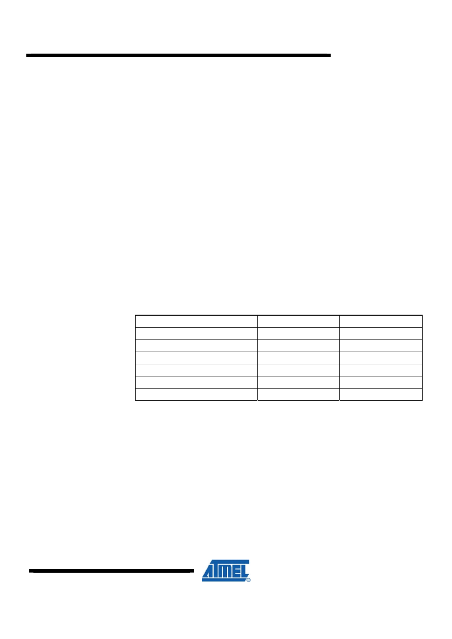
Table 5-1. Technical differences between ceramic resonators and quarts crystal
Ceramic resonator
Quartz crystal
Aging
±3000 ppm
± 10 ppm
Frequency tolerance
± 2000-5000 ppm
± 20 ppm
Freq. temperature characteristics
± 20-50 ppm/˚C
± 0.5 ppm/˚C
Frequency pullability
± 100-350 ppm/pF
± 15 ppm/pF
Oscillator rise time
0.01-0.5 ms
1-10 ms
Quality factor (Qm)
100-5000
10
3
-5·10
5
The parallel resonator is intended used in circuits, which contains reactive
components, usual capacitors. Such circuits depend on the combination of the
reactive components and the resonator to accomplish the phase shift necessary to
start and maintain the oscillation at a given frequency. Basic oscillator circuits used
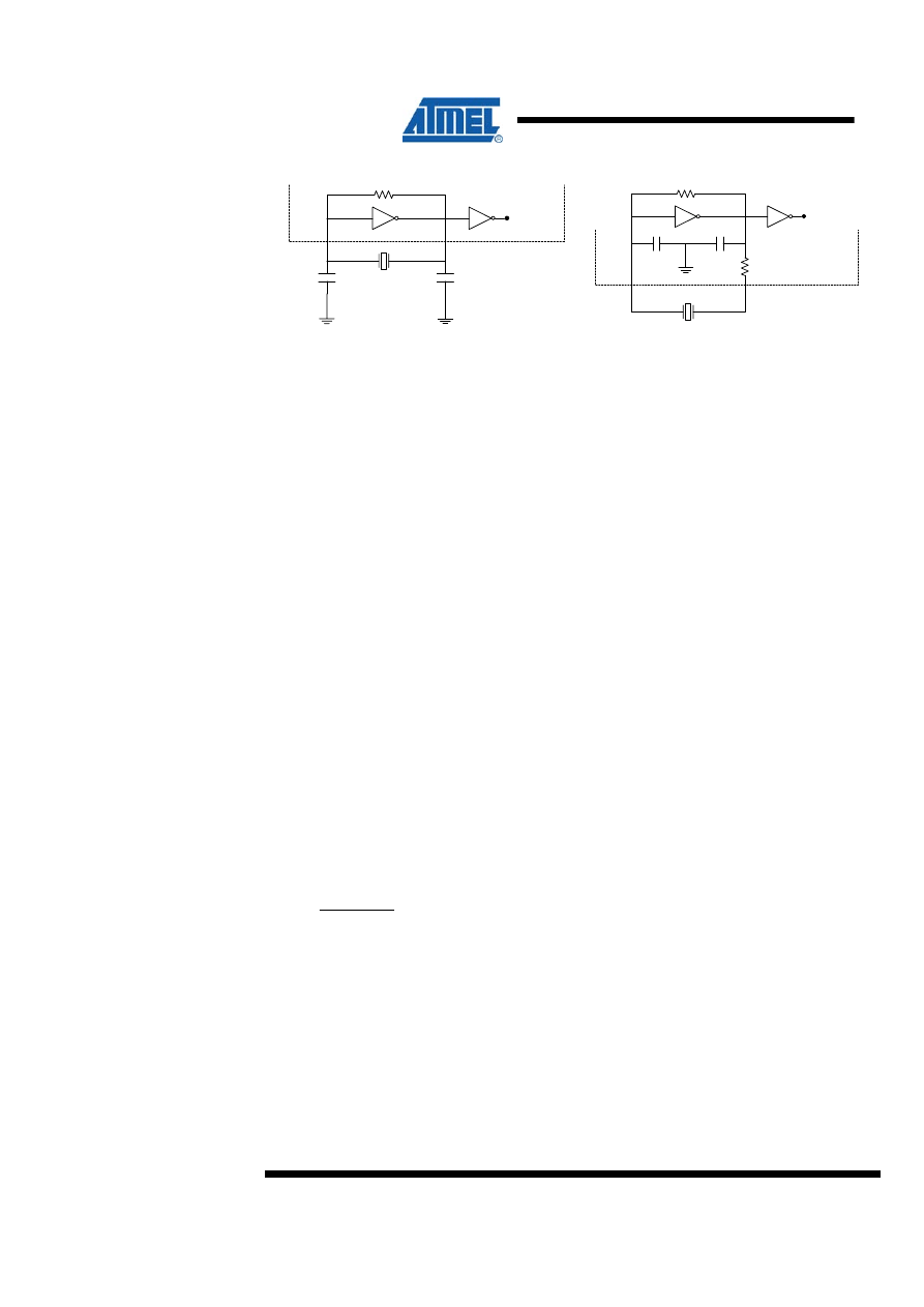
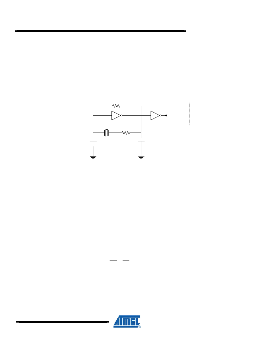
for parallel resonators are illustrated in Figure 5-1. The part of the circuit above the
dashed line, represent the oscillator circuit internally in the AVR.
8
AVR042
Figure 5-1. Basic inverter circuits equivivalent to the oscillator circuits in AVRs.
Clock out
R
f
C
L2
C
L1
Xtal
XTAL1
XTAL2
(A)
Clock out
R
f
C
L2
C
L1
Xtal
XTAL1/
TOSC1
XTAL2/
TOSC2
R
b
(B)
Notes:
i.
Oscillator circuit for crystals and ceramic resonators faster than 400kHz
ii.
Circuit for low frequency crystals (32.768kHz) (not on all AVRs)
Simplifying the description of the AVRs built-in oscillator circuits they can be
understood as the inverter based oscillator circuits illustrated in Figure 5-1. The circuit
used with resonators of frequencies above 400kHz is depicted in (A). When using this
circuit, capacitive load must be applied externally. The oscillator circuit seen in (B) is
the circuit used for low frequency crystals on some AVRs - to be more specific -
optimized for 32.768kHz crystals. This circuit provides the capacitive load required by
the crystal internally and further adds the resistor R
b
to bias the crystal and limit the
drive current into the crystal. The resistor R
f
is, when using CMOS inverters,
approximately 1Mohm, and provides a feedback to bias the inverter to operate it in its
linear region. Consult data sheet for the relevant device to see if is has internal
circuitry for low frequency crystals.
When using resonators with the AVR, it is necessary to apply (external) capacitors
according to the requirements of the facilitated resonator. A parallel resonator will not
be able to oscillate stable if the capacitive load applied is insufficient. If the capacitive
load is too high the oscillation may have problems starting due to drive level
dependency of the load. The trick is therefore to find an appropriate value for the
capacitive load. The value to look for in the data sheet of the crystal is C
L
, the
recommended capacitive load of the resonator (viewed from the terminals of the
resonator). The capacitive load, C
L,
of the oscillator circuit, including stray
capacitances and the capacitances of the XTAL pins of the AVR can be determined
empirically or it can be estimated by Equation 5-1.
Equation 5-1.
'
2
'
1
'
2
'
1
L
L
L
L
L
C
C
C
C
C
+
⋅
=
,
S
L
L
L
S
L
L
L
C
C
C
C
C
C
2
2
'
2
1
1
'
1
+
=
+
=
Where C
L1
and C
L2
refer to the external capacitors seen in Figure 5-1 and C
L1S
and
C
L2S
are stray capacitances at the XTAL pins of the AVR. Assuming symmetric layout,
so that C
L1
= C
L2
= C and C
L1S
= C
L2S
= C
S
, then the external capacitors can be
determined by Equation 5-2 (C
S
can be estimated to be 5-10pF):
Equation 5-2.
S
L
C
C
C
−
⋅
= 2
2521F-AVR-04/08
AVR042
5.3 Safety factor
To avoid overloading the crystal, so that it does not start up, the safety factor of the
oscillator (including the specific crystal) should be verified. Overload does in general
not cause start-up problems for ceramic resonators and therefore this section
primarily applies to the use of crystals. To verify the safety factor of the oscillator, the
resonance load (or oscillation allowance) must be determined. By inserting a resistor
(R
Q
) in series with the crystal (temporarily), as illustrated in Figure 5-2, the resonance
load is determined. Oscillation allowance, or OA, is defined in Equation 5-3.
Figure 5-2. R
Q
in series with the crystal to determine the resonance load.
Clock out
R
f
C
L2
C
L1
Xtal
XTAL1
XTAL2
R
Q
The way to do the test is to vary the external capacitors from a low capacitive load to
a load where the oscillator stops oscillating. Make sure to mount the capacitors firmly,
- avoid any kind of sockets.
Start the AVR having C
L1
and C
L2
as low as 1-2pF and verify that the oscillator is
actually oscillating. If a current probe is available this can be used to investigate if the
crystal is oscillating, otherwise a small test program toggling a pin on one of the I/O
ports can be used to accomplish this. Increase C
L1
and C
L1
until the oscillator stops
oscillating. Determine the safety factor by Equation 5-4. It is recommended to use a
capacitive load that results in a Safety Factor of 3-5.
Equation 5-3.
L
Q
R
R
Allowance
n
Oscillatio
+
=
Equation 5-4.
1
+
=
=
L
Q
L
R
R
R
OA
Factor
Safety
Where the resonance load R
L
is determined by Equation 5-5:
Equation 5-5.
2
0
1
1
⎟⎟
⎠
⎞
⎜⎜
⎝
⎛
+
⋅
=
L
L
C
C
R
R
9
2521F-AVR-04/08
10
AVR042
Where R
1
and C
0
are obtained from the datasheet of the resonator and C
L
is the
applied capacitive load calculated using Equation 5-1.
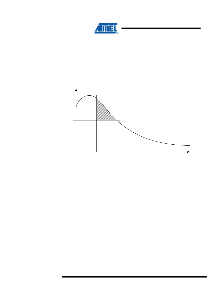
In the optimal test the curvature of the safety factor as a function of the applied
capacitive load should be determined. If this is done one should be aware that it is not
recommended to be at the top-point of the safety factor curvature, but rather at a
point where the curve has started falling. Result of the test could look like the one
seen in Figure 5-3.
Figure 5-3. Safety factor curvature for a given value of R
Q
C
L1
/ C
L2
[pF]
Safety factor
4
5
3
2
1
5
10
15
20
25
35
45
55
30
40
50
60
70
65
RQ=xx Ohm
In the example in Figure 5-3 the hatched area indicates the safe area. In general the
safety factor should be above 3 for the oscillator to be considered in the safe region of
operation. Other factors should though be considered as well: The minimum required
capacitive load, the recommended and the maximal drive level.
5.4 Recommended capacitor values
The recommendations here will work well in most applications, but there is no way to
provide general values for the external capacitors that can be guarantee to work with
all resonators.
When using the clock option “ext. crystal oscillator”, crystals with a nominal frequency
from 400 kHz and up can be used. For these standard “high” frequency crystals the
recommended capacitor value is in the range 22-33pF.
The clock option “ext. low frequency crystal” is intended for 32.768kHz crystals. When
selecting this clock source the internal oscillator circuit might provide the required
capacitive load. By programming the CKOPT Fuse, the user can enable internal
capacitors on XTAL1 and XTAL2. The value of the internal capacitors is typical 20pF,
but can vary. If using a 32.768kHz crystal that does not require more load than this,
external capacitors can be left out. Otherwise external capacitive load must be added.
In this case the capacitive load value, given by the manufacturer of the crystal, should
2521F-AVR-04/08

AVR042
11
2521F-AVR-04/08
be used. Then the value of the external capacitors can be determined by Equation 2.
The CKOPT Fuse should be unprogrammed when using external capacitors.
Please reefer to the datasheet to assure whether the device has internal capacitors or
not. Devices who support 1.8-5.5V operating voltages do not have internal capacitors
(except Atmega162). Note that AT90S8535, Atmega163 and Atmega103 does not
have the CKOPT-fuse, instead they have dedicated pins (TOSC1-TOSC2), to
connect the 32.768 kHz watch crystal to.
Using the clock option that selects “ext. ceramic resonator” it is strongly
recommended to consult the datasheet to determine the capacitors to apply. Always
use the capacitive load recommended there since the resonant frequency of the
ceramic resonators is very sensitive to capacitive load.
5.5 Pullability of the nominal frequency
The frequency of the resonator is depending on the capacitive load that is applied.
Applying the capacitive load specified in the datasheet of the resonator will provide a
frequency very close to the nominal frequency (intended oscillating frequency). If
other capacitive loads are applied the oscillating frequency will change. The
frequency will increase if the capacitive load is decreased and decrease if the load is
increased. The frequency pullability - how far from the nominal frequency the
resonant frequency can be forced by applying load - is depending on the type of
resonator used or actually the Q-factor of the resonator. Typically crystals have a very
high Q-factor, meaning that the pullability of the resonant frequency is relatively low.
Some crystals have especially high Q-factors, e.g. 32.768kHz crystals since they are
typically used for timing purposes, which require that the frequency is very exact.
Ceramic resonators do not have high Q-factors and are therefore more sensitive to
changes in capacitive load.
Regardless of the resonator type the resonant frequency can be pulled, by changing
the capacitive load, but if a high capacitive load is applied it must be ensured that the
oscillator can start in all conditions of operation. If the resonator is overloaded the
oscillation can have problems starting, but once the oscillation has started it will
seldom stop again due to overload. Touching the pins of a resonator that have not
started oscillating, with a finger or an oscilloscope-probe, can be sufficient to start the
oscillation and it can therefore be tricky to identify the overload problem.
To be able to determine the pullability of the resonator the “motional” capacitance of
the resonator should be know. This value is not listed in all crystal datasheet and it is
recommended to not intentionally try to pull the resonant frequency of the resonator
unless understanding the theory behind this
5.6 Unbalanced external capacitors
In noisy environments the oscillator can be affected crucially by the noise. If the noise
is strong enough the oscillator can “lock up” and stop oscillating. To make the
oscillator less sensitive to noise the size of the capacitor at the high impedance input
of the oscillator circuit, XTAL1, can be increased slightly. Increasing only one of the
capacitors does not affect the total capacitive load much, but unbalanced capacitors
can affect the resonant frequency to a higher degree than the change of the total
capacitive load. However, unbalanced capacitive loads will affect the duty cycle of the
oscillation and therefore one should in general not use unbalanced capacitive loads.
This is especially critical if running the AVR close to it’s maximum speed limit.

12
AVR042
2521F-AVR-04/08
5.7 RTC crystals
Many AVR devices have the possibility use asynchronous clocking of the built-in
timer/counter. The counter can through this feature be used for real time functions. A
32.768KHz crystal should then be connected to the TOSCx pins of the AVR.
In some AVRs the internal oscillator circuit used with the real time counter provides a
capacitive load of approximately 20pF, which should be appropriate for common
32.768KHz crystals. Refer to the data sheet for the relevant device for info about
capacitors/size. External capacitors can be applied if the internal load is insufficient
for the applied crystal.
5.8 PCB layout
Finally, the importance of the physical location of the resonator in relation to the AVR
should be stressed. Always place the resonator as close to the AVR as possible and
shield the resonator by surrounding it with a ground plane.
6 Example layout
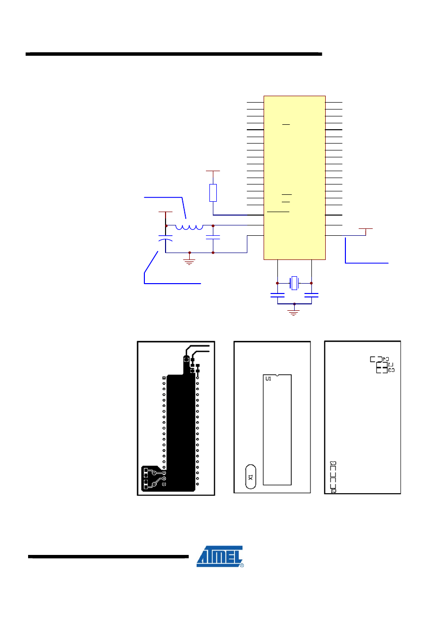
Figure 6-1 (A-D) shows a schematic and PCB layout using a crystal oscillator for
ATmega8515, decoupling digital supply from VCC is seen. Note the ground plane
surrounding the crystal and the very short distance between the crystal and the
ATmega8515.
AVR042
Figure 6-1. (A) basic schematic of required/recommended connections for
AT90S8515. (B) Copper PCB layout. (C) and (D) top and bottom silk prints.
X1
7M372
C1
22p
C2
22p
PB0/T0
1
PB1/T1
2
PB2/AIN0
3
PB3/AIN1
4
PB4/SS
5
PB5/MOSI
6
PB6/MISO
7
PB7/SCK
8
PD0/RXD
10
PD1/TXD
11
PD2/INT0
12
PD3/INT1
13
PD4
14
PD5/OC1A
15
PD6/WR
16
PD7/RD
17
AD7/PA
32
AD6/PA
33
AD5/PA
34
AD4/PA
35
AD3/PA
36
AD2/PA
37
AD1/PA
38
AD0/PA
39
A8/PC0
21
A9/PC1
22
A10/PC2
23
A11/PC3
24
A12/PC4
25
A13/PC5
26
A14/PC6
27
A15/PC7
28
RESET
9
XTAL1
19
XTAL2
18
ALE
30
OC1B
29
ICP
31
VCC
40
GND
20
U1
ATmega8515
C3
100n
L1
47n
VCC
VCC
VCC
13
2521F-AVR-04/08
R1
4.7k
Connect ICP to
Vcc if not used
Inductor improves
ower filtering
p
C4
4.7uF/6
Tantal capacitor
(A)
(B)
(C)
(D)

Disclaimer
Headquarters
International
Atmel Corporation
2325 Orchard Parkway
San Jose, CA 95131
USA
Tel: 1(408) 441-0311
Fax: 1(408) 487-2600
Atmel Asia
Room 1219
Chinachem Golden Plaza
77 Mody Road Tsimshatsui
East Kowloon
Hong Kong
Tel: (852) 2721-9778
Fax: (852) 2722-1369
Product Contact
Atmel Europe
Le Krebs
8, Rue Jean-Pierre Timbaud
BP 309
78054 Saint-Quentin-en-
Yvelines Cedex
France
Tel: (33) 1-30-60-70-00
Fax: (33) 1-30-60-71-11
Atmel Japan
9F, Tonetsu Shinkawa Bldg.
1-24-8 Shinkawa
Chuo-ku, Tokyo 104-0033
Japan
Tel: (81) 3-3523-3551
Fax: (81) 3-3523-7581
Web Site
www.atmel.com
Technical Support
avr@atmel.com
Sales Contact
www.atmel.com/contacts
Literature Request
www.atmel.com/literature
Disclaimer: The information in this document is provided in connection with Atmel products. No license, express or implied, by estoppel or otherwise, to any
intellectual property right is granted by this document or in connection with the sale of Atmel products. EXCEPT AS SET FORTH IN ATMEL’S TERMS AND
CONDITIONS OF SALE LOCATED ON ATMEL’S WEB SITE, ATMEL ASSUMES NO LIABILITY WHATSOEVER AND DISCLAIMS ANY EXPRESS, IMPLIED
OR STATUTORY WARRANTY RELATING TO ITS PRODUCTS INCLUDING, BUT NOT LIMITED TO, THE IMPLIED WARRANTY OF MERCHANTABILITY,
FITNESS FOR A PARTICULAR PURPOSE, OR NON-INFRINGEMENT. IN NO EVENT SHALL ATMEL BE LIABLE FOR ANY DIRECT, INDIRECT,
CONSEQUENTIAL, PUNITIVE, SPECIAL OR INCIDENTAL DAMAGES (INCLUDING, WITHOUT LIMITATION, DAMAGES FOR LOSS OF PROFITS,
BUSINESS INTERRUPTION, OR LOSS OF INFORMATION) ARISING OUT OF THE USE OR INABILITY TO USE THIS DOCUMENT, EVEN IF ATMEL HAS
BEEN ADVISED OF THE POSSIBILITY OF SUCH DAMAGES. Atmel makes no representations or warranties with respect to the accuracy or completeness of the
contents of this document and reserves the right to make changes to specifications and product descriptions at any time without notice. Atmel does not make any
commitment to update the information contained herein. Unless specifically provided otherwise, Atmel products are not suitable for, and shall not be used in,
automotive applications. Atmel’s products are not intended, authorized, or warranted for use as components in applications intended to support or sustain life.
© 2008 Atmel Corporation. All rights reserved. Atmel®, logo and combinations thereof AVR®, and others, are the registered trademarks or
trademarks of Atmel Corporation or its subsidiaries. Other terms and product names may be trademarks of others.
2521F-AVR-04/08
Document Outline
- 1 Introduction
- 2 Power Supply
- 3 Connection of RESET pin on AVRs
- 4 Connecting ISP lines
- 5 Using crystal and ceramic resonators
- 6 Example layout
Wyszukiwarka
Podobne podstrony:
AVR Hardware Design Considerations
doc2521 AVR Hardware Design Considerations
Design Guide 03 Serviceability Design Considerations for Low Rise Buildings
Eurocode 6 Part 2 1996 2006 Design of Masonry Structures Design Considerations, Selection of Mat
Eurocode 6 Part 2 1996 2006 Design of Masonry Structures Design Considerations, Selection of Mat
PICmicro Application Design and Hardware Interfacing
avr spis tresci
AVR na Linuxie
Bootloader dla mikrokontrolerów AVR
evboard, Płytka testowa dla mikrokontrolerów AT89S oraz AVR
History Costume History Costume Design Viking Women
Eurocode 5 EN 1995 1 1 Design Of Timber Structures Part 1 1 General Rules
elebot avr
CAN on the AVR
[Instrukcja] GDOT Design Policy Manual Chapter 8 Roundabouts (USA)
FX3U Hardware A4 pol
więcej podobnych podstron