A New Medium Voltage PWM Inverter Topology for Adjustable Speed Drives
E. Cengelci*, S. U. Sulistijo*, B. O. Woo*, P. Enjeti*,
R. Teodorescu**, F. Blaabjerg**
Power Quality Laboratory*
Department of Electrical Engineering
Texas A&M University
College Station, TX – 77843
Tel: 409-845-7466
Fax: 409-845-6259
Email: enjeti@tamu.edu
Institute of Energy Technology**
Department of Electrical Engineering
Aalborg University
9220 Aalborg East, Denmark
Tel: 45 96 35 92 54
Fax: 45 98 15 14 11
Email: fbl@iet.auc.dk
Abstract: In this paper a new PWM inverter topology suitable for
medium voltage (2300 / 4160 V) adjustable speed drive (ASD)
systems is proposed. The modular inverter topology is derived by
combining three standard 3-phase inverter modules and a 0.33
pu output transformer. The output voltage is high quality, multi-
step PWM with low dv/dt. Further, the approach also guarantees
balanced operation and 100% utilization of each 3-phase inverter
module over the entire speed range. These features enable the
proposed topology to be suitable for powering constant torque as
well as variable torque type loads. Clean power utility interface of
the proposed inverter system can be achieved via an 18-pulse
input transformer. Analysis, simulation, and experimental results
are shown to validate the concepts.
1. INTRODUCTION
Power converters for medium voltage adjustable speed drive
(ASD) systems (2300V, 4160V) are primarily current
source inverter (CSI) based [5]. The CSI approach employs
SCR/GTO devices and has the following disadvantages:
higher cost per kW; suffers from stability problems;
unsuitable for running multiple motors from a single
inverter; can excite torsional resonance’s in the motor;
results in increased motor heating and poor input current
quality. On the other hand, the conventional voltage source
inverter (VSI) for medium voltage ASDs suffers from high
output dv/dt; elevated common mode output voltage & dv/dt
which necessitates additional motor insulation or a
dedicated output isolation transformer in retrofit
applications.
Both of the above CSI/VSI approaches employ power
devices which are manufactured in low volume. With
corrective measures to improve utility power quality, the
cost of the overall medium voltage ASD per kW is at least
five times the cost per kW of a present day 480V PWM
ASD employing IGBT devices. In view of this, references
[1-4] have suggested the use of series connected single-
phase PWM inverter modules for medium voltage ASD
systems. This topology despite its many advantages suffers
from the following drawbacks:
i.
Employs many series connected single-phase
inverter modules.
M
K
L
M
c
1
a
1
b
1
3 P h a s e
Inverter
M o d u l e
1
c
3
a
3
b
3
3 P h a s e
Inverter
M o d u l e
3
c
2
a
2
b
2
3 P h a s e
Inverter
M o d u l e
2
1
2
3
V
D C
+
-
V
D C
+
-
V
D C
+
-
(a)
L
a
2
2
b
2
K
b
1
c
1
1
a
1
b
3
M
3
c
3
a
3
c
2
(b)
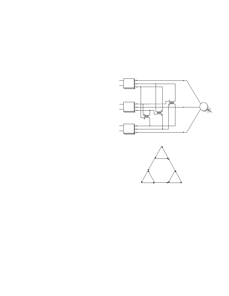
Fig. 1. (a) Proposed new medium voltage PWM inverter topology.
(V
dc
= 1090V, IGBT’s rated at 1700V for 2300V ac (rms) output)
(V
dc
= 1970V, IGBT’s/IGCT’s rated at 3300V for 4160V ac (rms) output)
(b) Vector diagram of the system with the fundamental voltages.
ii.
In constant torque applications at low speeds, the
dc-link capacitive energy storage requirements are
high.
iii.
Larger number of single-phase inverter modules
also require larger number of isolated secondary
windings in the input transformer which results in
higher manufacturing cost.
In this paper a new medium voltage PWM inverter topology
is proposed [6]. The proposed inverter employs three
standard 3-phase PWM inverter modules along with a 0.33
pu output transformer (Figs. 1 and 2). The advantages of the
proposed system can be summarized as follows:
0-7803-4943-1/98/$10.00 (c) 1998 IEEE
M
i
a
2
V
dc
+
-
V
dc
+
-
V
dc
+
-
-20
o
3-phase
Rectifier/Inverter
ASD modules
Output
transformer
Medium
voltage ASD
a
1
b
1
c
1
a
2
b
2
c
2
a
3
b
3
c
3
s
t
v
r
q
p
o
w
x
y
z
u
i
1
i
2
i
3
i
4
i
5
i
6
K
L
M
0
o
+20
o
A
C
B
3-Phase
medium voltage
utility
18-pulse
polyphase
transformer
I
A
I
B
I
C
A
1
B
1
C
1
A
2
B
2
C
2
A
3
B
3
C
3
1
2
3
i
c
1
i
b
1
i
a
1
i
c
2
i
b
2
i
a
3
i
b
3
i
c
3
i
o
1
i
o
2
i
o
3
(a)
K
M
a
3
b
3
3
c
3
a
1
1
b
1
c
1
c
2
2
a
2
b
2
L
o
p
s
t
x
w
q
r
z
y
u
v
i
1
i
2
i
4
i
5
i
6
i
3
i
a
1
i
c
1
i
b
1
i
a
3
i
c
3
i
b
3
i
a
2
i
c
2
i
b
2
o
p
q
r
s
t
u
v
w
x
y
z
i
1
i
2
i
3
i
4
i
5
i
6
(b) (c)
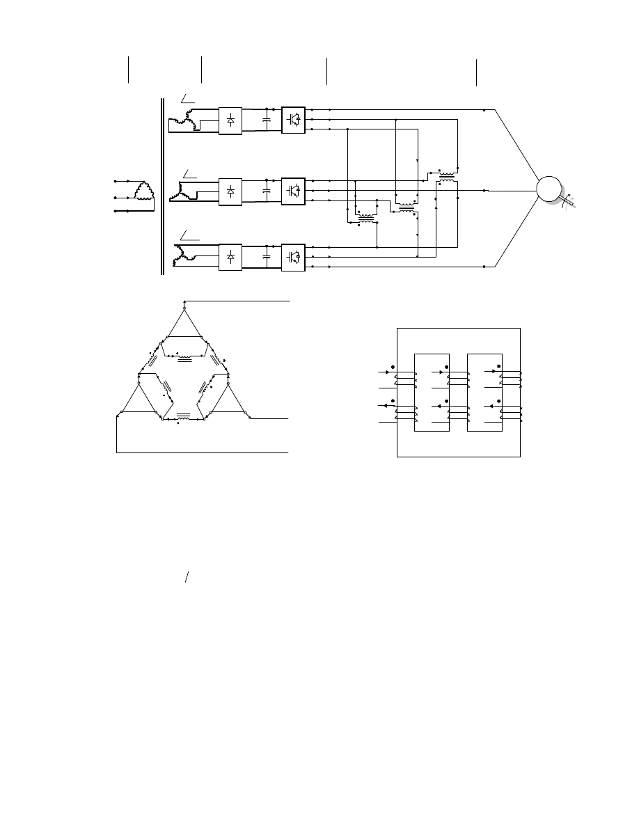
Fig. 2 (a) Complete medium voltage ASD with the proposed topology along with an 18-pulse input transformer for clean input power. (b) Connection of
inverter modules and the output transformer. (c) Winding configuration of output transformer on a three- limb core.
i.
Only three standard 3-phase rectifier/inverter
modules are necessary to generate medium voltage
output.
ii.
Each inverter is balanced in operation, equally
loaded and supplies 3
1
output power.
iii.
Modular construction of the medium voltage
inverter system facilitates the use of lower voltage
IGBT devices which are available in larger volume,
easy maintenance and spare management.
iv.
The output voltage is 3 pu, high quality multilevel
PWM with low dv/dt.
v.
The dc-link capacitive energy storage requirement is
low due to balanced operation of each three-phase
inverter module.
vi.
The proposed system is suitable for powering
constant/variable torque type loads over a wide
speed range.
vii.
The inverter system is flexible for generating
different medium voltage levels for ASD
applications.
viii.
The output transformer contributes to higher output
voltage and eliminates any circulating current
within the inverter modules.
2. OPERATION OF THE INVERTER SYSTEM
Fig.1a shows the interconnection of three standard 3-phase
inverter modules along with an output transformer to
generate higher output voltage. The vector diagram
representing the complete inverter system is shown in Fig.
1b. Each three-phase inverter generating balanced three-
phase output voltages is represented by a delta. For
example,
1
a ,
1
b and
1
c (Fig. 1b) represent the inverter
module-1 in Fig. 1a. Also three transformers of 1:1 turn
ratio are connected to the inverter output (Fig. 1a). The
purpose of the output transformer is to generate the vectors
(Fig. 1a, 1b)
3
1
a
c
,
2
3
c
b
,
1
2
b
a
from inverter output voltage
vectors
2
2
c
a
,
1
1
b
c
and
3
3
a
b
, respectively. A more detailed
connection diagram of the output transformer to accomplish
this task is shown in Fig. 2. The output transformer
0-7803-4943-1/98/$10.00 (c) 1998 IEEE

therefore increases the output voltage and also ensures that
the addition of voltage vectors (Fig. 1b)
1
1
b
c
,
2
1
a
b
,
2
2
c
a
,
3
2
b
c
,
3
3
a
b
and
1
3
c
a
is zero at any switching instant, this
eliminates any circulating current within the loop.
The proposed inverter topology can power a 2300V
adjustable speed drive system with a dc bus voltage
=
dc
V
1090V. Hence IGBT’s rated at 1700V or higher can
be employed. Further, a
=
dc
V
1970V is sufficient to power
a 4160V adjustable speed drive system. For 4160V output
each inverter IGBT’s/IGCT’s could be rated at 3300V.
Further details are available in section 4.
Fig. 2a shows an approach to interface the proposed inverter
topology to electric utility via an 18-pulse transformer. The
input transformer essentially has three secondary windings
arranged in 0
°
,
±
20
°
phase shift to achieve harmonic current
cancellation in the utility line currents. Since each three-
phase inverter is loaded equally, the 5
th
, 7
th
, 11
th
, and 13
th
,
harmonic currents generated by each rectifier/inverter
module are cancelled in the input line. This results in clean
input power.
3. ANALYSIS
In this section analysis of the modular inverter system is
presented. Considering Fig. 2a, the load (motor) is
connected to inverter terminals
1
a ,
2
b and
3
c . Assuming a
balanced load, the fundamental components of the load
currents can be expressed as
)
sin(
2
1
t
I
i
a
ω
=
)
120
sin(
2
2
°
−
=
t
I
i
b
ω
(1)
)
120
sin(
2
3
°
+
=
t
I
i
c
ω
From Fig. 2b, the following equations can be written:
6
4
1
i
i
i
a
−
=
(2)
2
6
2
i
i
i
b
−
=
(3)
Since the voltage vectors
1
1
b
c
,
2
1
a
b
,
2
2
c
a
,
3
2
b
c
,
3
3
a
b
and
1
3
c
a
within the hexagon formed by the windings of the
output transformer, shown in Fig. 2b, add to zero at any
instant of time, there is no circulating current in the loop.
Therefore,
0
6
4
2
=
+
+
i
i
i
(4)
From (1) to (4) the currents
2
i ,
4
i ,
6
i can be solved as,
)
90
sin(
3
2
2
°
+
=
t
I
i
ω
)
30
sin(
3
2
4
°
−
=
t
I
i
ω
(5)
)
150
sin(
3
2
6
°
−
=
t
I
i
ω
Assuming that the output transformer has a large
magnetizing impedance, we have
2
1
i
i
=
4
3
i
i
=
(6)
6
5
i
i
=
The output currents of each inverter can be written as (Fig.
2b):
1
6
1
i
i
i
b
−
=
4
1
1
i
i
i
c
−
=
6
3
2
i
i
i
a
−
=
3
2
2
i
i
i
c
−
=
(7)
5
4
3
i
i
i
a
−
=
2
5
3
i
i
i
b
−
=
Using (1), (5), (6) and (7), the output currents of each
inverter module can be shown to be,
)
sin(
2
3
2
1
t
I
i
i
i
a
a
a
ω
=
=
=
)
120
sin(
2
3
2
1
°
−
=
=
=
t
I
i
i
i
b
b
b
ω
(8)
)
120
sin(
2
3
2
1
°
+
=
=
=
t
I
i
i
i
c
c
c
ω
The fundamental component (rms) of the output voltage of
inverter-1 (Fig. 2) is given by [5],
a
dc
b
a
m
V
V
2
2
3
1
1
=
(9)
where
dc
V is the dc-link voltage and
a
m is the amplitude
modulation index [5]. The range for
a
m for a sinusoidal
(with third harmonic injection) or space vector modulation
is
15
.
1
0
≤
≤
a
m
Similarly, the fundamental output voltages of inverter-2 and
inverter-3 are given by,
a
dc
b
a
m
V
V
2
2
3
2
2
=
(10)
0-7803-4943-1/98/$10.00 (c) 1998 IEEE
and
a
dc
b
a
m
V
V
2
2
3
3
3
=
(11)
Now due to transformer action,
2
1
3
3
a
b
b
a
V
V
=
(12)
Therefore, the fundamental line-to-line output voltage of the
medium voltage inverter system is given by (Fig. 1b),
2
2
2
1
1
1
b
a
a
b
b
a
KL
V
V
V
V
+
+
=
(13)
From (9) to (13), we have,
a
dc
KL
m
V
V
2
2
3
3
=
(14)
Also, fundamental output VA of each inverter module is
given by,
rms
a
b
a
I
V
VA
,
1
1
1
1
3
⋅
⋅
=
rms
a
b
a
I
V
VA
,
2
2
2
2
3
⋅
⋅
=
(15)
rms
a
b
a
I
V
VA
,
3
3
3
3
3
⋅
⋅
=
From (8), (9), (10), (11) and (15), it can be shown that
I
m
V
VA
VA
VA
a
dc
2
2
3
3
2
1
=
=
=
(16)
Thus, (16) demonstrates that each inverter module is equally
loaded and fully utilized. Further, the total output VA of the
medium voltage inverter system is given by,
rms
a
KL
total
I
V
VA
,
1
3
⋅
⋅
=
I
m
V
a
dc
2
2
9
=
(17)
Comparing (16) to (17) it is clear that
total
VA
is three times
the VA rating of each inverter.
Equations (8) and (16) suggest that output currents of each
3-phase inverter are balanced and each inverter is fully
utilized. It should be noted that balanced operation of each
inverter module does not generate any low frequency
current components in the inverter input currents (
1
o
i ,
2
o
i ,
3
o
i ) when the output frequency is widely varied, particularly
at reduced speed. This is an important advantage of the
proposed inverter topology compared to the approach
discussed in [1-4].
3.A. VA Rating Of The Output Transformer:
Fig. 2 shows the connection diagram of the output
transformer. (5) and (6) illustrate the transformer winding
currents. Further, from (9) to (12) voltages across the
transformer windings are given by,
a
dc
rms
qr
rms
op
m
V
V
V
2
2
3
,
,
=
=
a
dc
rms
yz
rms
wx
m
V
V
V
2
2
3
,
,
=
=
(18)
a
dc
rms
uv
rms
st
m
V
V
V
2
2
3
,
,
=
=
Using (5) and (6), the rms currents through the output
transformer windings are
3
6
5
4
3
2
1
I
I
I
I
I
I
I
=
=
=
=
=
=
(19)
The VA rating of the output transformer can be computed as
follows:
+
⋅
+
⋅
+
⋅
=
3
,
6
,
1
,
(
2
1
I
V
I
V
I
V
VA
rms
st
rms
yz
rms
op
tr
)
4
,
5
,
2
,
I
V
I
V
I
V
rms
uv
rms
wx
rms
qr
⋅
+
⋅
+
⋅
(20)
Using (18), (19) and (20),
I
m
V
VA
a
dc
tr
2
2
3
=
(21)
Comparing (17) to (21), it is clear that VA rating of the
output transformer is
3
1
of total VA rating of the inverter
output.
4. DESIGN EXAMPLE
In this section a detailed design example of a 2300V,
2000hp medium voltage inverter is discussed (Fig. 2).
Motor parameters:
Power
( )
HP
P
o
2000
=
Power factor
( )
8
.
0
=
pf
Efficiency
( )
85
.
0
=
η
Line-to-line voltage
( )
rms
KL
V
V
2300
=
Fundamental output frequency
Hz
f
o
60
=
Apparent power
( )
S and line current
(
)
rms
a
I
,
1
of the motor
can be calculated as follows:
0-7803-4943-1/98/$10.00 (c) 1998 IEEE
kVA
pf
P
S
o
2200
=
⋅
=
η
(22)
A
V
S
I
LL
rms
a
552
3
,
1
=
⋅
=
(23)
Since the rms inverter output currents are all equal and same
as the load currents, each 3-phase inverter module should be
rated for 552A.
By equating the output voltage
KL
V
in (14) to 2300V at
60Hz and assuming
1
.
1
=
a
m
5, we have
V
m
V
V
a
KL
dc
1090
3
3
2
2
=
⋅
⋅
=
(24)
Further, the rms current of the IGBT and diode pairs,
2
,
,
1
rms
a
rms
sw
I
I
=
. (25)
From (23) and (25)
A
I
rms
sw
390
,
=
(26)
Peak switch current is the same as peak motor current.
Therefore,
A
I
peak
sw
780
2
552
,
=
⋅
=
(27)
The IGBT’s in inverters are rated at rms current of 390A
and peak current of 780A. Further, IGBT’s rated at 1700V
or higher can be employed in each inverter module to
operate at a
=
dc
V
1090V.
If we assume the same motor parameters in the previous
design example, except the line-to-line voltage of the motor
( )
rms
KL
V
V
4160
=
, the inverter ratings are as follows:
From (24) to (27), we have,
V
V
dc
1970
=
,
A
I
rms
sw
215
,
=
,
A
I
peak
sw
431
,
=
The IGBT’s in inverters for 4160V motor design are rated at
rms current of 215A and peak current of 431A. IGBT’s
rated at 3300V [7] can be employed in each inverter module
to operate at a
=
dc
V
1970V.
5. PWM CONTROL STATEGY
In this section the necessary PWM control strategy required
to operate the proposed medium voltage topology (Fig. 1,
Fig. 2) is discussed. It is obvious that for proper operation of
( a )
t
Modulating signal
f o r p h a s e A
Triangular carier signal
for inverter-1
120
o
t
Modulating signal
f o r p h a s e A
Triangular carier signal
for inverter-2
(b)
240
o
t
Modulating signal
f o r p h a s e A
Triangular carier signal
for inverter-3
( c )
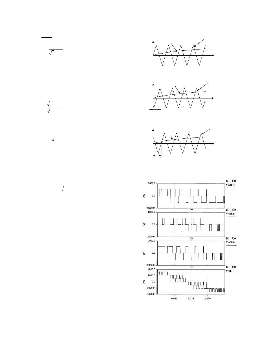
Fig. 3 PWM control strategy for the proposed topology (Notice the 120
°
phase-shift among the high frequency triangular carriers for inverters 1,2,3)
(d)
Fig.4 The voltages across “a” and “b” terminals of each 3-phase inverter
and the voltage across the motor terminals K and L.
0-7803-4943-1/98/$10.00 (c) 1998 IEEE
the modular inverter system the three 3-phase inverter
modules need to be synchronized. Further, the high
frequency triangular carriers employed in each inverter are
so chosen that a phase-shift of 120
°
exists between them.
Then the overall output voltage
KL
v
(Fig. 4) applied to the
motor is not only multi-step in nature but also low in
harmonic content.
Fig. 3 shows the intersection of high frequency triangular
carrier signals and the low frequency modulating sinusoidal
signal for one phase. Notice the 120
°
phase shift among the
high frequency triangular carriers employed for the control
of inverters 1, 2 and 3.
Fig. 4 (a), (b) and (c) show the line-to-line voltages of the
inverters 1, 2 and 3, i.e.
1
1
b
a
v
,
2
2
b
a
v
and
3
3
b
a
v
, respectively.
Fig. 4 (d) illustrates the overall output voltage
KL
v
, which is
multi-step in nature.
Assuming that the triangular carrier frequency is much
higher than the fundamental output frequency, the Fourier
components of voltages
1
1
b
a
v
,
2
2
b
a
v
and
3
3
b
a
v
can be
expressed as follows [5]:
( )
( )
∑
∞
=
+
=
2
sin
sin
1
1
h
h
dc
a
dc
b
a
t
h
A
V
t
m
V
v
ω
ω
( )
∑
∞
=
°
−
+
=
2
120
sin
sin
2
2
h
f
h
dc
a
dc
b
a
m
t
h
A
V
t
m
V
v
ω
ω
(28)
( )
∑
∞
=
°
+
+
=
2
120
sin
sin
3
3
h
f
h
dc
a
dc
b
a
m
t
h
A
V
t
m
V
v
ω
ω
where h is the order of the harmonics in the inverter output
voltage,
h
A is the amplitude of
th
h harmonic and
signal
modulating
of
Frequency
signal
carrier
triangular
of
Frequency
1
=
=
f
f
m
s
f
The phases of harmonics of
f
m
h
°
⋅
±
120
in the
expressions of
2
2
b
a
v
and
3
3
b
a
v
in (28) are primarily due to
the inherent 120
°
phase-shifts among the high frequency
triangular carrier signals (Fig. 3).
From Fig. 2 the overall inverter output voltage
KL
v
is,
3
3
2
2
1
1
b
a
b
a
b
a
KL
v
v
v
v
+
+
=
( )
+
=
t
m
V
a
dc
ω
sin
3
( )
t
h
m
h
A
V
h
f
h
dc
ω
sin
120
cos
2
1
2
∑
∞
=
°
⋅
+
(29)
For sine-triangular PWM, h is given by [5] as,
,
4
,
2
,
±
±
=
f
f
f
m
m
m
h
,
5
2
,
3
2
,
1
2
±
±
±
f
f
f
m
m
m
6
3
,
4
3
,
2
3
,
3
±
±
±
f
f
f
f
m
m
m
m
(30)
etc.
Substituting (30) into (29) we can deduce that for a large
value of
f
m (i.e. high switching frequency) the harmonic
components of h , around the side-bands of
f
m ,
f
m
2
,
f
m
4
,
f
m
5
, are cancelled in
KL
v
in (29). The dominant
harmonics in
KL
v
are around
f
m
3
. Therefore, in the
proposed PWM strategy the overall inverter line-to-line
output voltage (
KL
v
) is multi-step with the dominant
harmonics at three times the inverter switching frequency.
Also the voltage
KL
v
experiences level change in steps of
dc
V , which contributes to low
dt
dv
across the motor
terminals. Fig.5, Fig. 10, and Fig 11 validate the above
conclusions.
6. SIMULATION RESULTS
In this section simulation results of the proposed system
powering a 2300V motor detailed in the design example are
discussed. The switching frequency is set at 1kHz for each
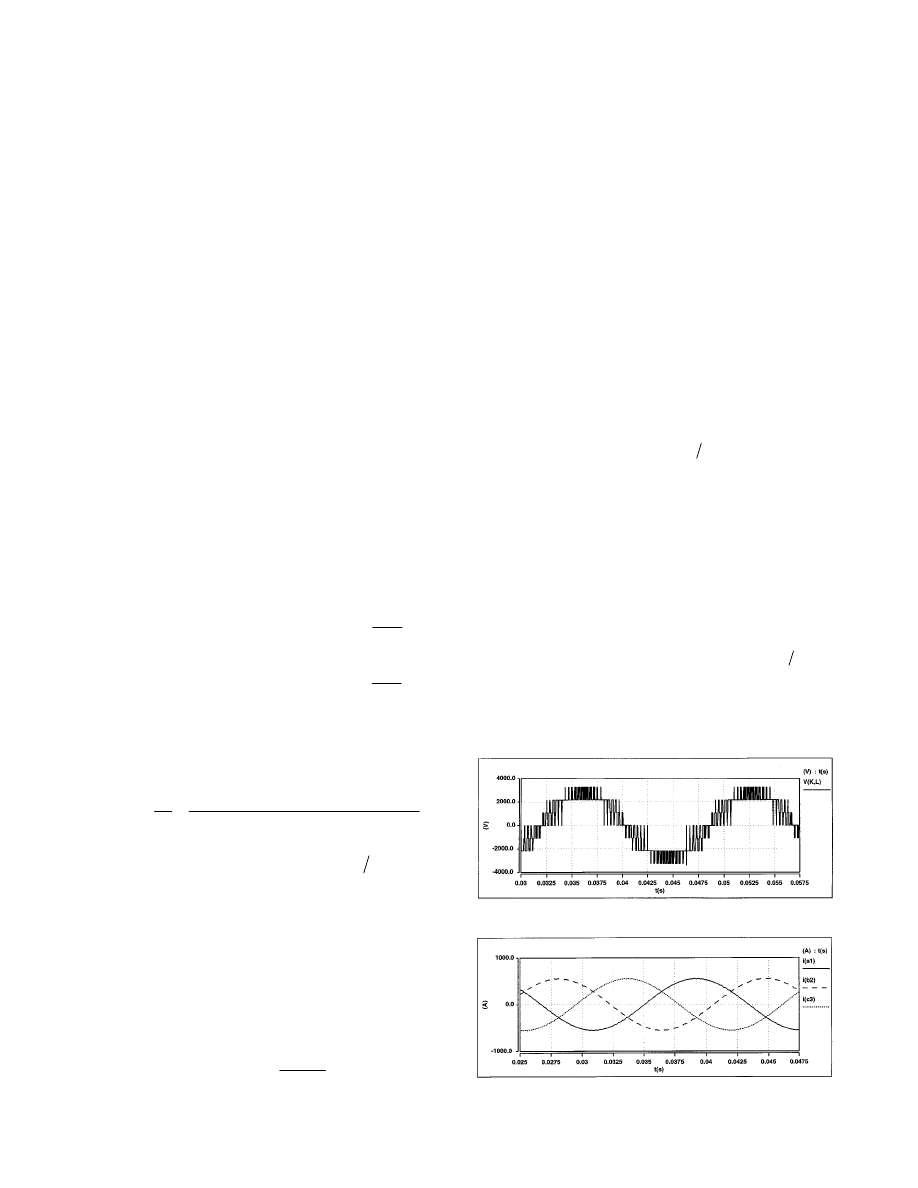
inverter module in the simulation. Fig. 5 shows the line to-
line output voltage of the inverter system across the motor
terminal. It is clear from Fig. 5 that the voltage across the
motor terminal is multilevel, therefore is of low
dt
dv
and
its harmonic content is also low. Fig. 6 shows the motor
currents, which are balanced and nearly sinusoidal. Lastly,
Fig. 7 shows the three output currents of an inverter module,
which are balanced.
Fig. 5 Line-to-line multi-step PWM voltage across the motor terminals.
Fig. 6 The currents of the motor (
1
a
i
,
2
b
i
,
3
c
i
).
0-7803-4943-1/98/$10.00 (c) 1998 IEEE
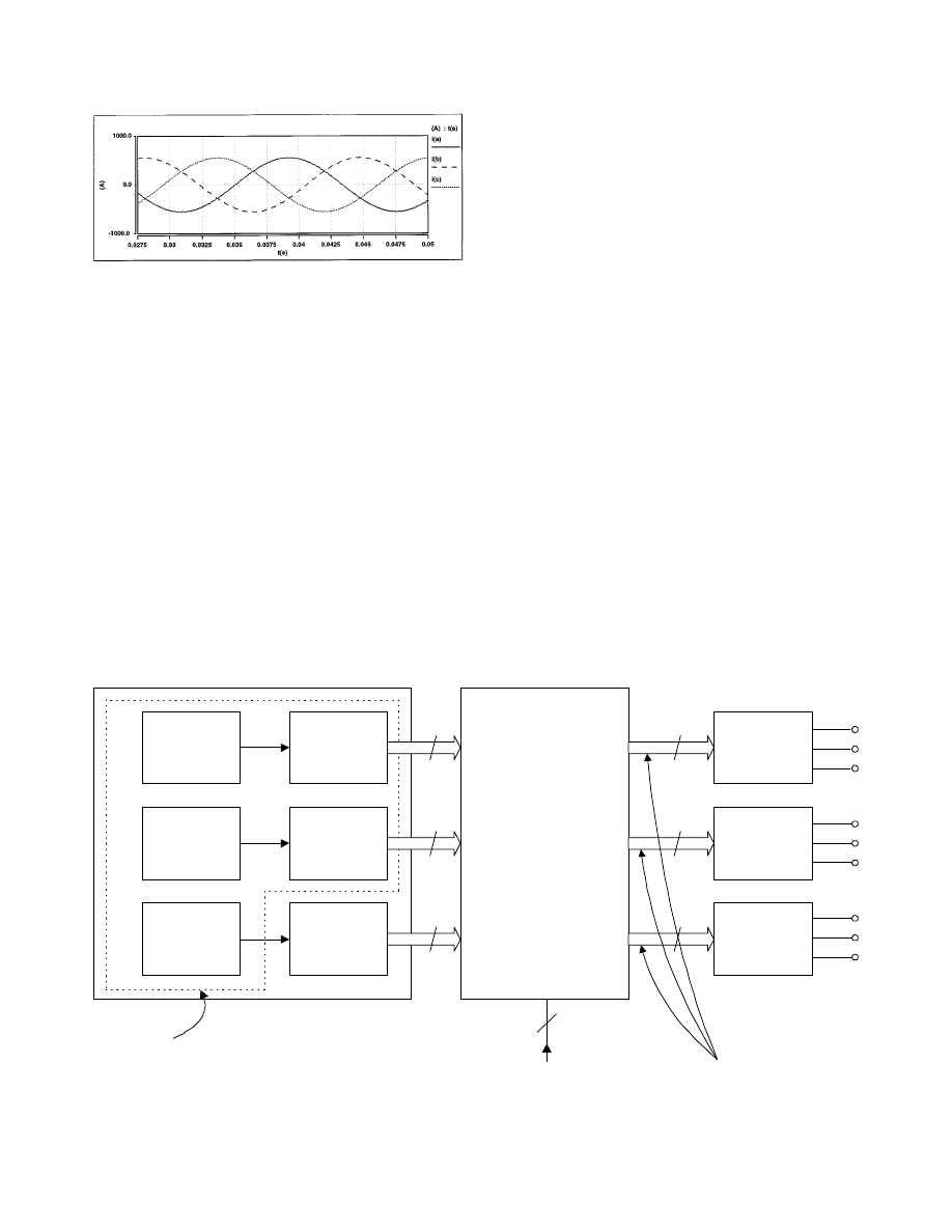
Fig. 7 O utput currents of inveter-1 (
1
a
i
,
1
b
i
,
1
c
i
).
7. EXPERIMENTAL RESULTS
A scale down experimental prototype of the proposed
inverter topology (Fig. 2) was tested in the laboratory for the
following specifications:
Dc bus voltages: 110V
Motor power: 4kW
Switching frequency: 1kHz
Fundamental output frequency: 50Hz
Fundamental voltage across the motor terminals: 260V
rms
The control signals for the inverter system in Fig. 2 are
obtained by using a DSP evaluation module of
TMS320F240 of Texas Instruments. TMS320F240 is a
fixed-point, 16 bit low cost DSP, incorporating a 20 MIPS
processor designed specifically for motor drive applications.
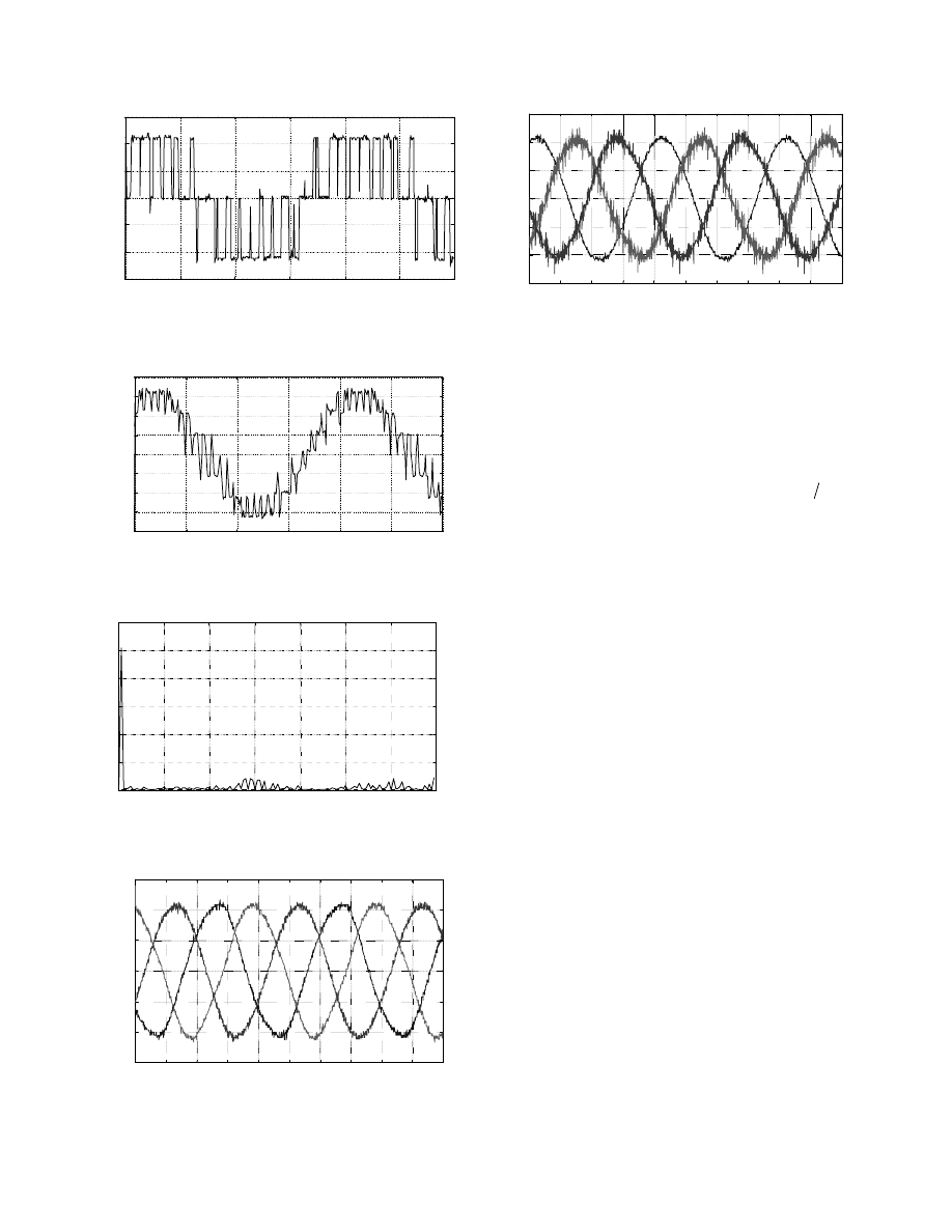
The block diagram of the PWM control system is shown in
Fig. 8. The PWM control signals for inverter-1 and -2 are
generated by the full compare and simple compare PWM
channels of the DSP (Fig. 8). The control signals for
inverter-3 are generated by software using GP Timer 3. The
full compare unit is capable of generating gating signals
with their dead-bands for inverter-1. However, the dead-
band generation of gating signals for inverters 2 and 3 is
obtained by hardware. The implementations of triangular
carrier signals are done by the GP timers 1, 2 and 3. A sine
table is used to implement the low frequency modulating
sinusoidal signals. The gating signals generated in the
control board are applied to the inverters via fiber optic
isolation hardware. A protection signal from each inverter is
fed back to the control hardware unit to ensure safe
operation of the system.
Fig. 9 shows the experimental PWM line-to-line voltage of
inverter-1. Fig. 10 shows the multilevel PWM voltage
KL
v
applied to the motor terminals. Fig. 11 shows the frequency
spectrum of voltage
KL
v
. The dominant harmonics in
KL
v
are around 3kHz, i.e. three times the inverter switching
frequency (Equation 29). Fig. 12 shows the motor currents
1
a
i ,
2
b
i ,
3
c
i (Fig. 2). Fig. 13 shows the inverter-1 output
currents
1
a
i ,
1
b
i ,
1
c
i . These results demonstrate the
feasibility of the proposed inverter topology. More
extensive tests are underway and will be reported at the
conference presentation.
GP Timer 1
GP Timer 2
GP Timer 3
Full Compare
6 PWM
Channels
with Dead-band
Simple
Compare
3 PWM
Channels
Output ports of
D/A Converter
Event Manager
TMS320F240 Evaluation Module
6
3
Optical Isolation
and Dead-band
Generation Module
3
3-Phase
Inverter 1
3-Phase
Inverter 2
3-Phase
Inverter 3
6
6
6
Fiber Optic Cables
a
1
b
1
c
1
a
2
b
2
c
2
a
3
b
3
c
3
Protection feedback signals
from three 3-phase inverters
3
Gating signals
for three
inverters
Fig. 8 DSP implementation of the PWM generation for the medium voltage inverter.
0-7803-4943-1/98/$10.00 (c) 1998 IEEE
0
0. 00 5
0. 01
0 .0 1 5
0 .0 2
0. 02 5
0 .0 3
-1 5 0
-1 0 0
-5 0
0
5 0
10 0
1 5 0
Fig. 9 Line-to-line output voltage of inverter-1 (
1
1
b
a
v
).
(Vertical scale: 50V/div, Horizontal scale:5ms/div)
0
0.005
0.01
0.015
0.02
0.025
0.03
-400
-300
-200
-100
0
100
200
300
400
Fig. 10 The voltage across the motor terminals (
KL
v
).
(Vertical scale: 100V/div, Horizontal scale:5ms/div)
0
1000
2000
3000
4000
5000
6000
7000
0
50
100
150
200
250
300
Fig. 11 Frequency spectrum of
KL
v
.
(Vertical scale: 50V/div, Horizontal scale:1kHz/div)
0
0.005
.010
0.015
0.02
0.025
0.03
0.035
0.04
0.045
0.05
-3
-2
-1
0
1
2
3
i
b
i
a
i
c
Fig. 12 Motor currents (
1
a
i
,
2
b
i
,
3
c
i
).
(Vertical scale: 1A/div, Horizontal scale:5ms/div)
0
0.005
0.01
0.015
0.02
0.025
0.03
0.035
0.04
0.045
0.05
-3
-2
-1
0
1
2
3
ib1
ic1
ia1
Fig. 13 O utput currents of inverter-1 (
1
a
i
,
1
b
i
,
1
c
i
).
(Vertical scale: 1A/div, Horizontal scale:5ms/div)
7. CONCLUSIONS
In this paper a new PWM inverter topology suitable for
medium voltage adjustable speed drive systems have been
proposed. The proposed approach is modular, flexible
architecture suitable for different output voltage levels.
Advantages of the proposed inverter topology include: high
quality multilevel PWM output, low output
dt
dv
and
modular construction facilitating the use of lower voltage
IGBT devices. Analysis, simulation and experimental
results demonstrate the feasibility of the proposed inverter
system.
REFERENCES
1.
D.A. Paice and C.W. Charles, “High voltage modular inverter and
control system thereof”,US Patent No: 4674024, June 16, 1987.
2.
P. W. Hammond, “Medium voltage PWM drive and method”, US
Patent No: 5625545, April 29, 1997.
3.
K. Opal, H. Abrams, P. W. Hammond, “Low and medium voltage
PWM AC/DC power conversion method and apparatus”, US Patent
No: 5638263, June 10, 1997.
4.
P. W. Hammond, “A New Approach to Enhance Power Quality for
Medium Voltage Drives”, Petroleum and Chemical Industry
Conference Record, Sept. 1995, pp. 231-235.
5.
N. Mohan, T. M. Undeland, W. P. Robbins, "Power Electronics:
Converters, Applications, and Design," Chapter 8, 1995 Second
Edition, John Wiley & Sons.
6.
“Method and System of Medium Voltage Inverter Topologies For
Adjustable Speed AC Motor Drive Systems”, Texas A&M
University, US Patent Application, 1998.
7.
“Eupec IGBT Databook”, Eupec Inc., 1998.
0-7803-4943-1/98/$10.00 (c) 1998 IEEE
Wyszukiwarka
Podobne podstrony:
Single Phase Line Frequency Commutated Voltage Source Inverter Suitable for fuel cell interfacing
A new control strategy for instantaneous voltage compensator using 3 phase PWM inverter
A new control strategy for instantaneous voltage compensator using 3 phase PWM inverter
A neural network based space vector PWM controller for a three level voltage fed inverter induction
A Composite Pwm Method Of Three Phase Voltage Source Inverter For High Power Applications
A Composite Pwm Method Of Three Phase Voltage Source Inverter For High Power Applications
A Digital Control Technique for a single phase PWM inverter
Conducted EMI in PWM Inverter for Household Electric Appliance
A ZVS PWM Inverter With Active Voltage Clamping Using the Reverse Recovery Energy of the Diodes
A New Low Cost Cc Pwm Inverter Based On Fuzzy Logic
Adaptive fuzzy control for uninterruptible power supply with three phase PWM inverter
Algebraic PWM Strategies of a Five Level NYC Voltage Source Inverter
A Digital Control Technique for a single phase PWM inverter
Adaptive fuzzy control for uninterruptible power supply with three phase PWM inverter
A New Low Cost Cc Pwm Inverter Based On Fuzzy Logic
A Simplified Functional Simulation Model for Three Phase Voltage Source Inverter Using Switching Fun
The Discrete Time Control of a Three Phase 4 Wire PWM Inverter with Variable DC Link Voltage and Bat
The Discrete Time Control of a Three Phase 4 Wire PWM Inverter with Variable DC Link Voltage and Bat
więcej podobnych podstron