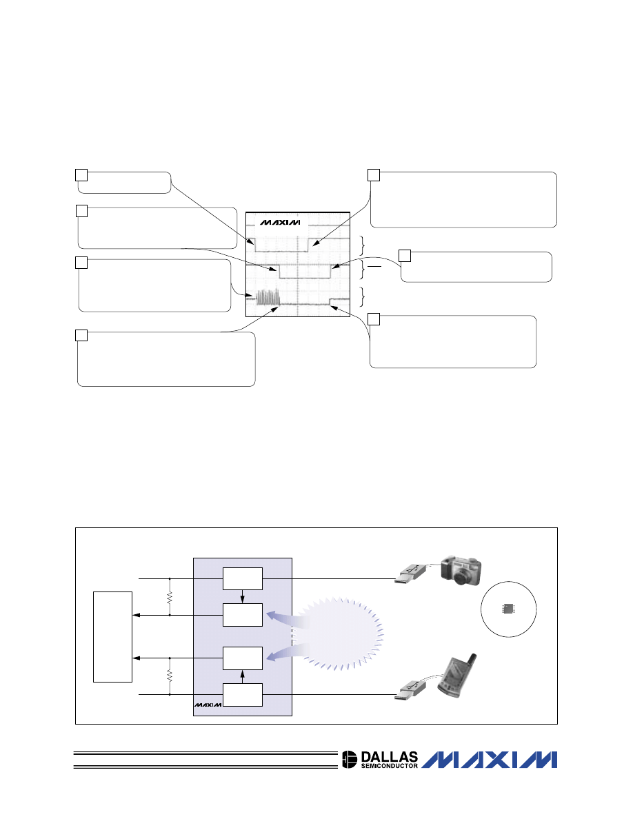
22nd EDITION
4
4
POWER SUPPLIES
ANALOG
DESIGN GUIDE
Data Sheets
Applications Notes
Free Samples
•
•
ANALOG
DESIGN GUIDE
1
2
3
4
5
6
7
8
9
10
11
Multiplexers, Switches
DC-DC Converters,
Power Supplies
High-Speed
ADCs & DACs
Signal Conditioners
Video/High-Speed Amps
Interface Products
Op Amps, Comparators
µP Supervisory
Analog Filters
A/D Converters
D/A Converters
Analog Functions
Voltage References
Temperature Sensors
12
13
14
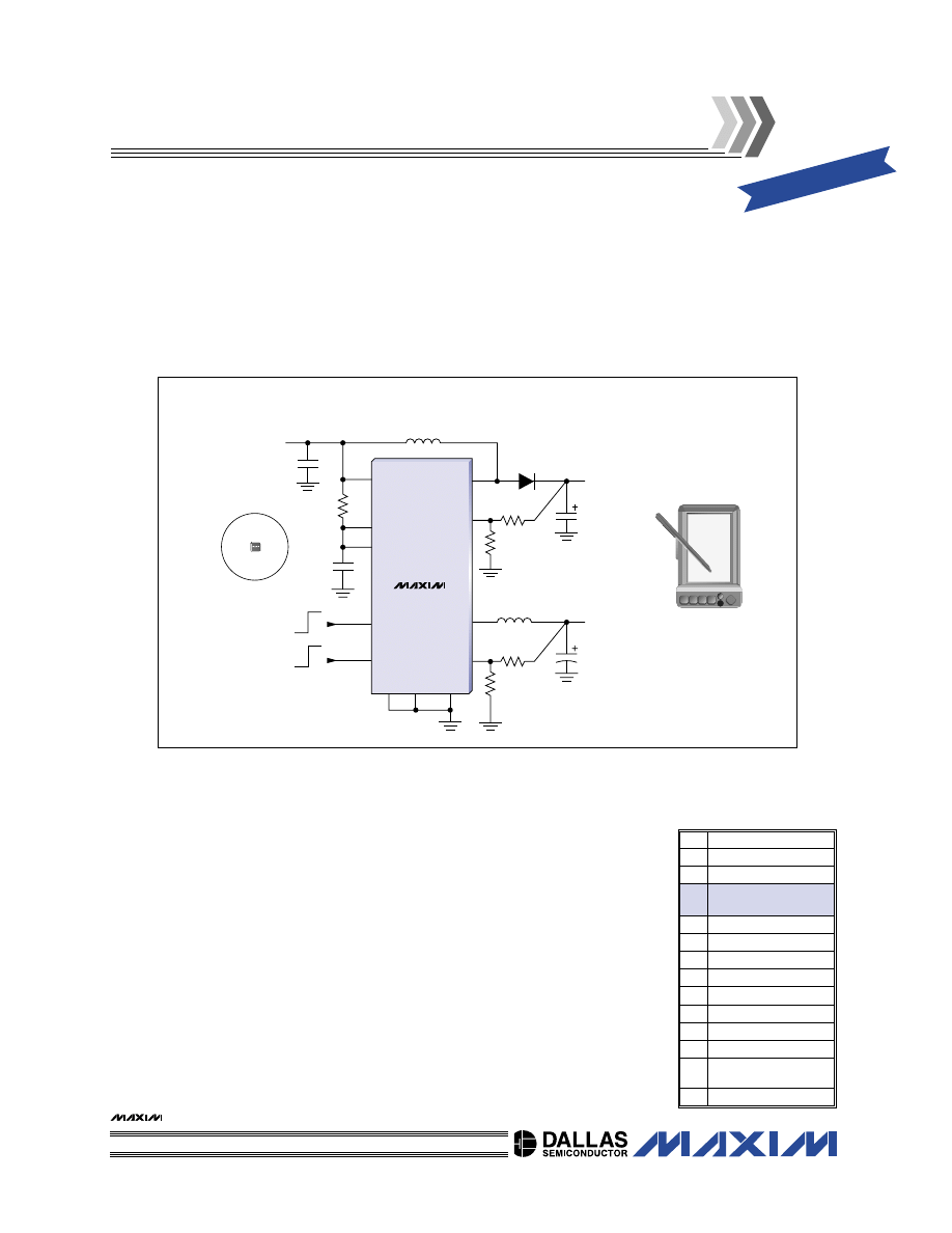
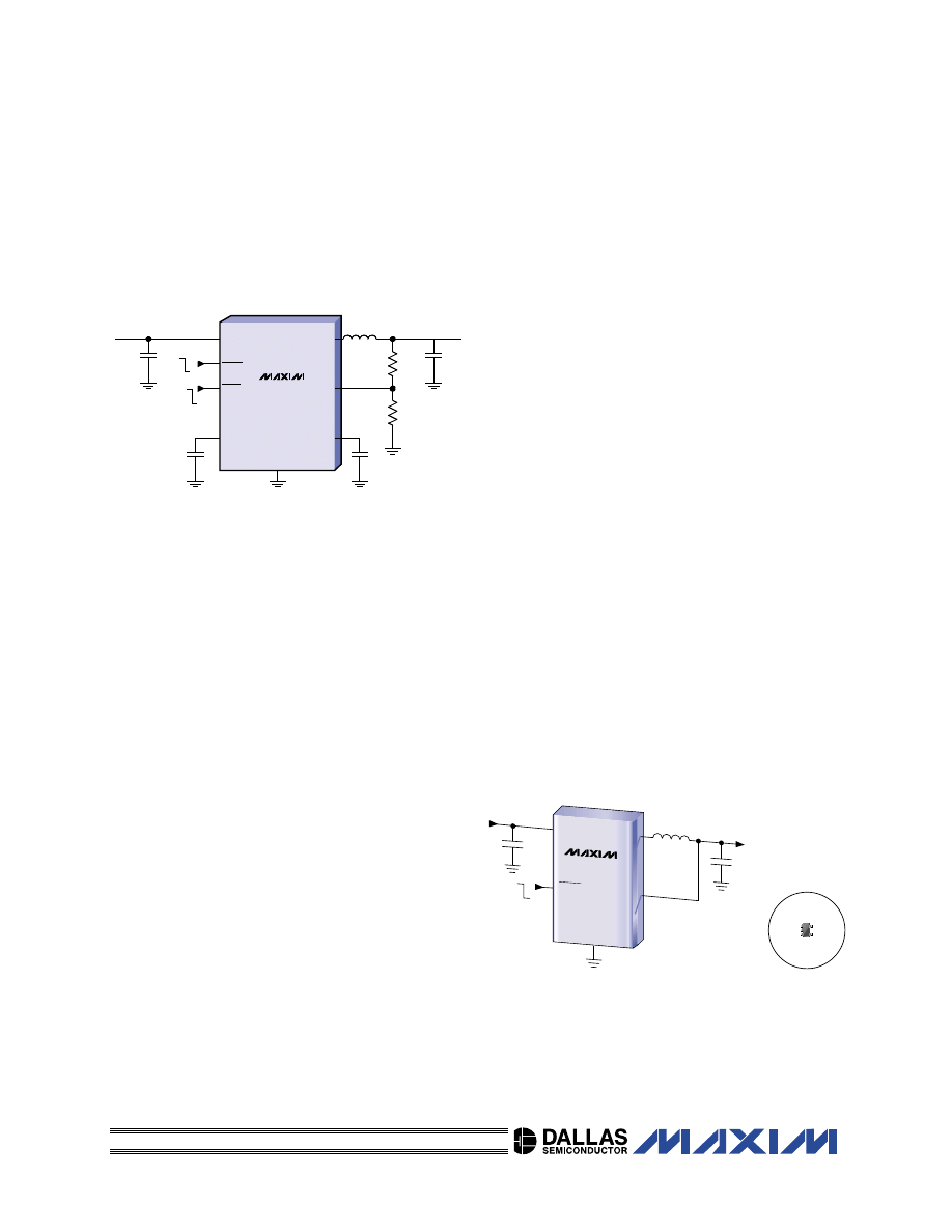
Smallest Dual-Output Supply
for PDAs: Logic Step-Down and
LCD Step-Up
High-Efficiency Hand-Held Supply Fits Internal Switches into a
12-Pin QFN Package
• Dual-Output:
• Step-Down: Logic Supply Down
to 1.25V
• Step-Up: LCD Supply Up to 28V
• Smallest Package: 4mm x 4mm
12-Pin QFN
• Small External Components:
10µF and 10µH
• 90% Efficiency
• Low 19µA Quiescent
Supply Current
• Evaluation Kit
Available to Speed
Designs
• Priced at $1.57
†
MAX1878
PGND AGND
INPUT
2.0V TO 5.5V
PGNDLCD
10
µH
10
µH
ON
OFF
FB
LX
FBLCD
LXLCD
AIN1
AIN2
IN
ONLCD
ON
ON
OFF
LOGIC
LCD
LOGIC OUTPUT
1.25V TO V
IN
UP TO 500mA
0.1
µF
LCD OUTPUT
UP TO 28V
UP TO 10mA
4
m
m
x
4 m m x 0
.8
5
m
m
12
-PIN QFN
Packaged in a 0.85mm high, 4mm x 4mm QFN, the MAX1878 is the
simplest and smallest single-chip solution providing both logic and LCD
power for PDAs and hand-held products. For the logic supply, it uses a
high-efficiency (90%) step-down DC-DC converter with synchronous rectifi-
cation that eliminates the need for an external diode, saving cost and size.
For the LCD supply, the internal switch is capable of supplying outputs as
high as 28V. Each output has its own logic-controlled enable.
†1000-up recommended resale. Price provided is for design guidance and is FOB USA. International prices will differ due to local duties,
taxes, and exchange rates. Not all packages are offered in 1k increments, and some may require minimum order quantities.
STEPS DOWN TO 1.25V FOR NEWEST LOGIC CHIPS
is a registered trademark of Maxim Integrated Products, Inc. © 2002 Maxim Integrated Products.
P
V
IN
V
IN
N
N
V
IN
N
MAX1801
V
IN
N
ON
OFF
OUT1
LDO
OUT2
STEP-UP
MASTER
OUT3
OUT4
OSC
REF
GND
OUT1 ON
OUT2 ON
OUT3 ON
OUT4 ON
LDO ON
MAX1800
INPUT
0.7V TO 5.5V
3.3V
EIGHT OUTPUTS
1.8V
7.0V
15.0V
-7.5V
18.0V
12.0V
5.0V
LOGIC
CORE
CCFL MODULE
CCD BIAS
LCD BIAS
ZOOM
MOTOR DRIVE
(OPTIONAL)
N
P
DL
OSC
SLAVE
CONTROLLER
REF
MAX1801 SLAVE CONTROLLER
8-PIN SOT23
2.8mm x 2.9mm
32-PIN TQFP—5x5*
7mm x 7mm x 1mm
(DIMENSION INCLUDES LEADS)
MAX1800 STEP-UP MASTER
MAX1802 STEP-DOWN MASTER
MAX1801
V
IN
N
5.0V LENS COVER
DRIVE
(OPTIONAL)
DL
OSC
REF
ADD UP
TO FIVE SLAVE
CONTROLLERS
SLAVE
CONTROLLER
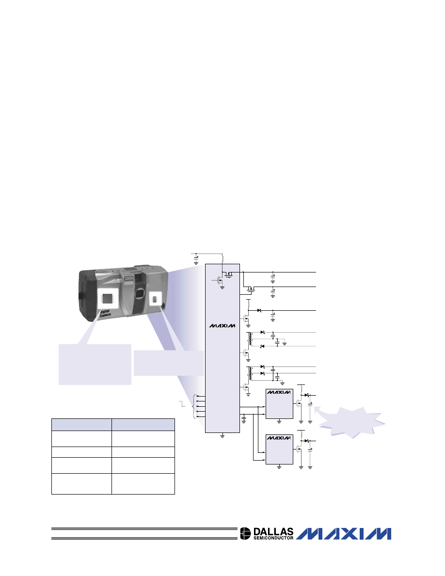
Smallest, Highest Efficiency
Multi-Output DC-DC Converter
Compact, Cost-Effective, Integrated Power Supply Solutions for
Digital Cameras and PDAs
Use the MAX1800 step-up master or the MAX1802 step-down master to provide all the voltage
outputs required in your digital camera and PDA designs from a single IC. They include high-effi-
ciency DC-DC converters with synchronous rectifiers to give over 90% efficient power conversion for
the logic supply, which uses >50% of the power in a camera system. They come in a small 32-pin
5mm x 5mm TQFP, which is 40% smaller than existing TQFP solutions. The MAX1800 and MAX1802
also eliminate external components such as power diodes, power switches, and at least one
transformer to save cost and size. For flexibility, add the low-cost, 8-pin SOT23 MAX1801 “slave”
controller to create optional features like a motor control supply for zooming and focusing. The
MAX1800/MAX1802 can provide all the voltages for logic, core, backlighting, LCD, and expansion
port of PDAs.
EXAMPLE OF A COMPLETE DIGITAL CAMERA POWER SUPPLY
(CAN ALSO BE USED IN PDAs)
MAX1800
MAX1802
Step-Up,
Step-Up/Down
Step-Down
0.7V to 5.5V Input
2.5V to 11V Input
One Li+,
Two or Three Alkaline
Two Li+,
Four Alkaline
Internal Step-Up,
Three Step-Up Controllers,
LDO Controller
Step-Down Controller,
Three Step-Up Controllers,
Internal Step-Down
1-, 2-, 3-, or 4-Cell Designs
*Dimensions include 5mm body plus 1mm for the length of each lead for a total of 7mm.
Lowest Cost Three- and Five-Output
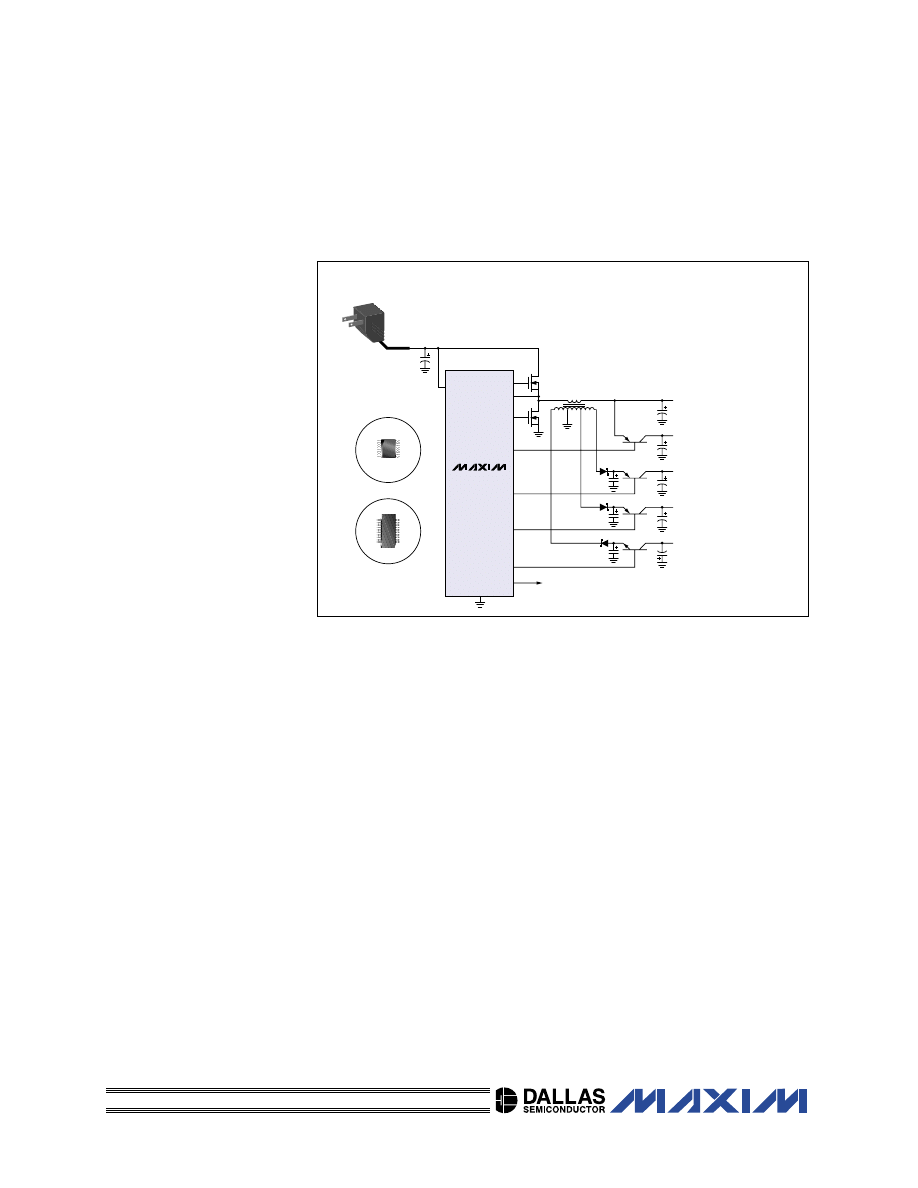
xDSL and Cable Modem Power Supplies
High-Efficiency Step-Down Controller Plus Multiple LDO Controllers
on a Single IC
LDO4
POK
LDO2
LDO3
LDO1
DL
DH
N
N
GND
POWER OK
SIGNAL
V+
INPUT
LOW-COST
ADAPTER
4.5V TO 28V
3.3V
1A
FIVE OUTPUTS
2.5V
500mA
5V
100mA
12V
100mA
POSITIVE
LINE DRIVER
-12V
100mA
NEGATIVE
LINE DRIVER
I/O
CORE
AFE
MAX1865T
COMPLETE, LOW-COST, FIVE-OUTPUT xDSL MODEM SUPPLY
6
m
m
x 8.65
m
m
20
-PI
N QSO
P
6
m
m
x 4.9 m
m
16
-PI
N QSO
P
1864
1865
MAX1864
• Step-Down Controller
• Two Positive LDO Controllers
• 16-Pin QSOP Package
MAX1865
• Step-Down Controller
• Three Positive LDO Controllers
• One Negative LDO Controller
• 20-Pin QSOP Package
• No Current-Sense
Resistors Mean
Less Cost
• Step-Down Output:
1.25V to 5.5V
• LDO Outputs:
±1.25V to ±15V
• Power-OK Checks All
Outputs
• EV Kit Available to
Speed Designs
Use the MAX1864 and MAX1865 power-supply controller ICs to build the lowest cost xDSL and
cable modem consumer premises equipment (CPE) power supplies. They integrate a high-efficiency
step-down DC-DC controller and two to four linear regulator controllers that provide all the required
voltages for CPE. The current-mode step-down controller uses an external, dual N-channel MOSFET to
provide low-cost synchronous rectification for high efficiency and low heat. To further save cost, no
external current-sense resistor is required. Switching frequencies of 100kHz and 200kHz permit the
use of low-cost magnetics and aluminum electrolytic capacitors. The linear regulator controllers drive
inexpensive external bipolar junction transistors (B JTs).
110V Power Supply Controller
Integrates High-Voltage Startup FET
• Up to 300kHz Operation for Smaller
Magnetics and Capacitors
• Wide 11V to 110V Input Voltage Range
• Guaranteed ±2.5% V
REF
Accuracy
• Only 2.2mA Supply Current
• Input Feed-Forward
Compensation for Fast Line-
Transient Response
• Programmable: Current
Limit, Maximum Duty
Cycle, Oscillator
Frequency, Undervoltage
Lockout, and Soft-Start
• External Frequency Synchronization
• MAX5003 EV Kit Available to Speed
Designs
V
IN
V
IN
(UP TO 110V)
V
CC
R
SENSE
N_DRV
CS
V
OUT
5V
OPTOCOUPLER
FEEDBACK
MAX5003
HV PWM
CONTROLLER
ISOLATION
INTERNAL
110V STARTUP
TRANSISTOR
16
-PI
N QSO
P
4
.8
0m
m x 5.84
m
m
43% SMALLER FOOTPRINT
THAN COMPETITOR’S SO-14
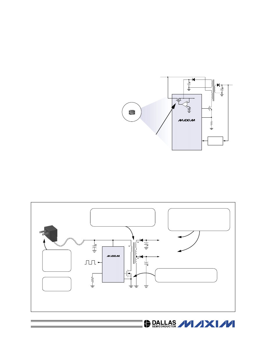
Low-Cost, Dual-Output SLIC Supply
Uses Standard Transformer
EXT
GND
FREQ
N
SYNC
SYNC SIGNAL
(OPTIONAL)
FREQUENCY
SELECT
(100kHz TO 500kHz)
V
CC
INPUT
8V TO 24V
OUTPUT 1
-72V, 100mA RING BATTERY
OUTPUT 2
-24V, 400mA TALK BATTERY
OUTPUT VOLTAGE CAN BE SET
TO OPTIMIZE SHORT-LOOP OR
LONG-LOOP OPERATION WITH
VARIOUS SLIC ICs
FLYBACK TOPOLOGY REDUCES
INPUT RIPPLE CURRENT
STANDARD TRANSFORMER FROM
MULTIPLE VENDORS
REDUCES COST
LOW-COST
UNREGULATED
AC-DC
ADAPTER
DIGITAL
SOFT-START
MAX1856
EVALUATION KIT AVAILABLE TO SPEED DESIGNS. The MAX1856 can be configured to work with different input and
output voltages from those shown in this block diagram. For further information, please contact your local Maxim FAE or email us
at powerhelp@design.mxim.com.
Optimized for Telecom and
Data Communications Applications
MAX5910
MAX5917
BACKPLANE
(+10V TO +65V)
N.C.
PGOOD
FAULT
GND
V
OUT
ENABLE
UVLO
V
IN
DATA TERMINAL EQUIPMENT
• IP Phone
• Wireless LAN Access Node
(Eliminates AC Adapter)
• Security Camera
(Eliminates AC Adapter)
SAFELY CONNECT YOUR
DATA TERMINAL EQUIPMENT
TO A SWITCH/ROUTER
POWER SOURCE.
Part
MAX5910
MAX5917A
MAX5917B
Output Current Limit
(mA)
280
567
420
Pin-Package
8-SO
16-SO
16-SO
V
IN
UVLO
-16V to -65V
FAULT OUTPUT
ON/OFF
DGND
GATE
V
OUT
AGND
WITHSTANDS
-70V TRANSIENTS
MONITORS UVLO
POWER NOT GOOD,
LOAD DISCONNECT
& THERMAL SHUTDOWN
COMPATIBLE WITH
3.3V AND 5V LOGIC
ADJUST DEFAULT
UVLO THRESHOLD
WITH EXTERNAL
RESISTOR DIVIDER
CAN VARY
±5V
WITH RESPECT
TO AGND
♦ 2Ω INTERNAL POWER
SWITCH
♦ DELIVERS 13W POWER
(20W FOR MAX5912)
♦ DISCONNECTS LOAD AT
“ZERO CURRENT”
♦ SAFE HOT SWAP
MAX5911/
MAX5912
SIMPLE
SWAPPER™
Beats Competition 3 Ways
65V SWITCH IS IEEE802.3af COMPATIBLE
-48V SWITCH DELIVERS POWER AND DATA OVER
STANDARD CATEGORY 5 CABLE
Industry’s First Hot-Swap Switches
for Power-Over-LAN
Simple-Swappers™ Require No Design and No External Components
Simple-Swapper is a trademark of Maxim Integrated Products, Inc.
1) First IEEE802.3af-Compatible
Hot-Swap Switch
• Drives 500µF at Startup
• 500mA Output Current at
Startup
• Input Voltage Range:
+10V to +65V
2) Highest Integration
• Internal Switch Delivers 26W
of Power
• Built-In Undervoltage Lockout
(UVLO)
• Power Good Output Monitors:
UVLO, Power Not Good, and
Thermal Shutdown
3) Smallest Board Space and
Lowest Cost
• Requires No External
Components
• 60% Less Board Space than
Discrete Solutions
• 8-Pin or 16-Pin SO Packages
MAX5911
280
8-SO
MAX5912
415
16-SO
Highest Power Step-Up DC-DC
Delivers 20W to Replace Modules
Drop-In, Internal Switch 20W PWM Design in SO Package
ON
600kHz OR
SYNCHRONIZABLE
INPUT
0.7V to 5V
PROGRAMMABLE
CURRENT LIMIT
AND SOFT-START
OFF
OUTPUT
5V/4A
LOCAL
POWER BUS
1
µH
NETWORK OR TELECOM CARD
LOCAL ISOLATED
3.3V POWER BUS
MAX1709
MAX1708
16-PIN QSOP
5A MOSFET
16-PIN NSO
MAX1709
9A MOSFET
28-PIN QSOP
RACK-MOUNTED
TELECOMMUNICATIONS
SYSTEM
V
CC
INPUT
2.5V TO 5.5V
POWER INPUT
1V TO V
OUT
ON
OFF
FB
GND
EXT
SIMPLEST AND SMALLEST BOOST CONTROLLER CIRCUIT
ELIMINATES INRUSH CURRENT
OUTPUT
>V
IN
UP TO
30W
Built-in soft-start eliminates inrush current spikes, permitting use of a smaller and lower
cost input capacitor and inductor. The costly sense resistor is also eliminated.
V
CC
SHDN
N
2
.9
m
m x 2.8
m
m
6-
PIN
SOT2
3
400
µs/div
SOFT-START RESPONSE
V
IN
= 3V
V
OUT
= 12V
R
LOAD
= 200
Ω
I
LOAD
= 60mA
V
OUT
,
5V/div
I
L
, 1A/div
V
SHDN
, 5V/div
MAX1522
MAX1523
MAX1524
Simplest SOT23 Step-Up Controllers
Use Fewest Components
Use the MAX1522/MAX1523/MAX1524 DC-DC controllers to build the simplest and smallest
step-up circuits. These SOT23 controllers have an internal digital soft-start that eliminates the inrush
current spikes that shorten useful battery life. Soft-start also permits a smaller input capacitor. These
controllers eliminate the sense resistor to increase efficiency while saving space and cost. Finally, they
switch at up to 1MHz, permitting the use of a small inductor.
The MAX1708 and MAX1709 set a new standard of space savings for high-power step-up DC-DC
conversion. The MAX1709 packs a 22m
Ω, 9A, power MOSFET into a small SO package. It operates
from inputs in the 0.7V to 5V range, and provides up to 20W at fixed (3.3V or 5V) or adjustable (2.5V
to 5.5V) voltages. For lower power applications, choose the MAX1708, which provides up to 10W (5V at
2A) in a smaller 16-pin QSOP package. For added flexibility, both devices include programmable soft-
start and current limit, allowing external components to be optimized when less than full-power
capability is required.
1.5W
PACKAGE
OUTPUT
UP TO 5.5V
UP TO 500mA
1 x Li+
OR
2AA
INPUT
INPUT
INPUT
SMALLEST PACKAGE
ON
OFF
GND
ON
LX
OUT
OUTPUT
3.3V
UP TO 500mA
1 x Li+
2.5V TO
4.2V
STEP-UP/DOWN
ON
OR
OFF
GND
ON
LX
OUT
CORE POWER
3.3V OR 1.5V
UP TO 1.5A
DUAL OUTPUTS
SYSTEM POWER
5V OR 3.3V
UP TO 1.5A
1 x Li+
OR
2AA
HIGHEST POWER
ON
OFF
ON
DC/DC
LDO
OFF
GND
LX
INL
DC/DC OUT
FB
LDO DR
3
m
m
x
4.9mm x 1
.1
m
m
10
-PIN µMAX
4
.9
m
m
x 6mm x 1
.7
m
m
16
-PIN QSOP
5
m
m
x 6.3
m m x
1.
1m
m
16
-P
IN T
SSOP
-EP
1.5W
PACKAGE
OR
4
.9
m
m
x 6mm x 1
.7
m
m
16
-PIN QSOP
5
m
m
x 6.3
m m x
1.
1m
m
16
-P
IN T
SSOP
-EP
MAX1760
MAX1763
MAX1765
Highest Power, Low-Voltage, Boost
DC-DCs Are Now Smaller
50% Smaller Packages, 0.7V Startup Voltage, Up to 1.5A Output,
1MHz Switching (or Synchronize from 500kHz to 1.25MHz)
The MAX1760/MAX1763/MAX1765 are 50% smaller upgrades to the popular MAX1700 family of
low-voltage, high-power, high-efficiency PWM step-up DC-DC converters. The MAX1760 family
features smaller external components, adjustable current limit, and soft-start. They deliver more
power from low voltages than any other step-ups available: 1.5A from 3.6V
IN
(single Li+) and 400mA
from 1.2V
IN
(single NiMH or alkaline). Input range is 0.7V to 5.5V. Switcher output range is 2.5V to
5.5V. The MAX1763 and MAX1765 include a linear regulator for a second output.
EVALUATION KIT AVAILABLE TO SPEED DESIGNS. Conceptual schematics; not all components are shown.
Regulated Step-Up/Down Charge
Pump Delivers Guaranteed 125mA
OUT
IN
SHDN
GND
CXN
CXP
MAX1595-33
MAX1595-50
0,22
µF
1
µF
1
µF
4
m
m
x 4mm x
1m
m
12
-PIN QFN
5
m
m
x
3,1mm x
1,
1
m
m
8-
PIN µMAX
EINGANG
1,8V
BIS
5,5V
AUSGANG
5V ODER 3,3V
125mA
ON
OFF
ODER
1,48W
Verlustleistung
€1,69*
Preisgünstig mit
0,36W Verlustleistung
€1,60*
GEREGELTE AUFWÄRTS-/ABWÄRTS-
WANDLUNG MIT 1 KONDENSATOR
WÄHLEN SIE
LEISTUNG ODER
PREIS
INPUT VOLTAGE (V)
OUTPUT VOLTAGE (V)
0
1.0
2.0
3.0
4.0
5.0
6.0
0
1.0
2.0
3.0
4.0
5.0
6.0
V
OUT
= 5.0V, I
LOAD
= 125mA
V
OUT
= 3.3V, I
LOAD
= 75mA
NO INDUCTOR, ALL CERAMIC CAPACITORS
STEP-UP/DOWN REGULATION
†1000-up recommended resale. Price provided is for design guidance and is FOB USA. International prices will differ due to local duties, taxes, and exchange rates.
Delivers 5V or 3.3V from a 1.8V to 5.5V
Input with No Inductors
OPEN
D+
V
BUS
V
CC
RST
D+
D-
D-
GND
MAX5005
MAX5006
MAX5007
USB PORT
ENABLE
RESET
SELR
LDO
REGULATOR
1.5k
Ω
5V
3.3V
1
µF
CERAMIC
SUPERVISORY
INTERNAL D+ AND D- TERMINATION
RESISTOR AND CONTROL
♦ USE SELR PIN TO CONFIGURE USB
PERIPHERAL FOR FULL SPEED OR
LOW SPEED
♦ USE ENABLE PIN TO DESELECT INTERNAL
TERMINATION RESISTOR
µP RESET CIRCUIT
♦ ENABLES USB CONTROLLER
WHEN V
OUT
IS IN
REGULATION
♦ 200ms TIMEOUT PERIOD
LOW QUIESCENT CURRENT LDO REGULATOR
♦ 3.3V/150mA OUTPUT
♦ 30µA SUPPLY CURRENT INDEPENDENT OF LOAD
♦ STABLE WITH 1µF CERAMIC OUTPUT CAPACITOR
ROBUST TRANSIENT VOLTAGE
SUPPRESSORS FOR DATA LINES
♦ IEC 1000-4-2 AIR DISCHARGE
VOLTAGE TO
±15kV
♦ IEC 1000-4-2 CONTACT DISCHARGE
VOLTAGE TO
±8kV
♦ 6A SURGE CURRENT RATING
3.3V USB
CONTROLLER
New! Schematics and Bills of
Materials Online
Choose Proven, Lab-Tested Circuits from Maxim’s Growing Library of
Applications
Maxim has placed over 30 useful power-supply application circuits on our website for you to
browse and download. You can sort the list by topology, input voltage, or output voltage and download
schematics and component bills of materials, including part numbers and vendor names. You can also
submit an application for an evaluation board to be built for you. Check the list often for new
additions. Visit http://dbserv.maxim-ic.com/PowerSupplies.cfm
Topology
Step-Down
Step-Up
Inverter
Input Voltage
(V)
5
2.5
3.3
Output Voltage
(V)
1.2
5
-5.2
Key Attributes
Tracking supply for DDR termination
Internal switch, smallest size, synchronization
<3mm profile, very low ripple
Schematic and
Bill of Materials
Download
Download
Download
Evaluation
Board
Request
Request
Request
Multi-Output
12
3.3, 2.5, 1.8, -4.8
Low-cost, single controller design
Download
Request
Output Current
(A)
6
3
0.3
1, 0.3, 0.2, 0.06
Request
Evaluation
Board
Download
Schematic and
Bill of Materials
Sort By
Output
Current
Sort By
Input
Voltage
USB Power Management IC
Integrates ±15kV Transient
Voltage Suppressors
Highest Integration Saves Board Space, Cost, and Design Time, Fits
in a 10-Pin µMAX Package
Push-Pull Active High
MAX5007
Push-Pull Active Low
MAX5006
Open Drain
MAX5005
Reset Output
Part
t = 10ms/div
SHORT-CIRCUIT
FAULT RESPONSE
5V, V
IN
5V
0
5V
0
1A
0
V
OUT
FAULT
INDICATOR
I
OUT
1
SHORT APPLIED
2
FAULT INDICATOR
TRIPS AFTER 20ms BLANKING
TO PREVENT HOT-SWAP GLITCHES
3
FAULT-CONDITION
CURRENT LIMITED TO 350mA
RMS
BY PULSING (COMPETITOR'S
CURRENT SHOOTS TO I
SHORT
)
4
SWITCH TURNS ITSELF OFF
AFTER 20ms (COMPETITION WAITS
FOR MICROPROCESSOR SIGNAL,
WASTING POWER & RISKING DAMAGE)
5
SHORT-CIRCUIT REMOVED AND
AUTOMATICALLY DETECTED BY MAX1823
(COMPETITION REQUIRES DETECTION
CIRCUIT & MANUAL POWER RECYCLING)
6
20ms RESET SIGNAL ALLOWS
PROPER SYSTEM START-UP
7
SWITCH TURNS ITSELF ON 20ms
AFTER DETECTING FAULT REMOVAL
(COMPETITION REQUIRES MICRO-
PROCESSOR SIGNAL)
MAX1823
Smart Dual USB Switch Reduces
Software Overhead with
Auto Turn-Off/-On
World’s Smallest, Dual, Current-
Limited Switch with Fault-Blanking
The MAX1812 is the world’s smallest, dual, current-limited switch for USB applications. Each
channel is guaranteed to supply 500mA and meets all USB specifications. Internal fault-blanking
prevents momentary faults (capacitive loads) from resetting the host system and eliminates the need
for external components.
INTERNAL FAULT-BLANKING SAVES COMPONENTS AND PREVENTS HOT-SWAP GLITCHES
500mA
SWITCH
INA
5V
5V
OUTA
FAULTA
20ms
DELAY
20ms
DELAY
FAULTB
OUTB
TO USB
PORT A
TO USB
PORT B
INB
500mA
SWITCH
HOST
µP
INTERNAL
BLANKING
ELIMINATES FOUR
EXTERNAL
COMPONENTS
MAX1812
3
m
m
x
4.9mm x 1
.1
m
m
10
-PIN µMAX
AREA = 2.95mm x 4.9mm
HEIGHT = 1.11mm, MAX
OUTPUT
3.3V/5V
UP TO 4A
22
µH
220
µF
40m
Ω
0.1
µF
4.7
µF
4.7
µF
47
µF
VL
REF
CS
EXT
OUT
V+
VH
MAX1744
INPUT
4.5V TO 36V
SHDN
OFF
ON
GND
36V Input, 20W Output Step-Downs
Save Space
NEW
100
0
0.0001
0.001
0.01
0.1
1
10
EFFICIENCY vs. LOAD CURRENT
(V
OUT
= 5.0V)
20
LOAD CURRENT (A)
EFFICIENCY (%)
40
60
80
A: V
IN
= 7.2V
B: V
IN
= 12.0V
C: V
IN
= 24.0V
D: V
IN
= 36.0V
B
A
D
C
• High-Voltage Operation
(Up to 36V
IN
)
• 10-Pin µMAX Package
• Up to 330kHz Switching
Frequency Reduces
Component Sizes
• Output Power >20W
• High Efficiency
• 90µA Quiescent Supply
Current
• 4µA Shutdown Current
• Output Voltage: 3.3V/5V
(MAX1744) Adj. 1.25V to
18V (MAX1745)
DIRECT STEP-DOWN FROM 24V WITHOUT 2-STAGE EFFICIENCY LOSS
AUDIO
RTC
WLAN
VIDEO
I/O
P
INTERNAL
24V P-CHANNEL
MOSFET
DIRECT CONVERSION
FROM 4.5V TO 24V
(FOUR Li+ OR AC-DC
ADAPTER)
I
Q
= 12
µA
MAX1776
I
Q
= 15
µA
500mA
8-PIN
µMAX
OUTPUT
1.25V TO V
IN
UP TO 500mA
90% EFFICIENCY
MAX1836/MAX1837
125mA/250mA
6-PIN SOT23
MAX1836
Smallest Step-Down Converter with
24V Internal MOSFET Switch
3-/4-Cell Li+ Powered, Low I
Q
, Keep Alive, and Wake-On LAN Supply
The MAX1837 delivers up to 250mA, the MAX1836 delivers up to 125mA, and the MAX1776
delivers up to 500mA, permitting optimal inductor selection. The MAX1836/MAX1837 come in a 6-pin
SOT23 package, and the MAX1776 comes in an 8-pin µMAX package. Both convert directly from 24V
inputs, eliminating the intermediate step-down voltage that wastes over 15% of the battery life and
increases complexity. Applications include I/O, audio, keep-alive, WLAN, and video supplies in
notebook and hand-held systems powered by up to four lithium batteries and AC-DC adapters.
3
m
m x 5m
m
10
-PI
N
µM
AX
Direct conversion from 24V to 3.3V saves 15% power by eliminating compound efficiency losses generated when converting
from 24V to 5V and then from 5V to 3.3V.
Smallest 250mA Step-Downs Achieve
95% Efficiency for Sub-2V Logic
1MHz, 600mA Step-Down Powers DSP
Cores Using Inexpensive Capacitors
The MAX1821 is the first 1MHz PWM converter capable of delivering precision line and load regu-
lation for the latest DSP cores using low-ESR ceramic input and output capacitors. The precision line
and load regulation is achieved through an innovative current-mode control algorithm. Its unique
slope compensation and high-bandwidth error amplifier, combined with a simple external compensa-
tion circuit, stabilize the converter with only a small 4.7µF ceramic capacitor. The MAX1821
can operate in PWM or PFM mode to maximize standby and operational efficiencies. To maximize
battery life, the MAX1821 delivers > 93% efficiency using an integrated low R
DSON
switch and synchro-
nous rectifier.
LX
BATT
FB
COMP
SHDN
SKIP
PWM
PFM
MAX1821
4.7
µH
4.7
µF
GND
INPUT
2.5V to 5.5V
OUTPUT 1.8V AT 600mA
ADJUSTS DOWN TO 1.25V
ON
OFF
REF
4.7
µF
• 600mA Guaranteed Output
Current
• 1MHz PWM Switching Frequency
• Requires only 4.7µF Ceramic
Capacitor
• Excellent Line and Load Regulation
• Synchronize to 2.5G (19.8MHz)
or 3G (13MHz) System Clock
• Programmable Output Voltage
from 1.25V to 5.5V
• No Schottky Diode Required
High-Speed Converter Provides Excellent Line and Load Regulation
Using Tiny, 4.7µF Ceramic Capacitors Instead of Expensive, High-
ESR Tantalum Capacitors
The MAX1733/MAX1734 step-down DC-
DC converters deliver over 250mA to outputs
as low as 1.25V and have 1.5% output voltage
accuracy. The input voltage range of 2.7V to
5.5V makes these devices ideal for portable
applications powered from a single lithium cell,
from three alkaline or NiCd/NiMH cells, or
from a regulated 3.3V or 5V supply.
These converters use a unique proprietary
current-limited control scheme that maintains
a low 40µA quiescent supply current, while
their high 1.2MHz (max) switching frequency
and internal synchronous rectification significantly improve efficiency and minimize solution size. This
reduces external component size and eliminates the external Schottky diode required with conven-
tional step-down converters. Only three small external components are needed for a complete DC-DC
solution.
The MAX1733 provides a resistor-adjustable output voltage, while the MAX1734 is available in a
variety of preset output voltages. Both devices are available in space-saving 5-pin SOT23 packages.
OUTPUT
1.25V TO 2.5V (MAX1733)
1.5V OR 1.8V (MAX1734)
UP TO 250mA
10
µH
SHDN
IN
GND
OUT
LX
MAX1734
INPUT
2.7V TO 5.5V
OFF
ON
5-
PIN
SOT2
3
3
m
m x 3m
m
4.7
µH
RF RECEIVE SECTION
V
OUT
CONTROL
DAC
13MHz OR 18MHz
SYSTEM CLOCK
BASEBAND
PROCESSOR
4.7
µF
LX
OUT
REF
GND
SYNC
MAX1820
BATT
RF TRANSMIT SECTION
2.5G AND 3G
FIXED-GAIN
LINEAR PA
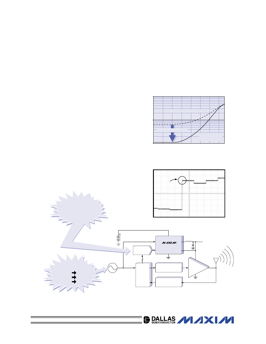
OUTPUT OF HIGH-SPEED DC-DC
TRACKS PA POWER ENVELOPE WITHIN 30
µs
1000
100
10
-10
-5
0
5
10
TRANSMIT POWER (dBm)
15
20
25
BA
TTER
Y CURRENT (mA)
SAVE 83% BATTERY CURRENT
PA CONNECTED
TO MAX1820
PA CONNECTED TO BATTERY
REDUCE BATTERY CURRENT
FROM 62mA TO 11mA
DATA MODE
400
µs/div
PA SUPPLY
VOLTAGE
FAST 30
µs
SETTLING TIME
VOICE MODE
DYNAMIC OUTPUT
0.4V TO 3.4V IN 30
µs
UP TO 600mA
INPUT
2.7V TO 4.2V
CLOCK SYNC
REDUCES NOISE
MAX1820Z
MAX1820Y*
MAX1820X*
NO SYNC
÷ 18 PLL
÷ 13 PLL
ONLY SUPPLY WITH
DAC INPUT FOR DIRECT
COMMUNICATION
FROM BB PROCESSOR
Li+ BATTERY
500mV/div
Reduce WCDMA PA Current Draw
83% with Dynamically Controlled
Step-Down DC-DC
High-Speed DC-DC Adjusts 2.5G and 3G PA Supplies to Match
Transmit Power
The MAX1820 is the first step-down
converter designed specifically for PAs in 2.5G
and 3G cellular phones. The baseband
processor dynamically programs the converter
output voltage based on the variable power
required by the PA. The high-speed MAX1820
converter varies its output voltage from 0.4V to
3.4V in less than 30µs, tracking the PA transmit
power envelope. By matching the PA supply
voltage envelope, the PA minimizes power loss
and maximizes battery life. The MAX1820 is
equipped with a divide-by-13 or
divide-by-18 phase-locked-loop (PLL) to
synchronize to a 2.5G or 3G system clock. An
actual test with a WCDMA PA proved this
synchronization method does not add spurious
noise into the RF band.
*Future product—contact factory for availability.
ON
INDEPENDENT
CONTROLS
EN1
OUT1
2.2
µF
4.7
µF
IN1
OFF
IN2
IN3
2.2
µF
2.2
µF
OUT3
OUT2
EN3
EN2
BP
GND
0.01
µF
Li+
BATTERY
INPUT
2.5V TO 5.5V
3 OUTPUTS
1.8V TO 3.3V
100mA
1.8V TO 3.3V
100mA
1.8V TO 3.3V
100mA
MAX8890
CERAMIC INPUT AND
OUTPUT CAPACITORS
SAVE COST
FACTORY PRESET
OUTPUTS SAVE
SPACE
100
1000
0
10
20
30
40
60
50
80
70
0.1
1
10
67dB POWER-SUPPLY
REJECTION RATIO
FREQUENCY (kHz)
PSRR (dB)
C
IN
= 1
µF + 0.1µF
I
OUT
= 10mA
100
1000
0
100
10
1000
0.1
1
10
LOW-CROSSTALK VOLTAGE
FREQUENCY (kHz)
CROSSTALK (
µ
Vp-p)
LOW-IMPEDANCE INPUT
I
OUT1
= 100mA SINUSOIDAL LOAD
I
OUT3
= 10mA
4
m
m
x
4 m m x 0
.8
5
m
m
12
-PIN QFN
Triple, Low-Noise, Low-Dropout
Linear Regulators Provide Complete
RF Power
67dB PSRR, Low-Crosstalk Voltage, and 45µV
RMS
Noise Provide
Flawless Transmission
The MAX8890 contains three identical 100mA, low-noise linear regulators in a low-profile 4mm x
4mm x 0.85mm QFN package. Their 67dB PSRR, low-crosstalk voltage, and 45µV
RMS
noise make
them ideal for the noise-sensitive RF sections of cellular phones and wireless PDAs. Low 50mV
dropout at 100mA load maximizes battery life. Output voltages are preset from 1.8V to 3.3V in 50mV
increments. The MAX8890 is priced at $0.99
†
.
3 LOW-NOISE LDOs IN A SINGLE QFN PACKAGE
†1000-up recommended resale. Price provided is for design guidance and is FOB USA. International prices will differ due to local duties, taxes, and exchange rates.
OFF
ON
SHDNB
UP TO 160mA
1.8V TO 3.3V
UP TO 160mA
1.8V TO 3.3V
DUAL
OUTPUTS
IN
GND
OUTA
OUTB
MAX8883
INPUT
2.5V TO 5.5V
OFF
ON
SHDNA
INCREDIBLE 1.0
Ω
MOSFET PASS SWITCHES
UP TO 160mA
FROM EACH OUTPUT
80
0
0.01
0.1
1
10
100
1000
PSRR VS. FREQUENCY
10
20
FREQUENCY (kHz)
PSRR (dB)
40
30
60
70
50
>75dB
at up to 10kHz!
>65dB
at up to 100kHz!
100
0
CHANNEL-TO-CHANNEL
ISOLATION VS. FREQUENCY
20
FREQUENCY (kHz)
CHANNEL-TO-CHANNEL ISOLATION (dB)
40
60
80
10
30
50
70
90
0.01
0.1
1
10
100
1000
>90dB
at up to 10kHz
>85dB
at up to 100kHz
>65dB
at up to 1MHz
50% SPACE SAVINGS AND EXCELLENT AC PERFORMANCE
6-
PIN
SOT2
3
2
.8
m
m x 2.9
m
m
0.7W
DISS
IPAT
ION
G
RE
AT
ISOLA
TION
GREAT PS
RR
DUAL LDOs IN
TINY SOT23 PACKAGE
First Dual 160mA LDOs in SOT23
These dual linear regulators offer better AC performance
and lower dropout voltages than single devices requiring twice the board space.
The MAX8882/MAX8883 are
dual, low-noise, low-dropout
linear regulators that operate
from a 2.5V to 6.5V input and
deliver up to 160mA of continu-
ous output current from each
output. These devices are less
than half the size of their closest
competition, yet their ultra-
low 1.0
Ω on-resistance is lower
than most single-LDO competi-
tion in the same package. Each
LDO has only 72mV dropout at
80mA for longest battery life.
Both devices are available in fixed
output voltages of 2.85V/2.85V,
3.3V/2.5V, 3.3V/1.8V, 3V/3V
and 2.5V/1.8V.
First 500mA Linear Regulator with
0.8V Output in 1.3W µMAX Package
The MAX1806 delivers outputs down to 0.8V at 500mA for new and future processor core power
supplies. The small µMAX package is specially constructed to dissipate 1.3W, which is 3.6 times more
than the competitor’s parts in the same package. Output voltage tolerance is ±1% and is preset (to
save space and cost) or adjustable from 0.8V to 4.5V (for flexibility). A Power-OK output signal
indicates when the output voltage drops from its nominal value by more than 7%. It includes current
limiting and shuts off in the event of short-circuit or thermal-overload faults. The MAX1806 uses a
P-channel MOSFET power switch so there is no large base current draw, even in dropout.
• Guaranteed 500mA Output
• Regulated Outputs Down to 0.8V
• ±1% Voltage Accuracy:
Preset Voltages: 0.8V, 1.5V,
1.8V, 2.5V, or 3.3V
Adjustable Range: 0.8V to 4.5V
• Power-OK Output
• 1.3W, 1.1mm-High 8-Pin µMAX
Package
• 2.25V to 5.5V Input Range
• Low 175mV Dropout at 500mA
• 210µA Quiescent Supply Current
• 0.02µA Shutdown Current
OPERATING RANGE, V
OUT
= 0.8V
600
500
400
300
OUTPUT CURRENT (mA)
200
100
0
2.0
2.5
3.0
3.5
4.0
INPUT VOLTAGE (V)
4.5
5.0
5.5
6.0
COMPETITOR’S
RANGE
MAX1806
1.3W
µMAX
RANGE
World’s Smallest 0.5A and 1A
Linear Regulators
Special High-Power Packages Dissipate 1.3W and 1.5W
MAX1792
MAX1793
8-PIN SO
AREA = 31mm
2
y = 5.1mm
x = 6.2mm
SOT223
AREA = 50.3mm
2
y = 7.5mm
x = 6.7mm
8-PIN
µMAX
AREA = 15mm
2
y = 3.1mm
x = 5.0mm
1.1mm
HIGH
16-PIN TSSOP
AREA = 33.2mm
2
y = 5.1mm
x = 6.5mm
ONLY 1.1mm
HIGH
51%
SMA
LLER
34%
SMA
LLER
0.5A, LOW-DROPOUT
LINEAR REGULATOR IN 1.3W
µMAX
1A, LOW-DROPOUT
LINEAR REGULATOR IN 1.5W TSSOP
• ±1% Output Voltage Accuracy
• Fixed Outputs (1.5V, 1.8V, 2.5V,
3.3V, 5.0V) or Adjustable from
2V to 5V
• Low 130mV Dropout at 0.5A (MAX1792)
• Low 210mV Dropout at 1.0A (MAX1793)
• Thermal Overload Protection
Lowest Dropout and Lowest Cost
SOT23 and QFN LDOs for Baseband
and RF Chipsets
SMBus serial interface, Level 2 Duracell/
Intel-compliant charger
SBS Level 2 (1.0 compliant) smart battery charger,
SMBus interface, current-limiting input
High-efficiency switch-mode controller
Features
Yes
Yes
Yes
EV
Kit
SMBus
controlled
—
Voltage and
current limit
Charge
Termination
Method
Fast, up to 4A
Independent
—
MAX1647
Fast
Independent
1 to 4
MAX1645A
Fast
Li+
1 to 4
MAX745
Charge
Rate
Cell
Chemistry
No. of Series
Li+ Cells
Part
16-NSO,
20-SSOP
20-SSOP
Pin-Package
28-SSOP
14V
IN
internal switches, sync rectified step-down,
input-current-limit loop, timers
28V
IN
external switches, sync rectified step-down
controller, input-current-limit loop, timers
SMBus serial interface, Level 2 Duracell/
Intel-compliant charger
Yes
Yes
Yes
Voltage and
current limit
Voltage and
current limit
SMBus
controlled
Fast, up to 1.5A
Li+
1 to 3
MAX1757
Fast, up to 4A
Li+
1 to 4
MAX1737
Fast, up to 4A
Independent
4
MAX1667
28-SSOP
20-SSOP
28-SSOP
Pulse charger, ext switch, no heat
dissipation, upgrade to MAX1679
Linear charger, internal switch,
power through USB port, 0.5% precision
28V
IN
internal switches, sync rectified step-down,
input-current-limit loop, timers
—
—
Yes
Voltage and
current limit
Voltage and
current limit
Voltage and
current limit
Fast, up to
800mA
Li+
1
MAX1879
Fast, up to
500mA
Li+
1
MAX1811
Fast, up to 1.5A
Li+
1 to 4
MAX1758
8-µMAX
28-SSOP
8-SO (1.4W)
15V
IN
, ext switch pulse charger
integrated with fuel gauge
28V
IN
ext switches, sync rectified
step-down controller, input-current-limit loops
28V
IN
lowest cost step-down controller,
300kHz PWM, input-current-limit loop
DS2770K*
Yes
Yes
I
MIN
, timer
Voltage and
current limit
Voltage and
current limit
Fast
Li+/Ni
1
DS2770*
Fast, up to 4A
Independent
2 to 4
MAX1772
Fast, up to 4A
Li+/Ni
2/3/4
MAX1873R/S/T
16-TSSOP
16-QSOP
28-QSOP
*Future product—contact factory for availability.
Battery Chargers Selector Table
120mA output, reverse-battery protection
120mV dropout at 500mA
20mA output, 2µA quiescent current,
reverse-battery protection
Features
MAX8863/4
MAX1725/6
Part
MAX1818
150mA output, thin 1.1mm (max) height, reverse-battery
protection
150mA output with POK, reverse-battery protection
150mA output, reverse-battery protection
MAX8877/8
MAX8867/8
MAX8875
150mV dropout at 300mA, thin 1.1mm (max) height
Dual 160mA output LDOs in SOT23
200mA output, reverse-battery protection
MAX8887/8
MAX8880/1
MAX8882/3
Triple 100mA output LDOs in 4mm x 4mm QFN
MAX8890
2.8, 2.84, 3.15, or Adj 1.25 to 6.5
1.5, 1.8, 2.0, 2.5, 3.3, 5, or Adj 1.25 to 5
1.8, 2.5, 3.3, 5, or Adj 1.5 to 5
Output Voltages (V)
1
1
Output
Capacitance (µF)
3.3
Fixed 2.5 to 5 in 100mV increments
Fixed 2.5 to 5 in 100mV increments
Fixed 2.5 to 5 in 100mV increments
1
1
1
Fixed 1.5 to 3.3 in 100mV increments
Fixed 1.8 to 3.3 in 100mV increments
1.8, 2.5, 3.3, 5, or Adj 1.25 to 5
2.2
1
2.2
Fixed 1.8 to 3.3 in 50mV increments
2.2
CUSTOMIZED
OUTPUT
VOLTAGES
BATT
GND
THERM
P-Ch
GATE
0.75% VOLTAGE
ACCURACY
CHG
OPTIONAL
LED
INPUT
CURRENT-LIMITED
WALL-CUBE
5V TO 22V
800mA
TEMPERATURE
PROTECTION
(OPTIONAL)
IN
MAX1879
SINGLE Li+
BATTERY
ONLY ONE EXTERNAL FET
REQUIRED FOR COMPLETE
Li+ CHARGER
PULSE CHARGING DECREASES SYSTEM
HEAT AND INCREASES RELIABILITY
Li+
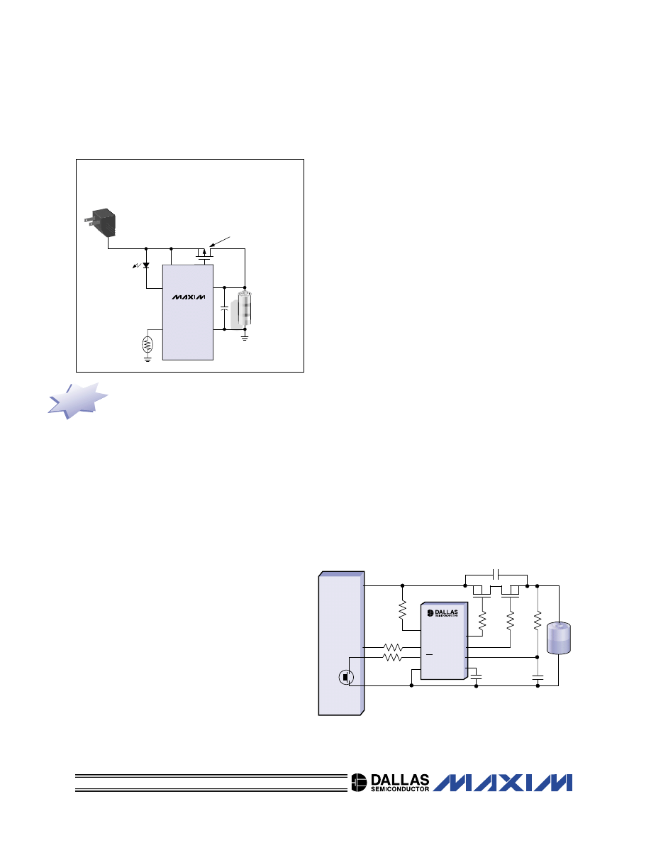
Cool Li+ Battery Charger Has
Virtually No Power Dissipation
Safe, Simple, and Inexpensive Pulse Charger Dissipates No Heat
Safety Features Include:
• Continuous Over/Undervoltage
Protection
• ±0.75% Charge Voltage Tolerance
• 6.25-Hour Charging Time-Out
Prevents Infinite Trickle-Charge
• Safely Precharges Near-Dead Cell
• Over/Undertemperature Protection
• Automatic Charging Restart at 4V
• Safe, Simple, and Inexpensive Pulse
Charger Dissipates No Heat
• Evaluation Kit Available to
Speed Designs
Single-Cell Li+ Protector Enables
Power Control Function in
Battery Pack
The DS2720* single-cell Li+ protection IC integrates memory, overtemperature protection, and the
ability to communicate with the host processor, along with the standard over/undervoltage and over-
charge protection found in popular standalone protectors. Because the host can communicate with the
DS2720, it can control the protection MOSFETs in software, enabling power control through the
DS2720 and MOSFET.
• Li+ Safety Circuit;
• Overvoltage Protection
• Overcurrent/Short-Circuit
Protection
• Undervoltage Protection
• Overtemperature Protection
• Controls High-Side N-Channel
Power MOSFETs
• System Power Management and
Control Feature Support
• 8 Bytes of Lockable EEPROM
• 1-Wire
®
, Multinode Digital
Communication Interface
• 8-Pin µSOP Package
+
-
PLS
CP
PS
DC
DQ
CC
V
SS
V
DD
DATA
PACK -
PACK +
POWER
SWITCH
HOST
DS2720
*Future product—contact factory for availability.
1-Wire is a registered trademark of Dallas Semiconductor.
FUTU
RE
PRO
DUC
T
PROTECTOR
(Lithium only)
64-BIT
ROM
TIME
TEMP
ADC
E
2
BATTERY PACK
V-
DATA
V+
HANDSET
BASEBAND
PROCESSOR/
ASIC
4.7k
Ω
Electronically Label Battery Packs
with Low-Cost, 1-Wire Digital
Interface ICs
• 1-Wire Digital Interface
• Unique 64-Bit Serial Number
• Reduces Battery Contacts
Reduced to Three, Regardless
of Device Chosen
• User-Programmable EEPROM:
16 Bits (DS1822), 256 Bits
(DS2436) 1024 Bits (DS2432)
• Real-Time Clock (DS2415)
• Local Temperature Sensor:
9 Bit to 12 Bit (DS1822),
13 Bit (DS2436)
• Battery-Voltage ADC:
10 Bit (DS2436)
• 512-Bit SHA-1 Encryption
Engine (DS2432)
Dallas Semiconductor silicon label ICs tag a unique and unchangeable electronic label to the battery
pack. Each offers an array of feature functions to fit different cellular phone applications. The low-cost
DS2401 is the base model of this series, containing a 64-bit ROM accessible from the 1-Wire serial digital
interface. The DS2415 adds a real-time clock to the serial number, eliminating the need to have a back-
up battery for the real-time clock in the host product. The DS1822 replaces thermistors in the battery
pack by integrating a local digital thermometer and 16 bits of EEPROM to the 64-bit ROM. The DS2432
features 1024 bits of user EEPROM and a 512-bit SHA-1 algorithm that encrypts the EEPROM array.
The security offered in the DS2432 deters non-OEM battery packs, thus enhancing accessory revenue
and more importantly, increasing the safety to the user of the product with lithium-based packs. The
DS2436 provides data storage in the form of the 64-bit ROM and 256-bit user EEPROM, and replaces the
pack thermistor and ADCs in the host reserved for measuring pack voltage.
Battery Pack ID Solutions Selector Table
TO-92, 8-SO,
Flip Chip (2.0 x 1.4)
6-TSOC,
Flip Chip (1.4 x 1.1)
Pin-Package
(mm
2
)
TO-92, 6-TSOC,
CSP (1.4 x 0.7)
6-TSOC,
Flip Chip (2.5 x 1.8)
DS1822
—
Part
64-Bit
ROM
Real-Time
Clock
1-Wire
Interface
DS2401
—
DS2415
DS2432
—
TO-92, 8-SO
DS2436
—
8-SO
DS2438
16-TSSOP,
Flip Chip (3.2 x 2.7)
DS2760
—
16-TSSOP
DS2770*
—
2
EEPROM
(Bytes)
—
—
1024 bits
32
40
32
32
12
Local Temp
Sensor (Bits)
—
—
—
13
13
11
11
—
Voltage
ADC (Bits)
—
—
—
10
10
11
11
—
Fuel
Gauge
—
—
—
—
—
Li+
Protector
—
—
—
—
—
Single
cell
—
DS1701K
EV Kit
—
—
—
DS2436K
DS2438K
DS2760K
DS2770K*
NEW
FUTU
RE
*Future product—contact factory for availability.
8-µSOP
DS2720*
—
8
—
—
—
Single
cell
DS2720K*
FUTU
RE
EN
SET
Li+
BATTERY
2.5V, 5.5V
OFF
ON
VCNTL
LED1
LED2
LED3
GND
SIMPLE
BRIGHTNESS
CONTROL
THIN SOT23
1mm HEIGHT
BETTER THAN
0.3% LED-TO-LED
MATCHING
5
10
15
20
25
30
3.0
3.2
3.4
3.6
3.8
4.0
4.2
BATTERY VOLTAGE (V)
LED CURRENT (mA)
350mV
3 RANDOM LEDs
USING MAX1916
SAME 3 LEDs USING
34.8
Ω BALLAST RESISTORS
POOR CURRENT
MATCHING
MAX1916
200mV
DROPOUT EXTENDS
BATTERY LIFE
BETTER MATCHING, LONGER BATTERY LIFE
+
ADDS 350mV
TO BATTERY LIFE
GOOD CURRENT
MATCHING
Power 3 White LEDs from Single Li+
with 0.3% Brightness Matching
Lowest Dropout (200mV) Current Regulator Fits in 1mm-Thin SOT23
The MAX1916 triple-output current regulator provides significantly better matching than tradi-
tional ballast resistor schemes and provides longer battery life. Ballast resistors only provide 2:1 LED
matching. The MAX1916 regulates three LED currents with 0.3% matching, eliminating costly factory
calibration and the need to purchase LEDs with matched forward voltages (VF). 200mV dropout allows
LEDs to be powered directly from a single-cell lithium-ion (Li+) battery for a longer time, extending
battery life.
The MAX1916 eliminates costly factory calibration and special batch ordering while improving battery life and brightness matching.
TRIPLE WHITE LED SUPPLY IS SUPERIOR TO BALLAST RESISTORS
High-Efficiency SOT23 Step-Up
Current Source Powers Up to 6 White
LEDs with Uniform Brightness
The MAX1848 is the
first high-efficiency step-up
DC-DC converter that
regulates current instead of
voltage to power white LEDs
for backlights in cell phones
and PDAs. It powers two or
three white LEDs in series
(up to 6 total), instead of in
parallel, to eliminate bright-
ness mismatch caused by
different threshold voltages.
An internal N-channel
MOSFET switch provides
85% efficiency, 40% better
than traditional doubling
charge-pump solutions.
MAX1848
V+
3.3
µF
33
µH
1
µF
CNTL
COMP
OUT
GND
CS
LX
LOGIC OR
DAC
OUTPUT
UP TO 13V
UP TO 60mA
INPUT
2.6V TO 5.5V
RSENSE
5
Ω
20
Ω
SERIES LEDs HAVE MATCHED LED
CURRENT AND UNIFORM BRIGHTNESS
NO CALIBRATION:
5% CURRENT TOLERANCE WITH
STANDARD LOW-COST
CHIP RESISTOR
PROGRAMMABLE
BRIGHTNESS
MATCHED CURRENT
=
UNIFORM BRIGHTNESS
2
.8
m
m x 2.9
m
m
8-
PIN
SOT2
3
0.15
µF
3.0
4.0
4.5
INPUT VOLTAGE (V)
90
85
80
75
70
65
60
55
50
45
40
35
30
EFFICIENCY (%)
3.5
40% MORE EFFICIENT,
1.8x LONGER BATTERY LIFE
I
OUT
= 15mA
1.8x
LONGER
BATTERY
LIFE
DOUBLING CHARGE
PUMP WITH THREE
LEDs IN PARALLEL
LOWER INPUT RIPPLE
THAN CHARGE PUMP
NEW
MAX1848
WITH THREE LEDs
IN SERIES
25
Ω
NO BALLAST RESISTORS AND
NO FACTORY CALIBRATION
Most Efficient 1.4MHz SOT23
Current-Mode Step-Up DC-DC
Converter
0.7
Ω On-Resistance and 200µA I
Q
—Highest Efficiency
MAX1896
SS
INPUT
2.6V to 5.5V
GND
R2
R1
100
90
80
EFFICIENCY (%)
70
60
50
0
100
200
OUTPUT CURRENT (mA)
BETTER EFFICIENCY
300
400
ON
OPTIONAL
SOFT-START
OFF
FB
LX
1
3
2
4
6
5
SHDN
IN
OUTPUT
UP TO 13V,
UP TO 600mA
MAX1896
V
IN
= 3.3V
V
OUT
= 5V
COMPETITION
The MAX1896 is pin compatible with the LT1613 and has higher efficiency due to lower switch on-resistance and lower quiescent
supply current.
3
.0
m
m x 3.0
m
m
6-
PIN
SOT2
3
MOST EFFICIENT & SMALLEST SOT23 13V STEP-UP CONVERTER
The MAX1896 uses current-mode control and 1.4MHz fixed-frequency pulse-width modulation
(PWM) to provide over 90% efficiency, fast transient response, and operation with physically smaller
components. It features 200µA quiescent supply current, low R
ON
(on-resistance), 0.01µA logic-
controlled shutdown current, and programmable soft-start. The MAX1896 is intended for PDAs, LCD
panels, and hand-held equipment.
Battery and load
disconnect
Battery connects
to load
Battery connects
to load
IN SHUTDOWN
MAX1834
OUTPUT
Adjustable (2V to 5.5V)
Fixed 3.3V
Adjustable (2V to 5.5V)
MAX1833
MAX1832
PART
NUMBER
Battery and load
disconnect
MAX1835
Fixed 3.3V
World’s First Step-Up Converters
with “Reverse-Battery” Protection
SOT23 Boost Converters Use Only 4µA and Integrate Protection to
Save Cost
MAX1832
MAX1833
MAX1834
MAX1835
GND
P
N
INTERNAL SWITCH
OPENS IF BATTERY
IS REVERSED
PROTECTION INTEGRATED; SYNCHRONOUS RECTIFIER INTEGRATED
OUTPUT
2V TO 5.5V
UP TO 150mA
TINY
6-PIN SOT23
SAVES SPACE
INPUT
RANGE
1.5V TO 5.5V
BATTERY
ACCIDENTLY
REVERSED
-
+
SHDN
OFF
ON
NO REVERSE CURRENT
(IN-FAULT CONDITION)
FAULT
CONDITION
Wyszukiwarka
Podobne podstrony:
SWITCHING POWER SUPPLY DESIGN CONTINUOUS MODE FLYBACK CONVERTER
atx Power Supply Design Guide
DESIGN OF A SWITCHING MODE POWER SUPPLY WITH UPS FEATURES
Convert Computer ATX Power Supply to Lab Power Supply
Jvc Power Supply Description And Trouble Shooting Procedure
Battery Inverter For Modularly Structured Pv Power Supply Systems
0 50V 2A LM10C, 0 50V 2A Bench power supply circuit diagrams, schematics, electronic projects
(Wydruk – ATX Switching Power Supply 13,8 V Proste zmiany w celu zwiększenia napięcia wyjściowego Ja
Alarm Power Supply L78Sxx id 61 Nieznany (2)
3 2 Lab Install Power Supply
HY3010 power supply, Elektronika, Zasilacze, Zasilacz HY3010, Zasilacz HY3010, HY3010 ,INSTRUKCJA
Lekturki Power Supply Unit Lekturka
How to Modify an ATX Computer Power Supply
Adaptive fuzzy control for uninterruptible power supply with three phase PWM inverter
Control and Power Supply for Resistance Spot Welding (RSW)
Performance Improvements in an arc welding power supply based on resonant inverters (1)
Convert Computer ATX Power Supply to Lab Power Supply
(ebook free energy) 50000 vdc power supply
(ebook electronics) Schematics Power Regulated Power Supply for CB & Ham Radio
więcej podobnych podstron