GSM TELEPHONE
SGH-E810
GSM TELEPHONE
CONTENTS
1.
Specification
2.
Flow Chart of Troubleshooting
3.
Exploded Views and Parts List
4.
Electrical Parts List
5.
Block Diagrams
6.
PCB Diagrams
SERVICE
Manual
SAMSUNG Proprietary-Contents may change without notice
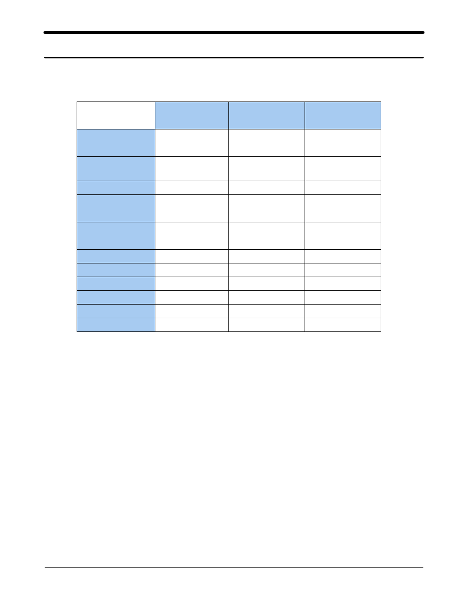
1. SGH-E810 Specification
This Document can not be used without Samsung's authorization
1-1
GSM900
Phase 1
EGSM900
Phase 2
DCS1800
Phase 1
Freq. Band[MHz]
Uplink/Downlink
890~915
935~960
880~915
925~960
1710~1785
1805~1880
ARFCN Range
1~124
0~124 &
975~1023
512~885
Tx/Rx Spacing
45MHz
45MHz
95MHz
Mod. Bit Rate/
Bit Period
270.833KHz
3.692us
270.833KHz
3.692us
270.833KHz
3.692us
Time Slot Period
/Frame Period
576.9us
4.615ms
576.9us
4.615ms
576.9us
4.615ms
Modulation
0.3GMSK
0.3GMSK
0.3GMSK
MS Power
33dBm~13dBm
33dBm~13dBm
33dBm~13dBm
Power Class
5pcl~15pcl
5pcl~19pcl
0pcl~15pcl
Sensitivity
-102dBm
-102dBm
-100dBm
TDMA Mux
8
8
8
Cell Ridius
35Km
35Km
2Km
1. GSM General Specification
SAMSUNG Proprietary-Contents may change without notice
SGH-E810 Specification
1-2
This Document can not be used without Samsung's authorization
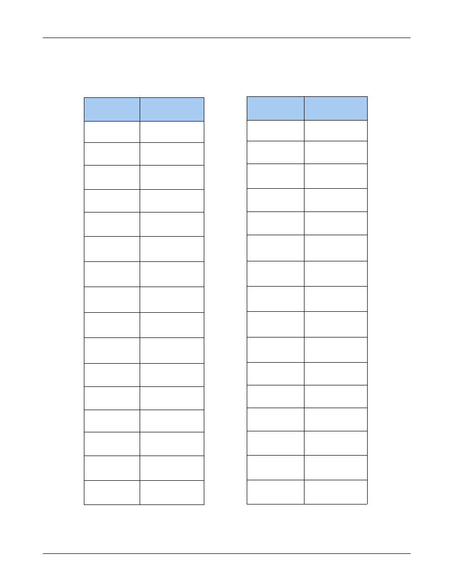
2. GSM TX power class
TX Power
Control Level
GSM900
5
33±2dBm
6
29±2dBm
7
27±2dBm
8
25±2dBm
9
23±2dBm
10
21±2dBm
11
19±2dBm
12
17±2dBm
13
15±2dBm
14
13±2dBm
15
11±2dBm
16
9±3dBm
17
7±3dBm
18
5±3dBm
19
3±3dBm
TX Power
Control Level
DCS1800
0
30±3dBm
1
28±3dBm
2
26±3dBm
3
24±3dBm
4
22±3dBm
5
20±3dBm
6
18±3dBm
7
16±3dBm
8
14±3dBm
9
12±4dBm
10
10±4dBm
11
8±4dBm
12
6±4dBm
13
4±4dBm
14
2±5dBm
15
0±5dBm
SAMSUNG Proprietary-Contents may change without notice
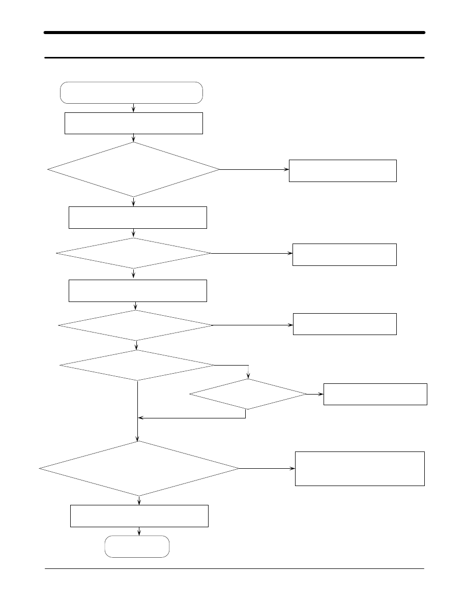
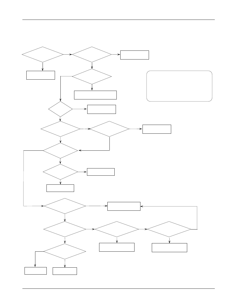
2. SGH-E810 Flow Chart of Troubleshooting
2-1
This Document can not be used without Samsung's authorization
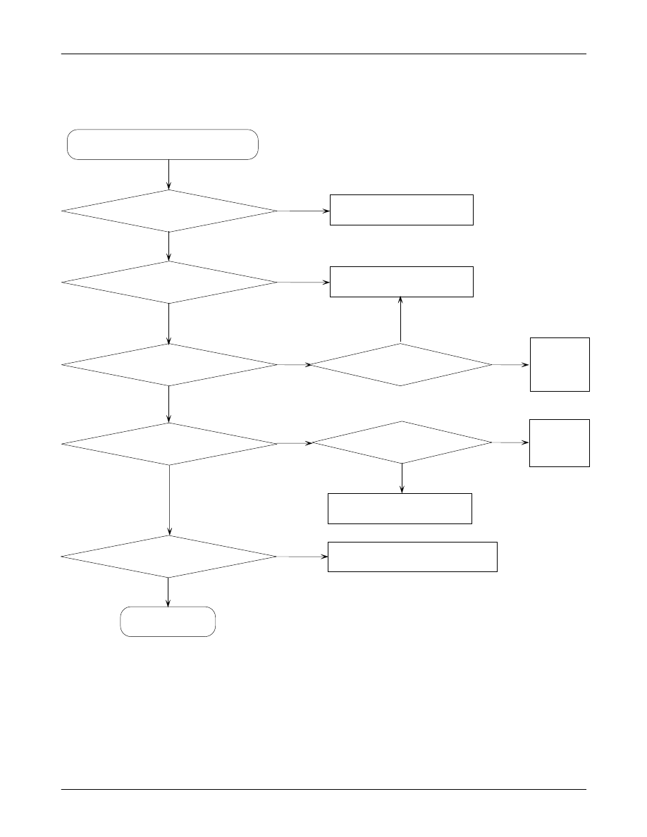
1. Power ON
'Power ON' Does not work
Check the current consumption
Current consumption
≥100mA ?
Check the V bat. voltage
Down load again
Voltage ≥ 3.3V ?
Check the pin of U100
pin #11 ≥ 2.8V ?
Pin #9=1.8V?
Check the Initial operation
END
pin #39 and #33 = 2.8V
Charge the Battery
Check the clock generation
circuit (OSC400, U405 pin#4)
Check the clock signal
at pin #3 of OSC400
Freq.=13MHz,Vrms 300mV
Check U100 and C113
Check U100 and C114
NO
NO
NO
NO
NO
NO
YES
YES
YES
YES
YES
YES
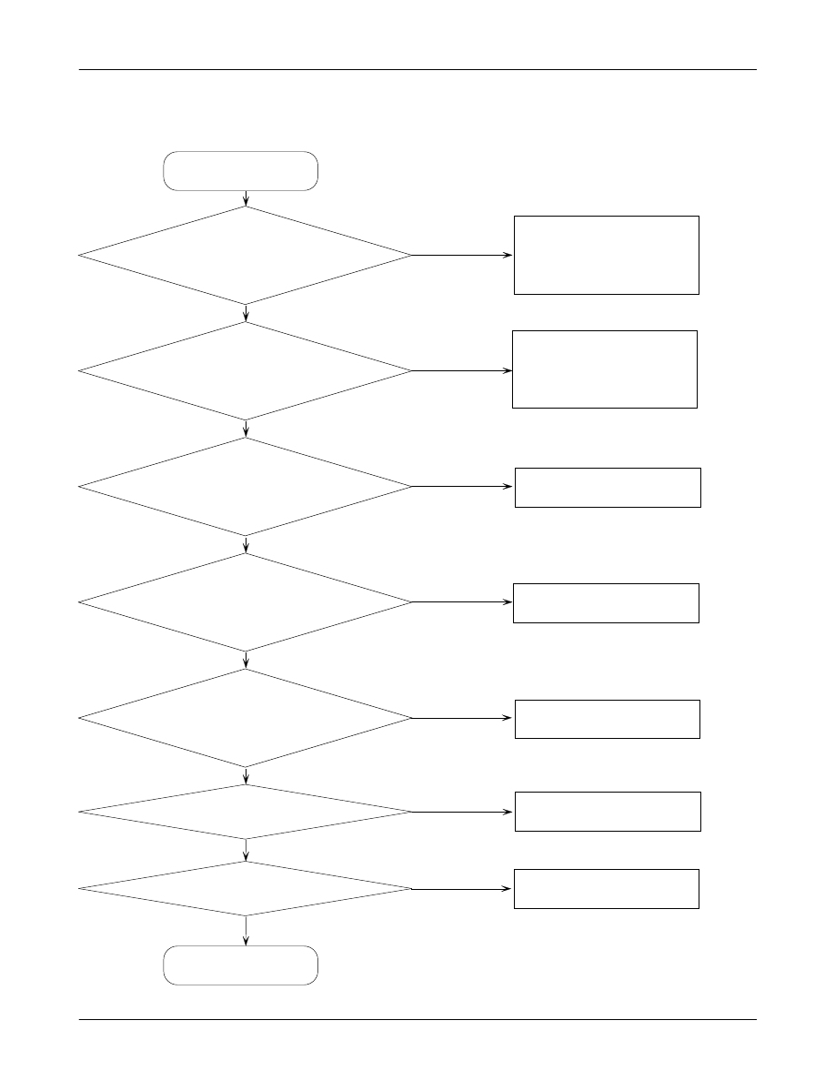
SAMSUNG Proprietary-Contents may change without notice
SGH-E810 Flow Chart of Troubleshooting
2-2
This Document can not be used without Samsung's authorization
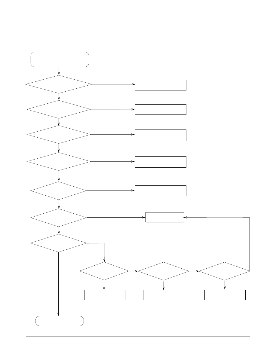
2. System Initial
The pin #9 of U100 = 1.8V
and pin #11 of U100=2.8V?
Initial Failure
Is the pin #19 of U100
" Low --> High" ?
There is 32.768KHz wave
form at the C327, C328 ?
Is the pin #25 of U100
is High ?
The voltage is "High"
at the C107,C109,C110 ?
LCD Display OK ?
Sound operation OK ?
END
Check the U304
Check the U300
Check the U100
Check the LCD part
Check the Audio part
YES
NO
NO
NO
NO
YES
YES
YES
YES
YES
NO
NO
NO
YES
Check the U100
(If it has some problem,
it has to be replaced.)
Check the U100
(If it has some problem,
it has to be replaced.)
SAMSUNG Proprietary-Contents may change without notice
SGH-E810 Flow Chart of Troubleshooting
2-3
This Document can not be used without Samsung's authorization
3. SIM Part
Is there any signal
pin #52,53,54 of U100 ?
Check the U304
"Insert SIM" is displayed on the LCD
END
Check the SIM Card
YES
NO
NO
YES
Is there any signal
pin #1,2,3,6 of CN100 ?
Check the U100
SAMSUNG Proprietary-Contents may change without notice
SGH-E810 Flow Chart of Troubleshooting
2-4
This Document can not be used without Samsung's authorization
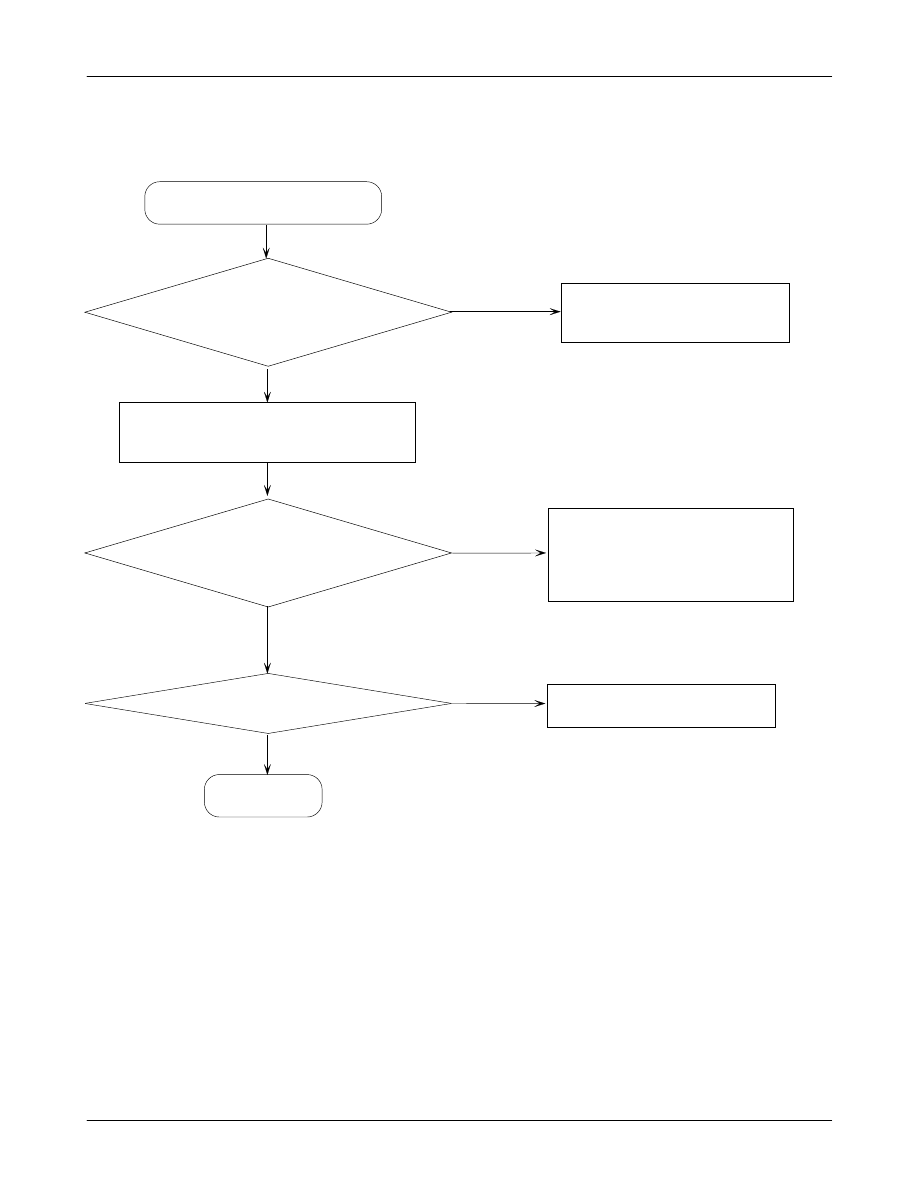
4. Microphone Part
Micro-phone does not work
Is the assembled status of
Microphone O.K?
YES
Reassemble the microphone
NO
Check the DC bias voltage on
Mic path.
The voltage of C246 is
2.2V±10%?
NO
Solder the microphone again
or Replace
C233,C246,R232,R233,R235
Is microphone OK?
NO
Check U300
END
YES
YES
SAMSUNG Proprietary-Contents may change without notice
SGH-E810 Flow Chart of Troubleshooting
2-5
This Document can not be used without Samsung's authorization
5. Speaker Part
Is the terminal of speaker
is O.K?
NO
Replace the speaker
Are there any signal
at the pin #1,3 of CN503?
NO
Check the SPK module
& Replace CN503
There is no sound from speaker
YES
YES
The type of sound from
the speaker is Melody?
YES
NO
Are there any signal
at the pin #5,7 of U201?
Are there any signal
at the pin #3,9 of U201?
Check
U201,
U304
NO
NO
Pin #4 of U201
is Low?
Pin #4 of U201
is High?
Check U200
Check U300
NO
NO
YES
YES
YES
YES
END
SAMSUNG Proprietary-Contents may change without notice
SGH-E810 Flow Chart of Troubleshooting
2-6
This Document can not be used without Samsung's authorization
J
A
C
K
_
IN
E
A
R
_
S
P
K
_
P
A
U
D
IO
E
A
R
_
S
P
K
_
N
E
A
R
_
M
IC
_
P
E
A
R
_
M
IC
_
N
4
.7
K
R
2
3
7
C
2
4
0
4
7
P
F
Z
D
2
0
1
C
2
5
0
3
3
U
F
6
.3
V
3
9
P
F
R
2
3
6
1
0
0
K
C
2
5
4
3
3
P
F
C
2
6
1
C
2
3
6
1
N
F
R
2
4
1
1
K
C
2
6
2
39
PF
C
26
3
3
9
P
F
39
PF
C2
64
V
C
C
A
L
2
0
0
1
0
0
n
H
U
2
0
2
IC
E
B
E
R
G
-F
P
C
B
1
U
F
C
2
3
3
8
2
P
F
Z
D
2
0
2
R
2
4
0
8
2
K
,1
%
C
2
5
1
C
2
5
5
1
8
0
P
F
3
3
U
F
C
2
4
6
4
7
P
F
2
.7
K
R
2
3
1
C
2
4
2
L
2
0
3
1
0
0
n
H
L
2
0
2
1
0
0
n
H
R
2
2
8
V
C
C
A
6
8
0
C
2
5
8
1
N
F
3
3
U
F
C
2
4
8
4
7
0
n
F
C
2
3
2
6
.3
V
1
0
0
n
H
L
2
0
4
V
C
C
A
V
C
C
A
Z
D
2
0
0
R
2
3
9
6
8
K
V
C
C
D
Z
D
2
0
3
1
2
3
4
L
2
0
1
0
R
2
4
2
3
9
P
F
Z
D
2
0
4
C
2
6
0
3
3
P
F
N
C
C
2
4
4
4
7
0
n
F
4
5
6
7
C
2
2
8
C
N
2
0
1
2
3
C
2
5
9
1
N
F
C
2
5
7
1
N
F
C
2
5
2
C2
34
NC
R
2
3
2
1
0
K
1
U
F
C
2
4
9
C
2
5
3
3
9
P
F
C
2
4
1
5
.6
P
F
C
2
5
6
3
3
U
F
6
.3
V
5
1
K
R
2
3
3
5
6
K
,1
%
R
2
4
4
R
2
3
8
1
0
K
R
2
3
5
6
8
0
Q
2
0
0
2
3
1
1
K
R
2
4
3
M
IC
+
J
A
C
K
_
IN
E
A
R
_
S
W
IT
C
H
M
IC
IN
M
IC
O
U
T
A
U
X
IN
A
U
X
O
U
T
A
O
U
T
B
P
A
O
U
T
B
N
SAMSUNG Proprietary-Contents may change without notice
SGH-E810 Flow Chart of Troubleshooting
2-7
This Document can not be used without Samsung's authorization
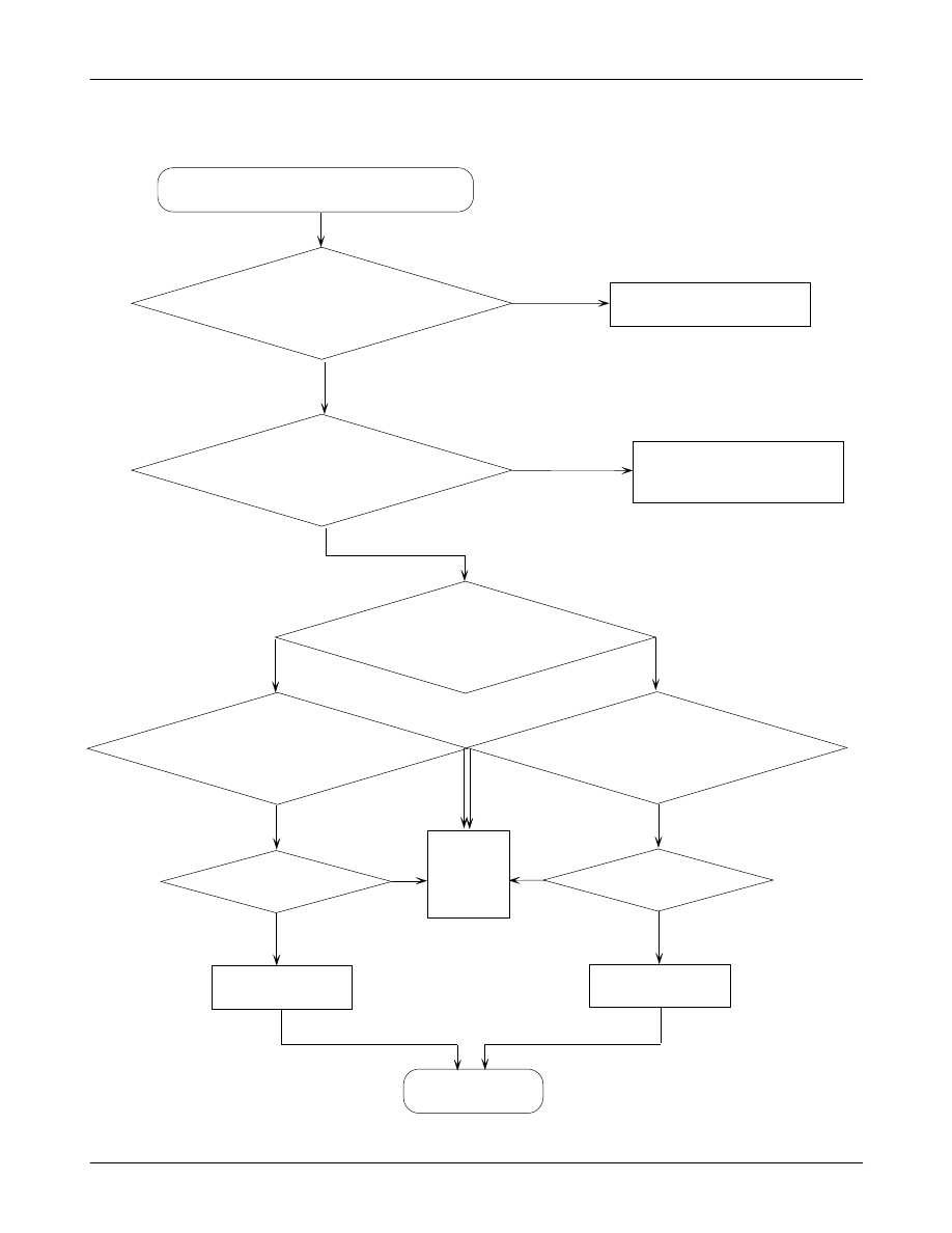
6. Camera Part
Camera function does not work
Check the connect CN502?
NO
Connect the CN502
Pin #9 of U500 = 2.8V?
NO
NO
Pin#3 of OSC500 is 25MHz?
NO
Pin #10 of U500 = 2.8V?
Check
U503
END
YES
YES
YES
YES
Pin#1 of OSC500 = High?
NO
Pin #2 of U500 = High?
YES
Check the U500
Check
U304
NO
NO
Pin#1 of CN502 is High?
Check solder status of
R500, C502
Replace the OSC500
YES

SAMSUNG Proprietary-Contents may change without notice
SGH-E810 Flow Chart of Troubleshooting
2-8
This Document can not be used without Samsung's authorization
7. EGSM Receiver
Continuous RX ON
RF Input : 62 CH
AMP : -50dBm
NORMAL CONDITION
Catch the channel ?
YES
NO
U401 Check
Pin #8 ≥ -65dBm ?
U401 Check
Pin #10 ≥ -65dBm ?
U404 Check
Pin#20,21 ≥ -65dBm ?
Check soldered status of
R400, C401
CN400
Resolder or Change
U401 Resolder or Change
U404 Check
Pin#9,32=Clean 2.8V?
U404 Check
Pin#28,1,2,3=100mV?
U100,C107,C109
Check or resolder
Check U300
NO
NO
YES
YES
YES
YES
NO
YES
U404 Check
Pin #8 : 13MHz ?
Vpp : 860mV?
OSC400 Check
Pin #3 : 13MHz ?
Vpp : 950mV?
OSC400 Check
Pin #4 = 2.8V ?
U404
Change or resolder
NO
NO
NO
R413,C428
resolder
OSC400
Change or resolder
YES
YES
YES
NO
Check soldered status of
C417,419,L405,U403
U403 Check
Pin #1 ≥ -65dBm ?
Check soldered status of
C418 &
U401 Resolder or Change
NO
YES
NO
SAMSUNG Proprietary-Contents may change without notice
SGH-E810 Flow Chart of Troubleshooting
2-9
This Document can not be used without Samsung's authorization
8. EGSM Transmitter
Continuous TX ON condition
TX Power Code : 500 code Applied
CH : 62
RBW : 100KHz
VBW : 100KHz
SPAN : 10MHz
REF. Level : 10dBm
ATT. : 20dB
C402
= 3.7V?
Change U400
NO
YES
U401 Pin#8
About 2~3 dBm?
U401
Pin#11 = High?
U300,301
Check & Change
NO
C401,CN400
Check & Change
YES
U401
Check & Change
YES
Check the
Battery Block
Level of
U400 Pin #6 is
1.2V?
Check
& Change R401
OK ?
U300
Check & Change
YES
YES
NO
NO
NO
NO
U400 pin#7
About -5 dBm?
U400 pin#3
High ?
Check U300
YES
NO
YES
U404 Check
Pin#9,32 ≥ 2.8V ?
U404 Check
Pin #8 : 13MHz ?
Vpp : 860mV?
OSC400 Check
Pin #3 : 13MHz ?
Vpp : 950mV?
OSC400 Check
Pin #4 = 2.8V ?
NO
YES
NO
NO
NO
R413,C428
resolder
OSC400
Change or resolder
YES
YES
YES
NO
U100,C107,C109
Check or resolder
U404 Pin
#4,5,6,7 = 1.7V?
YES
Change U400
Check U300
NO
YES
Level of
U401 Pin#5 is
4~5dBm ?
SAMSUNG Proprietary-Contents may change without notice
SGH-E810 Flow Chart of Troubleshooting
2-10
This Document can not be used without Samsung's authorization
9. DCS Receiver
Continuous RX ON
RF Input : 660 CH
AMP : -50dBm
NORMAL CONDITION
Catch the channel ?
YES
NO
U401 Check
Pin #8 ≥ -65dBm ?
U401 Check
Pin #1 ≥ -65dBm ?
U404 Check
Pin#18,19 ≥ -65dBm ?
Check soldered status of
R400, C401
CN400
Resolder or Change
U401 Resolder or Change
U404 Check
Pin#9,32=Clean 2.8V?
U404 Check
Pin#28,1,2,3=100mV?
U100,C107,C109
Check or resolder
Check U300
NO
NO
YES
YES
YES
YES
NO
YES
U404 Check
Pin #8 : 13MHz ?
Vpp : 860mV?
OSC400 Check
Pin #8 : 13MHz ?
Vpp : 950mV?
OSC400 Check
Pin #4 = 2.8V ?
U404
Change or resolder
NO
NO
NO
R412,C426
resolder
OSC400
Change or resolder
YES
YES
YES
NO
Check soldered status of
C414, 416, L404, U402
U402 Check
Pin #1 ≥ -65dBm ?
Check soldered status of
C415
NO
YES
NO
SAMSUNG Proprietary-Contents may change without notice
SGH-E810 Flow Chart of Troubleshooting
2-11
This Document can not be used without Samsung's authorization
10. DCS Transmitter
Continuous TX ON condition
TX Power Code : 350 code Applied
CH : 660
RBW : 100KHz
VBW : 100KHz
SPAN : 10MHz
REF. Level : 10dBm
ATT. : 20dB
C402
= 3.7V?
Change U400
NO
YES
U401 Pin#8
About 2~3 dBm?
U401
Pin#11 = High?
U300,302
Check & Change
NO
C401,CN400
Check & Change
Level of
U401 Pin#3 is
4~5dBm ?
YES
U401,L402,C405,407,408
Check & Change
YES
Check the
Battery Block
Level of
U400 Pin #6 is
1.2V?
Check
& Change R401
OK ?
U300
Check & Change
YES
YES
NO
NO
NO
NO
U400 pin#1
About -5 dBm?
U400 pin#3
High ?
Check U300
YES
NO
YES
U404 Check
Pin#9,32 ≥ 2.8V ?
U404 Check
Pin #8 : 13MHz ?
Vpp : 860mV?
OSC400 Check
Pin #3 : 13MHz ?
Vpp : 950mV?
OSC400 Check
Pin #4 = 2.8V ?
NO
YES
NO
NO
NO
R413,C428
resolder
OSC400
Change or resolder
YES
YES
YES
NO
U100,C107,C109
Check or resolder
U404 Pin
#4,5,6,7 = 1.7V?
YES
Change U400
Check U300
NO
YES
SAMSUNG Proprietary-Contents may change without notice
SGH-E810 Flow Chart of Troubleshooting
2-12
This Document can not be used without Samsung's authorization
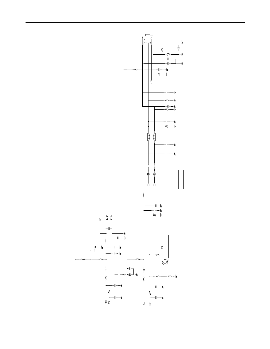
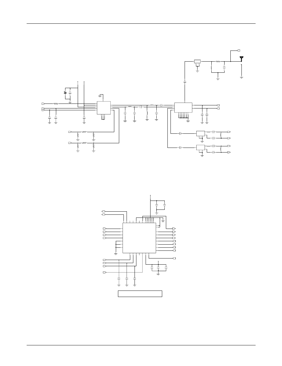
TRANSMITTER & RECEIVER
C404
47PF
0.75PF
C417
33PF
C433
C408
0.5PF
R406
220
C403
10NF
33PF
C430
2.2PF
C414
100K
L401
6.8nH
R401
R402
10
33PF
C435
820
R403
2.2PF
C416
15
VRF
47PF
C418
R405
2.7nH
L402
NC
L403
OUT
3
4
OUT
VPAC
VRF
U402
G
2
G
5
1
IN
NC
VBAT
C400
L404
C406
2.2PF
6.8nH
27nH
L405
C434
33PF
C419
0.75PF
1UF
C429
OUT
CN400
G1
3
G2
4
1
IN
2
2
L407
15nH
G
G
6
7
G
G
9
12
G
G
13
14
G
11
VC1
VC2
U401
8
ANT
1
DCS_RX
3
DCS_TX
EGSM_RX
10
EGSM_TX
5
4
R407
270
100NF
C420
22PF
C405
C411
270PF
ANT_GND
C407
0.75PF
25
G
1
IN
OUT
3
4
OUT
U403
G
820
R404
6.3V
100UF
C402
R400
0
27
X
O
U
T
_
P
D
N
10
12
_
S
E
N
5
TXIN
TXIP
4
7
TXQN
TXQP
6
V
D
D
9
32
V
D
D
26
X
E
N
8
X
IN
R
F
O
G
23
3
RXIN
RXIP
2
RXQN
1
R
X
Q
P
28
13
S
C
L
K
S
D
I
14
11
S
D
O
GND
19
RFIDN
18
RFIDP
21
RFIGN
RFIGP
20
17
RFIPN
RFIPP
16
22
R
F
O
D
D
IA
G
2
15
GND
29
G
N
D
30
G
N
D
G
N
D
31
33
G
N
D
34
G
N
D
GND
35
36
U404
24
D
IA
G
1
25
C412
33PF
6
5
VREG
1NF
C413
7
GSM850/900IN
9
GSM850/900OUT
PCSOUT
11
TXEN
3
VBATT
4
V
C
C
10 8
V
C
C
2
V
C
C
2
12
VRAMP
U400
RF3140
BAND
21
DCSIN
GND
13
C410
33PF
33PF
C409
ANT1
C431
22NF
C401
47PF
22PF
C415
C421
33PF
ANT
SERLE
SERCLK
SERDAT
GSM_LNA_IN_P
GSM_LNA_IN_N
DCS_LNA_IN_P
DCS_LNA_IN_N
TX_BAND_SEL
DCS_TX_EN
GSM_TX_EN
DCS_LNA_IN_P
DCS_LNA_IN_N
GSM_LNA_IN_N
GSM_LNA_IN_P
SI_EN
RXQP
GSM_PAM_IN
DCS_PAM_IN
CLK13M_R
TXIN
TXIP
TXQN
TXQP
TXPOWER
GSM_PAM_IN
DCS_PAM_IN
TX_EN
RXIP
RXIN
RXQN
SAM SU N G Proprietary-C ontents m ay change w ithout notice
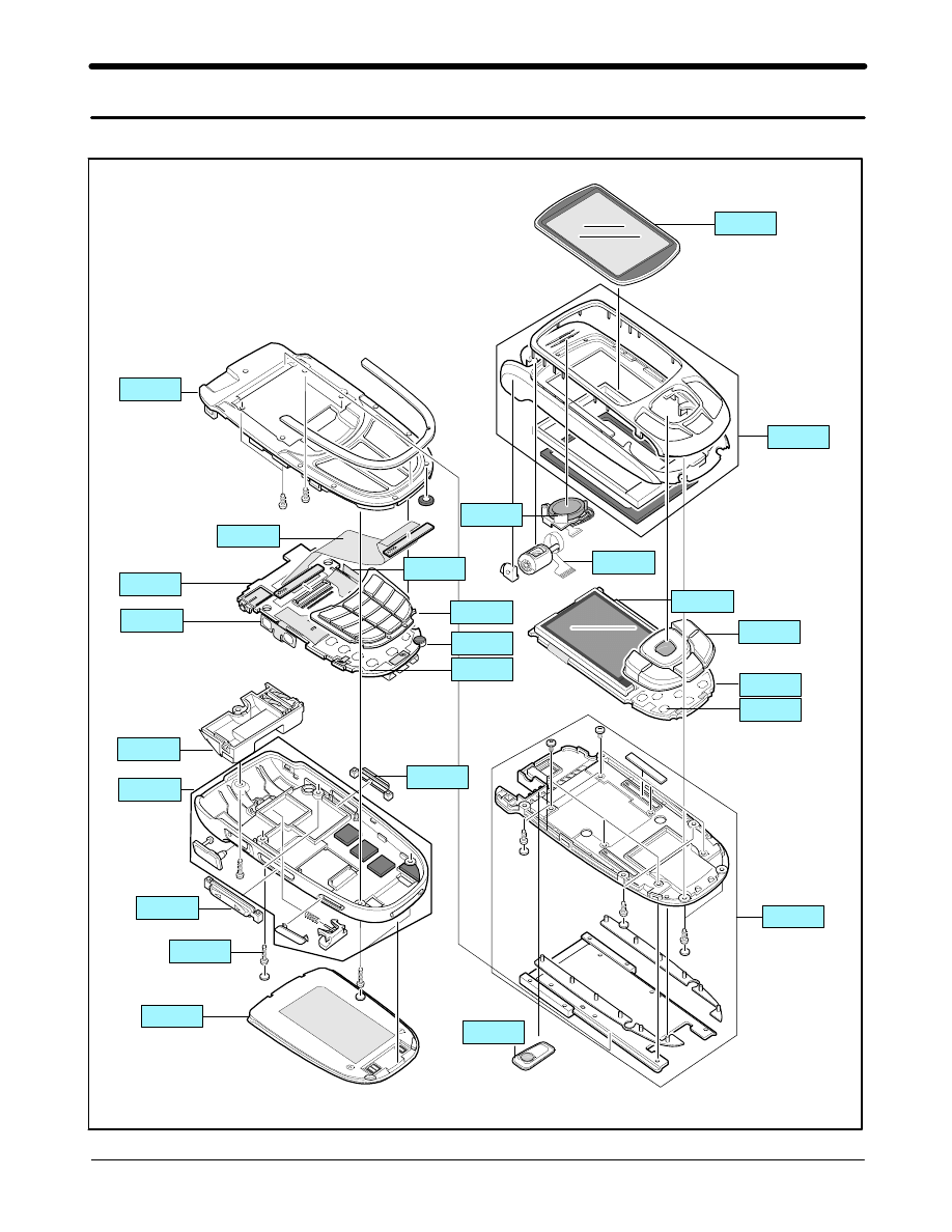
3. SGH-E810 Exploded View and Parts list
3-1
This Document can not be used without Samsung's authorization
1. Cellular phone Exploded View
Q M W 02
Q FU 01
Q KP02
Q M P02
Q FL01
Q C A01
Q VK02
Q M E02
Q LC 55
Q FR 01
Q M P01
Q VK01
Q M I01
Q KP01
Q M E01
Q R E01
Q AN 02
Q VO 01
Q C R 03
Q C K01
Q BA29
Q C H 05
Q C A02
Q M E03
SAM SU N G Proprietary-C ontents m ay change w ithout notice
SGH- E810 Exploded View and Part list
3-2
This Document can not be used without Samsung's authorization
Location NO.
Description
SEC CODE
Remark
QMW02
MAIN WINDOW
GH72-14922A
QFU01
FOLDER UPPER
GH75-04239A
QVK02
UNIT FLASH FPCB
GH59-01353A
QCA01
CAMERA
GH59-01328A
QLC55
LCD
GH07-00535A
QKP02
FUNCTION KEY
GH75-04245A
QMP02
MAIN PBA
GH92-01750A
QME02
METAL DOME
GH59-01336A
QME03
UNIT-FPCB
GH59-01408A
QFL01
FOLDER LOWER
GH75-04743A
QCH05
FRESH COVER
GH72-12929A
QFR01
FRONT COVER
GH75-04238A
QCA02
CAMERA KEY
GH59-01338A
QKP01
KEYPAD
GH75-04244A
QMI01
MIC
GH30-00107A
QME01
METAL DOME
GH59-01335A
QMP01
MAIN PBA
GH92-01747A
QVK01
UNIT VOLUME
GH59-01337A
QAN02
INTENNA
GH42-00415A
QRE01
REAR COVER
GH75-04246A
QCK01
CAMERA KEY
GH75-04247A
QVO01
VOLUME KEY
GH75-04248A
QCR03
SCREW
6001-001811
QBA29
BATTERY
GH43-01319A
2. Cellular phone Parts list
SAM SU N G Proprietary-C ontents m ay change w ithout notice
SGH-E810 Exploded View and Part list
3-3
This Document can not be used without Samsung's authorization
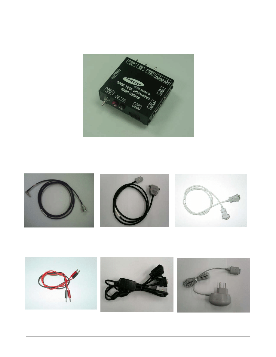
3. Test Jig (G H 80-03304A)
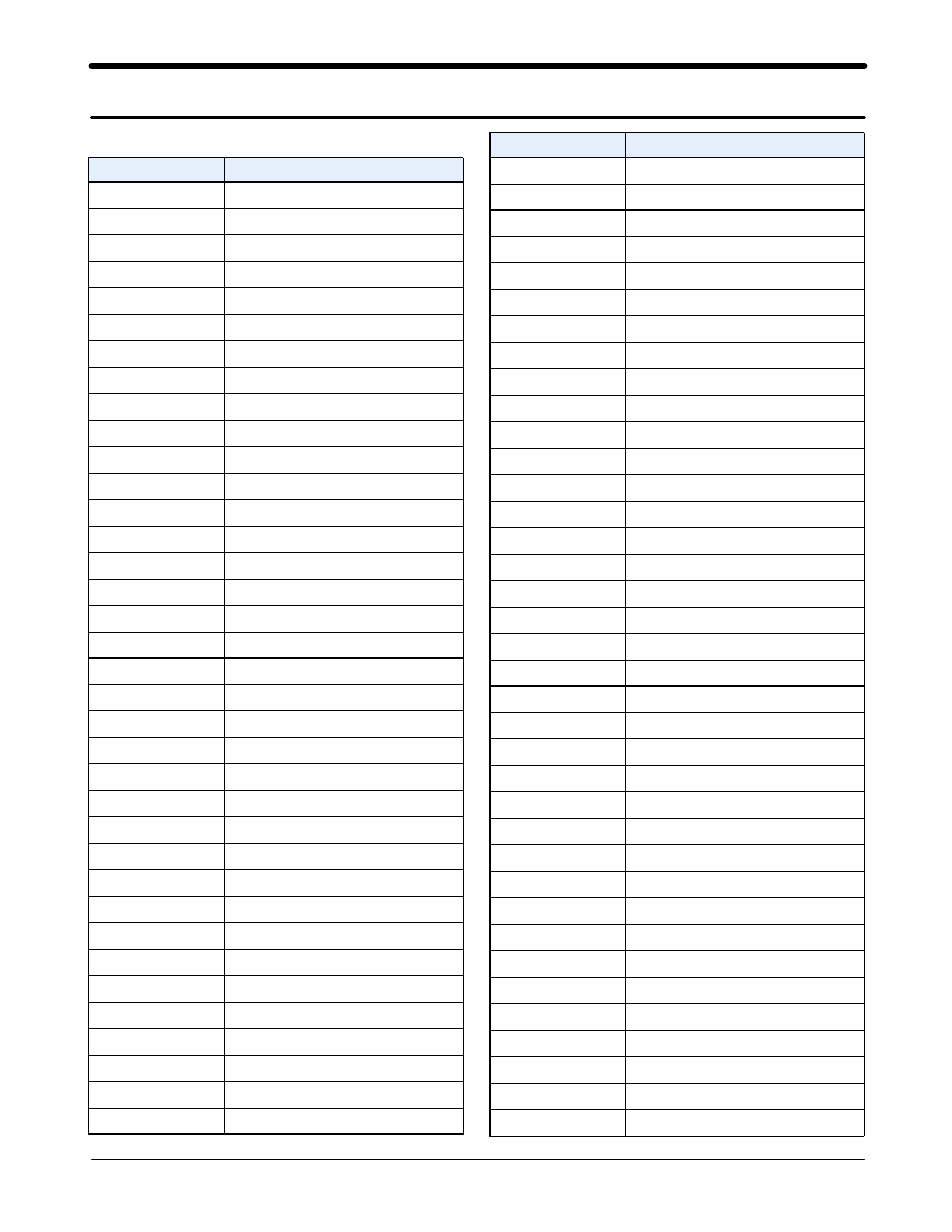
3-1. RF Test Cable
(GH39-00182A)
3-2. Test Cable
[GH39-00304A]
3-3. Serial Cable
3-4. Power Supply Cable
3-5. DATA CABLE
[GH39-00293A]
3-6. TC
[GH44-00701A]
SAMSUNG Proprietary-Contents may change without notice
4. SGH-E810 Electrical Parts List
4-1
This Document can not be used without Samsung's authorization
1.Main Parts List
SEC Code
Design LOC
4302-001130
BAT1
2203-006257
C100,C119,C228,C248
2203-000812
C101,C102,C103,C260
2203-005061
C104,C105,C225,C227
2203-000233
C106,C116,C235,C239
2203-006201
C107,C108,C109,C113
2404-001268
C110
2404-001305
C111
2203-001652
C112
2203-006201
C114,C115,C237
2203-006208
C117
2404-001225
C118
2203-006093
C200,C201,C233,C249
2203-000643
C202,C203,C204,C205
2203-000643
C206,C207,C208,C209
2203-000643
C210,C211,C212,C213
2203-000643
C214,C215,C216,C217
2203-000643
C218,C219,C220,C221
2203-000643
C222
2203-000654
C223,C411
2404-001086
C224,C229
2203-001405
C226,C301
2203-005061
C230,C300,C310,C317
2203-000438
C231,C236,C252,C257
2404-001151
C232,C246,C250,C256
2203-000995
C240,C242,C324,C401
2203-005055
C241
2203-000585
C243,R234
2007-000171
C245,R242,R245,R316
2203-001239
C251
2203-000854
C253,C254,C262,C263
2203-005503
C255
2203-000438
C258,C413,C423,C424
1405-001082
C259,V1,V10,V11,V12
2203-000812
C261,C409,C410,C412
2203-000854
C264,ZD204
SEC Code
Design LOC
2203-000254
C302,C303,C306,C315
2203-005496
C304,C314,C334
2203-000679
C305,C308,C309
2203-000233
C307,C311,C318,C325
2203-006093
C312,C429
2203-005450
C313
2203-000254
C316,C319,C320,C321
2203-000254
C322,C330,C332,C336
2203-005052
C323
2203-005482
C326
2203-000330
C327,C328
2203-000233
C329,C425,C426
2203-005061
C331,C333,C420
2203-000940
C335
2404-001134
C402
2203-000254
C403,C422,C427,C428
2203-000995
C404,C418
2203-000628
C405,C415
2203-005552
C406,C414,C416
2203-002677
C407,C417,C419
2203-002668
C408
2203-000812
C421,C430,C433,C434
2203-006137
C431
2203-000254
C432
2203-000812
C435
3709-001187
CN100
3710-002128
CN101
3708-001853
CN200
3722-002186
CN201
3705-001287
CN400
0409-001044
D300
2901-001296
F1,F2,F3,F4,F5,F6
2703-002313
L200,L202,L203,L204
2901-001271
L201
3301-001342
L300
2703-002170
L401
2703-001737
L402
SAMSUNG Proprietary-Contents may change without notice
4-2
SGH-E810 Electrical Parts List
This Document can not be used without Samsung's authorization
SEC Code
Design LOC
2703-002547
L404
2703-001907
L405
3301-001105
L406
2703-001180
L407
0601-001790
LED100,LED101,LED102
0601-001790
LED103,LED104,LED105
2801-003747
OSC300
2809-001264
OSC400
0504-001141
Q100
0501-000225
Q200
0504-001140
Q300
2007-000157
R100,R101,R102,R103
2007-000143
R104,R237
2007-000140
R105,R106,R107,R108
2007-000140
R109,R110,R111,R112
2007-000140
R113,R114,R115,R116
2007-000758
R117
2007-001319
R118
2007-000174
R119,R120,R121,R122
2007-000174
R123,R126,R127,R128
2007-007009
R124,R125
2007-001301
R129,R130,R131,R132
2007-001301
R133,R134
2007-000174
R200,R202,R203,R204
2007-000140
R201,R241,R243,R310
2007-000174
R205,R206,R207,R208
2007-000174
R209,R210,R211,R212
2007-000174
R213,R214,R215,R216
2007-000174
R217,R218,R219,R220
2007-000174
R221,R222,R223
2007-007489
R224
2007-000775
R225,R226
2007-001325
R227
2007-001119
R228,R235
2007-000172
R229,R230,R402,R408
2007-000142
R231,R313
2007-000148
R232,R238,R409,R412
SEC Code
Design LOC
2007-007538
R233
2007-000162
R236,R301,R305,R307
2007-000160
R239
2007-007590
R240
2007-007014
R244
2007-000144
R300
2007-007200
R302,R303
2007-000170
R304
2007-000157
R306
2007-007142
R308
2007-000162
R309,R314,R401
2007-007573
R311,R312
2007-007139
R315
2007-000171
R400
2007-001316
R403,R404
2007-002965
R405
2007-000139
R406
2007-001311
R407
2007-001320
R410
2007-002797
R411
2007-000138
R413
1203-002902
U100
0604-001261
U101
1204-002138
U200
1001-001183
U201
1204-001984
U300
0504-001042
U301,U302
1209-001219
U303
GH09-00025A
U304
1009-001018
U305
1109-001281
U306
1201-001954
U400
2909-001252
U401
2904-001514
U402
2904-001520
U403
1205-002433
U404
0801-000306
U405
SAMSUNG Proprietary-Contents may change without notice
SGH-E810 Electrical Parts List
4-3
This Document can not be used without Samsung's authorization
SEC Code
Design LOC
1405-001082
V2,V3,V4,V5,V6,V7,V8
1405-001082
V9,ZD100,ZD101,ZD102
1405-001082
ZD103,ZD104,ZD105
1405-001082
ZD106,ZD107,ZD108
1405-001082
ZD109,ZD110,ZD111
1405-001082
ZD112,ZD113,ZD114
1405-001082
ZD115,ZD116,ZD117
1405-001082
ZD118,ZD119,ZD200
1405-001019
ZD120
0403-001387
ZD121
1405-001082
ZD201,ZD202,ZD203
SAMSUNG Proprietary-Contents may change without notice
4-4
SGH-E810 Electrical Parts List
This Document can not be used without Samsung's authorization
2.LCD Parts List
SEC Code
Design LOC
2203-000438
C500
2203-005482
C501,C516
2203-005496
C502
2203-000995
C503
2203-000278
C504
2203-006093
C505,C506,C510,C511
2203-006093
C512,C513,C528
2203-006208
C514,C515,C520,C521
2404-001225
C517,C519,C526
2203-000254
C518,C522,C530,C532
2203-005065
C523
2203-006208
C524
2203-000233
C527,C531
2203-005061
C529,C533,C538
2203-000812
C535,C537
1405-001157
C539,C540
3708-001853
CN500
3708-001890
CN501
3708-001852
CN502
3708-002003
CN503
0404-001172
D500,D502
0403-001446
D501
0402-001617
D503,D504
3301-001342
L500
2703-002736
L501
3301-001105
L502
0601-001654
LED500,LED502,LED503
0601-001654
LED505
2804-001577
OSC500
0504-001141
Q500,Q501,Q502
0505-001518
Q503,Q504
2007-000157
R500
2007-000143
R501
2007-000162
R502,R503,R536
2007-000593
R504
2007-001254
R505,R506
SEC Code
Design LOC
2007-001306
R507,R510,R513,R516
2007-000138
R508,R511,R514,R517
2007-003010
R509,R512,R515,R518
2007-001306
R519,R522
2007-000138
R520,R523
2007-003010
R521,R524
2007-000148
R525,R526
2007-007190
R527
2007-000171
R528,R530,R531,R532
2007-002970
R529
2007-000171
R533,R534,R535
2007-003112
R537
0406-001104
SD500,SD501,SD502
1203-002861
U500
1203-003046
U501
1203-002633
U502
GH13-00020A
U503
1203-002860
U504
1405-001082
ZD500,ZD501,ZD502
1405-001082
ZD503,ZD504,ZD505
1405-001082
ZD506,ZD507,ZD508
1405-001082
ZD509,ZD510,ZD511
1405-001082
ZD512,ZD513,ZD514
1405-001082
ZD515,ZD516,ZD517
1405-001082
ZD518,ZD519,ZD520
1405-001082
ZD521,ZD522
SAMSUNG Proprietary-Contents may change without notice
This Document can not be used without Samsung's authorization
5. SGH-E810 Block Diagrams
5-1
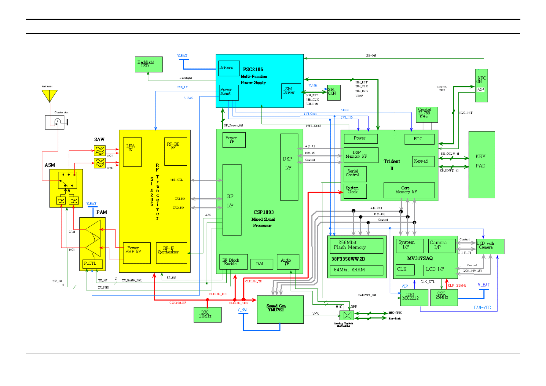
1. RF Solution Block Diagram
SAMSUNG Proprietary-Contents may change without notice
This Document can not be used without Samsung's authorization
6. SGH-E810 PCB Diagrams
6-1
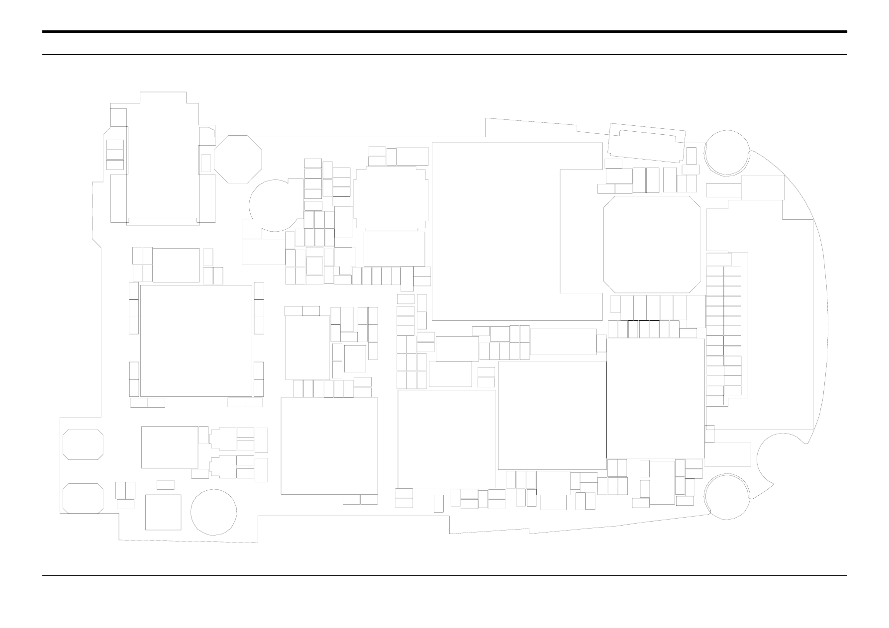
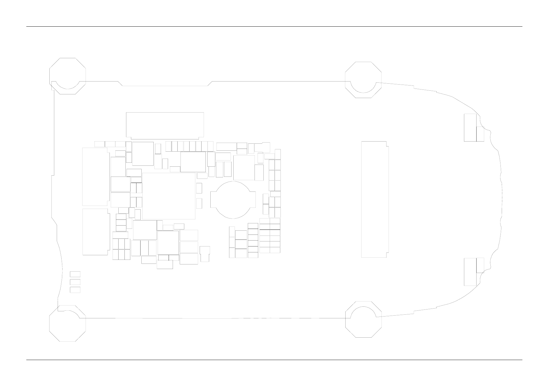
1.Main TOP Diagram
A
N
T
1
A
N
T
_
G
N
D
BAT1
C
1
0
4
C
1
0
5
C
1
0
6
C
1
0
7
C
1
0
8
C
1
0
9
C
1
1
0
C111
C
1
1
2
C
1
1
3
C
1
1
4
C
1
1
5
C116
C
1
1
7
C118
C119
C223
C
2
2
4
C
2
2
5
C226
C227
C
2
2
8
C229
C230
C231
C
2
3
2
C
2
3
3
C
2
3
4
C
2
3
5
C236
C
2
3
7
C
2
3
8
C
2
3
9
C
2
4
0
C
2
4
1
C242
C243
C244
C
2
4
5
C246
C247
C248
C249
C250
C
2
5
1
C
2
5
2
C
2
5
3
C
2
5
4
C255
C256
C257
C258
C259
C
2
6
0
C
2
6
1
C
2
6
2
C
3
0
0
C301
C
3
0
2
C
3
0
3
C
3
0
4
C
3
0
5
C306
C
3
0
7
C
3
0
8
C
3
0
9
C
3
1
0
C
3
1
2
C
3
1
3
C
3
1
4
C
3
1
5
C316
C317
C319
C320
C321
C
3
2
2
C323
C
3
2
5
C
3
2
7
C
3
2
8
C
3
2
9
C
3
3
0
C
3
3
1
C
3
3
2
C
3
3
3
C
3
3
4
C
3
3
5
C
3
3
6
C
4
0
0
C401
C402
C
4
0
3
C404
C405
C406
C
4
0
7
C408
C
4
1
1
C
4
1
2
C
4
1
3
C414
C
4
1
5
C416
C417
C418
C419
C420
C421
C
4
2
2
C423
C
4
2
4
C
4
2
5
C
4
2
6
C427
C428
C
4
2
9
C
4
3
0
C
4
3
1
C
4
3
2
C
4
3
3
C
4
3
4
C
4
3
5
C
N
1
0
0
C
N
1
0
1
C
N
2
0
1
CN400
D
3
0
0
G
1
G
2
G
3
G
4
L200
L
2
0
1
L
2
0
2
L
2
0
3
L
2
0
4
L
4
0
1
L
4
0
2
L
4
0
3
L
4
0
4
L
4
0
5
L
4
0
6
L
4
0
7
OSC300
O
S
C
4
0
0
Q200
Q
3
0
0
R
1
0
1
R102
R103
R104
R105
R106
R107
R108
R109
R110
R111
R112
R113
R114
R115
R116
R118
R124
R
1
2
5
R224
R
2
2
5
R
2
2
6
R
2
2
7
R
2
2
8
R
2
2
9
R
2
3
0
R
2
3
1
R
2
3
2
R233
R
2
3
4
R
2
3
5
R236
R
2
3
7
R238
R239
R
2
4
0
R241
R242
R243
R244
R245
R246
R
3
0
0
R302
R303
R
3
0
4
R
3
0
6
R
3
0
7
R
3
0
8
R
3
1
0
R311
R
3
1
2
R313
R
3
1
4
R
3
1
5
R
3
1
6
R400
R
4
0
1
R
4
0
2
R
4
0
3
R
4
0
4
R
4
0
5
R
4
0
6
R
4
0
7
R
4
0
8
R409
R
4
1
0
R
4
1
1
R
4
1
2
R413
U100
U
1
0
1
U200
U
2
0
1
U202
U300
U303
U
3
0
4
U306
U
4
0
0
U401
U
4
0
2
U
4
0
3
U
4
0
4
U405
ZD100
ZD101
ZD102
ZD103
ZD104
ZD105
ZD106
ZD107
ZD108
ZD109
ZD110
ZD111
ZD120
ZD121
ZD200
Z
D
2
0
1
Z
D
2
0
2
Z
D
2
0
3
ZD204
SAMSUNG Proprietary-Contents may change without notice
SGH-E810 PCB Diagrams
6-2
This Document can not be used without Samsung's authorization
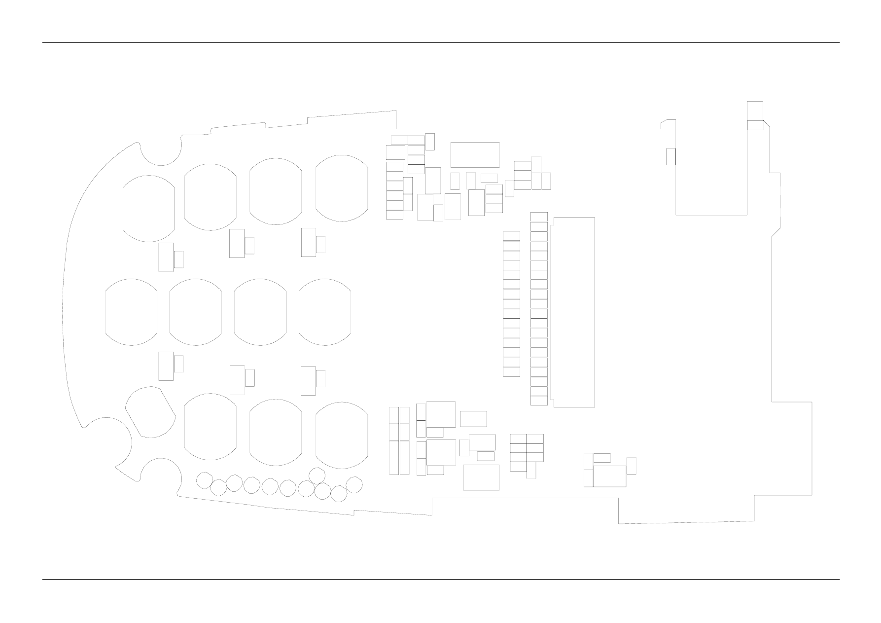
2. Main Bottom Diagram
*
0
1
2
3
4
5
6
7
8
9
C100
C101
C102
C103
C200
C201
C202
C203
C204
C205
C
2
0
6
C207
C208
C209
C
2
1
0
C211
C212
C213
C214
C
2
1
5
C216
C217
C218
C219
C220
C221
C222
C
2
6
3
C264
C
3
1
1
C
3
1
8
C
3
2
4
C326
C409
C410
C
N
2
0
0
C
P
_
T
C
K
C
P
_
T
D
I
C
P
_
T
D
O
C
P
_
T
M
S
C
P
_
W
E
N
D
S
P
_
T
C
K
D
S
P
_
T
D
I
D
S
P
_
T
D
O
D
S
P
_
T
M
S
F
1
F
2
F
3
F4
F
5
F6
L
3
0
0
L
E
D
1
0
0
L
E
D
1
0
1
L
E
D
1
0
2
L
E
D
1
0
3
L
E
D
1
0
4
L
E
D
1
0
5
Q
1
0
0
R100
R117
R
1
1
9
R
1
2
0
R
1
2
1
R
1
2
2
R123
R126
R
1
2
7
R128
R
1
2
9
R
1
3
0
R
1
3
1
R
1
3
2
R
1
3
3
R
1
3
4
R200
R
2
0
1
R202
R203
R204
R205
R
2
0
6
R207
R
2
0
8
R209
R210
R211
R212
R213
R214
R215
R216
R217
R218
R219
R220
R221
R222
R223
R
3
0
1
R
3
0
5
R
3
0
9
R
S
T
S
H
A
R
P
SW100
SW101
T
P
_
G
N
D
U
3
0
1
U
3
0
2
U305
V1
V10
V
1
1
V
1
2
V2
V3
V4
V5
V6
V7
V
8
V9
ZD112
Z
D
1
1
3
ZD114
Z
D
1
1
5
Z
D
1
1
6
Z
D
1
1
7
Z
D
1
1
8
Z
D
1
1
9
SAMSUNG Proprietary-Contents may change without notice
SGH-E810 PCB Diagrams
6-3
This Document can not be used without Samsung's authorization
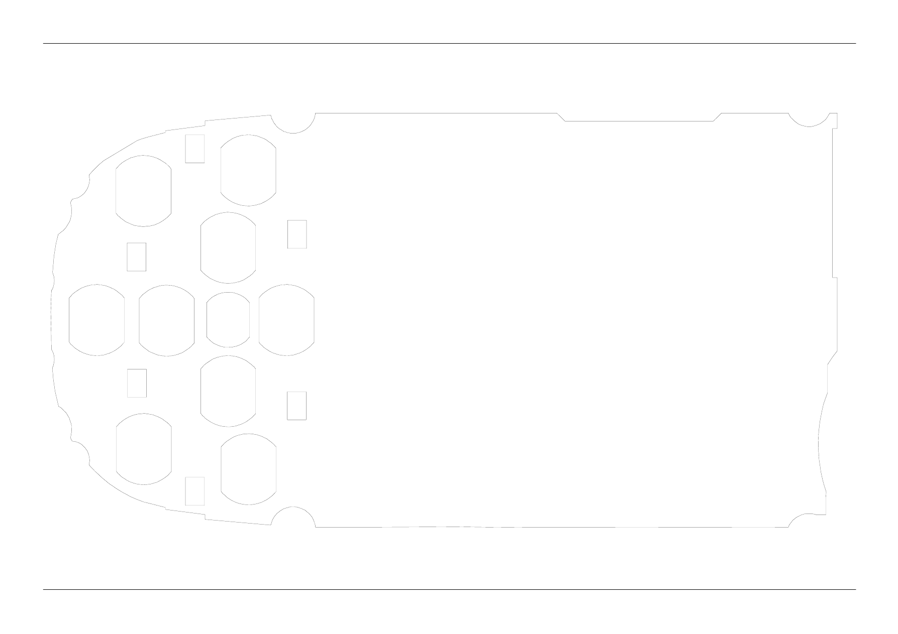
3.LCD TOP Diagram
C500
C501
C502
C
5
0
3
C504
C
5
0
5
C506
C507
C508
C509
C
5
1
0
C511
C
5
1
2
C
5
1
3
C
5
1
4
C
5
1
5
C516
C517
C518
C
5
1
9
C520
C
5
2
1
C
5
2
2
C
5
2
3
C524
C
5
2
5
C
5
2
6
C
5
2
7
C
5
2
8
C
5
2
9
C
5
3
0
C531
C532
C533
C
5
3
4
C
5
3
5
C
5
3
6
C
5
3
7
C
5
3
8
C
5
3
9
C
5
4
0
C
N
5
0
0
CN501
C
N
5
0
2
C
N
5
0
3
D
5
0
0
D501
D502
D
5
0
3
D
5
0
4
G
1
G
2
G
3
G
4
L
5
0
0
L501
L502
OSC500
Q
5
0
0
Q
5
0
1Q
5
0
2
Q503
Q
5
0
4
R
5
0
0
R501
R502
R
5
0
3
R504
R505
R506
R507
R508
R509
R510
R511
R512
R513
R514
R515
R516
R517
R518
R519
R520
R521
R522
R523
R524
R
5
2
5
R
5
2
6
R527
R
5
2
8
R529
R
5
3
0
R
5
3
1
R
5
3
2
R533
R
5
3
4
R
5
3
5
R
5
3
6
S
D
5
0
0
SD501
S
D
5
0
2
U500
U
5
0
1
U502
U
5
0
3
U504
Z
D
5
0
0
Z
D
5
0
1
Z
D
5
0
2
Z
D
5
0
3
Z
D
5
0
4
Z
D
5
0
5
Z
D
5
0
6
Z
D
5
0
7Z
D
5
0
8
Z
D
5
0
9
ZD510
Z
D
5
1
1
Z
D
5
1
2
Z
D
5
1
3
Z
D
5
1
4
Z
D
5
1
5
Z
D
5
1
6
ZD517
ZD518
Z
D
5
1
9
Z
D
5
2
0
Z
D
5
2
1
Z
D
5
2
2
SAMSUNG Proprietary-Contents may change without notice
SGH-E810 PCB Diagrams
6-4
This Document can not be used without Samsung's authorization
4.LCD TOP Diagram
C
L
E
A
R
D
O
W
N
I
LED500
LED501
LED502
LED503
LED504
LED505
L
E
F
T
M
E
N
U
P
W
R
R
IG
H
T
S
E
N
D
S
T
O
U
P

ELECTRONICS
Samsung Electronics Co.,Ltd. JULY. .2004
Printed in Korea.
Code No.: GH68-05709A
BASIC.
ⓒ
This Service Manual is a property of Samsung Electronics Co.,Ltd.
Any unauthorized use of Manual can be punished under applicable
International and/or domestic law.
Wyszukiwarka
Podobne podstrony:
PANsound manual
als manual RZ5IUSXZX237ENPGWFIN Nieznany
hplj 5p 6p service manual vhnlwmi5rxab6ao6bivsrdhllvztpnnomgxi2ma vhnlwmi5rxab6ao6bivsrdhllvztpnnomg
BSAVA Manual of Rabbit Surgery Dentistry and Imaging
Okidata Okipage 14e Parts Manual
Bmw 01 94 Business Mid Radio Owners Manual
Manual Acer TravelMate 2430 US EN
manual mechanika 2 2 id 279133 Nieznany
4 Steyr Operation and Maintenance Manual 8th edition Feb 08
Oberheim Prommer Service Manual
cas test platform user manual
Kyocera FS 1010 Parts Manual
juki DDL 5550 DDL 8500 DDL 8700 manual
Forex Online Manual For Successful Trading
ManualHandlingStandingAssessment
Brother PT 2450 Parts Manual
więcej podobnych podstron