DATA SHEET
Product specification
Supersedes data of April 1995
File under Discrete Semiconductors, SC13b
1997 Jun 19
DISCRETE SEMICONDUCTORS
BSS92
P-channel enhancement mode
vertical D-MOS transistor
1997 Jun 19
2
Philips Semiconductors
Product specification
P-channel enhancement mode
vertical D-MOS transistor
BSS92
FEATURES
•
Direct interface to C-MOS, TTL, etc.
•
High-speed switching
•
No secondary breakdown.
APPLICATIONS
•
Line current interrupter in telephony applications
•
Relay, high speed and line transformer drivers.
DESCRIPTION
P-channel enhancement mode vertical D-MOS transistor
in a TO-92 (SOT54) variant package.
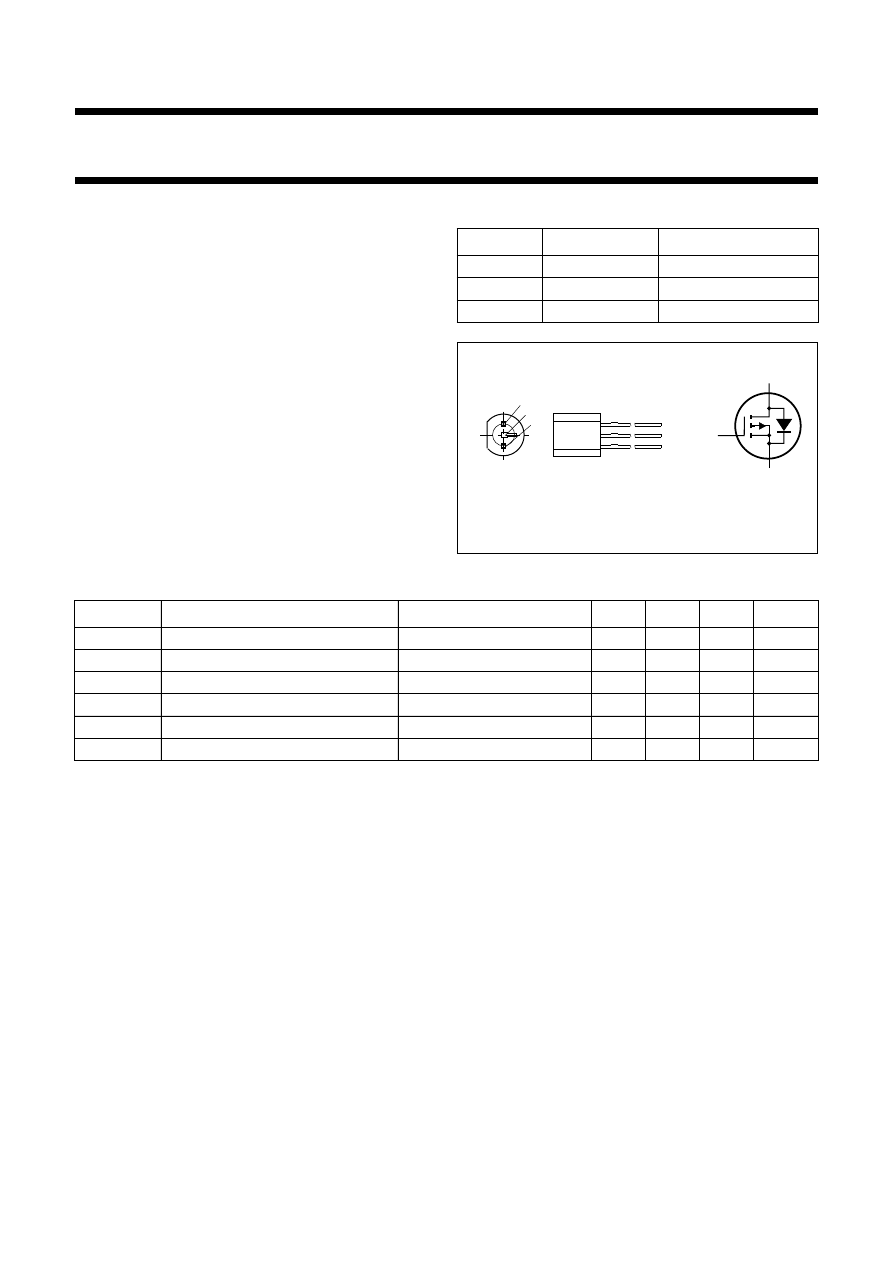
PINNING - TO-92 (SOT54) variant
PIN
SYMBOL
DESCRIPTION
1
g
gate
2
d
drain
3
s
source
Fig.1 Simplified outline and symbol.
handbook, halfpage
s
d
g
MAM144
1
3
2
QUICK REFERENCE DATA
SYMBOL
PARAMETER
CONDITIONS
MIN.
TYP.
MAX.
UNIT
V
DS
drain-source voltage (DC)
−
−
−
240
V
V
GSO
gate-source voltage (DC)
open drain
−
−
±
20
V
I
D
drain current (DC)
−
−
−
150
mA
R
DSon
drain-source on-state resistance
I
D
=
−
100 mA; V
GS
=
−
10 V
−
10
20
Ω
P
tot
total power dissipation
T
amb
≤
25
°
C
−
−
1
W
y
fs
forward transfer admittance
V
DS
=
−
25 V; I
D
=
−
100 mA
60
200
−
mS
1997 Jun 19
3
Philips Semiconductors
Product specification
P-channel enhancement mode
vertical D-MOS transistor
BSS92
LIMITING VALUES
In accordance with the Absolute Maximum Rating System (IEC 134).
THERMAL CHARACTERISTICS
Note to the Limiting values and Thermal characteristics
1. Device mounted on a printed-circuit board, maximum lead length 4 mm; mounting pad for drain lead minimum
10 mm
×
10 mm.
CHARACTERISTICS
T
j
= 25
°
C unless otherwise specified.
SYMBOL
PARAMETER
CONDITIONS
MIN.
MAX.
UNIT
V
DS
drain-source voltage (DC)
−
−
240
V
V
GSO
gate-source voltage (DC)
open drain
−
±
20
V
I
D
drain current (DC)
−
−
150
mA
I
DM
peak drain current
−
−
600
mA
P
tot
total power dissipation
T
amb
≤
25
°
C; note 1
−
1
W
T
stg
storage temperature
−
55
+150
°
C
T
j
operating junction temperature
−
150
°
C
SYMBOL
PARAMETER
CONDITIONS
VALUE
UNIT
R
th j-a
thermal resistance from junction to ambient
note 1
125
K/W
SYMBOL
PARAMETER
CONDITIONS
MIN.
TYP.
MAX.
UNIT
V
(BR)DSS
drain-source breakdown voltage
V
GS
= 0; I
D
=
−
250
µ
A
−
240
−
−
V
V
GSth
gate-source threshold voltage
V
DS
= V
GS
; I
D
=
−
1 mA
−
0.8
−
−
2.8
V
I
DSS
drain-source leakage current
V
GS
= 0; V
DS
=
−
60 V
−
−
−
200
nA
V
GS
= 0; V
DS
=
−
200 V
−
−
−
60
µ
A
I
GSS
gate leakage current
V
DS
= 0; V
GS
=
±
20 V
−
−
±
100
nA
R
DSon
drain-source on-state resistance
V
GS
=
−
10 V; I
D
=
−
100 mA
−
10
20
Ω
y
fs
forward transfer admittance
V
DS
=
−
25 V; I
D
=
−
100 mA
60
200
−
mS
C
iss
input capacitance
V
GS
= 0; V
DS
=
−
25 V; f = 1 MHz
−
65
−
pF
C
oss
output capacitance
V
GS
= 0; V
DS
=
−
25 V; f = 1 MHz
−
20
−
pF
C
rss
reverse transfer capacitance
V
GS
= 0; V
DS
=
−
25 V; f = 1 MHz
−
6
−
pF
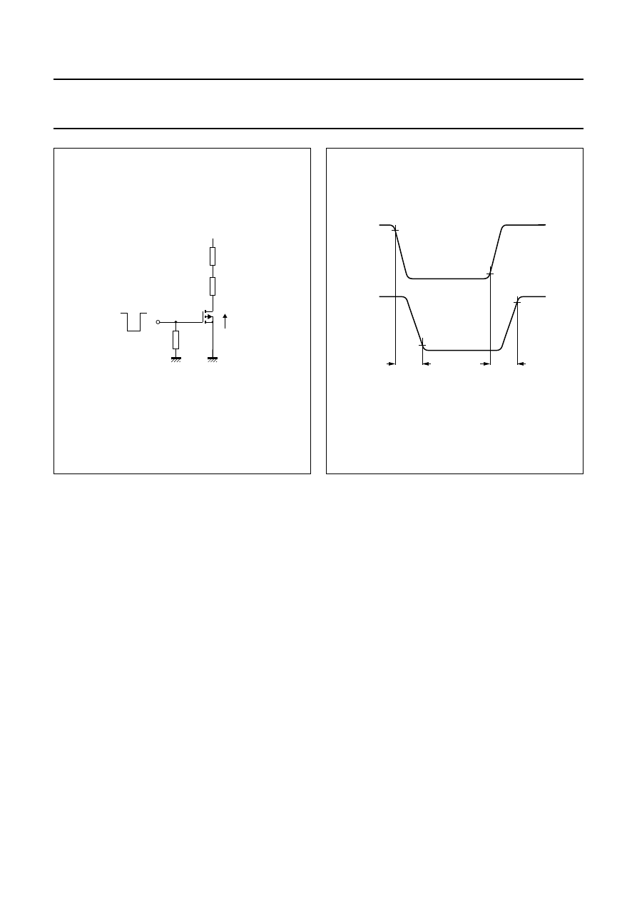
Switching times (see Figs 2 and 3)
t
on
turn-on time
V
GS
= 0 to
−
10 V; V
DD
=
−
50 V;
I
D
=
−
250 mA
−
5
−
ns
t
off
turn-off time
V
GS
=
−
10 to 0 V; V
DD
=
−
50 V;
I
D
=
−
250 mA
−
20
−
ns
1997 Jun 19
4
Philips Semiconductors
Product specification
P-channel enhancement mode
vertical D-MOS transistor
BSS92
Fig.2 Switching times test circuit.
handbook, halfpage
MBB689
50
Ω
I D
−
10 V
0
V =
−
50 V
DD
Fig.3 Input and output waveforms.
handbook, halfpage
MBB690
10 %
90 %
90 %
10 %
t on
t off
OUTPUT
INPUT
1997 Jun 19
5
Philips Semiconductors
Product specification
P-channel enhancement mode
vertical D-MOS transistor
BSS92
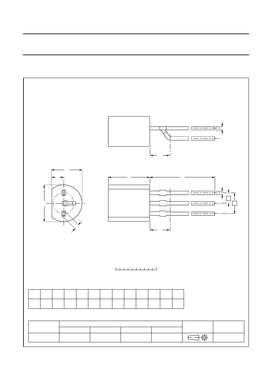
PACKAGE OUTLINE
UNIT
A
REFERENCES
OUTLINE
VERSION
EUROPEAN
PROJECTION
ISSUE DATE
IEC
JEDEC
EIAJ
mm
5.2
5.0
b
0.48
0.40
c
0.45
0.40
D
4.8
4.4
d
1.7
1.4
E
4.2
3.6
L
14.5
12.7
e
2.54
e1
1.27
L1
(1)
max
L2
max
2.5
2.5
b1
0.66
0.56
DIMENSIONS (mm are the original dimensions)
Notes
1. Terminal dimensions within this zone are uncontrolled to allow for flow of plastic and terminal irregularities.
SOT54 variant
TO-92
SC-43
A
L
0
2.5
5 mm
scale
b
c
D
b
1
L1
d
E
Plastic single-ended leaded (through hole) package; 3 leads (on-circle)
SOT54 variant
1
2
3
L2
e1
e
97-04-14

1997 Jun 19
6
Philips Semiconductors
Product specification
P-channel enhancement mode
vertical D-MOS transistor
BSS92
DEFINITIONS
LIFE SUPPORT APPLICATIONS
These products are not designed for use in life support appliances, devices, or systems where malfunction of these
products can reasonably be expected to result in personal injury. Philips customers using or selling these products for
use in such applications do so at their own risk and agree to fully indemnify Philips for any damages resulting from such
improper use or sale.
Data Sheet Status
Objective specification
This data sheet contains target or goal specifications for product development.
Preliminary specification
This data sheet contains preliminary data; supplementary data may be published later.
Product specification
This data sheet contains final product specifications.
Limiting values
Limiting values given are in accordance with the Absolute Maximum Rating System (IEC 134). Stress above one or
more of the limiting values may cause permanent damage to the device. These are stress ratings only and operation
of the device at these or at any other conditions above those given in the Characteristics sections of the specification
is not implied. Exposure to limiting values for extended periods may affect device reliability.
Application information
Where application information is given, it is advisory and does not form part of the specification.

1997 Jun 19
7
Philips Semiconductors
Product specification
P-channel enhancement mode vertical
D-MOS transistor
BSS92
NOTES

Internet: http://www.semiconductors.philips.com
Philips Semiconductors – a worldwide company
© Philips Electronics N.V. 1997
SCA54
All rights are reserved. Reproduction in whole or in part is prohibited without the prior written consent of the copyright owner.
The information presented in this document does not form part of any quotation or contract, is believed to be accurate and reliable and may be changed
without notice. No liability will be accepted by the publisher for any consequence of its use. Publication thereof does not convey nor imply any license
under patent- or other industrial or intellectual property rights.
Netherlands: Postbus 90050, 5600 PB EINDHOVEN, Bldg. VB,
Tel. +31 40 27 82785, Fax. +31 40 27 88399
New Zealand: 2 Wagener Place, C.P.O. Box 1041, AUCKLAND,
Tel. +64 9 849 4160, Fax. +64 9 849 7811
Norway: Box 1, Manglerud 0612, OSLO,
Tel. +47 22 74 8000, Fax. +47 22 74 8341
Philippines: Philips Semiconductors Philippines Inc.,
106 Valero St. Salcedo Village, P.O. Box 2108 MCC, MAKATI,
Metro MANILA, Tel. +63 2 816 6380, Fax. +63 2 817 3474
Poland: Ul. Lukiska 10, PL 04-123 WARSZAWA,
Tel. +48 22 612 2831, Fax. +48 22 612 2327
Portugal: see Spain
Romania: see Italy
Russia: Philips Russia, Ul. Usatcheva 35A, 119048 MOSCOW,
Tel. +7 095 755 6918, Fax. +7 095 755 6919
Singapore: Lorong 1, Toa Payoh, SINGAPORE 1231,
Tel. +65 350 2538, Fax. +65 251 6500
Slovakia: see Austria
Slovenia: see Italy
South Africa: S.A. PHILIPS Pty Ltd., 195-215 Main Road Martindale,
2092 JOHANNESBURG, P.O. Box 7430 Johannesburg 2000,
Tel. +27 11 470 5911, Fax. +27 11 470 5494
South America: Rua do Rocio 220, 5th floor, Suite 51,
04552-903 São Paulo, SÃO PAULO - SP, Brazil,
Tel. +55 11 821 2333, Fax. +55 11 829 1849
Spain: Balmes 22, 08007 BARCELONA,
Tel. +34 3 301 6312, Fax. +34 3 301 4107
Sweden: Kottbygatan 7, Akalla, S-16485 STOCKHOLM,
Tel. +46 8 632 2000, Fax. +46 8 632 2745
Switzerland: Allmendstrasse 140, CH-8027 ZÜRICH,
Tel. +41 1 488 2686, Fax. +41 1 481 7730
Taiwan: Philips Semiconductors, 6F, No. 96, Chien Kuo N. Rd., Sec. 1,
TAIPEI, Taiwan Tel. +886 2 2134 2865, Fax. +886 2 2134 2874
Thailand: PHILIPS ELECTRONICS (THAILAND) Ltd.,
209/2 Sanpavuth-Bangna Road Prakanong, BANGKOK 10260,
Tel. +66 2 745 4090, Fax. +66 2 398 0793
Turkey: Talatpasa Cad. No. 5, 80640 GÜLTEPE/ISTANBUL,
Tel. +90 212 279 2770, Fax. +90 212 282 6707
Ukraine: PHILIPS UKRAINE, 4 Patrice Lumumba str., Building B, Floor 7,
252042 KIEV, Tel. +380 44 264 2776, Fax. +380 44 268 0461
United Kingdom: Philips Semiconductors Ltd., 276 Bath Road, Hayes,
MIDDLESEX UB3 5BX, Tel. +44 181 730 5000, Fax. +44 181 754 8421
United States: 811 East Arques Avenue, SUNNYVALE, CA 94088-3409,
Tel. +1 800 234 7381
Uruguay: see South America
Vietnam: see Singapore
Yugoslavia: PHILIPS, Trg N. Pasica 5/v, 11000 BEOGRAD,
Tel. +381 11 625 344, Fax.+381 11 635 777
For all other countries apply to: Philips Semiconductors, Marketing & Sales Communications,
Building BE-p, P.O. Box 218, 5600 MD EINDHOVEN, The Netherlands, Fax. +31 40 27 24825
Argentina: see South America
Australia: 34 Waterloo Road, NORTH RYDE, NSW 2113,
Tel. +61 2 9805 4455, Fax. +61 2 9805 4466
Austria: Computerstr. 6, A-1101 WIEN, P.O. Box 213,
Tel. +43 1 60 101, Fax. +43 1 60 101 1210
Belarus: Hotel Minsk Business Center, Bld. 3, r. 1211, Volodarski Str. 6,
220050 MINSK, Tel. +375 172 200 733, Fax. +375 172 200 773
Belgium: see The Netherlands
Brazil: see South America
Bulgaria: Philips Bulgaria Ltd., Energoproject, 15th floor,
51 James Bourchier Blvd., 1407 SOFIA,
Tel. +359 2 689 211, Fax. +359 2 689 102
Canada: PHILIPS SEMICONDUCTORS/COMPONENTS,
Tel. +1 800 234 7381
China/Hong Kong: 501 Hong Kong Industrial Technology Centre,
72 Tat Chee Avenue, Kowloon Tong, HONG KONG,
Tel. +852 2319 7888, Fax. +852 2319 7700
Colombia: see South America
Czech Republic: see Austria
Denmark: Prags Boulevard 80, PB 1919, DK-2300 COPENHAGEN S,
Tel. +45 32 88 2636, Fax. +45 31 57 0044
Finland: Sinikalliontie 3, FIN-02630 ESPOO,
Tel. +358 9 615800, Fax. +358 9 61580920
France: 4 Rue du Port-aux-Vins, BP317, 92156 SURESNES Cedex,
Tel. +33 1 40 99 6161, Fax. +33 1 40 99 6427
Germany: Hammerbrookstraße 69, D-20097 HAMBURG,
Tel. +49 40 23 53 60, Fax. +49 40 23 536 300
Greece: No. 15, 25th March Street, GR 17778 TAVROS/ATHENS,
Tel. +30 1 4894 339/239, Fax. +30 1 4814 240
Hungary: see Austria
India: Philips INDIA Ltd, Shivsagar Estate, A Block, Dr. Annie Besant Rd.
Worli, MUMBAI 400 018, Tel. +91 22 4938 541, Fax. +91 22 4938 722
Indonesia: see Singapore
Ireland: Newstead, Clonskeagh, DUBLIN 14,
Tel. +353 1 7640 000, Fax. +353 1 7640 200
Israel: RAPAC Electronics, 7 Kehilat Saloniki St, PO Box 18053,
TEL AVIV 61180, Tel. +972 3 645 0444, Fax. +972 3 649 1007
Italy: PHILIPS SEMICONDUCTORS, Piazza IV Novembre 3,
20124 MILANO, Tel. +39 2 6752 2531, Fax. +39 2 6752 2557
Japan: Philips Bldg 13-37, Kohnan 2-chome, Minato-ku, TOKYO 108,
Tel. +81 3 3740 5130, Fax. +81 3 3740 5077
Korea: Philips House, 260-199 Itaewon-dong, Yongsan-ku, SEOUL,
Tel. +82 2 709 1412, Fax. +82 2 709 1415
Malaysia: No. 76 Jalan Universiti, 46200 PETALING JAYA, SELANGOR,
Tel. +60 3 750 5214, Fax. +60 3 757 4880
Mexico: 5900 Gateway East, Suite 200, EL PASO, TEXAS 79905,
Tel. +9-5 800 234 7381
Middle East: see Italy
Printed in The Netherlands
137107/00/02/pp8
Date of release: 1997 Jun 19
Document order number:
9397 750 02335
Wyszukiwarka
Podobne podstrony:
philips chassis l6 1
AWB982PH PHILIPS WHIRLPOOL
AWB9771GR PHILIPS WHIRLPOOL
AWG759 PHILIPS WHIRLPOOL
AWB9211 PHILIPS WHIRLPOOL
philips tv25pt5322 58 dfu pol
PHILIPS CAM101 pl
AWG779 PHILIPS WHIRLPOOL
PHILIPS DSX 6010 instrukcja obslugi
AWG736 PHILIPS WHIRLPOOL
ICM7555 Philips
PHILIPS DSB instrukcja obslugi
AWG779PH PHILIPS WHIRLPOOL
instrukcja obsługi elektrycznej maszynki do strzyżenia włosów Philips QC 5053, QC 5050, QC 5010 po p
Philips 2196
PhilipKDick MozemyCieZbudowac
AWG734PH PHILIPS WHIRLPOOL
więcej podobnych podstron