
Damage buildup and recovery in III–V compound
semiconductors at low temperatures
A. Turos
a,b,*
, A. Stonert
a
, L. Nowicki
a
, R. Ratajczak
a
,
E. Wendler
c
, W. Wesch
c
a
Soltan Institute of Nuclear Studies, 05-400 S´wierk/Otwock, Poland
b
Institute of Electronic Materials Technology, 01-919 Warsaw, ul. Wolczynska 133, Poland
c
Friedrich Schiller University, 07743 Jena, Max-Wien-Platz 1, Germany
Available online 1 August 2005
Abstract
Results are presented of the RBS/channeling study of the structural defect behavior in ion bombarded
In
x
Ga
1
x
As
y
P
1
y
(0 6 x, y 6 1) compounds at temperatures ranging from 15 K (LT) to 300 K (RT). Experiments con-
sisted of implantation with different ions to fluences ranging from 4
· 10
13
to 5
· 10
15
at./cm
2
at different temperatures
followed by in situ RBS/channeling measurements. Successive measurements of LT implanted samples were performed
during warming up to RT.
Broad recovery stage beginning at 100 K for all compounds was revealed. It was attributed to the defect mobility in
the group III sublattice. Steep damage buildup up to amorphisation with increasing ion dose was observed. The defect
production efficiency is much higher at LT than at RT. The consequences of defect mobility at RT for ion implanted
semiconductor structures are discussed.
2005 Elsevier B.V. All rights reserved.
PACS: 61.80.Jh; 68.55.Jk; 68.55.Ln; 61.10.Nz
Keywords: III–V semiconductor compounds; Defects; Ion implantation; RBS/channeling
1. Introduction
Modification of semiconductor properties by
ion implantation is a well-established technologi-
cal process. For structures based on compound
semiconductors it is used for introducing active
doping, compositional mixing of quantum wells
0168-583X/$ - see front matter
2005 Elsevier B.V. All rights reserved.
doi:10.1016/j.nimb.2005.06.097
*
Corresponding author. Address: Institute of Electronic
Materials Technology, 01-919 Warsaw, ul. Wolczynska 133,
Poland. Tel.: +48 603 092223; fax: +48 8645496.
E-mail address:
(A. Turos).
Nuclear Instruments and Methods in Physics Research B 240 (2005) 105–110
www.elsevier.com/locate/nimb
and formation of isolation regions in electronic de-
vices. Point defects and their complexes determine
optical and electrical properties of semiconduc-
tors, diffusion of impurities as well as the recovery
of crystalline lattice after ion bombardment and
subsequent annealing.
Broad recovery stage at low temperatures exists
for III–V semiconductor compounds
. It is
located between 100 K and 400 K and is attributed
to the recombination or reconfiguration of a
variety of defects with different activation energy.
Thus, the investigation of thermally activated
processes can be decisive for identification of de-
fects. On the other hand defect mobility at RT
can lead to important effect transformation after
RT implantation and subsequent storage. Hence,
structure and distribution of radiation defects
are of great scientific and technological interest
and their reproducible control is crucial for elec-
trical and structural properties of implanted
materials.
In this paper we review the results of the study
of defect buildup and recovery in arsenide and
phosphide semiconductor compounds after ion
implantation at temperatures below 50 K and sub-
sequent warming up to RT. This process was mon-
itored by in situ RBS/channeling measurements.
Since the main objective of this workwas to eluci-
date the properties of point defects and their com-
plexes light ion bombardment was applied. Light
ions produce principally diluted binary collision
cascades and are well suited for the study of simple
defects.
2. Experimental
In
x
Ga
1
x
As
y
P
1
y
(0 6 x, y 6 1) binary, ternary
and quaternary compound semiconductors were
studied. Epitaxial layers of these compounds were
grown using the MOCVD technique in the Aix-
tron AIX200RD reactor at the Institute of Elec-
tronic Materials Technology, Warsaw on
h1 0 0i
semi-insulating GaAs and InP substrates. These
were: InP, In
0.53
Ga
0.47
As, In
0.82
Ga
0.18
As
0.52
P
0.48
.
Layers of such compositions are lattice matched
to InP substrates and consequently they are not
strained due to the pseoudomorphic growth.
Energy (keV)
600
800
1000
1200
Yield
0
500
1000
1500
2000
Random
10E12
4E12
2E12
1E12
Virgin
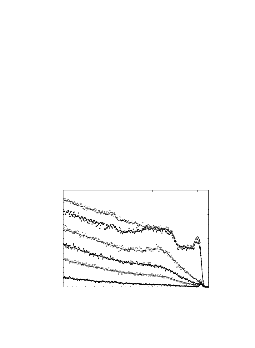
Fig. 1.
h1 0 0i aligned spectra measured in situ for In
x
Ga
1
x
As
y
P
1
y
(x = 0.82, y = 0.52) epitaxial layer before and after implantation
to different fluences of 150 keV N ions at 15 K. The spectra are labeled with fluences in 10
13
at./cm
2
.
106
A. Turos et al. / Nucl. Instr. and Meth. in Phys. Res. B 240 (2005) 105–110
Fluence (1x10
13
at/cm
2
)
0
10
20
30
40
50
60
70
80
Amorphous fraction
0.0
0.5
1.0
InGaAsP - 15 K
InGaAs -15 K
InP - 15 K
InGaAsP - RT
Fig. 2. Damage buildup in different semiconductor compounds upon N-ion implantation at 15 K. Also shown is the similar curve for
InGaAsP measured after RT implantation.
T
a
(K)
0
100
200
300
N
d
(15K)/N
d
(T
a
)
0.0
0.2
0.4
0.6
0.8
1.0
1.2
InP
GaAs
InGaAs
InGaAsP
After
24 hr
Fig. 3. Defect recovery in various semiconductor compounds during warming from 15 K to up 295 K. The solid lines are drawn to
guide the eye.
A. Turos et al. / Nucl. Instr. and Meth. in Phys. Res. B 240 (2005) 105–110
107
Experiments were carried out using the Romeo
and Julia two beam facility at Institute of Solid
State Physics, FSU Jena. The beam delivered by
the ion implanter Romeo were used to produce de-
fects, while the tandem accelerator Julia equipped
with a 3-axis goniometer was applied for in situ
ion-channeling (RBS/c) measurements. The exper-
iments were carried out following two schemes:
(i) Epitaxial layers were implanted to increasing
fluences of 150 keV N
+
ions at two tempe-
ratures (15 K–50 K) and RT until amorphi-
sation was attained; damage buildup was
monitored by in situ RBS/c measurements.
In order to avoid sample heating upon ion
implantation beam current density was kept
below 1 lA/cm
2
.
(ii) Implanted at low temperatures epitaxial
layers were analyzed in situ by RBS/c with
1.4 MeV
4
He ions and stepwise warmed up
to RT. At each selected temperature the sam-
ple was stored for 10 min and then cooled
down to 15 K where aligned RBS/c spectra
were measured. Subsequently, the sample
was warmed to the next preset temperature
and the whole procedure was repeated.
The evaluation of channeling data measured at
different temperatures requires consideration of
several usually neglected factors, like changes of
thermal vibration amplitudes of crystal atoms
and defect production or removal by the analyzing
beam. The Monte Carlo computer code McChasy
described in detail elsewhere
was used for the
purpose.
3. Results
shows the
h1 0 0i aligned spectra for a In
x
-
Ga
1
x
As
y
P
1
y
(x = 0.82, y = 0.52), epitaxial layer
taken at 15 K prior to and after ion implantation
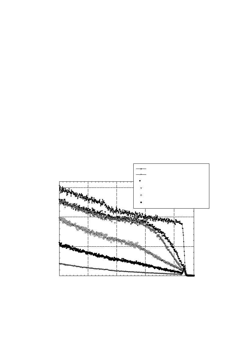
Channel number
400
500
600
700
800
Y
ield
0
1000
2000
3000
Random
Virgin
1E13 As/cm
2
as implanted
1E13 As/cm
2
after 2 months at RT
1E12 As/cm
2
as implanted
1E12 As/cm
2
after 2 months at RT
Fig. 4. Random and
h1 0 0i aligned RBS spectra for InP single crystal prior and after 1.2 MeV As-ion implantation to different fluences
and after prolonged storage at RT.
108
A. Turos et al. / Nucl. Instr. and Meth. in Phys. Res. B 240 (2005) 105–110
to different fluences of 150 keV N ions. Typical
damage peakthat forms upon ion implantation
is in this case composed of four peaks each corre-
sponding to a different sublattice. Damage profiles
for each sublattice were calculated by fitting simu-
lated spectra to the experimental ones yielding the
damage buildup curve shown in
. There is a
small difference in defect production efficiency at
LT between different In concentration containing
compounds. The damage ingrowth is much slower
for RT ion implantation. Here again the difference
between the studied compounds is rather small.
Temperature dependence of defect production effi-
ciency is a strong indication that important defect
transformations occur at temperatures below RT.
shows damage recovery curve for samples
implanted at LT. For all studied compounds
broad recovery stage begins at approximately
100 K and extends above RT. Although our exper-
imental setup does not allow direct measurements
above RT the prolonged storage at RT after
warming up of a sample implanted at LT leads
to the further reduction of defect content. For
comparison similar recovery curve for GaAs is
also plotted in
.
Defect mobility at RT has profound conse-
quences on properties of ion implanted semicon-
ductor
structures.
shows
channeling
spectra for InP single crystal implanted in random
direction at RT to different fluences of 1.2 MeV As
ions. After prolonged storage at RT important
damage reduction was clearly visible. Damage
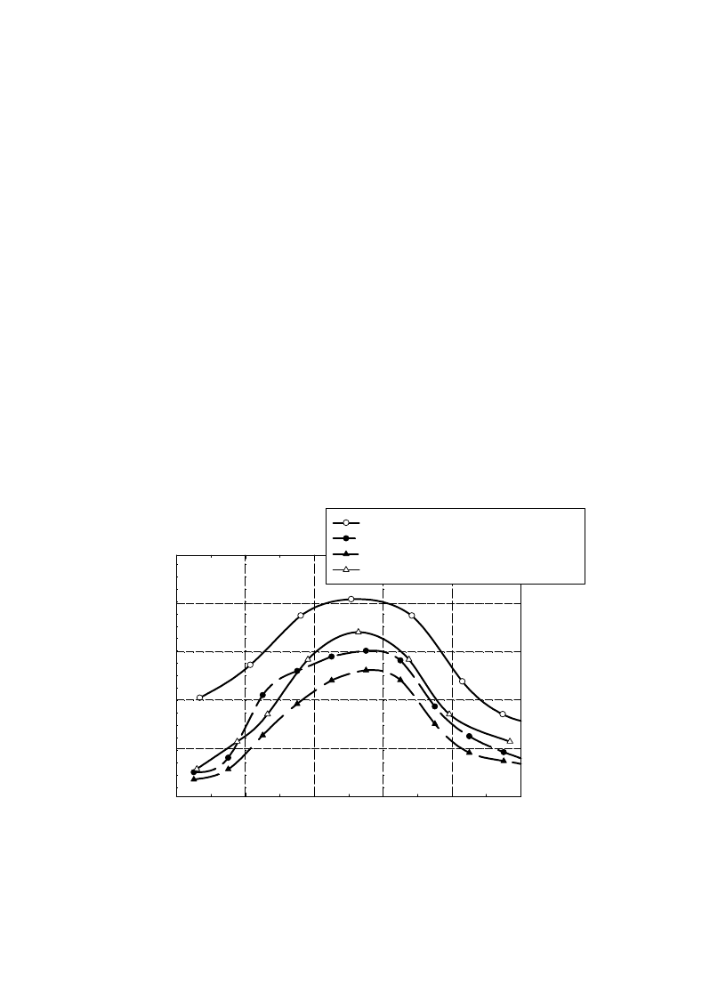
depth profiles calculated from these spectra and
corresponding lattice strain profiles determined
by high resolution X-ray diffraction (HRXRD)
are shown in
. One notes a strong corre-
lation between RBS/channeling and HRXRD
data.
4. Discussion and conclusions
Despite considerable workin recent years the
defect structure development in ion-irradiated
Depth (nm)
0
200
400
600
800
1000
-∆
a/a (ppm)
0
200
400
600
800
1000
Defect Concentration (at.%)
0
20
40
60
80
100
1E13 As/cm
2
XRD as implanted
1E13 As/cm
2
RBS/c as implanted
1E13 As/cm
2
RBS/c after 6 months at RT
1E13 As/cm
2
XRD after 6 months at RT
Fig. 5. Damage depth distribution for InP single crystal implanted with 1.2 MeV As ions to different fluences and the corresponding
strain profile for as implanted samples and after prolonged storage at RT. Note that the strain is negative, i.e. the implanted layer is
under tensile stress.
A. Turos et al. / Nucl. Instr. and Meth. in Phys. Res. B 240 (2005) 105–110
109

III–V semiconductor compounds is not well
understood. Although ion bombardment processes
in InP have been studied quite extensively over the
last decade, there remains a lackof understanding
of the fundamental mechanism of dynamic anneal-
ing that controls the damage buildup, amorphisa-
tion and annealing in other In-based compounds.
There is a general agreement that high concentra-
tions of Frenkel pairs can be frozen in during low
temperature irradiations and that defects in the
two sublattices react independently. Those that an-
neal below room temperature are related to the
group III sublattice whereas the group V intersti-
tials become mobile at approximately 500 K. Pos-
itron annihilation spectroscopy confirmed that the
large annealing stage between 100 K and 300 K is
due to the mobility of In vacancies and their sub-
sequent recombination with In interstitials
Recombination with P interstitials is also possible
leading to the formation of antisite defects. The
fact that this occurs in a quite large temperature
range suggests that a variety of trapping centers
of both kinds of interstitials is involved. Defects
that survive well above room temperature belong
principally to the group V sublattice.
There is only a small difference in damage build-
up in for all studied compounds. Akano et al.
observed that InP can be more easily amorphised
than InGaAs upon O-ion bombardment at 80 K.
At the present it is not clear whether this difference
can be attributed to the ion itself or to their less
accurate method of spectra analysis. Damage
recovery at low temperatures reveals much impor-
tant differences: the fastest recovery was observed
for InGaAsP whereas it is slowest in InP. Conse-
quently the residual damage at RT amounts to
40% of the initial one as compared to 18% for
InGaAs. This is apparently related to the kind
of formed defects which are unknown at the
moment.
The great mobility of group III interstitials has
important consequences in the practice. Shelf stor-
age of ion implanted semiconductor structures,
even the processed ones, can produce important
changes of their properties. Defect presence influ-
ences directly the conductivity and defect induced
strain modifies the bandgap.
References
[1] S.T. Picraux, Radiat. Effects 17 (1973) 261.
[2] D. Stievenard, X. Boddaert, J.C. Bourgoin, H.J. von
Bardeleben, Phys. Rev. B 41 (1990) 5271.
[3] A. Stonert, A. Turos, B. Breeger, E. Wendler, W. Wesch,
Mod. Phys. Lett. B 15 (2001) 1437.
[4] K. Karsten, P. Ehrhart, Phys. Rev. B 51 (1995) 10508.
[5] L. Nowicki, A. Turos, R. Ratajczak, A. Stonert, F. Garrido,
these Proceedings,
doi:10.1016/j.nimb.2005.06.129
[6] A. Turos, J. Gaca, M. Wojcik, L. Nowicki, R. Ratajczak, R.
Groetzschel, F. Eichhorn, N. Schell, Nucl. Instr. and Meth.
B 219–220 (2004) 618.
[7] M. To¨rnquist, J. Nissila, F. Kiessling, C. Corbel, P.
Hautoja¨rvi, Mater. Sci. Forum 143–147 (1994) 347.
[8] U.G. Akano, I.V. Mitchell, F.R. Shepherd, C.J. Miner,
Nucl. Instr. and Meth. B 106 (2004) 618.
110
A. Turos et al. / Nucl. Instr. and Meth. in Phys. Res. B 240 (2005) 105–110
Document Outline
Wyszukiwarka
Podobne podstrony:
12 i 13 (2005 06)
psychozy alkoholowe 13.11.2005, Studia, Psychoprofilaktyka
Mózgowie2004 2005 13 05
Mózgowie2004 2005 13 05 2
kk, ART 220 KK, III KK 23/05 - postanowienie z dnia 13 kwietnia 2005 r
kks, ART 91 KKS, III KK 134/04 - postanowienie z dnia 13 kwietnia 2005 r
PRAKTYKA wrzesień 2005, 2P 34 KOSZYKÓWKA IVa 13, Konspekt lekcji piłki ręcznej dla kl
podatki, wn zwr nadpl podat 2, Garwolin, 13 czerwca 2005 r
PRAKTYKA wrzesień 2005, 1P 12 NOŻNA IVb 13, Konspekt lekcji piłki ręcznej dla kl
13 407 pol ed02 2005
Aptekarz 2005 13 suplement
2005 04 13
psychozy alkoholowe 13.11.2005, Studia, Psychoprofilaktyka
Mózgowie2004 2005 13 05
Mózgowie2004 2005 13 05 2
Mózgowie2004 2005 13 05 2
więcej podobnych podstron