AVR131: Using the AVR’s High-speed PWM
Features
•
Analog Waveform Generation using PWM
•
High-speed Prescalable PWM Clock
Introduction
This application note is an introduction to the use of the high-speed Pulse Width Mod-
ulator (PWM) available in some AVR microcontrollers. The assembly code example
provided shows how to use the fast PWM in the ATtiny26. The ATtiny15 also features
a high-speed PWM timer.
The fast PWM is used to generate a pulse train with varying duty-cycle on the OC1A
output pin (PB1). An analog filter can be used to shape the digital PWM output to
obtain an analog signal such as a sine wave.
The advantage of high-speed PWM is the increased bandwidth of the analog output
signal and that the high frequency allows for smaller and less expensive filter compo-
nents used to shape the signal.
Theory of Operation
PWM combined with an analog filter can be used to generate analog output signals,
i.e. a digital to analog converter (DAC). A digital pulse train with a constant period
(fixed base frequency) is used as a basis. To generate different analog levels, the duty
cycle and thereby the pulse width of the digital signal is changed. If a high analog level
is needed, the pulse width is increased and vice versa.
Averaging the digital signal over one period (using an analog low-pass filter) gener-
ates the analog signal. A duty cycle of 50% gives an analog signal with half the supply
voltage, while 75% duty cycle gives an analog signal with 75% supply voltage. Exam-
ples on filtered output signals are shown at the end of this document.
The analog low-pass filter could be a simple passive RC-filter for instance. The filter
removes the high PWM base frequency and lets through the analog signal. The filter
crossover frequency must be chosen high enough to not alter the analog signal of
interest. At the same time it must be as low as possible to minimize the ripple from the
PWM base frequency.
8-bit
Microcontroller
Application Note
Rev. 2542A–AVR–09/03

2
AVR131 App Note
2542A–AVR–09/03
Figure 1. Low-pass RC-filter
If the analog signal is fed to a low-impedance input, a buffer amplifier should be con-
nected between the filter output and the load. This will prevent the load from discharging
the capacitor and creating ripple voltages.
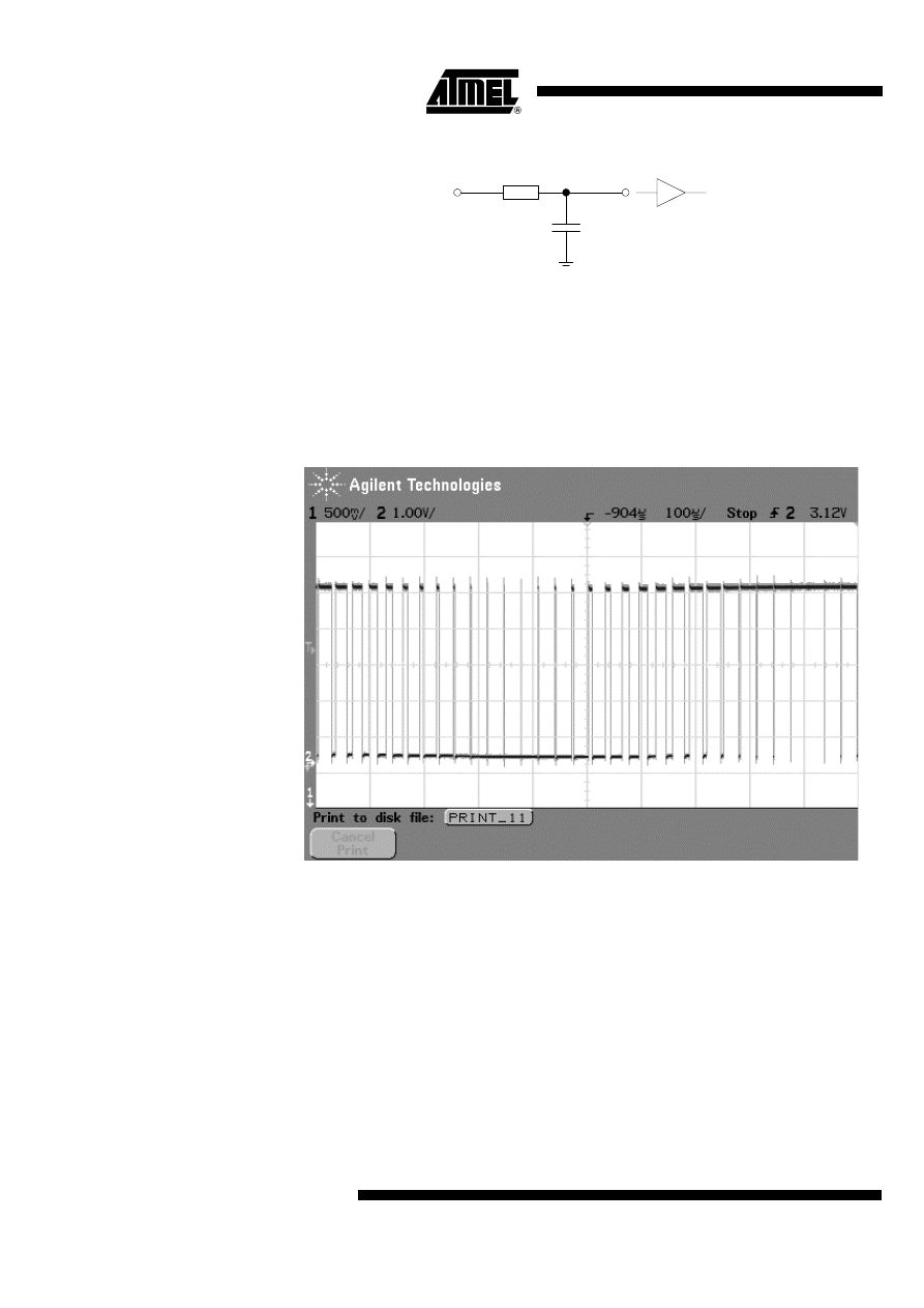
A real-life example of varying duty cycle – Pulse Width Modulation – is shown in figure
2.
Figure 2. PWM Output with Varying Duty Cycle
In the AVR, the timer/counters are used to generate PWM signals. To change the PWM
base frequency, the timer clock frequency and top counter value is changed. Faster
clock and/or lower top value will increase the PWM base frequency, or timer overflow
frequency. With full resolution (top value 255) the maximum PWM base frequency is
250 kHz. Increasing the base frequency beyond this frequency will be at the expense of
reduced resolution, since fewer step are then available from 0% to 100% duty cycle.
Altering the value of the Output Compare Registers (OCR) changes the duty cycle.
Increasing the OCR value increases the duty cycle. The PWM output is high until the
OCR value is reached, and low until the timer reaches the top value and wraps back to
0. This is called Fast-PWM mode.
PWM in
Analog out
R
C

3
AVR131 App Note
2542A–AVR–09/03
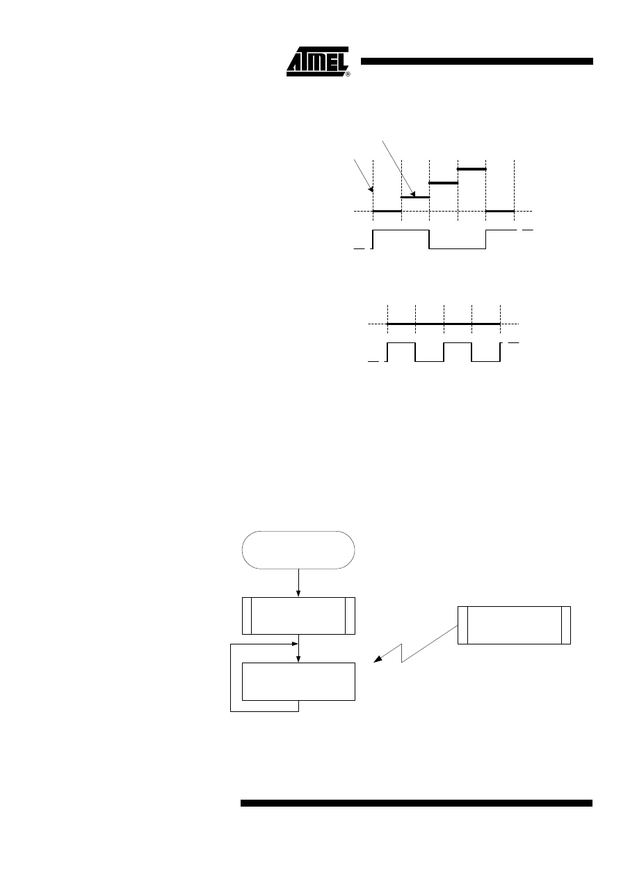
Figure 3. Counter Values and PWM Output
If using the high-speed PWM to generate analog signals, the step-size between the ana-
log levels is depending on the resolution of the PWM. The higher base frequency the
more easily is it to attenuate the base frequency and thereby minimize the signal ripple.
The selection of resolution versus base frequency is thus an application dependent
trade-off.
Alternative Usage
The high-speed timer can also be used to generate high frequency digital signals, which
can be used to clock other digital parts in the application. Setting the counter top value
to a small value, very high base frequencies are available.
The highest possible timer clock frequency for the ATtiny26 high-speed timer is 64 MHz
(no prescaling). At 16 MHz PWM base frequency (top value 3) the OCR value can be
set to 0, 1 (25% duty cycle), 2 (50% duty cycle, A in Figure 4) or 3 (100% duty cycle).
This shows that lowering the top value to increase the PWM base frequency reduces
the resolution.
To achieve the maximum output frequency from the timer, it must be run in non-PWM
mode. Both the OCR value and the top value must be set to 0. The counter is then stuck
at 0. Setting the Output Compare Match action to “toggle output” makes the timer toggle
the output on every timer clock tick. The result is a 32 MHz signal (B in Figure 4).
OCR value
Counter value
PWM output

4
AVR131 App Note
2542A–AVR–09/03
Figure 4. High Frequency Digital Output
Application Example
Figure 5 illustrates how to generate a sine wave from the high-speed PWM output.
The code consists of 3 parts: Initialization, Timer1 overflow interrupt service routine and
a sleep loop. The implementation assumes that the device system clock is 8 MHz.
Figure 5. Main Loop of Sine Wave Generator Example Code
TOP
OCR
TOP
OCR
TOP
OCR
TOP
OCR
OCR
TOP
64 MHz timer clock ticks
16 MHz 50% PWM
32 MHz non-PWM mode
Counter values
(A)
(B)
Main( )
Init()
Sleep
Timer1 OVF interrupt

5
AVR131 App Note
2542A–AVR–09/03
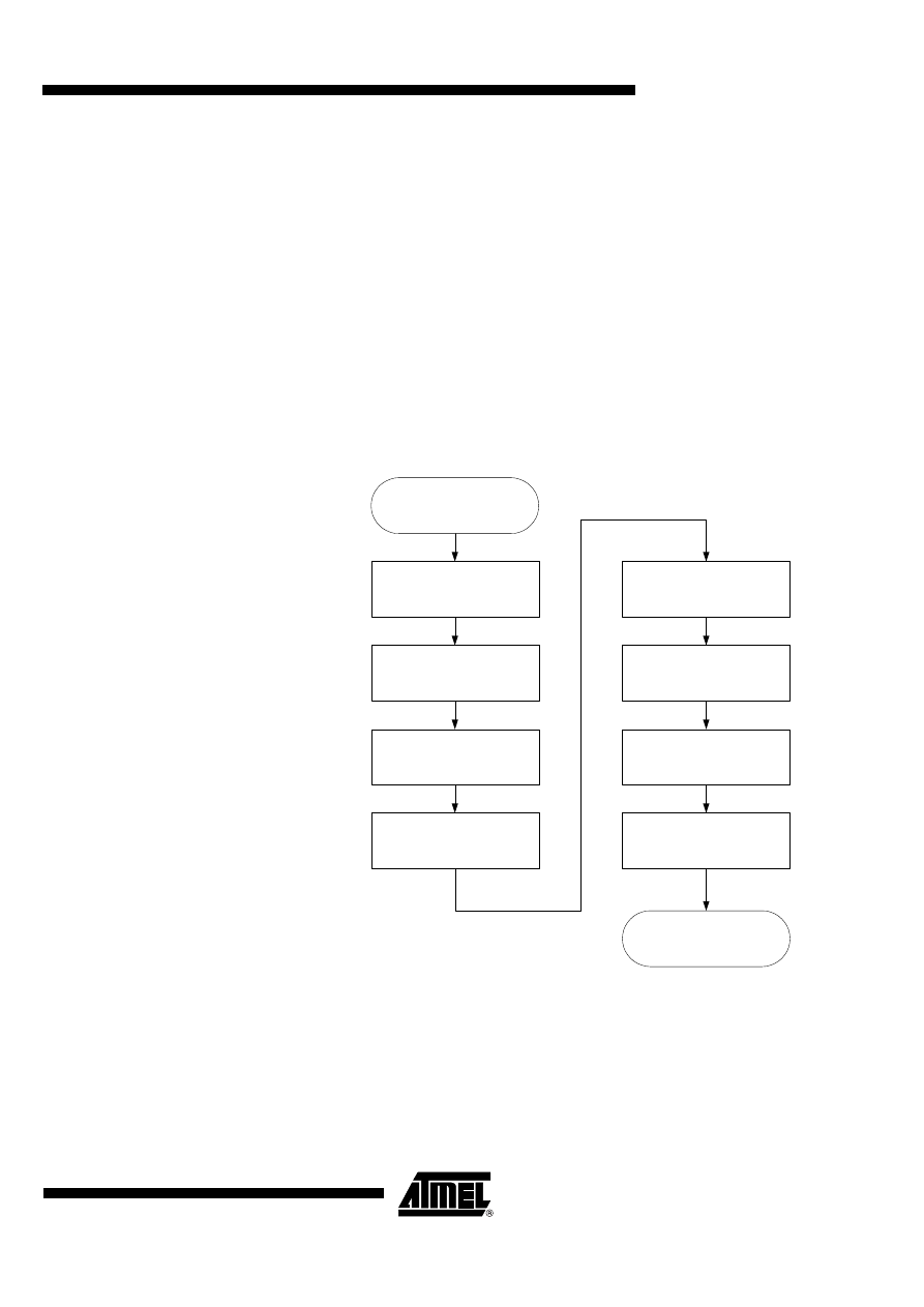
Initialization
To be able to generate an output from the PWM, the Output Compare Pin of Timer1
(OC1A) is set up as output.
Next the Timer1 is set up: The clock source for the timer is prepared – the PLL is started
and locked to the system clock (required). The PLL takes approximately 100 ms to lock
onto the system clock and it is therefore necessary to wait for the PLL lock flag before
proceeding. Once the PLL is locked it is selected as clock source for the timer.
The PWM mode is then selected so that the OC1A pin toggles on compare match and
the Top value of the timer is set to 0xFF. The Top value affects the resolution and the
base frequency of the PWM – the higher the Top value is the higher resolution and the
lower base frequency.
The Timer is now ready to be started: The prescaler is set, which also starts the timer.
Finally, the Overflow interrupt is enabled.
Figure 6. Init Routine, Initializes Pin and Timer1 to Operate in Fast PWM Mode
Interrupt Service Routine
When the Timer1 value reaches the OCR1C value (0xFF), the Timer Overflow interrupt
service routine (ISR) is executed. This happens at a constant interval, since OCR1C is
constant. This interval is the base frequency of the fast PWM output signal.
In the Timer1 Overflow ISR, a look up in a sine table is made. On each look-up the index
to the look-up table is incremented so that new values can be loaded. The value from
the sine table is written to OCR1A. In this way the pulse width is modulated to the sine
Init()
Set PB1 as output
Enable and lock PLL
Wait for PLL to lock
(app. 100 ms)
Set PLL as PWM clock
source
Set PWM mode: toggle
OC1A on compare
Set PWM Top value:
OCR1C = 0xFF
Enable Timer/ Set PWM
clock prescaler to PCK/2
(32 MHz PWM clock)
Return
Enable Timer1 OVF
interrupt

6
AVR131 App Note
2542A–AVR–09/03
wave. Note that the OCR1A register is buffered and that the latching of the buffer into
the actual OCR1A register takes place on the timer overflow.
The interrupt routine takes 13 clock cycles to execute. The call and return to and from
the interrupt comes in addition – in total 21 system clock cycles. Since Timer1 is an 8-bit
timer the interrupt occurs every 256/(PWM_clock/system_clock) cycle. The example is
based on that the device is clocked from the internal RC oscillator, which is 8 MHz. If the
maximum PWM clock, 64 MHz, is used this would mean a Timer1 Overflow interrupt
every 32 cycles.
Though it is possible to clock the PWM with the maximum frequency of 64 MHz, the
PWM clock is in this application note prescaled by 4 to 16 MHz to illustrate the use of
the prescaler.
Figure 7. Timer1 Overflow Interrupt Service Routine
Idle
The sleep mode “Idle” is used to put the device into power reduction state while waiting
for the Interrupt to occur. When the interrupt is serviced, it goes back to sleep.
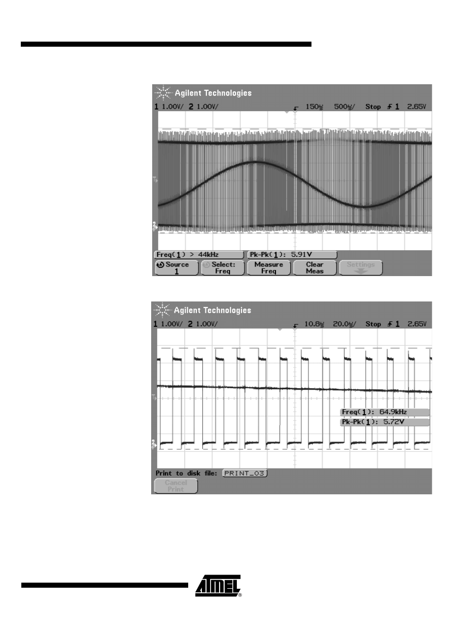
Scope Pictures
The following scope pictures are examples of sine wave signals generated by the
ATtiny26 PWM. The scope snap-shots show the output on the OC1A pin, which is the
digital pulse modulated signal, and the filtered/shaped PWM signal. A simple RC filter is
used to shape the PWM signal to a sine wave – an analog signal where the amplitude is
given by the duty cycle of the PWM output. The RC filter used has an R = 10 k
Ω
and a
C = 100 nF, resulting in a filter crossover frequency of 1 kHz, which will let the low fre-
quency sine wave pass while filtering out the high frequency PWM base.
Timer1 OVF ISR
Look-up new pulse width in
sine table
Increment sine table pointer
Copy sine value (pulse
width) to OCR1A
Return from interrupt

7
AVR131 App Note
2542A–AVR–09/03
Figure 8. OC1A Output – Filtered and Not Filtered
Figure 9. OC1A Output – Filtered and Not Filtered, Details

Printed on recycled paper.
Disclaimer: Atmel Corporation makes no warranty for the use of its products, other than those expressly contained in the Company’s standard
warranty which is detailed in Atmel’s Terms and Conditions located on the Company’s web site. The Company assumes no responsibility for any
errors which may appear in this document, reserves the right to change devices or specifications detailed herein at any time without notice, and
does not make any commitment to update the information contained herein. No licenses to patents or other intellectual property of Atmel are
granted by the Company in connection with the sale of Atmel products, expressly or by implication. Atmel’s products are not authorized for use
as critical components in life support devices or systems.
Atmel Corporation
Atmel Operations
2325 Orchard Parkway
San Jose, CA 95131, USA
Tel: 1(408) 441-0311
Fax: 1(408) 487-2600
Regional Headquarters
Europe
Atmel Sarl
Route des Arsenaux 41
Case Postale 80
CH-1705 Fribourg
Switzerland
Tel: (41) 26-426-5555
Fax: (41) 26-426-5500
Asia
Room 1219
Chinachem Golden Plaza
77 Mody Road Tsimshatsui
East Kowloon
Hong Kong
Tel: (852) 2721-9778
Fax: (852) 2722-1369
Japan
9F, Tonetsu Shinkawa Bldg.
1-24-8 Shinkawa
Chuo-ku, Tokyo 104-0033
Japan
Tel: (81) 3-3523-3551
Fax: (81) 3-3523-7581
Memory
2325 Orchard Parkway
San Jose, CA 95131, USA
Tel: 1(408) 441-0311
Fax: 1(408) 436-4314
Microcontrollers
2325 Orchard Parkway
San Jose, CA 95131, USA
Tel: 1(408) 441-0311
Fax: 1(408) 436-4314
La Chantrerie
BP 70602
44306 Nantes Cedex 3, France
Tel: (33) 2-40-18-18-18
Fax: (33) 2-40-18-19-60
ASIC/ASSP/Smart Cards
Zone Industrielle
13106 Rousset Cedex, France
Tel: (33) 4-42-53-60-00
Fax: (33) 4-42-53-60-01
1150 East Cheyenne Mtn. Blvd.
Colorado Springs, CO 80906, USA
Tel: 1(719) 576-3300
Fax: 1(719) 540-1759
Scottish Enterprise Technology Park
Maxwell Building
East Kilbride G75 0QR, Scotland
Tel: (44) 1355-803-000
Fax: (44) 1355-242-743
RF/Automotive
Theresienstrasse 2
Postfach 3535
74025 Heilbronn, Germany
Tel: (49) 71-31-67-0
Fax: (49) 71-31-67-2340
1150 East Cheyenne Mtn. Blvd.
Colorado Springs, CO 80906, USA
Tel: 1(719) 576-3300
Fax: 1(719) 540-1759
Biometrics/Imaging/Hi-Rel MPU/
High Speed Converters/RF Datacom
Avenue de Rochepleine
BP 123
38521 Saint-Egreve Cedex, France
Tel: (33) 4-76-58-30-00
Fax: (33) 4-76-58-34-80
Literature Requests
www.atmel.com/literature
2542A–AVR–09/03
© Atmel Corporation 2003. All rights reserved. Atmel
®
and combinations thereof, and AVR
®
are the registered trademarks of Atmel Corpora-
tion or its subsidiaries. Other terms and product names may be the trademarks of others.
Document Outline
Wyszukiwarka
Podobne podstrony:
A ZVS PWM Inverter With Active Voltage Clamping Using the Reverse Recovery Energy of the Diodes
87 1237 1248 Machinability and Tool Wear During the High Speed Milling of Some Hardened
Fast virus detection by using high speed time delay neural networks
An investigation of shock induced temperature rise and melting of bismuth using high speed optical p
CAN on the AVR
11 3 4 6 Lab Using the CLI to Gather Network?vice Information
DUI0379C using the assembler
antybiotyki High Speed Countercurrent
Roszak, Rewers, Pliszka USING THE 3D
high speed usb pcb layout recom Nieznany
ADSL High Speed Internetzugang
Fotopolis pl High speed photography w warunkach domowych
Barron Using the standard on objective measures for concert auditoria, ISO 3382, to give reliable r
11 3 4 6 Lab Using the CLI to Gather Network (2)
Using the PSpice Library Translator
High Speed Countercurrent Chromatography
Developing your STM32VLDISCOVERY application using the MDK ARM
więcej podobnych podstron