2
3
4
5
6
7
8
SERIAL
DATA OUT
SERIAL
DATA IN
OUTPUT
ENABLE
LOGIC
SUPPLY
STROBE
LOGIC
GROUND
CLOCK
CLK
V
ST
OE
DD
1
SUB
POWER
GROUND
SHIFT REGISTER
LATCHES
9
10
11
12
13
14
15
16
OUT
1
OUT
2
OUT
3
Dwg. PP-026A
OUT
8
OUT
7
OUT
6
OUT
5
OUT
4
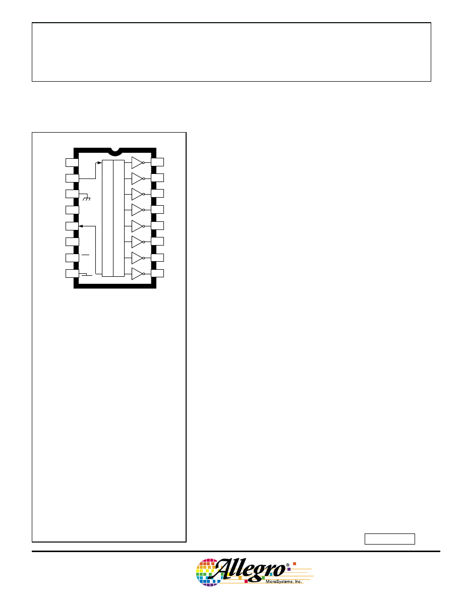
BiMOS II 8-BIT SERIAL-INPUT,
LATCHED DRIVERS
Always order by complete part number, e.g., UCN5821A .
Data Sheet
26185.12E
5821
AND
5822
Note the DIP package and the SOIC package are
electrically identical and share common terminal
number assignments.
A merged combination of bipolar and MOS technology gives
these devices an interface flexibility beyond the reach of standard
logic buffers and power driver arrays. The UCN5821A,
UCN5821LW, UCN5822A, and UCN5822LW each have an
eight-bit CMOS shift register and CMOS control circuitry, eight
CMOS data latches, and eight bipolar current-sinking Darlington
output drivers. The UCN5821A/LW and UCN5822A/LW are
identical except for rated output voltage.
BiMOS II devices have much higher data-input rates than the
original BiMOS circuits. With a 5 V logic supply, they will
typically operate at better than 5 MHz. With a 12 V supply,
significantly higher speeds are obtained. The CMOS inputs are
compatible with standard CMOS and NMOS logic levels. TTL
circuits may require the use of appropriate pull-up resistors. By
using the serial data output, the drivers can be cascaded for
interface applications requiring additional drive lines.
The UCN5821/22A are furnished in a standard 16-pin plastic
DIP; the UCN5821/22LW are in a 16-lead wide-body SOIC for
surface-mount applications. The UCN5821A is also available for
operation from -40
°C to +85°C. To order, change the prefix from
‘UCN’ to ‘UCQ’.
FEATURES
■ To 3.3 MHz Data Input Rate
■ CMOS, NMOS, TTL Compatible
■ Internal Pull-Down Resistors
■ Low-Power CMOS Logic & Latches
■ High-Voltage Current-Sink Outputs
■ Automotive Capable
ABSOLUTE MAXIMUM RATINGS
at 25
°
C Free-Air Temperature
Output Voltage, V
OUT
UCN5821A & UCN5821LW ..... 50 V
UCN5822A & UCN5822LW ..... 80 V
Logic Supply Voltage, V
DD
............. 15 V
Input Voltage Range,
V
IN
.................. -0.3 V to V
DD
+ 0.3 V
Continuous Output Current,
I
OUT
..................................... 500 mA
Package Power Dissipation, P
D
Package Code ‘A’ .................. 2.1 W
Package Code ‘LW’ ............... 1.5 W
Operating Temperature Range,
T
A
............................ -20
°
C to +85
°
C
Storage Temperature Range,
T
S
.......................... -55
°
C to +150
°
C
Caution: CMOS devices have input static protection
but are susceptible to damage when exposed to
extremely high static electrical charges.
www.allegromicro.com
5821
AND
5822
8-BIT SERIAL-INPUT,
LATCHED DRIVERS
115 Northeast Cutoff, Box 15036
Worcester, Massachusetts 01615-0036 (508) 853-5000
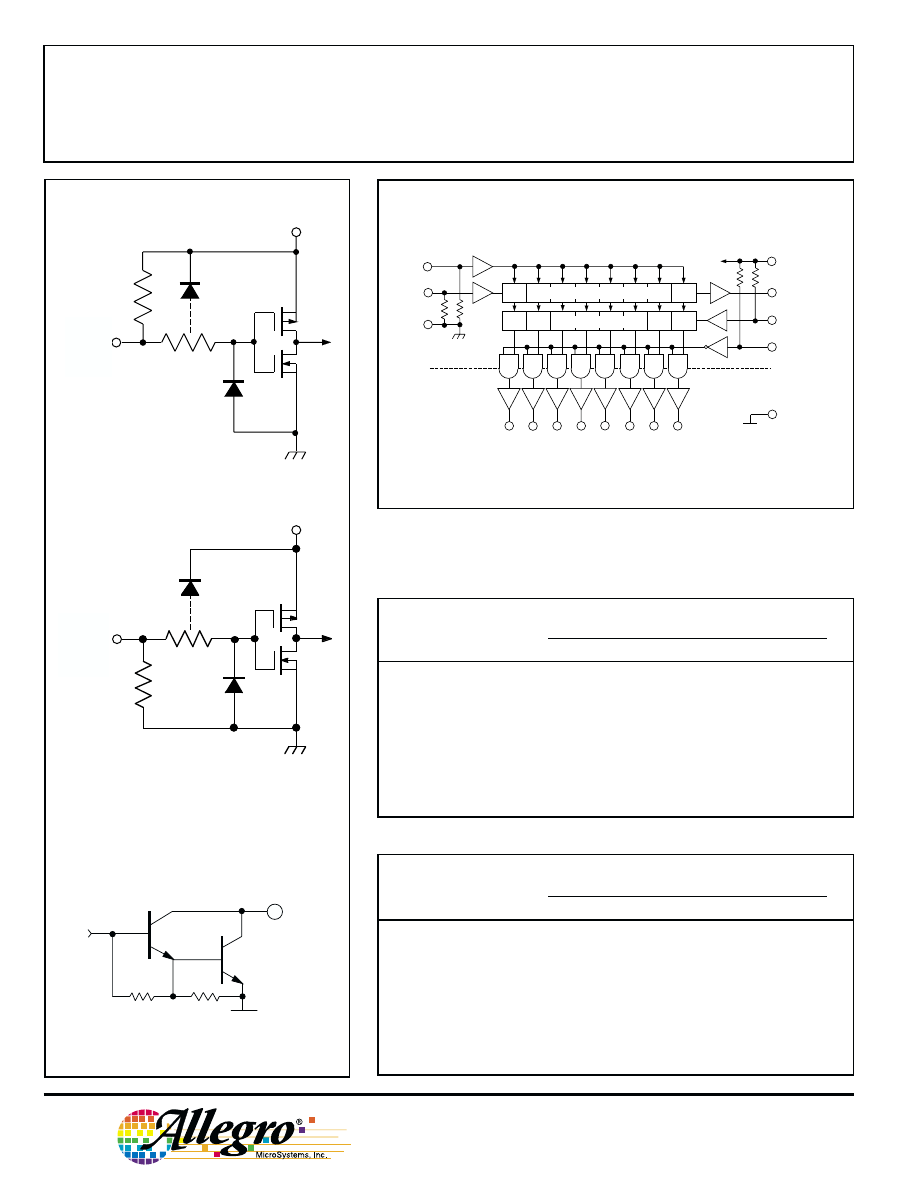
MOS
BIPOLAR
OUT
1
OUT
2
LOGIC
GROUND
STROBE
OUTPUT ENABLE
(ACTIVE LOW)
SERIAL
DATA OUT
5
7
6
Dwg. FP-013A
OUT
3
CLOCK
SERIAL
DATA IN
SERIAL-PARALLEL SHIFT REGISTER
LATCHES
V
DD
LOGIC
SUPPLY
1
2
3
16
OUT
6
OUT
7
OUT
8
15
14
11
10
9
OUT
4
OUT
5
13
12
8
4
POWER
GROUND
SUB
FUNCTIONAL BLOCK DIAGRAM
TYPICAL INPUT CIRCUITS
Dwg. No. A-14,314
Dwg. EP-010-3
IN
V
DD
Dwg. EP-010-4A
IN
V
DD
STROBE &
OUTPUT
ENABLE
CLOCK &
SERIAL
DATA IN
Copyright © 1985, 2000, Allegro MicroSystems, Inc.
Number of Outputs ON
UCN5821A Max. Allowable Duty Cycle
(I
OUT
= 200 mA
at Ambient Temperature of
V
DD
= 12 V)
25
°
C
40
°
C
50
°
C
60
°
C
70
°
C
8
90%
79%
72%
65%
57%
7
100%
90%
82%
74%
65%
6
100%
100%
96%
86%
76%
5
100%
100%
100%
100%
91%
4
100%
100%
100%
100%
100%
3
100%
100%
100%
100%
100%
2
100%
100%
100%
100%
100%
1
100%
100%
100%
100%
100%
Number of Outputs ON
UCN5821LW Max. Allowable Duty Cycle
(I
OUT
= 200 mA
at Ambient Temperature of
V
DD
= 12 V)
25
°
C
40
°
C
50
°
C
60
°
C
70
°
C
8
67%
59%
54%
49%
43%
7
77%
68%
62%
56%
49%
6
90%
79%
72%
65%
57%
5
100%
95%
86%
78%
68%
4
100%
100%
100%
98%
86%
3
100%
100%
100%
100%
100%
2
100%
100%
100%
100%
100%
1
100%
100%
100%
100%
100%
TYPICAL OUTPUT DRIVER
OUT
SUB
7.2K
3K
NOTE — There is an indeterminate resistance between logic ground and power
ground. For proper operation, these terminals must be externally connected
together.
5821
AND
5822
8-BIT SERIAL-INPUT,
LATCHED DRIVERS
www.allegromicro.com
Limits
Characteristic
Symbol
Test Conditions
Min.
Max.
Units
Output Leakage
I
CEX
UCN5821A/LW, V
OUT
= 50 V
—
50
µA
Current
UCN5822A/LW, V
OUT
= 80 V
—
50
µA
UCN5821A/LW, V
OUT
= 50 V, T
A
= +70
°C
—
100
µA
UCN5822A/LW, V
OUT
= 80 V, T
A
= +70
°C
—
100
µA
Collector-Emitter
V
CE(SAT)
I
OUT
= 100 mA
—
1.1
V
Saturation Voltage
I
OUT
= 200 mA
—
1.3
V
I
OUT
= 350 mA, V
DD
= 7.0 V
—
1.6
V
Input Voltage
V
IN(0)
—
0.8
V
V
IN(1)
V
DD
= 12 V
10.5
—
V
V
DD
= 5.0 V
3.5
—
V
Input Resistance
r
IN
V
DD
= 12 V
50
—
k
Ω
V
DD
= 5.0 V
50
—
k
Ω
Supply Current
I
DD(ON)
One Driver ON, V
DD
= 12 V
—
4.5
mA
One Driver ON, V
DD
= 10 V
—
3.9
mA
One Driver ON, V
DD
= 5.0 V
—
2.4
mA
I
DD(OFF)
V
DD
= 5.0 V, All Drivers OFF, All Inputs = 0 V
—
1.6
mA
V
DD
= 12 V, All Drivers OFF, All Inputs = 0 V
—
2.9
mA
ELECTRICAL CHARACTERISTICS at T
A
= +25
°
C, V
DD
= 5 V, (unless otherwise specified).
5821
AND
5822
8-BIT SERIAL-INPUT,
LATCHED DRIVERS
115 Northeast Cutoff, Box 15036
Worcester, Massachusetts 01615-0036 (508) 853-5000
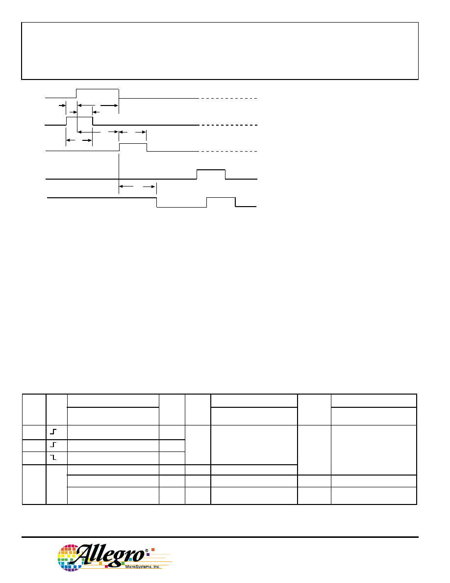
TIMING CONDITIONS
(V
DD
= 5.0 V, T
A
= +25
°
C, Logic Levels are V
DD
and Ground)
A.
Minimum Data Active Time Before Clock Pulse
(Data Set-Up Time) ....................................................................... 75 ns
B.
Minimum Data Active Time After Clock Pulse
(Data Hold Time) ........................................................................... 75 ns
C.
Minimum Data Pulse Width .............................................................. 150 ns
D.
Minimum Clock Pulse Width ............................................................ 150 ns
E.
Minimum Time Between Clock Activation and Strobe ....................... 30 ns
F.
Minimum Strobe Pulse Width ........................................................... 100 ns
G.
Typical Time Between Strobe Activation and
Output Transition .......................................................................... 1.0
µ
s
TRUTH TABLE
Serial
Shift Register Contents
Serial
Latch Contents
Output Contents
Data
Clock
Data
Strobe
Output
Input
Input I
1
I
2
I
3
.............. I
8
Output
Input
I
1
I
2
I
3
.............. I
8
Enable
I
1
I
2
I
3
.............. I
8
H
H
R
1
R
2
.............. R
7
R
7
L
L
R
1
R
2
.............. R
7
R
7
X
R
1
R
2
R
3
.............. R
8
R
8
X
X
X
.............. X
X
L
R
1
R
2
R
3
.............. R
8
P
1
P
2
P
3
.............. P
8
P
8
H
P
1
P
2
P
3
.............. P
8
L
P
1
P
2
P
3
.............. P
8
X
X
X
.............. X
H
H
H
H
.............. H
L = Low Logic Level H = High Logic Level X = Irrelevant P = Present State R = Previous State
Dwg. No. A-12,627
Serial Data present at the input is
transferred to the shift register on the
logic “0” to logic “1” transition of the
CLOCK input pulse. On succeeding
CLOCK pulses, the registers shift data
information towards the SERIAL DATA
OUTPUT. The SERIAL DATA must
appear at the input prior to the rising edge
of the CLOCK input waveform.
Information present at any register is
transferred to its respective latch when the
STROBE is high (serial-to-parallel con-
version). The latches will continue to
accept new data as long as the STROBE
is held high. Applications where the
latches are bypassed (STROBE tied high)
will require that the ENABLE input be
high during serial data entry.
When the ENABLE input is high, all
of the output buffers are disabled (OFF)
without affecting the information stored
in the latches or shift register. With the
ENABLE input low, the outputs are
controlled by the state of the latches.
A
D
B
C
E
F
CLOCK
DATA IN
STROBE
OUTPUT
ENABLE
OUT
N
G
5821
AND
5822
8-BIT SERIAL-INPUT,
LATCHED DRIVERS
www.allegromicro.com
NOTES: 1. Lead thickness is measured at seating plane or below.
2. Lead spacing tolerance is non-cumulative.
3. Exact body and lead configuration at vendor’s option within limits shown.
0.014
0.008
0.300
BSC
Dwg. MA-001-16A in
0.430
MAX
16
1
8
0.280
0.240
0.210
MAX
0.070
0.045
0.015
MIN
0.022
0.014
0.100
BSC
0.005
MIN
0.150
0.115
9
0.775
0.735
0.355
0.204
7.62
BSC
Dwg. MA-001-16A mm
10.92
MAX
16
1
8
7.11
6.10
5.33
MAX
1.77
1.15
0.39
MIN
0.558
0.356
2.54
BSC
0.13
MIN
3.81
2.93
9
19.68
18.67
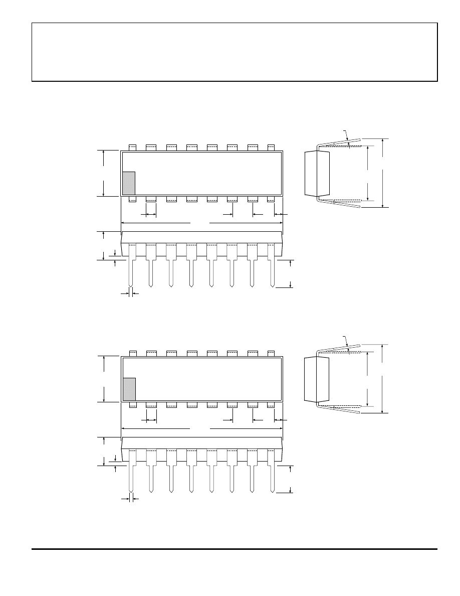
UCN5821A and UCN5822A
Dimensions in Inches
(controlling dimensions)
Dimensions in Millimeters
(for reference only)
5821
AND
5822
8-BIT SERIAL-INPUT,
LATCHED DRIVERS
115 Northeast Cutoff, Box 15036
Worcester, Massachusetts 01615-0036 (508) 853-5000
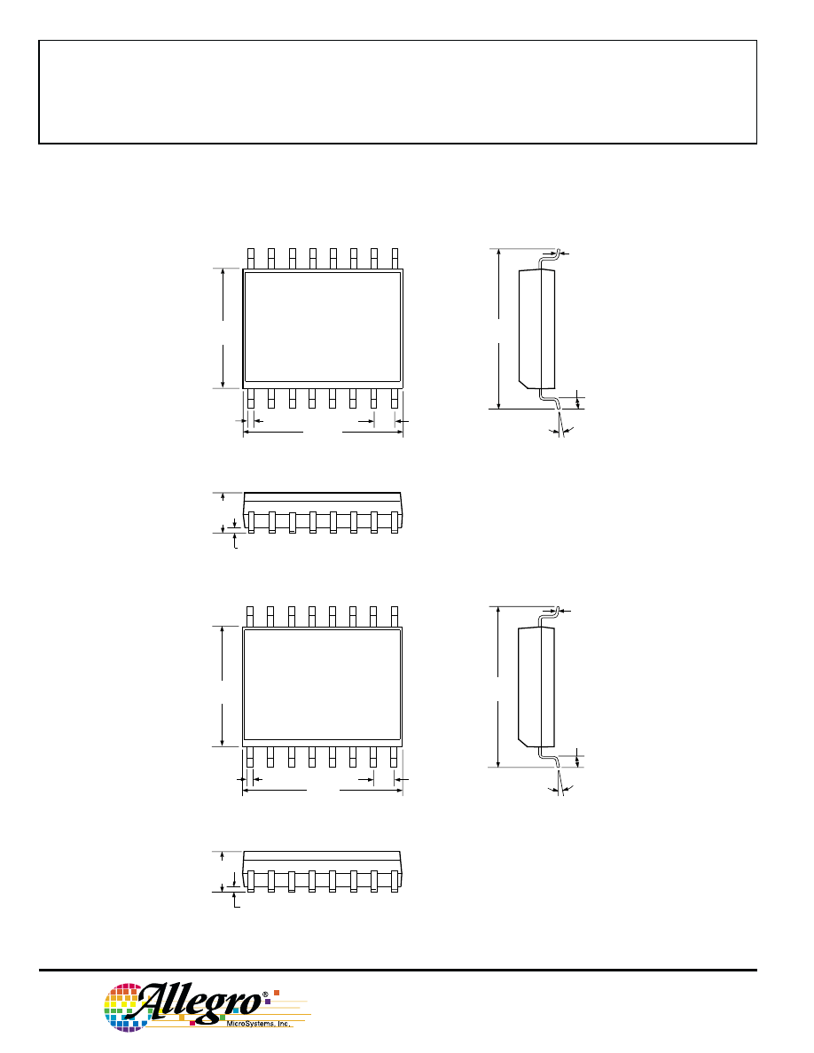
NOTES: 1. Lead spacing tolerance is non-cumulative.
2. Exact body and lead configuration at vendor’s option within limits shown.
UCN5821LW and UCN5822LW
Dimensions in Inches
(for reference only)
Dimensions in Millimeters
(controlling dimensions)
1
2
3
0.2992
0.2914
0.4133
0.3977
0.419
0.394
0.020
0.013
0.0926
0.1043
0.0040
MIN.
0.0125
0.0091
0.050
0.016
0
°
TO
8
°
Dwg. MA-008-16A in
0.050
BSC
16
9
9
16
1
2
3
7.60
7.40
10.50
10.10
10.65
10.00
0.51
0.33
2.65
2.35
0.10
MIN.
0.32
0.23
1.27
0.40
0
°
TO
8
°
Dwg. MA-008-16A mm
1.27
BSC

5821
AND
5822
8-BIT SERIAL-INPUT,
LATCHED DRIVERS
www.allegromicro.com
The products described here are manufactured under one or more
U.S. patents or U.S. patents pending.
Allegro MicroSystems, Inc. reserves the right to make, from time to
time, such departures from the detail specifications as may be
required to permit improvements in the performance, reliability, or
manufacturability of its products. Before placing an order, the user is
cautioned to verify that the information being relied upon is current.
Allegro products are not authorized for use as critical components
in life-support devices or systems without express written approval.
The information included herein is believed to be accurate and
reliable. However, Allegro MicroSystems, Inc. assumes no responsi-
bility for its use; nor for any infringement of patents or other rights of
third parties which may result from its use.
5821
AND
5822
8-BIT SERIAL-INPUT,
LATCHED DRIVERS
115 Northeast Cutoff, Box 15036
Worcester, Massachusetts 01615-0036 (508) 853-5000
POWER
INTERFACE DRIVERS
Function
Output Ratings*
Part Number†
SERIAL-INPUT LATCHED DRIVERS
8-Bit (saturated drivers)
-120 mA
50 V‡
5895
8-Bit
350 mA
50 V5821
8-Bit
350 mA
80 V5822
8-Bit
350 mA
50 V‡
5841
8-Bit
350 mA
80 V‡
5842
8-Bit (constant-current LED driver)
75 mA
17 V6275
8-Bit (DMOS drivers)
250 mA
50 V6595
8-Bit (DMOS drivers)
350 mA
50 V‡
6A595
8-Bit (DMOS drivers)
100 mA
50 V6B595
10-Bit (active pull-downs)
-25 mA
60 V5810-F and 6809/10
12-Bit (active pull-downs)
-25 mA
60 V5811 and 6811
16-Bit (constant-current LED driver)
75 mA
17 V6276
20-Bit (active pull-downs)
-25 mA
60 V5812-F and 6812
32-Bit (active pull-downs)
-25 mA
60 V5818-F and 6818
32-Bit
100 mA
30 V5833
32-Bit (saturated drivers)
100 mA
40 V5832
PARALLEL-INPUT LATCHED DRIVERS
4-Bit
350 mA
50 V‡
5800
8-Bit
-25 mA
60 V5815
8-Bit
350 mA
50 V‡
5801
8-Bit (DMOS drivers)
100 mA
50 V6B273
8-Bit (DMOS drivers)
250 mA
50 V6273
SPECIAL-PURPOSE DEVICES
Unipolar Stepper Motor Translator/Driver
1.25 A
50 V‡
5804
Addressable 8-Bit Decoder/DMOS Driver
250 mA
50 V6259
Addressable 8-Bit Decoder/DMOS Driver
350 mA
50 V‡
6A259
Addressable 8-Bit Decoder/DMOS Driver
100 mA
50 V6B259
Addressable 28-Line Decoder/Driver
450 mA
30 V6817
*
Current is maximum specified test condition, voltage is maximum rating. See specification for sustaining voltage limits.
Negative current is defined as coming out of (sourcing) the output.
†
Complete part number includes additional characters to indicate operating temperature range and package style.
‡
Internal transient-suppression diodes included for inductive-load protection.
Wyszukiwarka
Podobne podstrony:
5821
5821
5821
5821
5821
[Free scores[1] com] gitlitz paul waiting for the power 5821
więcej podobnych podstron