©
Semiconductor Components Industries, LLC, 2006
January, 2006 − Rev. 3
1
Publication Order Number:
BC327/D
BC327, BC327−16,
BC327−25, BC327−40
Amplifier Transistors
PNP Silicon
Features
•
Pb−Free Packages are Available*
MAXIMUM RATINGS
Rating
Symbol
Value
Unit
Collector −Emitter Voltage
V
CEO
−45
Vdc
Collector −Base Voltage
V
CES
−50
Vdc
Collector −Emitter Voltage
V
EBO
−5.0
Vdc
Collector Current − Continuous
I
C
−800
mAdc
Total Power Dissipation @ T
A
= 25
°
C
Derate above T
A
= 25
°
C
P
D
625
5.0
mW
mW/
°
C
Total Power Dissipation @ T
A
= 25
°
C
Derate above T
A
= 25
°
C
P
D
1.5
12
W
mW/
°
C
Operating and Storage Junction
Temperature Range
T
J
, T
stg
−55 to +150
°
C
THERMAL CHARACTERISTICS
Characteristic
Symbol
Max
Unit
Thermal Resistance, Junction−to−Ambient
R
q
JA
200
°
C/W
Thermal Resistance, Junction−to−Case
R
q
JC
83.3
°
C/W
Maximum ratings are those values beyond which device damage can occur.
Maximum ratings applied to the device are individual stress limit values (not
normal operating conditions) and are not valid simultaneously. If these limits are
exceeded, device functional operation is not implied, damage may occur and
reliability may be affected.
*For additional information on our Pb−Free strategy and soldering details, please
download the ON Semiconductor Soldering and Mounting Techniques
Reference Manual, SOLDERRM/D.
BCxx = Device Code
A
= Assembly Location
Y
= Year
WW
= Work Week
G
= Pb−Free Package
MARKING DIAGRAM
TO−92
CASE 29
STYLE 17
1 2
3
(Note: Microdot may be in either location)
http://onsemi.com
BC
xx
AYWW
G
G
COLLECTOR
1
2
BASE
3
EMITTER
See detailed ordering, marking, and shipping information in
the package dimensions section on page 4 of this data sheet.
ORDERING INFORMATION
BC327, BC327−16, BC327−25, BC327−40
http://onsemi.com
2
ELECTRICAL CHARACTERISTICS
(T
A
= 25
°
C unless otherwise noted)
Characteristic
Symbol
Min
Typ
Max
Unit
OFF CHARACTERISTICS
Collector −Emitter Breakdown Voltage
(I
C
= −10 mA, I
B
= 0)
V
(BR)CEO
−45
−
−
Vdc
Collector −Emitter Breakdown Voltage
(I
C
= −100
m
A, I
E
= 0)
V
(BR)CES
−50
−
−
Vdc
Emitter −Base Breakdown Voltage
(I
E
= −10
m
A, I
C
= 0)
V
(BR)EBO
−5.0
−
−
Vdc
Collector Cutoff Current
(V
CB
= −30 V, I
E
= 0)
I
CBO
−
−
−100
nAdc
Collector Cutoff Current
(V
CE
= −45 V, V
BE
= 0)
I
CES
−
−
−100
nAdc
Emitter Cutoff Current
(V
EB
= −4.0 V, I
C
= 0)
I
EBO
−
−
−100
nAdc
ON CHARACTERISTICS
DC Current Gain
(I
C
= −100 mA, V
CE
= −1.0 V)
BC327
BC327−16
BC327−25
BC327−40
(I
C
= −300 mA, V
CE
= −1.0 V)
h
FE
100
100
160
250
40
−
−
−
−
−
630
250
400
630
−
−
Base−Emitter On Voltage
(I
C
= −300 mA, V
CE
= −1.0 V)
V
BE(on)
−
−
−1.2
Vdc
Collector −Emitter Saturation Voltage
(I
C
= −500 mA, I
B
= −50 mA)
V
CE(sat)
−
−
−0.7
Vdc
SMALL−SIGNAL CHARACTERISTICS
Output Capacitance
(V
CB
= −10 V, I
E
= 0, f = 1.0 MHz)
C
ob
−
11
−
pF
Current −Gain − Bandwidth Product
(I
C
= −10 mA, V
CE
= −5.0 V, f = 100 MHz)
f
T
−
260
−
MHz
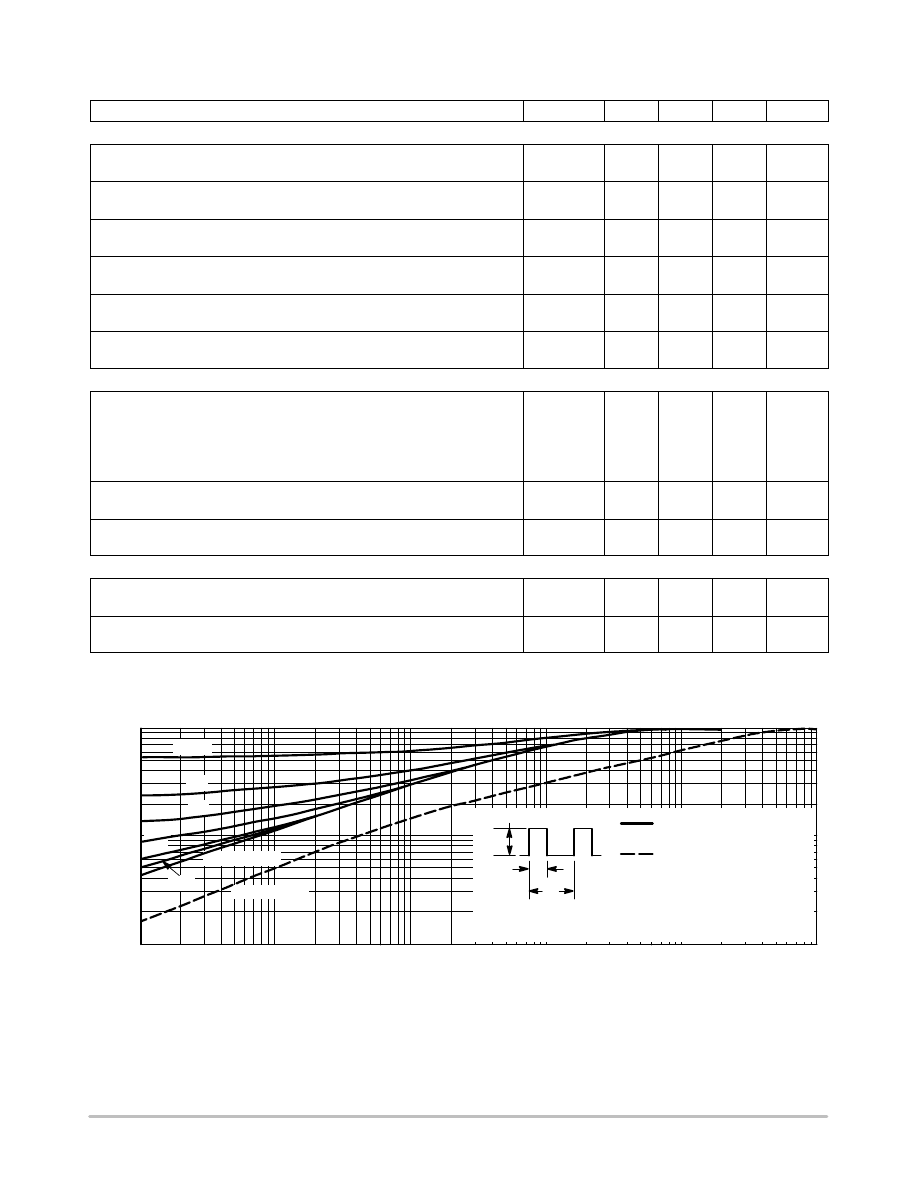
Figure 1. Thermal Response
t, TIME (SECONDS)
0.001 0.002
0.005
0.01
0.02
0.05
0.1
0.2
0.5
1.0
2.0
5.0
10
20
50
100
0.01
0.02
0.03
0.05
0.07
0.1
0.2
0.3
0.5
0.7
1.0
r(t)
, NORMALIZED EFFECTIVE
TRANSIENT
THERMAL
RESIST
ANCE
D = 0.5
0.2
0.1
0.05
0.02
0.01
SINGLE PULSE
q
JC
(t) = (t)
q
JC
q
JC
= 100
°
C/W MAX
q
JA
(t) = r(t)
q
JA
q
JA
= 375
°
C/W MAX
D CURVES APPLY FOR
POWER
PULSE TRAIN SHOWN
READ TIME AT t
1
T
J(pk)
− T
C
= P
(pk)
q
JC
(t)
t
1
t
2
P
(pk)
DUTY CYCLE, D = t
1
/t
2
SINGLE PULSE
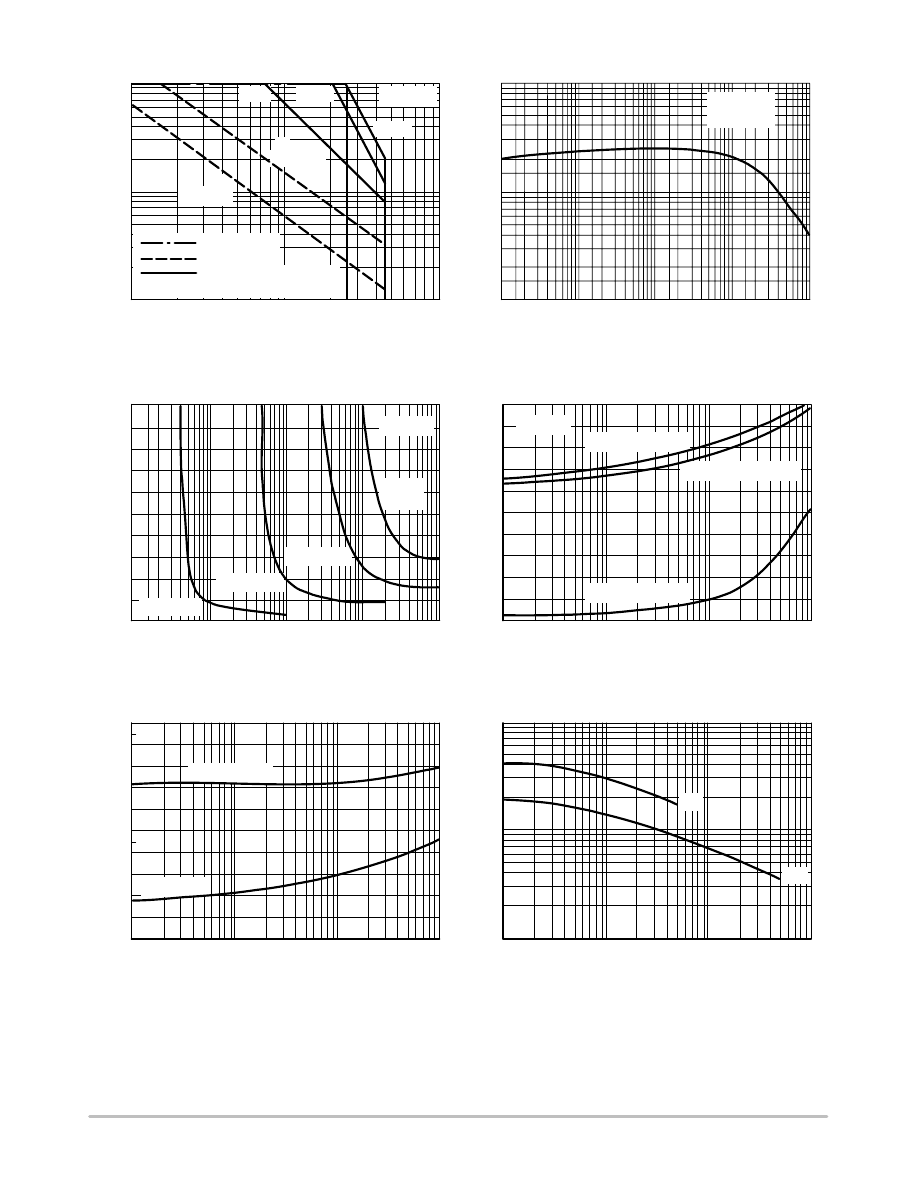
BC327, BC327−16, BC327−25, BC327−40
http://onsemi.com
3
−1000
−10
−100
−1.0
−3.0
−10
−30
V
CE
, COLLECTOR−EMITTER VOLTAGE
Figure 2. Active Region − Safe Operating Area
I
C
, COLLECTOR CURRENT (mA)
Figure 3. DC Current Gain
I C
, COLLECT
OR
CURRENT
(mA)
h FE
, DC CURRENT
GAIN
−100
1000
10
−1000
−0.1
−10
−100
100
−1.0
CURRENT LIMIT
THERMAL LIMIT
SECOND BREAKDOWN LIMIT
1.0 ms
1.0 s
T
J
= 135°C
100 ms
V
CE
= −1.0 V
T
A
= 25°C
T
A
= 25°C
T
C
= 25°C
dc
dc
(APPLIES BELOW RATED V
CEO
)
I
B
, BASE CURRENT (mA)
Figure 4. Saturation Region
I
C
, COLLECTOR CURRENT (mA)
Figure 5. “On” Voltages
100
10
1.0
V
R
, REVERSE VOLTAGE (VOLTS)
Figure 6. Temperature Coefficients
+1.0
I
C
, COLLECTOR CURRENT
Figure 7. Capacitances
−0.1
−1.0
−1.0
−10
−100
−1000
−2.0
−1.0
0
V CE
, COLLECT
OR−EMITTER
VOL
TAGE
(VOL
TS
V,
VOL
TAGE
(VOL
TS)
V,
TEMPERATURE COEFFICIENTS (mV/
C)°
θ
C, CAP
ACIT
ANCE
(pF)
−1.0
−0.8
−0.6
−0.4
−0.2
0
−0.01
−0.1
−10
−100
−1.0
−1.0
−0.8
−0.6
−0.4
−0.2
0
−1.0
−10
−1000
−100
−10
−100
T
J
= 25°C
I
C
= −10 mA
I
C
= −100 mA
I
C
= −300 mA
I
C
=
−500 mA
T
A
= 25°C
V
BE(sat)
@ I
C
/I
B
= 10
V
BE(on)
@ V
CE
= −1.0 V
V
CE(sat)
@ I
C
/I
B
= 10
q
VC
for V
CE(sat)
q
VB
for V
BE
C
ob
C
ib

BC327, BC327−16, BC327−25, BC327−40
http://onsemi.com
4
ORDERING INFORMATION
Device Order Number
Specific Device Marking
Package Type
Shipping
†
BC327
7
TO−92
5000 Units / Bulk
BC327G
7
TO−92
(Pb−Free)
5000 Units / Bulk
BC327RL1
327
TO−92
2000 / Tape & Reel
BC327RL1G
327
TO−92
(Pb−Free)
2000 / Tape & Reel
BC327ZL1
327
TO−92
2000 / Tape & Ammo Box
BC327ZL1G
327
TO−92
(Pb−Free)
2000 / Tape & Ammo Box
BC327−016
327
TO−92
5000 Units / Bulk
BC327−016G
327
TO−92
(Pb−Free)
5000 Units / Bulk
BC327−016ZL1
32716
TO−92
2000 / Tape & Ammo Box
BC327−016ZL1G
32716
TO−92
(Pb−Free)
2000 / Tape & Ammo Box
BC327−25RL1
7−25
TO−92
2000 / Tape & Reel
BC327−25RL1G
7−25
TO−92
(Pb−Free)
2000 / Tape & Reel
BC327−25ZL1
32725
TO−92
2000 / Tape & Ammo Box
BC327−25ZL1G
32725
TO−92
(Pb−Free)
2000 / Tape & Ammo Box
BC327−040
327
TO−92
2000 / Tape & Reel
BC327−040G
327
TO−92
(Pb−Free)
2000 / Tape & Reel
BC327−40ZL1
7−40
TO−92
2000 / Tape & Ammo Box
BC327−40ZL1G
7−40
TO−92
(Pb−Free)
2000 / Tape & Ammo Box
†For information on tape and reel specifications, including part orientation and tape sizes, please refer to our Tape and Reel Packaging
Specifications Brochure, BRD8011/D.
BC327, BC327−16, BC327−25, BC327−40
http://onsemi.com
5
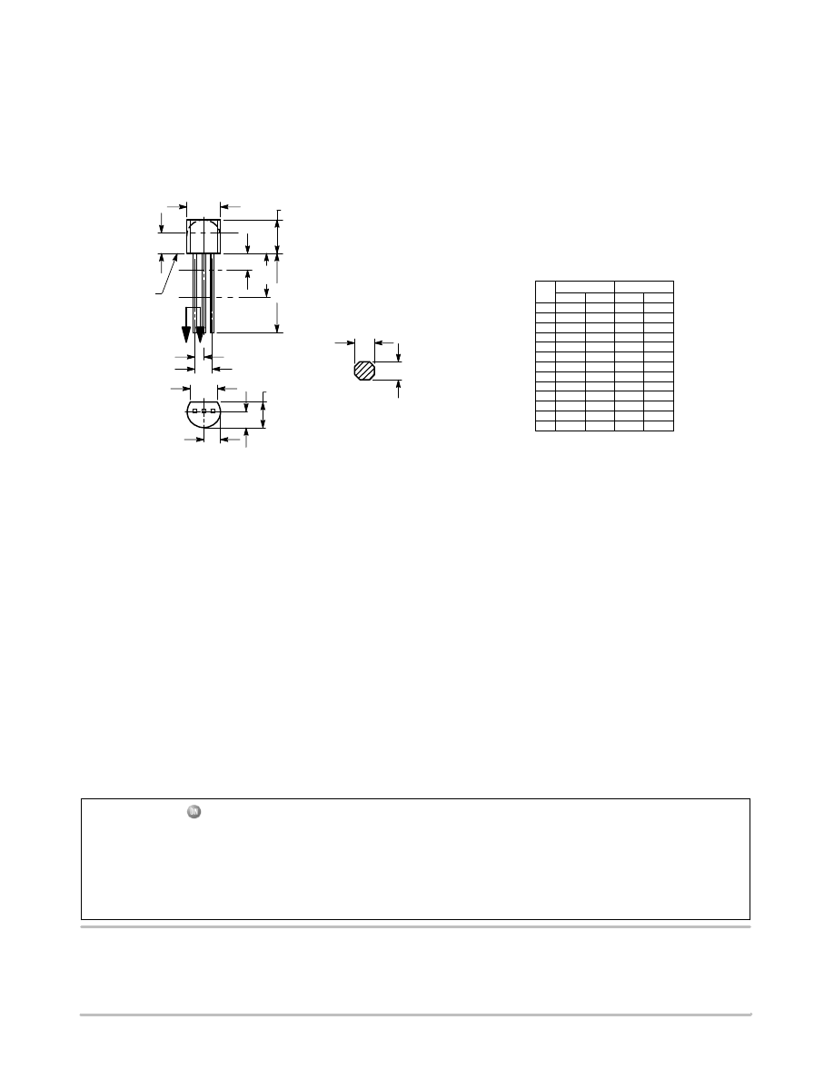
PACKAGE DIMENSIONS
NOTES:
1. DIMENSIONING AND TOLERANCING PER ANSI
Y14.5M, 1982.
2. CONTROLLING DIMENSION: INCH.
3. CONTOUR OF PACKAGE BEYOND DIMENSION R
IS UNCONTROLLED.
4. LEAD DIMENSION IS UNCONTROLLED IN P AND
BEYOND DIMENSION K MINIMUM.
R
A
P
J
L
B
K
G
H
SECTION X−X
C
V
D
N
N
X X
SEATING
PLANE
DIM
MIN
MAX
MIN
MAX
MILLIMETERS
INCHES
A
0.175
0.205
4.45
5.20
B
0.170
0.210
4.32
5.33
C
0.125
0.165
3.18
4.19
D
0.016
0.021
0.407
0.533
G
0.045
0.055
1.15
1.39
H
0.095
0.105
2.42
2.66
J
0.015
0.020
0.39
0.50
K
0.500
−−−
12.70
−−−
L
0.250
−−−
6.35
−−−
N
0.080
0.105
2.04
2.66
P
−−−
0.100
−−−
2.54
R
0.115
−−−
2.93
−−−
V
0.135
−−−
3.43
−−−
1
TO−92 (TO−226)
CASE 29−11
ISSUE AL
STYLE 17:
PIN 1. COLLECTOR
2. BASE
3. EMITTER
ON Semiconductor and are registered trademarks of Semiconductor Components Industries, LLC (SCILLC). SCILLC reserves the right to make changes without further notice
to any products herein. SCILLC makes no warranty, representation or guarantee regarding the suitability of its products for any particular purpose, nor does SCILLC assume any liability
arising out of the application or use of any product or circuit, and specifically disclaims any and all liability, including without limitation special, consequential or incidental damages.
“Typical” parameters which may be provided in SCILLC data sheets and/or specifications can and do vary in different applications and actual performance may vary over time. All
operating parameters, including “Typicals” must be validated for each customer application by customer’s technical experts. SCILLC does not convey any license under its patent rights
nor the rights of others. SCILLC products are not designed, intended, or authorized for use as components in systems intended for surgical implant into the body, or other applications
intended to support or sustain life, or for any other application in which the failure of the SCILLC product could create a situation where personal injury or death may occur. Should
Buyer purchase or use SCILLC products for any such unintended or unauthorized application, Buyer shall indemnify and hold SCILLC and its officers, employees, subsidiaries, affiliates,
and distributors harmless against all claims, costs, damages, and expenses, and reasonable attorney fees arising out of, directly or indirectly, any claim of personal injury or death
associated with such unintended or unauthorized use, even if such claim alleges that SCILLC was negligent regarding the design or manufacture of the part. SCILLC is an Equal
Opportunity/Affirmative Action Employer. This literature is subject to all applicable copyright laws and is not for resale in any manner.
PUBLICATION ORDERING INFORMATION
N. American Technical Support: 800−282−9855 Toll Free
USA/Canada
Japan: ON Semiconductor, Japan Customer Focus Center
2−9−1 Kamimeguro, Meguro−ku, Tokyo, Japan 153−0051
Phone: 81−3−5773−3850
BC327/D
LITERATURE FULFILLMENT:
Literature Distribution Center for ON Semiconductor
P.O. Box 61312, Phoenix, Arizona 85082−1312 USA
Phone: 480−829−7710 or 800−344−3860 Toll Free USA/Canada
Fax: 480−829−7709 or 800−344−3867 Toll Free USA/Canada
Email: orderlit@onsemi.com
ON Semiconductor Website: http://onsemi.com
Order Literature: http://www.onsemi.com/litorder
For additional information, please contact your
local Sales Representative.
Wyszukiwarka
Podobne podstrony:
karta katalogowa BC327
PCB Wyśw na BC327
BC327, BC328 (Fairchild Semiconductor)
BC327
BC327; BC328 (Fairchild)
BC327, BC807 (Philips)
BC327, BC328 (ON Semiconductor)
BC327 (Philips)
BC327, BC328 (Motorola)
więcej podobnych podstron