
Motorola Master Selection Guide
Analog and Interface Integrated Circuits
4.2–1
Power Supply Circuits
In Brief . . .
Page
Linear Voltage Regulators
4.2–2
. . . . . . . . . . . . . . . . . . . . . . . . . . . . . .
Fixed Output
4.2–2
. . . . . . . . . . . . . . . . . . . . . . . . . . . . . . . . . . . . . . .
Adjustable Output
4.2–4
. . . . . . . . . . . . . . . . . . . . . . . . . . . . . . . . . .
Micropower Voltage Regulators for Portable Applications
4.2–5
. . .
80 mA Micropower Voltage Regulator
4.2–5
. . . . . . . . . . . . . . . . .
120 mA Micropower Voltage Regulator
4.2–6
. . . . . . . . . . . . . . . .
Micropower Voltage Regulator for
External Power Transistor
4.2–6
. . . . . . . . . . . . . . . . . . . . . . . . . . .
Low Noise 150 mA Low Drop Out (LDO) Linear
Voltage Regulator
4.2–7
. . . . . . . . . . . . . . . . . . . . . . . . . . . . . . . . . .
Micropower smallCAP
Voltage Regulators with
On/Off Control
4.2–8
. . . . . . . . . . . . . . . . . . . . . . . . . . . . . . . . . . . . .
Special Regulators
4.2–9
. . . . . . . . . . . . . . . . . . . . . . . . . . . . . . . . . . . .
Voltage Regulator/Supervisory
4.2–9
. . . . . . . . . . . . . . . . . . . . . . .
SCSI Regulator
4.2–13
. . . . . . . . . . . . . . . . . . . . . . . . . . . . . . . . . . .
Switching Regulator Control Circuits
4.2–14
. . . . . . . . . . . . . . . . . . . .
Single–Ended
4.2–14
. . . . . . . . . . . . . . . . . . . . . . . . . . . . . . . . . . . . .
Single–Ended with On–Chip Power Switch
4.2–16
. . . . . . . . . . . .
Very High Voltage Single–Ended with
On–Chip Power Switch
4.2–17
. . . . . . . . . . . . . . . . . . . . . . . . . . . .
Double–Ended
4.2–17
. . . . . . . . . . . . . . . . . . . . . . . . . . . . . . . . . . . .
CMOS Micropower DC–to–DC Converters
4.2–19
. . . . . . . . . . . .
Synchronous Rectification DC/DC Converter
Programmable Integrated Controller
4.2–21
. . . . . . . . . . . . . . . . .
Easy Switcher
Single–Ended with On–Chip
Power Switch
4.2–23
. . . . . . . . . . . . . . . . . . . . . . . . . . . . . . . . . . . .
Single–Ended GreenLine
Controllers
4.2–25
. . . . . . . . . . . . . . .
Very High Voltage Switching Regulator
4.2–27
. . . . . . . . . . . . . . .
High Voltage Switching Regulator
4.2–29
. . . . . . . . . . . . . . . . . . . .
Critical Conduction SMPS Controller
4.2–30
. . . . . . . . . . . . . . . . .
High Voltage Switching Regulator
4.2–31
. . . . . . . . . . . . . . . . . . . .
Special Switching Regulator Controllers
4.2–32
. . . . . . . . . . . . . . . . .
Dual Channel
4.2–32
. . . . . . . . . . . . . . . . . . . . . . . . . . . . . . . . . . . . .
Universal Microprocessor Power Supply
4.2–32
. . . . . . . . . . . . . .
Power Factor
4.2–33
. . . . . . . . . . . . . . . . . . . . . . . . . . . . . . . . . . . . .
Supervisory Circuits
4.2–36
. . . . . . . . . . . . . . . . . . . . . . . . . . . . . . . . . .
Overvoltage Crowbar Sensing
4.2–36
. . . . . . . . . . . . . . . . . . . . . . .
Over/Undervoltage Protection
4.2–36
. . . . . . . . . . . . . . . . . . . . . . .
Micropower Undervoltage Sensing
4.2–37
. . . . . . . . . . . . . . . . . . .
Micropower Undervoltage Sensing with
Programmable Output Delay
4.2–38
. . . . . . . . . . . . . . . . . . . . . . .
Undervoltage Sensing
4.2–39
. . . . . . . . . . . . . . . . . . . . . . . . . . . . . .
Universal Voltage Monitor
4.2–40
. . . . . . . . . . . . . . . . . . . . . . . . . .
Battery Management Circuits
4.2–41
. . . . . . . . . . . . . . . . . . . . . . . . . .
Battery Charger ICs
4.2–41
. . . . . . . . . . . . . . . . . . . . . . . . . . . . . . . .
Battery Pack ICs
4.2–43
. . . . . . . . . . . . . . . . . . . . . . . . . . . . . . . . . .
Power Supply and Management IC for Handheld
Electronic Products
4.2–48
. . . . . . . . . . . . . . . . . . . . . . . . . . . . . . . . . .
MOSFET/IGBT Drivers
4.2–50
. . . . . . . . . . . . . . . . . . . . . . . . . . . . . . . .
High Speed Dual Drivers
4.2–50
. . . . . . . . . . . . . . . . . . . . . . . . . . .
Single IGBT Driver
4.2–50
. . . . . . . . . . . . . . . . . . . . . . . . . . . . . . . . .
Package Overview
4.2–52
. . . . . . . . . . . . . . . . . . . . . . . . . . . . . . . . . . .
In most electronic systems, some form of voltage
regulation is required. In the past, the task of voltage
regulator design was tediously accomplished with discrete
devices, and the results were quite often complex and costly.
Today, with bipolar monolithic regulators, this task has been
significantly simplified. The designer now has a wide choice
of fixed, low VDiff and adjustable type voltage regulators.
These devices incorporate many built–in protection
features, making them virtually immune to the catastrophic
failures encountered in older discrete designs.
The switching power supply continues to increase in
popularity and is one of the fastest growing markets in the
world of power conversion. They offer the designer several
important advantages over linear series–pass regulators.
These advantages include significant advancements in the
areas of size and weight reduction, improved efficiency, and
the ability to perform voltage step–up, step–down, and
voltage–inverting functions. Motorola offers a diverse
portfolio of full featured switching regulator control circuits
which meet the needs of today’s modern compact electronic
equipment.
Power supplies, MPU/MCU–based systems, industrial
controls, computer systems and many other product
applications are requiring power supervisory functions
which monitor voltages to ensure proper system operation.
Motorola offers a wide range of power supervisory circuits
that fulfill these needs in a cost effective and efficient
manner. MOSFET drivers are also provided to enhance the
drive capabilities of first generation switching regulators or
systems designed with CMOS/TTL logic devices. These
drivers can also be used in dc–to–dc converters, motor
controllers or virtually any other application requiring high
speed operation of power MOSFETs.

Motorola Master Selection Guide
Analog and Interface Integrated Circuits
4.2–2
Linear Voltage Regulators
Fixed Output
These low cost monolithic circuits provide positive and/or
negative regulation at currents from 100 mA to 3.0 A. They are
ideal for on–card regulation employing current limiting and
thermal shutdown. Low VDiff devices are offered for battery
powered systems.
Although designed primarily as fixed voltage regulators,
these devices can be used with external components to obtain
adjustable voltages and currents.
Table 1. Linear Voltage Regulators
Device
Vout
25
°
C
Tol.
±
%
Vin
Max
Vin–Vout
Diff.
Typ.
Regline
Max
(% Vout)
Regload
Max
(% Vout)
Typ. Temp.
Coefficient
mV (Vout)
°
C
Suffix/
Package
Fixed Voltage, 3–Terminal Regulators, 0.1 Amperes
LM2931*/A–5.0*
5.0
5.0/3.8
40
0.16
0.6
1.0
0.2
D/751,
D2T/936,
DT, DT–1,
T/221A, Z
LP2950C*/AC*
3.0
0.5
30
0.38
0.2/0.1
0.2/0.1
0.04
DT–3.0,
Z–3.0
3.3
DT–3.3,
Z–3.3
5.0
DT–5.0,
Z–5.0
MC78LXXC/AC/AB*
5.0, 8.0, 9.0
8.0/4.0
30
1.7
4.0/3.0
1.2
0.2
D/751, P/29
MC78LXXC/AC/AB*
12, 15, 18
8.0/4.0
35
1.7
2.0
1.0
0.2
D/751, P/29
MC78L24C/AC/AB*
24
8.0/4.0
40
1.7
2.0
1.0
0.2
D/751, P/29
MC79L05C/AC/AB*
–5.0
8.0/4.0
30
1.7
4.0/3.0
1.2
0.2
D/751, P/29
MC79LXXC/AC/AB*
–(12, 15, 18)
8.0/4.0
35
1.7
2.0
1.0
0.2
D/751, P/29
MC79L24C/AC/AB*
–24
8.0/4.0
40
1.7
2.0
1.0
0.2
D/751, P/29
MC33160**
5.0
5.0
40
2.0
0.8
1.0
–
P/626
Fixed Voltage, 3–Terminal Regulators, 0.5 Amperes
MC78MXXB*/C
5.0, 6.0, 8.0, 12
4.0
35
2.0
1.0
2.0
±
0.04
DT, DT–1,
T/221A
MC78MXXB*/C
15, 18
4.0
35
2.0
1.0
2.0
±
0.04
DT, DT–1,
T/221A
MC78MXXB*/C
20, 24
4.0
40
2.0
0.25
2.0
±
0.04
DT, DT–1,
T/221A
MC79MXXB*/C
–(5.0, 8.0, 12, 15)
4.0
35
1.1
1.0
2.0
–0.07 to
±
0.04
DT, DT–1,
T/221A
MC33267*
5.05
2.0
40
0.58
1.0
1.0
–
D2T/936A,
T/314D, TV
Fixed Voltage, 3–Terminal Medium Dropout Regulators, 0.8 Amperes
MC33269–XX*
3.3, 5.0, 12
1.0
20
1.0
0.3
1.0
–
D/751, DT,
T/221A, ST
MC34268
2.85
1.0
15
0.95
0.3
1.0
–
D/751, DT
Unless otherwise noted, TJ = 0
°
to +125
°
C
*
TJ = –40
°
to +125
°
C
**
TA = –40
°
to +85
°
C

Motorola Master Selection Guide
Analog and Interface Integrated Circuits
4.2–3
Table 1. Linear Voltage Regulators
(continued)
Device
Suffix/
Package
Typ. Temp.
Coefficient
mV (Vout)
°
C
Regload
Max
(% Vout)
Regline
Max
(% Vout)
Vin–Vout
Diff.
Typ.
Vin
Max
25
°
C
Tol.
±
%
Vout
Fixed Voltage, 3–Terminal Regulators, 1.0 Amperes
MC78XXB*/C/AC
5.0, 6.0, 8.0, 12,
18
4.0/2.0
35
2.0
2.0/1.0
2.0
–0.06 to
–0.22
D2T/936,
T/221A
MC7824B*/C/AC
24
4.0/2.0
40
2.0
2.0/1.0
2.0/0.4
0.125
D2T/936,
T/221A
MC79XXC/AC
–(5.0, 5.2, 6.0)
4.0/2.0
35
2.0
2.0/1.0
2.0
–0.2
D2T/936,
T/221A
MC79XXC/AC
–(8.0, 12, 15, 18)
4.0/2.0
35
2.0
2.0/1.0
2.0/1.25
–0.12 to
–0.06
D2T/936,
T/221A
MC7924C
–24
4.0
40
2.0
1.0
2.0
–0.04
D2T/936,
T/221A
LM340/A–XX
5.0, 6.0, 12, 15, 18
4.0/2.0
35
1.7
1.0/0.2
1.0/0.5
±
0.12
T/221A
LM340–24
24
4.0
40
1.7
1.0
1.0
±
0.12
T/221S
Fixed Voltage, 3–Terminal Regulators, 3.0 Amperes
MC78TXXC/AC
5.0, 8.0, 12
4.0/2.0
35
2.5
0.5
0.6
0.04
T/221A
MC78T15C/AC
15
4.0/2.0
40
2.5
0.5
0.6
0.04
T/221A
LM323/A
5.0
4.0/2.0
20
2.3
0.5/0.3
2.0/1.0
±
0.2
T/221A
Unless otherwise noted, TJ = 0
°
to +125
°
C
*
TJ = –40
°
to +125
°
C
**
TA = –40
°
to +85
°
C
Table 2. Fixed Voltage Medium and Low Dropout Regulators
Device
Vout
25
°
C
Tol.
±
%
IO
(mA)
Max
Vin
Max
Vin–Vout
Diff.
Typ.
Regline
Max
(% Vout)
Regload
Max
(% Vout)
Typ.
Temp.
Coefficient
mV (Vout)
°
C
Suffix/
Package
Fixed Voltage, Medium Dropout Regulators
MC33267*
5.05
2.0
500
40
0.58
1.0
1.0
–
D2T/936A,
T/314D,
TV
MC34268
2.85
1.0
800
15
0.95
0.3
1.0
D/751, DT
MC33269–XX*
3.3, 5.0, 12
20
1.0
D/751, DT,
T/221A,
ST/318E
Fixed Voltage, Low Dropout Regulators
LM2931*/A*
5.0
5.0/3.8
100
37
0.16
1.12
1.0
±
2.5
D/751,
D2T/936A,
DT, DT–1,
T/221A, Z
LP2950C*/AC*
3.0
1.0/0.5
100
30
0.38
0.2/0.1
0.2/0.1
0.2
DT–3.0,
Z–3.0
3.3
DT–3.3,
Z–3.3
5.0
DT–5.0,
Z–5.0
Unless otherwise noted, TJ = 0
°
to +125
°
C
*
TJ = –40
°
to +125
°
C

Motorola Master Selection Guide
Analog and Interface Integrated Circuits
4.2–4
Table 2. Fixed Voltage Medium and Low Dropout Regulators
(continued)
Device
Suffix/
Package
Typ.
Temp.
Coefficient
mV (Vout)
°
C
Regload
Max
(% Vout)
Regline
Max
(% Vout)
Vin–Vout
Diff.
Typ.
Vin
Max
IO
(mA)
Max
25
°
C
Tol.
±
%
Vout
Fixed Voltage, Low Dropout Regulators
LP2951C*/AC*
3.0
1.0/0.5
100
28.75
0.38
0.04/0.02
0.04/0.02
±
1.0
D–3.0/751,
DM–3.0/
846A,
N–3.0/626
3.3
D–3.3/751,
DM–3.3/
846A,
N–3.3/626
5.0
D/751,
DM/846A,
N/626
LM2935*
5.0/5.0
5.0/5.0
500/10
60
0.45/0.55
1.0
1.0
–
D2T/936A,
T/314D,
TH, TV
Unless otherwise noted, TJ = 0
°
to +125
°
C
*
TJ = –40
°
to +125
°
C
Adjustable Output
Motorola offers a broad line of adjustable output voltage
regulators with a variety of output current capabilities.
Adjustable voltage regulators provide users the capability of
stocking a single integrated circuit offering a wide range of
output voltages for industrial and communications
applications. The three–terminal devices require only two
external resistors to set the output voltage.
Table 3. Adjustable Output Regulators
Device
Vout
IO
(mA)
Max
Vin
Max
Vin–Vout
Diff.
Typ.
Regline
Max
(% Vout)
Regload
Max
(% Vout)
Typ. Temp.
Coefficient
mV (Vout)
°
C
Suffix/
Package
Adjustable Regulators
LM317L/B*
2.0–37
100
40
1.9
0.07
1.5
±
0.35
D/751, Z
LM2931C*
3.0–24
100
37
0.16
1.12
1.0
±
2.5
D/751,
D2T/936A,
T/314D,
TH, TV
LP2951C*/AC*
1.25–29
100
28.75
0.38
0.04/0.02
0.04/0.02
±
1.0
D–3.0/751,
DM–3.0/
846A,
N–3.0/626
D–3.3/751,
DM–3.3/
846A,
N–3.3/626
D/751,
DM/846A,
N/626
Unless otherwise noted, TJ = 0
°
to +125
°
C
*
TJ = –40
°
to +125
°
C
#
TA = 0
°
to +70
°
C
Motorola Master Selection Guide
Analog and Interface Integrated Circuits
4.2–5
Table 3. Adjustable Output Regulators
(continued)
Device
Suffix/
Package
Typ. Temp.
Coefficient
mV (Vout)
°
C
Regload
Max
(% Vout)
Regline
Max
(% Vout)
Vin–Vout
Diff.
Typ.
Vin
Max
IO
(mA)
Max
Vout
Adjustable Regulators
MC1723C#
2.0–37
150
38
2.5
0.5
0.2
±
0.033
D/751,
P/646
LM317M/B*
1.2–37
500
40
2.1
0.04
0.5
±
0.35
DT, DT–1,
T/221A
LM337M/B*
–(1.2–37)
500
40
1.9
0.07
1.5
±
0.3
T/221A
MC33269*
1.25–19
800
18.75
1.0
0.3
0.5
±
0.4
D/751, DT,
T/221A, ST
LM317/B*
1.2–37
1500
40
2.25
0.07
1.5
±
0.35
D2T/936,
T/221A
LM337/B*
–(1.2–37)
1500
40
2.3
0.07
1.5
±
0.3
D2T/936,
T/221A
LM350/B*
1.2–33
3000
35
2.7
0.07
1.5
±
0.5
T/221A
Unless otherwise noted, TJ = 0
°
to +125
°
C
*
TJ = –40
°
to +125
°
C
#
TA = 0
°
to +70
°
C
Micropower Voltage Regulators for Portable Applications
80 mA Micropower Voltage Regulator
MC78LC00H, N
TA = –30
°
to +80
°
C, Case 1213, 1212
The MC78LC00 series voltage regulators are specifically
designed for use as a power source for video instruments,
handheld communication equipment, and battery powered
equipment.
The MC78LC00 series features an ultra–low quiescent
current of 1.1
µ
A and a high accuracy output voltage. Each
device contains a voltage reference, an error amplifier, a
driver transistor and resistors for setting the output voltage.
These devices are available in either SOT–89, 3 pin, or
SOT–23, 5 pin, surface mount packages.
MC78LC00 Series Features:
•
Low Quiescent Current of 1.1
µ
A Typical
•
Low Dropout Voltage (220 mV at 10 mA)
•
Excellent Line Regulation (0.1%)
•
High Accuracy Output Voltage (
±
2.5%)
•
Wide Output Voltage Range (2.0 V to 6.0 V)
•
Output Current for Low Power (up to 80 mA)
•
Two Surface Mount Packages (SOT–89, 3 Pin, or
SOT–23, 5 Pin)
ORDERING INFORMATION
Device
Output
Voltage
Operating
Temperature Range
Package
MC78LC30HT1
3.0
T
30
°
80
°
C
SOT 89
MC78LC33HT1
3.3
T
30
°
80
°
C
SOT–89
MC78LC40HT1
4.0
T
30
°
80
°
C
SOT–89
MC78LC50HT1
5.0
TA = –30
°
to +80
°
C
MC78LC30NTR
3.0
TA = –30
°
to +80
°
C
SOT 23
MC78LC33NTR
3.3
SOT–23
MC78LC40NTR
4.0
SOT–23
MC78LC50NTR
5.0
Other voltages from 2.0 to 6.0 V, in 0.1 V increments, are available upon
request. Consult factory for information.
2
Vin
1
Gnd
3
VO
Vref

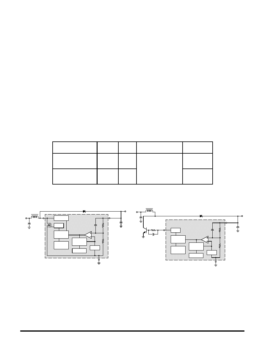
Motorola Master Selection Guide
Analog and Interface Integrated Circuits
4.2–6
Micropower Voltage Regulators for Portable Applications
(continued)
120 mA Micropower Voltage Regulator
MC78FC00H
TA = –30
°
to +80
°
C, Case 1213
The MC78FC00 series voltage regulators are specifically
designed for use as a power source for video instruments,
handheld communication equipment, and battery powered
equipment.
The MC78FC00 series voltage regulator ICs feature a high
accuracy output voltage and ultra–low quiescent current.
Each device contains a voltage reference unit, an error
amplifier, a driver transistor, and resistors for setting output
voltage, and a current limit circuit. These devices are avail-
able in SOT–89 surface mount packages, and allow
construction of an efficient, constant voltage power supply
circuit.
MC78FC00 Series Features:
•
Ultra–Low Quiescent Current of 1.1
µ
A Typical
•
Ultra–Low Dropout Voltage (100 mV at 10 mA)
•
Large Output Current (up to 120 mA)
•
Excellent Line Regulation (0.1%)
•
Wide Operating Voltage Range (2.0 V to 10 V)
•
High Accuracy Output Voltage (
±
2.5%)
•
Wide Output Voltage Range (2.0 V to 6.0 V)
•
Surface Mount Package (SOT–89)
ORDERING INFORMATION
Device
Output
Voltage
Operating
Temperature Range
Package
MC78FC30HT1
3.0
T
30
°
80
°
C
SOT 89
MC78FC33HT1
3.3
TA = –30
°
to +80
°
C
SOT–89
MC78FC40HT1
4.0
TA = –30
°
to +80
°
C
SOT–89
MC78FC50HT1
5.0
Other voltages from 2.0 to 6.0 V, in 0.1 V increments, are available upon
request. Consult factory for information.
2
Vin
1
Gnd
3
VO
Vref
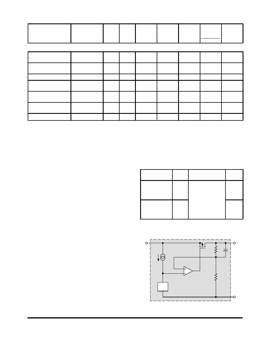
Micropower Voltage Regulator for External Power Transistor
MC78BC00N
TA = –30
°
to +80
°
C, Case 1212
The MC78BC00 voltage regulators are specifically
designed to be used with an external power transistor to
deliver high current with high voltage accuracy and low
quiescent current.
The MC78BC00 series are devices suitable for construct-
ing regulators with ultra–low dropout voltage and output cur-
rent in the range of several tens of mA to hundreds of mA.
These devices have a chip enable function, which minimizes
the standby mode current drain. Each of these devices con-
tains a voltage reference unit, an error amplifier, a driver tran-
sistor and feedback resistors. These devices are available in
the SOT–23, 5 pin surface mount packages.
These devices are ideally suited for battery powered
equipment, and power sources for hand–held audio instru-
ments, communication equipment and domestic appliances.
MC78BC00 Series Features:
•
Ultra–Low Supply Current (50
µ
A)
•
Standby Mode (0.2
µ
A)
•
Ultra–Low Dropout Voltage (0.1 V with External
Transistor and IO = 100 mA)
•
Excellent Line Regulation (Typically 0.1%/V)
•
High Accuracy Output Voltage (
±
2.5%)
ORDERING INFORMATION
Device
Output
Voltage
Operating
Temperature Range
Package
MC78BC30NTR
3.0
T
30
°
80
°
C
SOT 23
MC78BC33NTR
3.3
TA = –30
°
to +80
°
C
SOT–23
MC78BC40NTR
4.0
TA = –30
°
to +80
°
C
SOT–23
MC78BC50NTR
5.0
Other voltages from 2.0 to 6.0 V, in 0.1 V increments, are available upon
request. Consult factory for information.
2
Vin
1
Gnd
3
VO
4
Ext
5
CE
Vref
Motorola Master Selection Guide
Analog and Interface Integrated Circuits
4.2–7
Micropower Voltage Regulators for Portable Applications
(continued)
Low Noise 150 mA Low Drop Out (LDO) Linear Voltage Regulator
MC78PC00
TA = –40
°
to +85
°
C, Case 1212
The MC78PC00 are a series of CMOS linear voltage regu-
lators with high output voltage accuracy, low supply current,
low dropout voltage, and high Ripple Rejection. Each of
these voltage regulators consists of an internal voltage refer-
ence, an error amplifier, resistors, a current limiting circuit
and a chip enable circuit.
The dynamic Response to line and load is fast, which
makes these products ideally suited for use in hand–held
communication equipment.
The MC78PC00 series are housed in the SOT–23 5 lead
package, for maximum board space saving.
MC78PC00 Series Features:
•
Ultra–Low Supply Current: typical 35
m
A in ON mode with
no load
•
Standby Mode: typical 0.1
m
A
•
Low Dropout Voltage: typical 0.2 V @ IOUT = 100 mA
•
High Ripple Rejection: typical 70 dB @ f = 1 kHz
•
Low Temperature–Drift Coefficient of Output Voltage:
typical
±
100 ppm/
°
C
•
Excellent Line Regulation: typical 0.05%/V
•
High Accuracy Output Voltage:
±
2.0%
•
Fast Dynamic Response to Line and Load
•
Small Package: SOT–23 5 leads
•
Built–in Chip Enable circuit (CE input pin)
•
Similar Pinout to the LP2980/1/2 and MIC5205
ORDERING INFORMATION
Device
Operating
Temperature Range
Package
MC78PC28NTR
T
40
°
85
°
C
SOT 23
MC78PC30NTR
TA = –40
°
to +85
°
C
SOT–23
5 L
d
MC78PC33NTR
TA = –40
°
to +85
°
C
5 Leads
MC78PC50NTR
Other voltages are available. Consult your Motorola representative.
Block Diagram
1
VIN
5
VOUT
Vref
CE
3
2
GND
CURRENT LIMIT
MC78PCxx
Motorola Master Selection Guide
Analog and Interface Integrated Circuits
4.2–8
Micropower Voltage Regulators for Portable Applications
(continued)
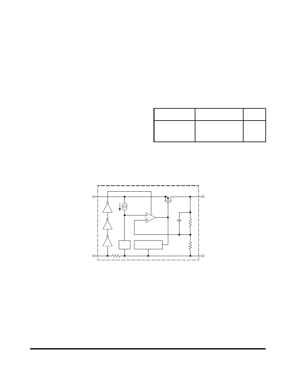
Micropower smallCAP
Voltage Regulators with On/Off Control
MC33264D, DM
TA = –40
°
to +85
°
C, Case 751, 846A
The MC33264 series are micropower low dropout voltage
regulators available in SO–8 and Micro–8 surface mount
packages and a wide range of output voltages. These de-
vices feature a very low quiescent current (100
µ
A in the ON
mode; 0.1
µ
A in the OFF mode), and are capable of supply-
ing output currents up to 100 mA. Internal current and ther-
mal limiting protection is provided. They require only a small
output capacitance for stability.
Additionally, the MC33264 has either active HIGH or ac-
tive LOW control (Pins 2 and 3) that allows a logic level signal
to turn–off or turn–on the regulator output.
Due to the low input–to–output voltage differential and
bias current specifications, these devices are ideally suited
for battery powered computer, consumer, and industrial
equipment where an extension of useful battery life is desir-
able.
MC33264 Features:
•
Low Quiescent Current (0.3
µ
A in OFF Mode; 95
µ
A in
ON Mode)
•
Low Input–to–Output Voltage Differential of 47 mV at
10 mA, and 131 mV at 50 mA
•
Multiple Output Voltages Available
•
Extremely Tight Line and Load Regulation
•
Stable with Output Capacitance of Only
0.22
µ
F for 4.0 V, 4.75 V and 5.0 V Output Voltages
0.33
µ
F for 2.8 V, 3.0 V, 3.3 V and 3.8 V Output Voltages
•
Internal Current and Thermal Limiting
•
Logic Level ON/OFF Control
•
Functionally Equivalent to TK115XXMC and LP2980
ORDERING INFORMATION
Device
Operating
Temperature Range
Package
MC33264D–2.8
T
40
°
85
°
C
SO 8
MC33264D–3.0
T
40
°
85
°
C
SO 8
MC33264D–3.3
T
40
°
85
°
C
SO 8
MC33264D–3.8
T
40
°
85
°
C
SO–8
MC33264D–4.0
T
40
°
85
°
C
MC33264D–4.75
T
40
°
85
°
C
MC33264D–5.0
TA = –40
°
to +85
°
C
MC33264DM–2.8
TA = –40
°
to +85
°
C
Mi
8
MC33264DM–3.0
Mi
8
MC33264DM–3.3
Mi
8
MC33264DM–3.8
Micro–8
MC33264DM–4.0
MC33264DM–4.75
MC33264DM–5.0
On/Off
Thermal and
Anti–Sat
Protection
1.23 V
Vref
VO
Base
Adj
Gnd
Vin
On/Off
1
2
3
8
7
6
5
MC33264
52.5 k
Rint

Motorola Master Selection Guide
Analog and Interface Integrated Circuits
4.2–9
Special Regulators
Voltage Regulator/Supervisory
Table 4. Voltage Regulator/Supervisory
D
i
Vout
(V)
IO
(mA)
Vin
(V)
Regline
Regload
TA
Suffix/
Device
Min
Max
(mA)
Max
Min
Max
Regline
(mV) Max
Regload
(mV) Max
TA
(
°
C)
Suffix/
Package
MC33128*
2.9
3.1
35
3.2
7.0
n/a
30
–30 to +60
D/751B
2.9
3.1
60
40
2.9
3.1
20
25
–2.65
–2.35
1.0
20
MC34160
4.75
5.25
100
7.0
40
40
50
0 to +70
P/648C,
DW/751G
MC33160
–40 to +85
DW/751G
MC33267
4.9
5.2
500
6.0
26
50
50
–40 to +105
T/314D,
TH, TV
MC33169*
4.7
6.4
–
2.7
9.5
–
–
–40 to +85
DTB/948G
6.4
7.0
–2.35
–2.65
*
These ICs are intended for powering cellular phone GaAs power amplifiers and can be used for other portable applications as well.

Motorola Master Selection Guide
Analog and Interface Integrated Circuits
4.2–10
Voltage Regulator/Supervisory
(continued)
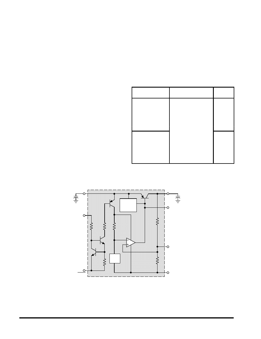
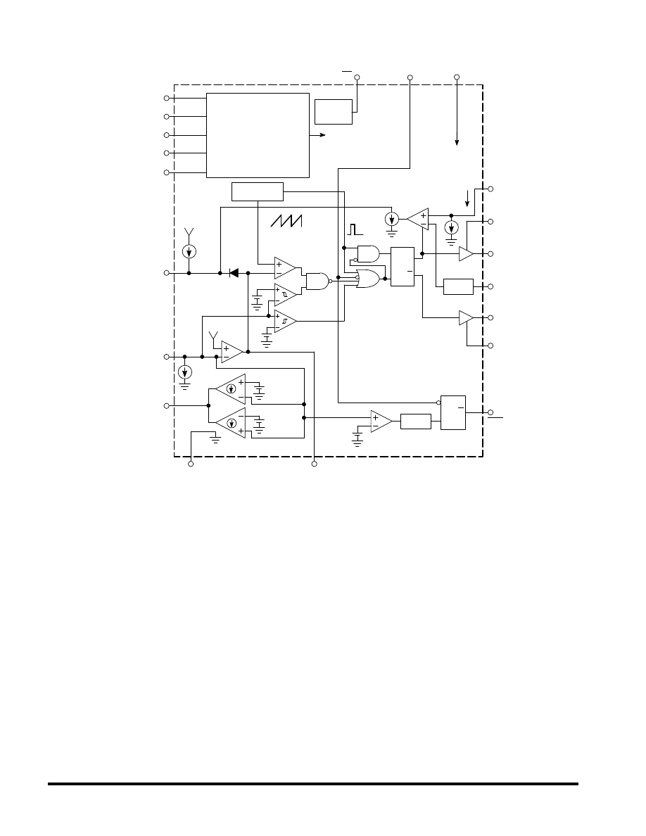
Microprocessor Voltage Regulator and Supervisory Circuit
MC34160P, DW
TA = 0
°
to +70
°
C, Case 648C, 751G
MC33160P, DW
TA = –40
°
to +85
°
C, Case 648C, 751G
The MC34160 series is a voltage
regulator and supervisory circuit contain-
ing many of the necessary monitoring
functions required in microprocessor
based systems. It is specifically designed
for appliance and industrial applications
offering the designer a cost effective
solution with minimal external components.
These integrated circuits feature a 5.0 V,
100 mA regulator with short circuit current
limiting, pinned out 2.6 V bandgap
reference, low voltage reset comparator,
power warning comparator with program-
mable hysteresis, and an uncommitted
comparator ideally suited for microproces-
sor line synchronization.
Additional features include a chip disable
input for low standby current, and internal
thermal shutdown for over temperature
protection.
These devices are contained in a 16 pin
dual–in–line heat tab plastic package for
improved thermal conduction.
Low Dropout Regulator
MC33267T, TV
TJ = –40
°
to +105
°
C, Case 314D, 314B
The MC33267 is a positive fixed 5.0 V
regulator that is specifically designed to
maintain proper voltage regulation with an
extremely low input–to–output voltage
differential. This device is capable of
supplying output currents in excess of 500
mA and contains internal current limiting and
thermal shutdown protection. Also featured
is an on–chip power–up reset circuit that is
ideally suited for use in microprocessor
based systems. Whenever the regulator
output voltage is below nominal, the reset
output is held low. A programmable time
delay is initiated after the regulator has
reached its nominal level and upon timeout,
the reset output is released.
Due to the low dropout voltage
specifications, the MC33267 is ideally
suited for use in battery powered industrial
and consumer equipment where an
extension of useful battery life is desirable.
This device is contained in an economical
five lead TO–220 type package.
VCC
Chip
Disable
Power
Sense
Hysteresis
Adjust
Noninverting
Input
Inverting
Input
14
15
9
10
2
1
Regulator
Output
Reset
Power
Warning
Reference
Output
Comparator
Output
Gnd
4, 5,12, 13
2.6 V
Reference
0.01R
0.913R
R
IH
IH “On”/“Off”
6
8
16
7
11
Thermal
Shutdown
Input
Output
1
5
Reference
1.25 V
Thermal
Over
Current
Detector
Ground
3
1.25 V
Delay
R
0.03
R
3.01
R
20
µ
A
3.8 V
Reset
200
Reset
2
Delay
4
+
+
Motorola Master Selection Guide
Analog and Interface Integrated Circuits
4.2–11
Voltage Regulator/Supervisory
(continued)
Very Low Dropout Regulator
L4949N, D
TJ = –40
°
to +125
°
C, Case 626, 751
The L4949 is a monolithic integrated
5.0 V voltage regulator with a very low
dropout and additional functions such as
power–on reset and input voltage sense.
It is designed for supplying the
micro–computer controlled systems
especially in automotive applications.
•
Operating DC Supply Voltage Range
5.0 V to 28 V
•
Transient Supply Voltage Up to 40 V
•
Extremely Low Quiescent Current in
Standby Mode
•
High Precision Standby Output Voltage
5.0 V
±
1%
•
Output Current Capability Up to
100 mA
•
Very Low Dropout Voltage Less Than
0.4 V
•
Reset Circuit Sensing The Output
Voltage
•
Programmable Reset Pulse Delay With
External Capacitor
•
Voltage Sense Comparator
•
Thermal Shutdown and Short Circuit
Protections
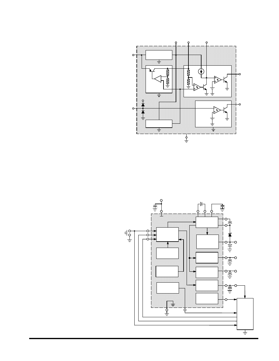
Power Management Controller
MC33128D
TA = –30
°
to +60
°
C, Case 751B
The MC33128 is a power management
controller specifically designed for use in
battery powered cellular telephone and
pager applications. This device contains all
of the active functions required to interface
the user to the system electronics via a
microprocessor. This integrated circuit
consists of a low dropout voltage regulator
with power–up reset for MPU power, two
low dropout voltage regulators for
independant powering of analog and digital
circuitry, and a negative charge pump
voltage regulator for full depletion of gallium
arsenide MESFETs.
Also included are protective system
shutdown features consisting of a battery
latch that is activated upon battery
insertion, low battery voltage shutdown,
and a thermal over temperature detector.
This device is available in a 16–pin narrow
body surface mount plastic package.
“On”/“Off”
Toggle
VCC
VBB CPC
VBB Output
Control
Logic
Low Battery
Shutdown
Thermal
Protection
Reference
Charge
Pump
Negative
Standby
Regulator
Standby
Regulator 1
Standby
Regulator 2
MPU
Regulator
MPU Power
Up Reset
Reference Output
Gnd
6
12
10
11
16
3
2
4
8
7
5
15
1
14
VDD
VSS
R
I
O
O
I
Output 4
CPC
Output 4
–2.5 V/1.0 mA
Output 1
3.0 V/30 mA
Output 2
3.0 V/60 mA
Output 3
3.0 V/20 mA
MPU
+
13
9
Regulator
1.23 Vref
2.0 V
2.0
µ
A
Reset
1.23 V
Sense
Gnd
Sense
Output
(So)
Reset
Sense
Input
(Si)
Supply
Voltage (VCC)
VZ
Output
Voltage (Vout)
CT
3
8
4
6
7
5
2
1
Vs
+
–
+
–
Preregulator
6.0 V

Motorola Master Selection Guide
Analog and Interface Integrated Circuits
4.2–12
GaAs Power Amplifier Support IC
MC33169DTB
TA = –40
°
to +85
°
C, Case 948G
The MC33169 is a support IC for GaAs
Power Amplifier Enhanced FETs used in
hand portable telephones such as GSM,
PCN and DECT. This device provides
negative voltages for full depletion of
Enhanced MESFETs as well as a priority
management system of drain switching,
ensuring that the negative voltage is always
present before turning “on” the Power
Amplifier. Additional features include an
idle mode input and a direct drive of the
N–Channel drain switch transistor.
This product is available in two versions,
– 2.5 and – 4.0 V. The – 4.0 V version is
intended for supplying RF modules for
GSM and DCS1800 applications, whereas
the – 2.5 V version is dedicated for DECT
and PHS systems.
•
Negative Regulated Output for Full
Depletion of GaAs MESFETs
•
Drain Switch Priority Management
Circuit
•
CMOS Compatible Inputs
•
Idle Mode Input (Standby Mode) for
Very Low Current Consumption
•
Output Signal Directly Drives
N–Channel FET
•
Low Startup and Operating Current
VBB Double
C3
VCC
+
–
C1
–
+
C2
VBB
Triple
C4
+
–
Tx Power
Control
Input
Idle
Mode Input
Gnd
Cp
+
–
VO
Output
(– 2.5 V or – 4.0 V)
Ci
Rf
Cf
+
–
+
RF
In
RF
Out
+
VBattery
(2.7 to 7.0 V)
Gate Drive Output
Sense Input
VBB
Generator
(Voltage Tripler)
Priority
Management
Negative
Generator
Charge
Pump
Power Amplifier
Sense
MC33169
MMSF4N01HD
2
1
14
8
10
4
5
7
6
13
9
3
11
+
12

Motorola Master Selection Guide
Analog and Interface Integrated Circuits
4.2–13
SCSI Regulator
Table 5. SCSI Regulator
D
i
Vout
(V)
Isink
Vin
(V)
Regline
Regload
TJ
Suffix/
Device
Min
Max
Isink
(mA)
Min
Max
Regline
(%)
Regload
(%)
TJ
(
°
C)
Suffix/
Package
MC34268
2.81
2.89
800
3.9
20
0.3
0.5
150
D/751, DT
SCSI–2 Active Terminator Regulator
MC34268D, DT
TJ = 0
°
to +125
°
C, Case 751, 369A
The MC34268 is a medium current, low dropout positive
voltage regulator specifically designed for use in SCSI–2
active termination circuits. This device offers the circuit
designer an economical solution for precision voltage
regulation, while keeping power losses to a minimum. The
regulator consists of a 1.0 V dropout composite PNP/NPN
pass transistor, current limiting, and thermal limiting. These
devices are packaged in the 8–pin SOP–8 and 3–pin DPAK
surface mount power packages.
Applications include active SCSI–2 terminators and post
regulation of switching power supplies.
•
2.85 V Output Voltage for SCSI–2 Active Termination
•
1.0 V Dropout
•
Output Current in Excess of 800 mA
•
Thermal Protection
•
Short Circuit Protection
•
Output Trimmed to 1.4% Tolerance
•
No Minimum Load Required
•
Space Saving DPAK and SOP–8 Surface Mount Power
Packages
Input
Thermal
Limiting
Control
Circuit
Current
Limit
Output
Ground
Motorola Master Selection Guide
Analog and Interface Integrated Circuits
4.2–14
Switching Regulator Control Circuits
These devices contain the primary building blocks which
are required to implement a variety of switching power
supplies. The product offerings fall into three major categories
consisting of single–ended and double–ended controllers,
plus single–ended ICs with on–chip power switch transistors.
These circuits operate in voltage, current or resonant modes
and are designed to drive many of the standard switching
topologies. The single–ended configurations include buck,
boost, flyback and forward converters. The double–ended
devices control push–pull, half bridge and full bridge
configurations.
Table 6. Single–Ended Controllers
These single–ended voltage and current mode controllers are designed for use in buck, boost, flyback, and forward
converters. They are cost effective in applications that range from 0.1 to 200 W power output.
IO
Minimum
Operating
Voltage
O
i
R f
Maximum
Useful
Oscillator
D
i
T
S ffi /
IO
(mA)
Max
Voltage
Range
(V)
Operating
Mode
Reference
(V)
Oscillator
Frequency
(kHz)
Device
TA
(
°
C)
Suffix/
Package
500
(U
i
d
7.0 to 40
Voltage
5.0
±
1.5%
200
MC34060A
0 to +70
D/751A
(Uncommitted
Drive Output)
P/646
Drive Output)
MC33060A
–40 to +85
D/751A
P/646
1000
(T t
P l MOSFET
4.2 to 12
Current
1.25
±
2.0%
300
MC34129
0 to +70
D/751A
(Totem Pole MOSFET
Drive Output)
P/646
Drive Output)
MC33129
–40 to +85
D/751A
P/646
11.5 to 30
5.0
±
2.0%
500
UC3842A
0 to +70
D/751A
N/626
11 to 30
5.0
±
1.0%
UC2842A
–25 to +85
D/751A
N/626
8.2 to 30
5.0
±
2.0%
UC3843A
0 to +70
D/751A
N/626
5.0
±
1.0%
UC2843A
–25 to +85
D/751A
N/626
11.5 to 30
5.0
±
2.0%
500
(50% D
UC3844
0 to +70
D/751A
(50% Duty
Cycle Limit)
N/626
11 to 30
5.0
±
1.0%
Cycle Limit)
UC2844
–25 to +85
D/751A
N/626
8.2 to 30
5.0
±
2.0%
UC3845
0 to +70
D/751A
N/626
5.0
±
1.0%
UC2845
–25 to +85
D/751A
N/626
11.5 to 30
5.0
±
2.0%
500
(Improved
UC3842B
0 to +70
D/751A
(Improved
Oscillator
D1/751
Oscillator
Specifications
with
N/626
with
Frequency
UC3842BV
–40 to +105
D/751A
Frequency
Guaranteed
at 250 kHz)
D1/751
at 250 kHz)
N/626

Motorola Master Selection Guide
Analog and Interface Integrated Circuits
4.2–15
Table 6. Single–Ended Controllers (continued)
These single–ended voltage and current mode controllers are designed for use in buck, boost, flyback, and forward
converters. They are cost effective in applications that range from 0.1 to 200 W power output.
IO
(mA)
Max
Suffix/
Package
TA
(
°
C)
Device
Maximum
Useful
Oscillator
Frequency
(kHz)
Reference
(V)
Operating
Mode
Minimum
Operating
Voltage
Range
(V)
IO
(mA)
Max
Suffix/
Package
TA
(
°
C)
Device
Maximum
Useful
Oscillator
Frequency
(kHz)
Reference
(V)
Operating
Mode
Minimum
Operating
Voltage
Range
(V)
1000
(T t
P l MOSFET
11 to 30
Current
5.0
±
1.0%
500
(I
d
UC2842B
–25 to +85
D/751A
(Totem Pole MOSFET
Drive Output)
(Improved
Oscillator
D1/751
Drive Output)
Oscillator
Specifications
N/626
8.2 to 30
5.0
±
2.0%
Specifications
with
F
UC3843B
0 to +70
D/751A
Frequency
Guaranteed
D1/751
Guaranteed
at 250 kHz)
N/626
at 250 kHz)
UC3843BV
–40 to +105
D/751A
D1/751
N/626
5.0
±
1.0%
UC2843B
–25 to +85
D/751A
D1/751
N/626
11.5 to 30
5.0
±
2.0%
500
(50% D
UC3844B
0 to +70
D/751A
(50% Duty
Cycle Limit)
D1/751
Cycle Limit)
N/626
UC3844BV
–40 to +105
D/751A
D1/751
N/626
11 to 30
5.0
±
1.0%
UC2844B
–25 to +85
D/751A
D1/751
N/626
8.2 to 30
5.0
±
2.0%
UC3845B
0 to +70
D/751A
D1/751
N/626
UC3845BV
–40 to +105
D/751A
D1/751
N/626
5.0
±
1.0%
UC2845B
–25 to +85
D/751A
D1/751
N/626
1000 Source
1500 Sink
(Split Totem Pole
Bipolar Drive Output)
11 to 18
5.0
±
6.0%
MC44602
P2/648C
2000
(T
P l MOSFET
9.2 to 30
Current
5.1
±
1.0%
1000
MC34023
0 to +70
DW/751G
(Totem Pole MOSFET
Drive Output)
or
Voltage
FN/775
Drive Output)
Voltage
P/648
MC33023
–40 to +105
DW/751G
FN/775
P/648
Motorola Master Selection Guide
Analog and Interface Integrated Circuits
4.2–16
Table 7. Single–Ended Controllers with On–Chip Power Switch
These monolithic power switching regulators contain all the active functions required to implement standard dc–to–dc
These monolithic power switching regulators contain all the active functions required to implement standard dc–to–dc
converter configurations with a minimum number of external components.
IO
Minimum
Operating
Voltage
O
i
R f
Maximum
Useful
Oscillator
D
i
T
S ffi /
IO
(mA)
Max
Voltage
Range
(V)
Operating
Mode
Reference
(V)
Oscillator
Frequency
(kHz)
Device
TA
(
°
C)
Suffix/
Package
1500
(U
itt d
2.5 to 40
Voltage
1.25
±
5.2%(1)
100
µ
A78S40
0 to +70
PC/648
(Uncommitted
Power Switch)
–40 to +85
PV/648
Power Switch)
1.25
±
2.0%
MC34063A
0 to +70
D/751
P1/626
MC33063A
–40 to +85
D/751
P1/626
–40 to +125
D/751
3400
(Uncommitted
2.5 to 40
Voltage
1.25
±
2.0%
and
100
MC34163
0 to +70
P/648C,
DW/751G
(Uncommitted
Power Switch)
and
5.05
±
3.0%
MC33163
–40 to +85
DW/751G
3400(2)
(Dedicated Emitter
7.5 to 40
5.05
±
2.0%
72
±
12%
Internally
MC34166
0 to +70
D2T/936A,
TH, TV,
(Dedicated Emitter
Power Switch)
Internally
Fixed
MC33166
–40 to +85
TH, TV,
T/314D
5500(3)
(Dedicated Emitter
MC34167
0 to +70
(Dedicated Emitter
Power Switch)
MC33167
–40 to +85
(1) Tolerance applies over the specified operating temperature range.
(2) Guaranteed minimum, typically 4300 mA.
(3) Guaranteed minimum, typically 6500 mA.
Table 8. Easy Switcher
Single–Ended Controllers with On–Chip Power Switch
The Easy Switcher
series is ideally suited for easy, convenient design of a step–down switching regulator (buck converter),
with a minimum number of external components.
IO
Minimum
Operating
Voltage
O
i
Oscillator
Output
D
i
T
S ffi /
IO
(mA)
Max
Voltage
Range
(V)
Operating
Mode
Oscillator
Frequency
(kHz)
Output
Voltage
(V)
Device
TJ
(
°
C)
Suffix/
Package
500
4.75 to 40
Voltage
52 Fixed
3.3
LM2574N–3.3
–40 to +125
N/626
500
4.75 to 40
8.0 to 40
Voltage
52 Fixed
Internal
3.3
5.0
LM2574N 3.3
LM2574N–5
40 to +125
N/626
15 to 40
18 t 40
12
15
LM2574N–12
LM2574N 15
18 to 40
8 0 to 40
15
1 23 to 37
LM2574N–15
LM2574N ADJ
8.0 to 40
1.23 to 37
LM2574N–ADJ
1000
4.75 to 40
Voltage
52 Fixed
3.3
LM2575T–3.3
–40 to +125
T/314D
1000
4.75 to 40
8.0 to 40
Voltage
52 Fixed
Internal
3.3
5.0
LM2575T 3.3
LM2575T–5
40 to +125
T/314D
15 to 40
18 t 40
12
15
LM2575T–12
LM2575T 15
18 to 40
8 0 to 40
15
1 23 to 37
LM2575T–15
LM2575T ADJ
8.0 to 40
1.23 to 37
LM2575T–ADJ
4.75 to 40
3.3
LM2575TV–3.3
TV/314B
4.75 to 40
8.0 to 40
3.3
5.0
LM2575TV 3.3
LM2575TV–5
TV/314B
15 to 40
18 t 40
12
15
LM2575TV–12
LM2575TV 15
18 to 40
8 0 to 40
15
1 23 to 37
LM2575TV–15
LM2575TV ADJ
8.0 to 40
1.23 to 37
LM2575TV–ADJ
4.75 to 40
3.3
LM2575D2T–3.3
D2T/936A
4.75 to 40
8.0 to 40
3.3
5.0
LM2575D2T 3.3
LM2575D2T–5
D2T/936A
15 to 40
18 t 40
12
15
LM2575D2T–12
LM2575D2T 15
18 to 40
8 0 to 40
15
1 23 to 37
LM2575D2T–15
LM2575D2T ADJ
8.0 to 40
1.23 to 37
LM2575D2T–ADJ

Motorola Master Selection Guide
Analog and Interface Integrated Circuits
4.2–17
Table 8. Easy Switcher
Single–Ended Controllers with On–Chip Power Switch (continued)
The Easy Switcher
series is ideally suited for easy, convenient design of a step–down switching regulator (buck converter),
with a minimum number of external components.
IO
(mA)
Max
Suffix/
Package
TJ
(
°
C)
Device
Output
Voltage
(V)
Oscillator
Frequency
(kHz)
Operating
Mode
Minimum
Operating
Voltage
Range
(V)
IO
(mA)
Max
Suffix/
Package
TJ
(
°
C)
Device
Output
Voltage
(V)
Oscillator
Frequency
(kHz)
Operating
Mode
Minimum
Operating
Voltage
Range
(V)
3000
4.75 to 40
Voltage
52 Fixed
3.3
LM2576T–3.3
–40 to +125
T/314D
3000
4.75 to 40
8.0 to 40
Voltage
52 Fixed
Internal
3.3
5.0
LM2576T 3.3
LM2576T–5
40 to +125
T/314D
15 to 40
18 t 40
12
15
LM2576T–12
LM2576T 15
18 to 40
8 0 to 40
15
1 23 to 37
LM2576T–15
LM2576T ADJ
8.0 to 40
1.23 to 37
LM2576T–ADJ
4.75 to 40
3.3
LM2576TV–3.3
TV/314B
4.75 to 40
8.0 to 40
3.3
5.0
LM2576TV 3.3
LM2576TV–5
TV/314B
15 to 40
18 t 40
12
15
LM2576TV–12
LM2576TV 15
18 to 40
8 0 to 40
15
1 23 to 37
LM2576TV–15
LM2576TV ADJ
8.0 to 40
1.23 to 37
LM2576TV–ADJ
4.75 to 40
3.3
LM2576D2T–3.3
D2T/936A
4.75 to 40
8.0 to 40
3.3
5.0
LM2576D2T 3.3
LM2576D2T–5
D2T/936A
15 to 40
18 t 40
12
15
LM2576D2T–12
LM2576D2T 15
18 to 40
8 0 to 40
15
1 23 to 37
LM2576D2T–15
LM2576D2T ADJ
8.0 to 40
1.23 to 37
LM2576D2T–ADJ
Table 9. Very High Voltage Single–Ended Controller with On–Chip Power Switch
This monolithic high voltage switching regulator is specifically designed to operate from a rectified ac line voltage source.
g
g
g
g
p
y
g
p
g
Included are an on–chip high voltage power switch, active off–line startup circuitry and a full featured PWM controller with fault
protection.
Power Switch
Maximum Rating
Startup
O
i
Feedback
Maximum
Useful
Oscillator
D
i
T
S ffi /
VDS (V)
IDS (mA)
Startup
Input Max
(V)
Operating
Mode
Feedback
Threshold
(V)
Oscillator
Frequency
(kHz)
Device
TJ
(
°
C)
Suffix/
Package
500
2000
250
Voltage
2.6
±
3.1%
1000
MC33362
–25 to +125
DW/751N,
P/648E
700
1000
450
MC33363
P/648E
700
1000
450
MC33363A
Table 10. Double–Ended Controllers
These double–ended voltage, current and resonant mode controllers are designed for use in push–pull, half–bridge, and
full–bridge converters. They are cost effective in applications that range from 100 to 2000 watts power output.
IO
Minimum
Operating
Voltage
O
i
R f
Maximum
Useful
Oscillator
D
i
T
S ffi /
IO
(mA)
Max
Voltage
Range
(V)
Operating
Mode
Reference
(V)
Oscillator
Frequency
(kHz)
Device
TA
(
°
C)
Suffix/
Package
500
(U
itt d
7.0 to 40
Voltage
5.0
±
5.0%(1)
200
TL494
0 to +70
CN/648
(Uncommitted
Drive Outputs)
–25 to +85
IN/648
Drive Outputs)
5.0
±
1.5%
300
TL594
0 to +70
CN/648
–25 to +85
IN/648
±
500
(Totem Pole MOSFET
Drive Outputs)
8.0 to 40
5.1
±
2.0%
400
SG3525A
0 to +70
N/648
±
200
(Totem Pole MOSFET
Drive Outputs)
5.0
±
2.0%
SG3526
0 to +125(2)
N/707

Motorola Master Selection Guide
Analog and Interface Integrated Circuits
4.2–18
Table 10. Double–Ended Controllers (continued)
These double–ended voltage, current and resonant mode controllers are designed for use in push–pull, half–bridge, and
full–bridge converters. They are cost effective in applications that range from 100 to 2000 watts power output.
IO
(mA)
Max
Suffix/
Package
TA
(
°
C)
Device
Maximum
Useful
Oscillator
Frequency
(kHz)
Reference
(V)
Operating
Mode
Minimum
Operating
Voltage
Range
(V)
IO
(mA)
Max
Suffix/
Package
TA
(
°
C)
Device
Maximum
Useful
Oscillator
Frequency
(kHz)
Reference
(V)
Operating
Mode
Minimum
Operating
Voltage
Range
(V)
±
1500
(T t
P l MOSFET
9.6 to 20
Resonant
(Z
5.1
±
2.0%
1000
MC34066
0 to +70
DW/751G
(Totem Pole MOSFET
Drive Outputs)
(Zero
Current)
P/648
Drive Outputs)
Current)
MC33066
–40 to +85
DW/751G
P/648
Resonant
(Z
2000
MC34067
0 to +70
DW/751G
(Zero
Voltage)
P/648
Voltage)
MC33067
–40 to +85
DW/751G
P/648
2000
(T t
P l MOSFET
9.2 to 30
Current
5.1
±
1.0%
1000
MC34025
0 to +70
DW/751G
(Totem Pole MOSFET
Drive Outputs)
or
Voltage
FN/775
Drive Outputs)
Voltage
P/648
MC33025
–40 to +105
DW/751G
FN/775
P/648
(1) Tolerance applies over the specified operating temperature range.
(2) Junction Temperature Range.

Motorola Master Selection Guide
Analog and Interface Integrated Circuits
4.2–19
Switching Regulator Control Circuits
(continued)
CMOS Micropower DC–to–DC Converters
Variable Frequency Micropower DC–to–DC Converter
MC33463H
TA = –30
°
to +80
°
C, Case 1213
The MC33463 series are micropower step–up switching
voltage regulators, specifically designed for handheld and
laptop applications, to provide regulated output voltages
using a minimum of external parts. A wide choice of output
voltages are available. These devices feature a very low
quiescent bias current of 4.0
µ
A typical.
The MC33463H–XXKT1 series features a highly accurate
voltage reference, an oscillator, a variable frequency modula-
tion (VFM) controller, a driver transistor (Lx), a comparator
and feedback resistive divider.
T h e M C 3 3 4 6 3 H – X X LT 1 i s i d e n t i c a l t o t h e
MC33463H–XXKT1, except that a drive pin (EXT) for an
external transistor is provided.
Due to the low bias current specifications, these devices
are ideally suited for battery powered computer, consumer,
and industrial equipment where an extension of useful bat-
tery life is desirable.
MC33463 Series Features:
•
Low Quiescent Bias Current of 4.0
µ
A
•
High Output Voltage Accuracy of
±
2.5%
•
Low Startup Voltage of 0.9 V at 1.0 mA
•
Wide Output Voltage Range of 2.5 V to 7.5 V Available
•
High Efficiency of 80% Typical
•
Surface Mount Package
ORDERING INFORMATION
Device
Output
Voltage
Type
Operating
Temperature Range
Package
(Tape/Reel)
MC33463H–30KT1
3.0
Int.
S it h
T
30
°
80
°
C
SOT–89
(T
)
MC33463H–33KT1
3.3
Switch
T
30
°
80
°
C
(Tape)
MC33463H–50KT1
5.0
TA = –30
°
to +80
°
C
MC33463H–30LT1
3.0
Ext.
S it h
TA = –30
°
to +80
°
C
SOT–89
(T
)
MC33463H–33LT1
3.3
Switch
D i
(Tape)
MC33463H–50LT1
5.0
Drive
Other voltages from 2.5 V to 7.5 V, in 0.1 V increments are available. Consult factory for information.
MC33463H–XXKT1
MC33463H–XXLT1
XX Denotes Output Voltage
Lx
D
Vin
VLx Limitier
3
Vref
Gnd
VFM
Controller
100 kHz
Oscillator
2
Output
VO
CO
Drive
VFM
Controller
100 kHz
Oscillator
Vref
D
Vin
Output
VO
CO
Gnd
1
3
EXT
L
Q
Rb
Cb
1
2
Drive
L
Cin
Cin
Motorola Master Selection Guide
Analog and Interface Integrated Circuits
4.2–20
CMOS Micropower DC–to–DC Converters
(continued)
Fixed Frequency PWM Micropower DC–to–DC Converter
MC33466H
TA = –30
°
to +80
°
C, Case 1213
The MC33466 series are micropower switching voltage
regulators, specifically designed for handheld and laptop
applications, to provide regulated output voltages using a
minimum of external parts. A wide choice of output voltages
are available. These devices feature a very low quiescent
bias current of 15
µ
A typical.
The MC33466H–XXJT1 series features a highly accurate
voltage reference, an oscillator, a pulse width modulation
(PWM) controller, a driver transistor (Lx), an error amplifier
and feedback resistive divider.
T h e M C 3 3 4 6 6 H – X X LT 1 i s i d e n t i c a l t o t h e
MC33466H–XXJT1, except that a drive pin (EXT) for an
external transistor is provided.
Due to the low bias current specifications, these devices
are ideally suited for battery powered computer, consumer,
and industrial equipment where an extension of useful bat-
tery life is desirable.
MC33466 Series Features:
•
Low Quiescent Bias Current of 15
µ
A
•
High Output Voltage Accuracy of
±
2.5%
•
Low Startup Voltage of 0.9 V at 1.0 mA
•
Soft–Start = 500
µ
s
•
Surface Mount Package
ORDERING INFORMATION
Device
Output
Voltage
Type
Operating
Temperature Range
Package
(Tape/Reel)
MC33466H–30JT1
3.0
Int.
S it h
T
30
°
80
°
C
SOT–89
(T
)
MC33466H–33JT1
3.3
Switch
T
30
°
80
°
C
(Tape)
MC33466H–50JT1
5.0
TA = –30
°
to +80
°
C
MC33466H–30LT1
3.0
Ext.
S it h
TA = –30
°
to +80
°
C
SOT–89
(T
)
MC33466H–33LT1
3.3
Switch
D i
(Tape)
MC33466H–50LT1
5.0
Drive
Other voltages from 2.5 V to 7.5 V, in 0.1 V increments are available. Consult factory for information.
Gnd
Drive
PWM
Controller
50 kHz
Oscillator
Vref
1
2
VO
MC33466H–XXJT1
MC33466H–XXLT1
Phase
Comp
Soft–Start
Output
(Voltage
Feedback)
3
EXT
Gnd
Drive
PWM
Controller
50 kHz
Oscillator
Vref
1
2
VO
Phase
Comp
Soft–Start
Output
(Voltage
Feedback)
3
VLx Limiter
Lx
Vin
Vin
XX Denotes Output Voltage
CO
CO
D
D
L
L
Rb
Cb
Q
Cin
Cin

Motorola Master Selection Guide
Analog and Interface Integrated Circuits
4.2–21
Switching Regulator Control Circuits
(continued)
Synchronous Rectification DC/DC Converter
Programmable Integrated Controller
MC33470
TA = 0
°
to +75
°
C, Case 751D
The MC33470 is a digitally programmable switching volt-
age regulator, specifically designed for Microprocessor sup-
ply, Voltage Regulator Module and general purpose applica-
tions, to provide a high power regulated output voltage using
a minimum of external parts. A 5–bit digital–to–analog con-
verter defines the dc output voltage.
This product has three additional features. The first is a
pair of high speed comparators which monitor the output volt-
age and expedite the circuit response to load current
changes. The second feature is a soft start circuit which esta-
blishes a controlled response when input power is applied
and when recovering from external circuit fault conditions.
The third feature is two output drivers which provide synchro-
nous rectification for optimum efficiency.
This product is ideally suited for computer, consumer, and
industrial equipment where accuracy, efficiency and optimum
regulation performance is desirable.
MC33470 Features:
•
5–Bit Digital–to–Analog Converter Allows Digital Control
of Output Voltage
•
High Speed Response to Transient Load Conditions
•
Output Enable Pin Provides On/Off Control
•
Programmable Soft Start Control
•
High Current Output Drives for Synchronous Rectification
•
Internally Trimmed Reference with Low Temperature
Coefficient
•
Programmable Overcurrent Protection
•
Overvoltage Fault Indication
•
Functionally Similar to the LTC1553
ORDERING INFORMATION
Device
Operating
Temperature Range
Package
MC33470DW
TA = 0
°
to +75
°
C
SO–20L
Motorola Master Selection Guide
Analog and Interface Integrated Circuits
4.2–22
Oscillator
PWM
Comparator
OTA Error Amp
VCC
Sense
Compensation
PGnd
G1
G2
Ifb
Over Current
Detect
Outen
Power
Good
VID0
VID1
VID2
VID3
Vref
VCC
Voltage
Identification
Code
Input
Digitally Programmed
Reference
VCC
Vref
R
S
Q
PWM
Latch
+
0.96 Vref
1.04 Vref
5
VID4
18
17
16
15
14
4
10
9
14
3
1
8
20
2
19
0.93 Vref
1.04 Vref
13
AGnd
6
SS
800
µ
Over
Temp
11
Imax
7
10
µ
A
2.5 V
1.5 V
En
90
µ
A
190
µ
A
S
R
Q
Delay
Fault
1.14 Vref
20
µ
A
OT
Q
+
+
+
Delay
Simplified Block Diagram
PV
CC

Motorola Master Selection Guide
Analog and Interface Integrated Circuits
4.2–23
Switching Regulator Control Circuits
(continued)
Easy Switcher
Single–Ended Controllers with On–Chip Power Switch
Step–Down Voltage Regulators
LM2574N–XX
TJ = –40
°
to +125
°
C, Case 626
The LM2574 series of regulators are monolithic integrated
circuits ideally suited for easy and convenient design of a
step–down switching regulator (buck converter). All circuits
of this series are capable of driving a 0.5 A load with excellent
line and load regulation. These devices are available in fixed
output voltages of 3.3 V, 5.0 V, 12 V, 15 V, and an adjustable
output version.
These regulators were designed to minimize the number
of external components to simplify the power supply design.
Standard series of inductors optimized for use with the
LM2574 are offered by several different inductor manufactur-
ers.
Since the LM2574 converter is a switch–mode power sup-
ply, its efficiency is significantly higher in comparison with
popular three–terminal linear regulators, especially with high-
er input voltages. In most cases, the power dissipated by the
LM2574 regulator is so low, that the copper traces on the
printed circuit board are normally the only heatsink needed
and no additional heatsinking is required.
The LM2574 features include a guaranteed
±
4% tolerance
on output voltage within specified input voltages and output
load conditions, and
±
10% on the oscillator frequency (
±
2%
over 0
°
C to +125
°
C). External shutdown is included, featur-
ing 60
µ
A (typical) standby current. The output switch in-
cludes cycle–by–cycle current limiting, as well as thermal
shutdown for full protection under fault conditions.
Features
•
3.3 V, 5.0 V, 12 V, 15 V, and Adjustable Output Versions
•
Adjustable Version Output Voltage Range, 1.23 to 37 V
±
4% max over Line and Load Conditions
•
Guaranteed 0.5 A Output Current
•
Wide Input Voltage Range: 4.75 to 40 V
•
Requires Only 4 External Components
•
52 kHz Fixed Frequency Internal Oscillator
•
TTL Shutdown Capability, Low Power Standby Mode
•
High Efficiency
•
Uses Readily Available Standard Inductors
•
Thermal Shutdown and Current Limit Protection
Applications
•
Simple and High–Efficiency Step–Down (Buck)
Regulators
•
Efficient Pre–Regulator for Linear Regulators
•
On–Card Switching Regulators
•
Positive to Negative Converters (Buck–Boost)
•
Negative Step–Up Converters
•
Power Supply for Battery Chargers
XX = Voltage Option, i.e., 3.3, 5, 12, 15 V; and ADJ for
Adjustable Output
Representative Block Diagram and Typical Application
Unregulated
DC Input
+Vin
5
Cout
Feedback
1
Cin
L1
D1
R2
R1
1.0 k
Output
7
Pwr Gnd
4
ON/OFF
3
Reset
Latch
Thermal
Shutdown
52 kHz
Oscillator
1.235 V
Band–Gap
Reference
Freq
Shift
18 kHz
Comparator
Fixed Gain
Error Amplifier
Current
Limit
Driver
1.0 Amp
Switch
ON/OFF
3.1 V Internal
Regulator
Vout
Load
Output
Voltage Versions
3.3 V
5.0 V
12 V
15 V
R2
(
Ω
)
1.7 k
3.1 k
8.84 k
11.3 k
For adjustable version
R1 = open, R2 = 0
Ω
Sig Gnd
2

Motorola Master Selection Guide
Analog and Interface Integrated Circuits
4.2–24
Step–Down Voltage Regulators
(continued)
LM2575T–XX, TV, D2T, LM2576T–XX, TV, D2T
TJ = –40
°
to +125
°
C, Case 314D, 314B, 936A
The LM2575/6 series of regulators are monolithic inte-
grated circuits ideally suited for easy and convenient design
of a step–down switching regulator (buck converter). All cir-
cuits of this series are capable of driving a 1.0 A (LM2575) or
3.0 A (LM2576) load with excellent line and load regulation.
These devices are available in fixed output voltages of 3.3 V,
5.0 V, 12 V, 15 V, and an adjustable output version.
These regulators were designed to minimize the number
of external components to simplify the power supply design.
Standard series of inductors optimised for use with the
LM2575/6 are offered by several different inductor manufac-
turers.
Since the LM2575/6 converter is a switch–mode power
supply, its efficiency is significantly higher in comparison with
popular three–terminal linear regulators, especially with high-
er input voltages. In many cases, the power dissipated by the
LM2575/6 regulator is so low, that no heatsink is required or
its size could be reduced dramatically.
The LM2575/6 features include a guaranteed
±
4% toler-
ance on output voltage within specified input voltages and
output load conditions, and
±
10% on the oscillator frequency
(
±
2% over 0
°
C to 125
°
C). External shutdown is included, fea-
turing 80
µ
A typical standby current. The output switch in-
cludes cycle–by–cycle current limiting, as well as thermal
shutdown for full protection under fault conditions.
Features
•
3.3 V, 5.0 V, 12 V, 15 V, and Adjustable Output Versions
•
Adjustable Version Output Voltage Range of 1.23 V to
37 V
±
4% Maximum Over Line and Load Conditions
•
Guaranteed 1.0 A (LM2575) 3.0 A (LM2576)
Output Current
•
Wide Input Voltage Range: 4.75 V to 40 V
•
Requires Only 4 External Components
•
52 kHz Fixed Frequency Internal Oscillator
•
TTL Shutdown Capability, Low Power Standby Mode
•
High Efficiency
•
Uses Readily Available Standard Inductors
•
Thermal Shutdown and Current Limit Protection
Applications
•
Simple and High–Efficiency Step–Down (Buck)
Regulators
•
Efficient Pre–Regulator for Linear Regulators
•
On–Card Switching Regulators
•
Positive to Negative Converters (Buck–Boost)
•
Negative Step–Up Converters
•
Power Supply for Battery Chargers
XX = Voltage Option, i.e., 3.3, 5, 12, 15 V; and ADJ for
Adjustable Output
Representative Block Diagram and Typical Application
Unregulated
DC Input
+Vin
1
Cout
Feedback
4
Cin
L1
D1
R2
R1
1.0 k
Output
2
Gnd
3
ON/OFF
5
Reset
Latch
Thermal
Shutdown
52 kHz
Oscillator
1.235 V
Band–Gap
Reference
Freq
Shift
18 kHz
Comparator
Fixed Gain
Error Amplifier
Current
Limit
Driver
1.0 Amp
Switch
ON/OFF
3.1 V Internal
Regulator
Regulated
Output
Vout
Load
Output
Voltage Versions
3.3 V
5.0 V
12 V
15 V
R2
(
Ω
)
1.7 k
3.1 k
8.84 k
11.3 k
For adjustable version
R1 = open, R2 = 0
Ω
This device contains 162 active transistors.

Motorola Master Selection Guide
Analog and Interface Integrated Circuits
4.2–25
Switching Regulator Control Circuits
(continued)
Single–Ended GreenLine
Controllers
Enhanced Mixed Frequency Mode GreenLine
PWM Controller:
Fixed Frequency, Variable Frequency, Standby Mode
MC44603AP, DW
TA = –25
°
to +85
°
C, Case 648, 751G
The MC44603A is an enhanced high performance control-
ler that is specifically designed for off–line and dc–to–dc con-
verter applications. This device has the unique ability of auto-
matically changing operating modes if the converter output is
overloaded, unloaded, or shorted, offering the designer addi-
tional protection for increased system reliability. The
MC44603A has several distinguishing features when
compared to conventional SMPS controllers. These features
consist of a foldback facility for overload protection, a
standby mode when the converter output is slightly loaded, a
demagnetization detection for reduced switching stresses on
transistor and diodes, and a high current totem pole output
ideally suited for driving a power MOSFET. It can also be
used for driving a bipolar transistor in low power converters
(< 150 W). It is optimized to operate in discontinuous mode
but can also operate in continuous mode. Its advanced
design allows use in current mode or voltage mode control
applications.
Current or Voltage Mode Controller
•
Operation up to 250 kHz Output Switching Frequency
•
Inherent Feed Forward Compensation
•
Latching PWM for Cycle–by–Cycle Current Limiting
•
Oscillator with Precise Frequency Control
High Flexibility
•
Externally Programmable Reference Current
•
Secondary or Primary Sensing
•
Synchronization Facility
•
High Current Totem Pole Output
•
Undervoltage Lockout with Hysteresis
Safety/Protection Features
•
Overvoltage Protection Against Open Current and Open
Voltage Loop
•
Protection Against Short Circuit on Oscillator Pin
•
Fully Programmable Foldback
•
Soft–Start Feature
•
Accurate Maximum Duty Cycle Setting
•
Demagnetization (Zero Current Detection) Protection
•
Internally Trimmed Reference
•
Enhanced Output Drive
GreenLine Controller: Low Power Consumption in
Standby Mode
•
Low Startup and Operating Current
•
Fully Programmable Standby Mode
•
Controlled Frequency Reduction in Standby Mode
•
Low dV/dT for Low EMI Radiations
High Safety Standby Ladder Mode GreenLine
PWM Controller
MC44604P
TA = –25
°
to +85
°
C, Case 648
The MC44604 is an enhanced high performance controller
that is specifically designed for off–line and dc–to–dc con-
verter applications.
The MC44604 is a modification of the MC44603. The
MC44604 offers enhanced safety and reliable power man-
agement in its protection features (foldback, overvoltage
detection, soft–start, accurate demagnetization detection).
Its high current totem pole output is also ideally suited for
driving a power MOSFET but can also be used for driving a
bipolar transistor in low power converters (< 150 W).
In addition, the MC44604 offers a new efficient way to
reduce the standby operating power by means of a patented
standby ladder mode operation of the converter significantly
reducing the converter consumption in standby mode.
Current or Voltage Mode Controller
•
Operation Up to 250 kHz Output Switching Frequency
•
Inherent Feed Forward Compensation
•
Latching PWM for Cycle–by–Cycle Current Limiting
•
Oscillator with Precise Frequency Control
High Flexibility
•
Externally Programmable Reference Current
•
Secondary or Primary Sensing
•
High Current Totem Pole Output
•
Undervoltage Lockout with Hysteresis
Safety/Protection Features
•
Overvoltage Protection Facility Against Open Loop
•
Protection Against Short Circuit on Oscillator Pin
•
Fully Programmable Foldback
•
Soft–Start Feature
•
Accurate Maximum Duty Cycle Setting
•
Demagnetization (Zero Current Detection) Protection
•
Internally Trimmed Reference
GreenLine
Controller:
•
Low Startup and Operating Current
•
Patented Standby Ladder Mode for Low Standby Losses
•
Low dV/dT for Low EMI

Motorola Master Selection Guide
Analog and Interface Integrated Circuits
4.2–26
Single–Ended GreenLine
Controllers
(continued)
High Safety Latched Mode GreenLine
PWM Controller
for (Multi)Synchronized Applications
MC44605P
TA = –25
°
to +85
°
C, Case 648
The MC44605 is a high performance current mode con-
troller that is specifically designed for off–line converters. The
MC44605 has several distinguishing features that make it
particularly suitable for multisynchronized monitor applica-
tions.
The MC44605 synchronization arrangement enables
operation from 16 kHz up to 130 kHz. This product was
optimized to operate with universal ac mains voltage from
80 V to 280 V, and its high current totem pole output makes
it ideally suited for driving a power MOSFET.
The MC44605 protections provide well controlled, safe
power management. Safety enhancements detect four differ-
ent fault conditions and provide protection through a disab-
ling latch.
Current or Voltage Mode Controller
•
Current Mode Operation Up to 250 kHz Output Switching
Frequency
•
Inherent Feed Forward Compensation
•
Latching PWM for Cycle–by–Cycle Current Limiting
•
Oscillator with Precise Frequency Control
•
Externally Programmable Reference Current
•
Secondary or Primary Sensing (Availability of Error
Amplifier Output)
•
Synchronization Facility
•
High Current Totem Pole Output
•
Undervoltage Lockout with Hysteresis
•
Low Output dV/dT for Low EMI
•
Low Startup and Operating Current
Safety/Protection Features
•
Soft–Start Feature
•
Demagnetization (Zero Current Detection) Protection
•
Overvoltage Protection Facility Against Open Loop
•
EHT Overvoltage Protection (E.H.T.OVP): Protection
Against Excessive Amplitude Synchronization Pulses
•
Winding Short Circuit Detection (W.S.C.D.)
•
Limitation of the Maximum Input Power (M.P.L.):
Calculation of Input Power for Overload Protection
•
Over Heating Detection (O.H.D.): to Prevent the Power
Switch from Excessive Heating
Latched Disabling Mode
•
When one of the following faults is detected: EHT
overvoltage, Winding Short Circuit (WSCD), excessive
input power (M.P.L.), power switch over heating (O.H.D.),
a counter is activated
•
If the counter is activated for a time that is long enough,
the circuit gets definitively disabled. The latch can only be
reset by removing and then re–applying power
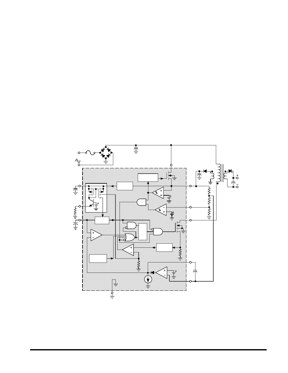
Motorola Master Selection Guide
Analog and Interface Integrated Circuits
4.2–27
Switching Regulator Control Circuits
(continued)
Very High Voltage Switching Regulator
MC33362DW, P
TJ = –25
°
to +125
°
C, Case 751N, 658E
The MC33362 is a monolithic high voltage switching
regulator that is specifically designed to operate from a
rectified 120 VAC line source. This integrated circuit features
an on–chip 500 V/2.0 A SenseFET power switch, 250 V active
off–line startup FET, duty cycle controlled oscillator, current
limiting comparator with a programmable threshold and
leading edge blanking, latching pulse width modulator for
double pulse suppression, high gain error amplifier, and a
trimmed internal bandgap reference. Protective features
include cycle–by–cycle current limiting, input undervoltage
lockout with hysteresis, output overvoltage protection, and
thermal shutdown. This device is available in a 16–lead
dual–in–line and wide body surface mount packages.
•
On–Chip 500 V, 2.0 A SenseFET Power Switch
•
Rectified 120 VAC Line Source Operation
•
On–Chip 250 V Active Off–Line Startup FET
•
Latching PWM for Double Pulse Suppression
•
Cycle–By–Cycle Current Limiting
•
Input Undervoltage Lockout with Hysteresis
•
Output Overvoltage Protection Comparator
•
Trimmed Internal Bandgap Reference
•
Internal Thermal Shutdown
20 W Off–Line Converter
Startup
Reg
Osc
Thermal
LEB
PWM
DC Output
Startup Input
Gnd
4, 5, 12, 13
Mirror
7
AC Input
Regulator
Output
6
8
CT
RT
PWM Latch
EA
Ipk
VCC
3
11
16
9
10
1
Compensation
Voltage Feedback
Input
Power Switch
Drain
Overvoltage
Protection Input
Driver
OVP
UVLO
S
R
Q
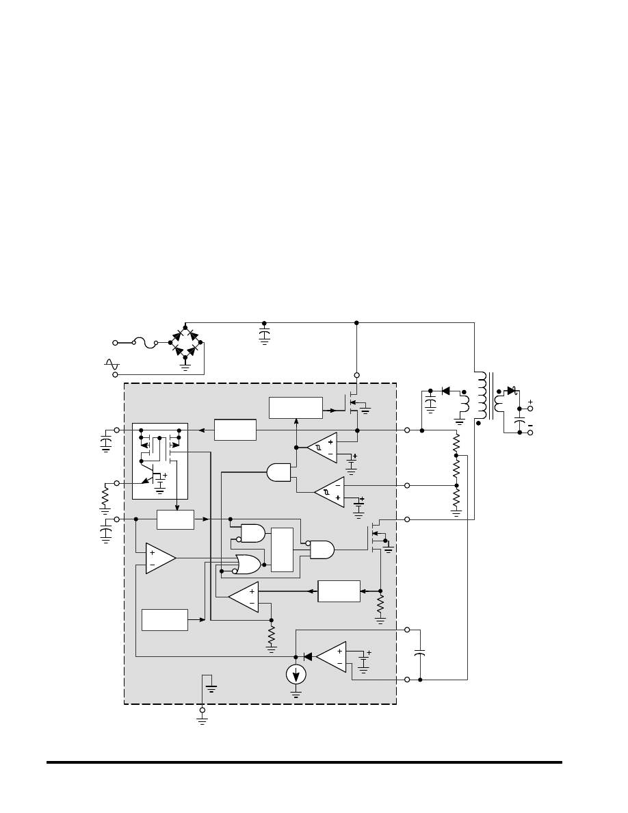
Motorola Master Selection Guide
Analog and Interface Integrated Circuits
4.2–28
Switching Regulator Control Circuits
(continued)
Very High Voltage Switching Regulator
MC33363DW, P, MC33363ADW, AP
TJ = –25
°
to +125
°
C, Case 751N, 648E
The MC33363 is a monolithic high voltage switching regu-
lator that is specifically designed to operate from a rectified
240 Vac line source. This integrated circuit features an on–
chip 700 V/1.0 A (1.5 A in MC33363A) SenseFET power
switch, 450 V (500 V in MC33363A) active off–line startup
FET, duty cycle controlled oscillator, current limiting
comparator with a programmable threshold and leading edge
blanking, latching pulse width modulator for double pulse
suppression, high gain error amplifier, and a trimmed internal
bandgap reference. Protective features include cycle–by–
cycle current limiting, input undervoltage lockout with hyster-
esis, output overvoltage protection, and thermal shutdown.
This device is available in a 16–lead dual–in–line and wide
body surface mount packages.
•
On–Chip 700 V, 1.0 A SenseFET Power Switch
•
On–Chip 700 V, 1.5 A SenseFET Power Switch
in MC33363A
•
Rectified 240 Vac Line Source Operation
•
On–Chip 450 V Active Off–Line Startup FET
•
On–Chip 500 V Active Off–Line Startup FET
in MC33363A
•
Latching PWM for Double Pulse Suppression
•
Cycle–By–Cycle Current Limiting
•
Input Undervoltage Lockout with Hysteresis
•
Output Overvoltage Protection Comparator
•
Trimmed Internal Bandgap Reference
•
Internal Thermal Shutdown
Startup
Reg
Osc
Thermal
LEB
PWM
DC Output
Startup Input
Gnd
4, 5, 12, 13
Mirror
7
AC Input
Regulator
Output
6
8
CT
RT
PWM Latch
EA
Ipk
VCC
3
11
16
9
10
1
Compensation
Voltage
Feedback
Input
Power Switch
Drain
Overvoltage
Protection Input
Driver
OVP
UVLO
S
R
Q

Motorola Master Selection Guide
Analog and Interface Integrated Circuits
4.2–29
Switching Regulator Control Circuits
(continued)
High Voltage Switching Regulator
MC33363B
TJ = –25
°
to +125
°
C, Case 751G, 648E
The MC33363B is a monolithic high voltage switching reg-
ulator that is specifically designed to operate from a rectified
240 Vac line source. This integrated circuit features an
on–chip 700 V/1.0 A SenseFET power switch, 450 V active
off–line startup FET, duty cycle controlled oscillator, current
limiting comparator with a programmable threshold and lead-
ing edge blanking, latching pulse width modulator for double
pulse suppression, high gain error amplifier, and a trimmed
internal bandgap reference. Protective features include
cycle–by–cycle current limiting, input undervoltage lockout
with hysteresis, overvoltage protection, and thermal shut-
down. This device is available in a 16–lead dual–in–line and
wide body surface mount packages.
•
On–Chip 700 V, 1.0 A SenseFET Power Switch
•
Rectified 240 Vac Line Source Operation
•
On–Chip 450 V Active Off–Line Startup FET
•
Latching PWM for Double Pulse Suppression
•
Cycle–By–Cycle Current Limiting
•
Input Undervoltage Lockout with Hysteresis
•
Output Overvoltage Protection
•
Trimmed Internal Bandgap Reference
•
Internal Thermal Shutdown
ORDERING INFORMATION
Device
Operating
Temperature Range
Package
MC33363BDW
TJ = –25
°
to +125
°
C
SOP–16L
MC33363BP
TJ = –25
°
to +125
°
C
DIP–16
Simplified Application
Startup
Reg
Osc
Thermal
LEB
PWM
DC Output
Startup Input
Gnd
4, 5, 12, 13
Mirror
7
AC Input
Regulator
Output
6
8
CT
RT
PWM Latch
EA
Ipk
VCC
3
11
16
9
10
1
Compensation
Voltage
Feedback
Input
Power Switch
Drain
Overvoltage
Protection
Input
Driver
OVP
UVLO
S
R
Q

Motorola Master Selection Guide
Analog and Interface Integrated Circuits
4.2–30
Switching Regulator Control Circuits
(continued)
Critical Conduction SMPS Controller
MC33364D, D1, D2
TJ = –25
°
to +125
°
C, Case 751, 751B
The MC33364 series are variable frequency SMPS control-
lers that operate in the critical conduction mode. They are opti-
mized for low power, high density power supplies requiring
minimum board area, reduced component count, and low
power dissipation. Each narrow body SOIC package provides
a small footprint. Integration of the high voltage startup saves
approximately 0.7 W of power compared to resistor boot-
strapped circuits.
Each MC33364 features an on–board reference, UVLO
function, a watchdog timer to initiate output switching, a zero
current detector to ensure critical conduction operation, a
current sensing comparator, leading edge blanking, and a
CMOS driver. Protection features include the ability to shut
down switching, and cycle–by–cycle current limiting.
The MC33364D1 is available in a surface mount SO–8
package. It has an internal 126 kHz frequency clamp. For
loads which have a low power operating condition, the fre-
quency clamp limits the maximum operating frequency, pre-
venting excessive switching losses and EMI radiation.
The MC33364D2 is available in the SO–8 package without
an internal frequency clamp.
The MC33364D is available in the SO–16 package. It
has an internal 126 kHz frequency clamp which is pinned
out, so that the designer can adjust the clamp frequency
by connecting appropriate values of resistance and
capacitance.
•
Lossless Off–Line Startup
•
Leading Edge Blanking for Noise Immunity
•
Watchdog Timer to Initiate Switching
•
Minimum Number of Support Components
•
Shutdown Capability
•
Over Temperature Protection
•
Optional Frequency Clamp
Current
Sense
FB
ZC Det
VCC
Gate
PWM
Comparator
S
R
Q
Gnd
Line
Vref
Vref
UVLO
Restart
Delay
R
Leading
Edge
Blanking
Zero
Current
Detector
Watchdog
Timer
Thermal
Shutdown
Bandgap
Reference
VCC
UVLO
Frequency
Clamp
Optional
Frequency
Clamp
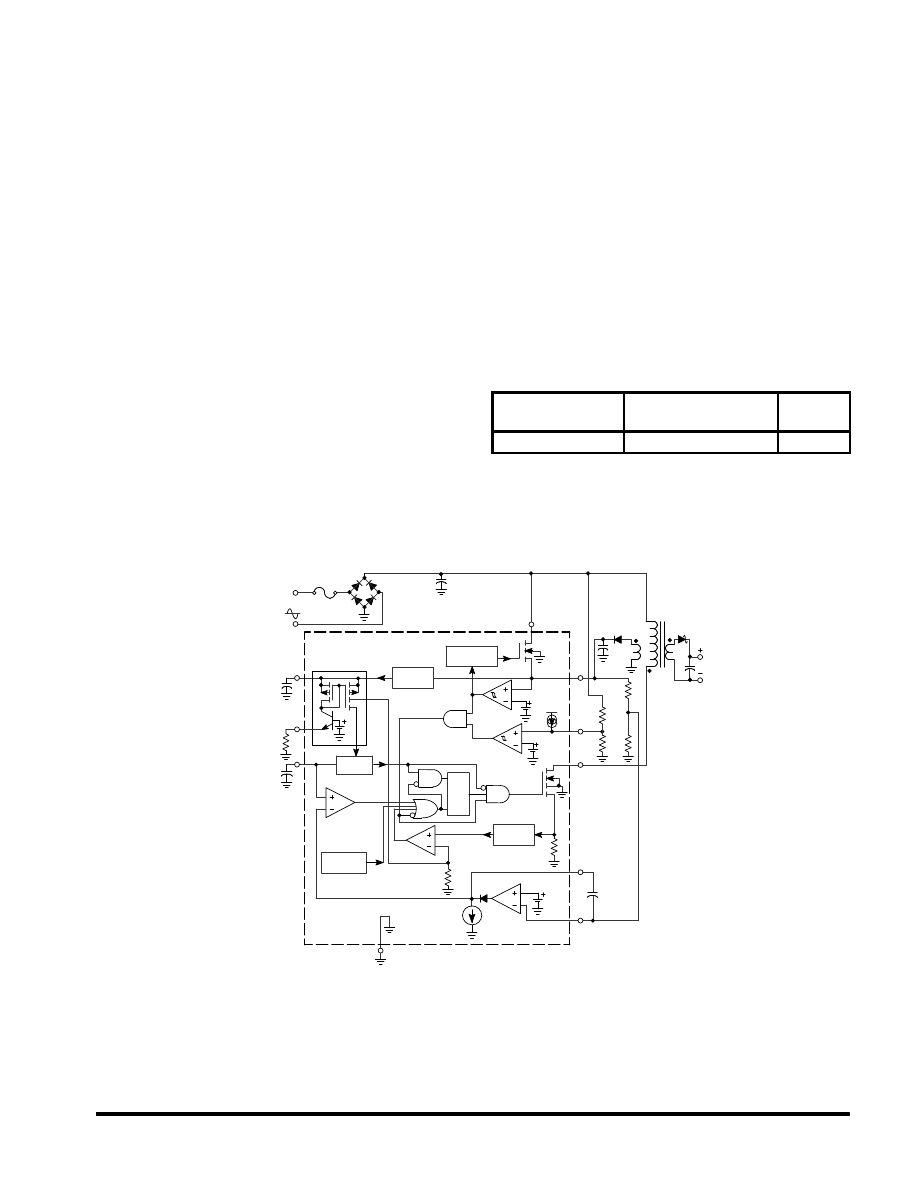
Motorola Master Selection Guide
Analog and Interface Integrated Circuits
4.2–31
Switching Regulator Control Circuits
(continued)
High Voltage Switching Regulator
MC33365
TJ = –25
°
to +125
°
C, Case 648E
The MC33365 is a monolithic high voltage switching regu-
lator that is specifically designed to operate from a rectified
240 Vac line source. This integrated circuit features an
on–chip 700 V/1.0 A SenseFET power switch, 450 V active
off–line startup FET, duty cycle controlled oscillator, current
limiting comparator with a programmable threshold and lead-
ing edge blanking, latching pulse width modulator for double
pulse suppression, high gain error amplifier, and a trimmed
internal bandgap reference. Protective features include
cycle–by–cycle current limiting, input undervoltage lockout
with hysteresis, bulk capacitor voltage sensing, and thermal
shutdown. This device is available in a 16–lead dual–in–line
package.
•
On–Chip 700 V, 1.0 A SenseFET Power Switch
•
Rectified 240 Vac Line Source Operation
•
On–Chip 450 V Active Off–Line Startup FET
•
Latching PWM for Double Pulse Suppression
•
Cycle–By–Cycle Current Limiting
•
Input Undervoltage Lockout with Hysteresis
•
Bulk Capacitor Voltage Comparator
•
Trimmed Internal Bandgap Reference
•
Internal Thermal Shutdown
ORDERING INFORMATION
Device
Operating
Temperature Range
Package
MC33365P
TJ = –25
°
to +125
°
C
DIP–16
Simplified Application
Startup
Reg
Osc
Thermal
LEB
PWM
DC Output
Startup Input
Gnd
4, 5, 12, 13
Mirror
7
AC Input
Regulator
Output
6
8
CT
RT
PWM Latch
EA
Ipk
VCC
3
11
16
9
10
1
Compensation
Voltage
Feedback
Input
Power Switch
Drain
BOK
Driver
BOK
UVLO
S
R
Q
Motorola Master Selection Guide
Analog and Interface Integrated Circuits
4.2–32
Special Switching Regulator Controllers
These high performance dual channel controllers are
optimized for off–line, ac–to–dc power supplies and dc–to–dc
converters in the flyback topology. They also have
undervoltage lockout voltages which are optimized for off–line
and lower voltage dc–to–dc converters, respectively.
Applications include desktop computers, peripherals,
televisions, games, and various consumer appliances.
Table 11. Dual Channel Controllers
IO
Minimum
Operating
Voltage
O
i
R f
Maximum
Useful
Oscillator
D
i
T
S ffi /
IO
(mA)
Max
Voltage
Range
(V)
Operating
Mode
Reference
(V)
Oscillator
Frequency
(kHz)
Device
TA
(
°
C)
Suffix/
Package
500
4.0
Voltage
1.25
±
2.0%
700
MC34270
0 to +70
FB/873A
MC34271
±
1000
(T t
P l MOSFET
11 to 15.5
Current
5.0
±
2.6%
500
MC34065
0 to +70
DW/751G
(Totem Pole MOSFET
Drive Outputs)
P/648
Drive Outputs)
MC33065
–40 to +85
DW/751G
P/648
11 to 20
MC34065
0 to +70
DW–H/751G
P–H/648
MC33065
–40 to +85
DW–H/751G
P–H/648
8.4 to 20
MC34065
0 to +70
DW–L/751G
P–L/648
MC33065
–40 to +85
DW–L/751G
P–L/648
Table 12. Universal Microprocessor Power Supply Controllers
A versatile power supply control circuit for microprocessor–based systems, this device is mainly intended for automotive
applications and battery powered instruments. The circuit provides a power–on reset delay and a Watchdog feature for orderly
microprocessor operation.
Regulated
Output
VCC
(V)
Reference
Key
Supervisory
D
i
TA
Regulated
Outputs
Output
Current (mA)
Min
Max
Reference
(V)
Supervisory
Features
Device
TA
(
°
C)
Package
E2PROM Programmable
Output:
24 V (Write Mode)
5.0 V (Read Mode)
150 peak
6.0
35
2.5
±
3.2%
MPU Reset and
Watchdog
Circuit
TCF5600
–40 to +85
707
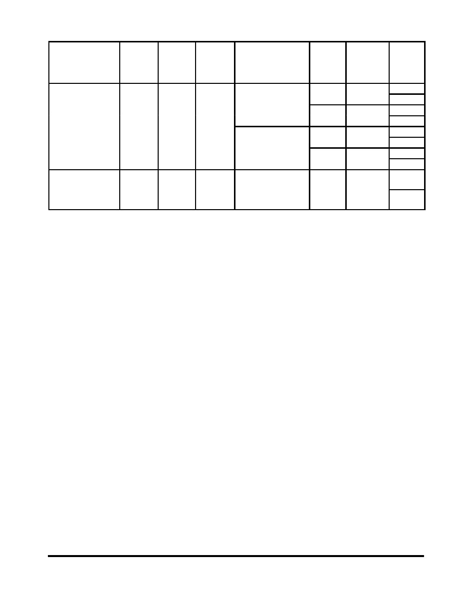
Motorola Master Selection Guide
Analog and Interface Integrated Circuits
4.2–33
Table 13. Power Factor Controllers
IO
Minimum
Operating
Voltage
Maximum
Startup
R f
F
D
i
T
S ffi /
IO
(mA)
Max
Voltage
Range
(V)
Startup
Voltage
(V)
Reference
(V)
Features
Device
TA
(
°
C)
Suffix/
Package
±
500
(T t
P l MOSFET
9.0 to 30
30
2.5
±
1.4%
Undervoltage Lockout,
I t
l St t
MC34261
0 to +70
D/751
(Totem Pole MOSFET
Drive Outputs)
Internal Startup
Timer
P/626
Drive Outputs)
Timer
MC33261
–40 to +85
D/751
P/626
Overvoltage
C
t
MC34262
0 to +85
D/751
Comparator,
Undervoltage Lockout,
P/626
Undervoltage Lockout,
Internal Startup
Ti
MC33262
–40 to +105
D/751
p
Timer
P/626
1500
(CMOS Totem Pole
MOSFET Drive
9.0 to 16
500
5.0
±
1.5%
Off–Line High Voltage
Startup Overvoltage
Comparator
MC33368
–25 to +125
D/751K
MOSFET Drive
Outputs)
Comparator,
Undervoltage Lockout,
Timer, Low Load Detect
P/648
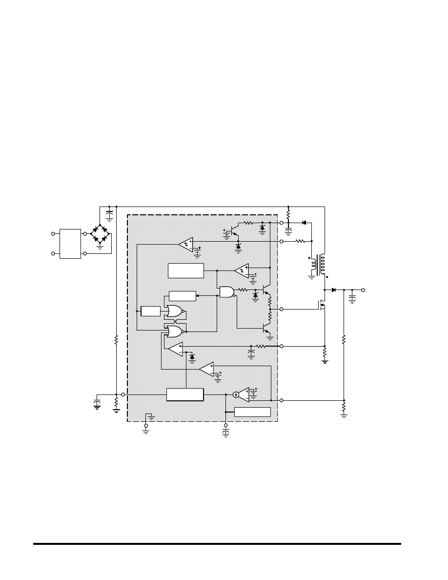
Motorola Master Selection Guide
Analog and Interface Integrated Circuits
4.2–34
Power Factor Controllers
MC34262D, P
TA = 0
°
to +85
°
C, Case 751, 626
MC33262D, P
TA = –40
°
to +105
°
C, Case 751, 626
The MC34262, MC33262 series are active power factor
controllers specifically designed for use as a preconverter in
electronic ballast and in off–line power converter applications.
These integrated circuits feature an internal startup timer for
stand alone applications, a one quadrant multiplier for near
unity power factor, zero current detector to ensure critical
conduction operation, transconductance error amplifier,
quickstart circuit for enhanced startup, trimmed internal
bandgap reference, current sensing comparator, and a totem
pole output ideally suited for driving a power MOSFET.
Also included are protective features consisting of an
overvoltage comparator to eliminate runaway output voltage
due to load removal, input undervoltage lockout with
hysteresis, cycle–by–cycle current limiting, multiplier output
clamp that limits maximum peak switch current, an RS latch
for single pulse metering, and a drive output high state clamp
for MOSFET gate protection. These devices are available in
dual–in–line and surface mount plastic packages.
14 V
0.68
1.5 V
Error Amp
Overvoltage
Comparator
1.08 Vref
Quickstart
10
µ
A
10 pF
20 k
1.6 V
Timer R
330
100
MTP
14N50E
1.3 M
RFI
Filter
0.01
MC34262
6.7 V
Zero Current
Detector
T
UVLO
Current Sense
Comparator
RS
Latch
1.2 V
36 V
2.5 V
Reference
16 V
10
Drive
Output
Multiplier
Delay
85 to 265
Vac
1
12 k
22 k
100 k
1N4934
10 k
1.6 M
0.1
MUR460
VO
400 V/0.44 A
Vref
10
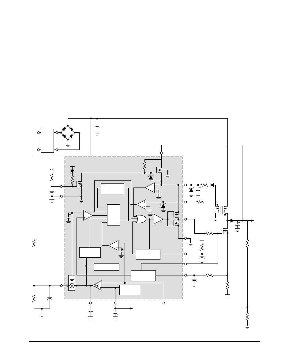
Motorola Master Selection Guide
Analog and Interface Integrated Circuits
4.2–35
Power Factor Controllers
(continued)
MC33368D, P
TJ = –25
°
to +125
°
C, Case 751K, 648
The MC33368 is an active power factor controller that
functions as a boost preconverter in off–line power supply
applications. MC33368 is optimized for low power, high
density power supplies requiring minimum board area,
reduced component count, and low power dissipation. The
narrow body SOIC package provides a small footprint.
Integration of the high voltage startup saves approximately
0.7 W of power compared to resistor bootstrapped circuits.
The MC33368 features a watchdog timer to initiate output
switching, a one quadrant multiplier to force the line current to
follow the instantaneous line voltage, a zero current detector
to ensure critical conduction operation, a transconductance
error amplifier, a current sensing comparator, a 5.0 V
reference, an undervoltage lockout (UVLO) circuit which
monitors the VCC supply voltage, and a CMOS driver for
driving MOSFETs. The MC33368 also includes a
programmable output switching frequency clamp. Protection
features include an output overvoltage comparator to
minimize overshoot, a restart delay timer, and cycle–by–
cycle current limiting.
•
Lossless Off–Line Startup
•
Output Overvoltage Comparator
•
Leading Edge Blanking (LEB) for Noise Immunity
•
Watchdog Timer to Initiate Switching
•
Restart Delay Timer
Multiplier
8
C1
1.0
Frequency
Clamp
R
S
Q
R
S
S
Timer
R
Vref
Leading Edge
Blanking
Low
Load Detect
Comp
FB
6
LEB
13
PGnd
Gate
ZCD
VCC
Line
RD
AGnd
MC33368
16
12
7
11
10
FC
9
3
1
4
Quickstart
Overvoltage
Comparator
Set Dominant
1.5 V
15 V
Q
5.0 V
Reference
400 V
MUR460
D5
C3
330
MTW20N50E
Q1
D6
C4
100
T
R4
22 k
EMI
Filter
92 to
270 Vac
R7
0.1
C5
1.0
R5
1.3 M
R3
10.5 k
C2
0.01
R1
10 k
R2
820 k
R8
1.0 M
C9
330
µ
F
D1
D3
D2
D4
R11
10
15 V
C6
0.1
13/8.0
UVLO
1.2/1.0
R13
51
D8
RS Latch
Vref
Vref
Vref
CS
2
5
Mult
1.5 V
Zero
Current
Detect
1.08 x Vref
1N5406
R10
10 k
C7
470 pF
Vref
C8
0.001
R9
10
1N4744
1N4934
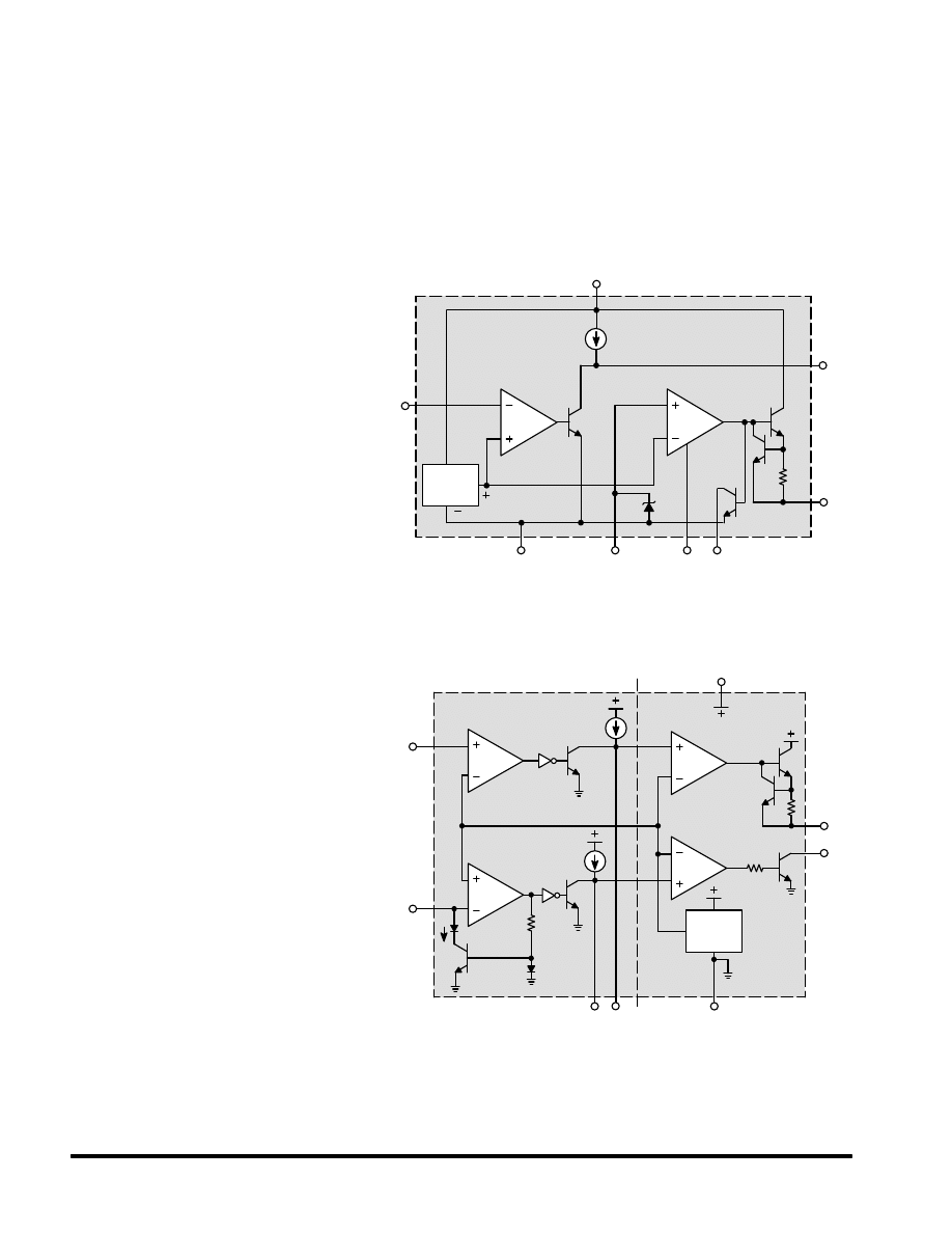
Motorola Master Selection Guide
Analog and Interface Integrated Circuits
4.2–36
Supervisory Circuits
A variety of Power Supervisory Circuits are offered.
Overvoltage sensing circuits which drive ‘‘Crowbar’’ SCRs
are provided in several configurations from a low cost
three–terminal version to 8–pin devices which provide
pin–programmable trip voltages or additional features, such
as an indicator output drive and remote activation capability.
An over/undervoltage protection circuit is also offered.
Overvoltage Crowbar Sensing Circuit
MC3423P1, D
TA = 0
°
to +70
°
C, Case 626, 751
This device can protect sensitive
circuitry from power supply transients or
regulator failure when used with an external
‘‘Crowbar’’ SCR. The device senses
voltage and compares it to an internal 2.6 V
reference. Overvoltage trip is adjustable by
means of an external resistive voltage
divider. A minimum duration before trip is
programmable with an external capacitor.
Other features include a 300 mA high
current output for driving the gate of a
‘‘Crowbar’’ SCR, an open–collector
indicator output and remote activation
capability.
Over/Undervoltage Protection Circuit
MC3425P1
TA = 0
°
to +70
°
C, Case 626
The MC3425 is a power supply
supervisory circuit containing all the
necessary functions required to monitor
over and undervoltage fault conditions.
This device features dedicated over and
undervoltage sensing channels with
independently programmable time delays.
The overvoltage channel has a high current
drive output for use in conjunction with an
external SCR ‘‘Crowbar’’ for shutdown. The
undervoltage channel input comparator
has hysteresis which is externally
programmable, and an open–collector
output for fault indication.
OV
Sense
UV
Sense
VCC
OV
Drive
UV
Indicator
Input Section
Output Section
UV
DLY
OV
DLY
Gnd
200
µ
A
200
µ
A
12.5
µ
A
IH
2.5 V
Vref
VCC
Sense 1
Current
Source
Output
VEE
Sense 2
Remote
Activation
Indicator
Output
Vref
2.6 V
200
µ
A
2
1
4
8
6
5
3
7
8
1
6
3
4
5
2
7
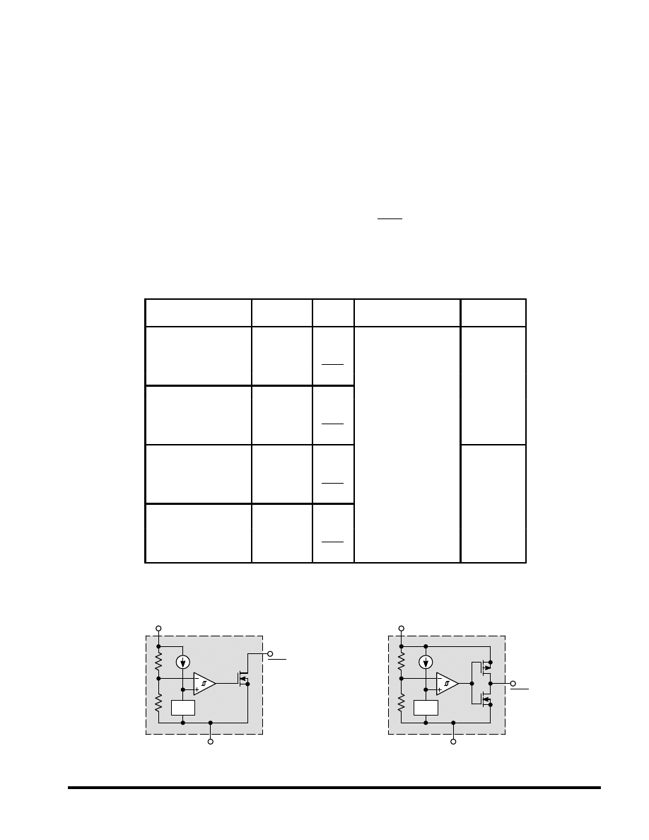
Motorola Master Selection Guide
Analog and Interface Integrated Circuits
4.2–37
Supervisory Circuits
(continued)
Micropower Undervoltage Sensing Circuits
MC33464H, N
TA = –30
°
to +80
°
C, Case 1213, 1212
The MC33464 series are micropower undervoltage sensing
circuits that are specifically designed for use with battery
powered microprocessor based systems, where extended
battery life is required. A choice of several threshold voltages
from 0.9 V to 4.5 V are available. These devices feature a very
low quiescent bias current of 0.8
µ
A typical.
The MC33464 series features a highly accurate voltage
reference, a comparator with precise thresholds and built–in
hysteresis to prevent erratic reset operation, a choice of out-
put configurations between open drain or complementary
MOS, and guaranteed operation below 1.0 V with extremely
low standby current. These devices are available in either
SOT–89 3–pin or SOT–23 5–pin surface mount packages.
Applications include direct monitoring of the MPU/logic
power supply used in portable, appliance, automotive and
industrial equipment.
MC33464 Features:
•
Extremely Low Standby Current of 0.8
µ
A at Vin = 1.5 V
•
Wide Input Voltage Range (0.7 V to 10 V)
•
Monitors Power Supply Voltages from 1.1 V to 5.0 V
•
High Accuracy Detector Threshold (
±
2.5%)
•
Two Reset Output Types (Open Drain or Complementary
Drive)
•
Two Surface Mount Packages (SOT–89 or SOT–23
5–Pin)
ORDERING INFORMATION
Device
Threshold
Voltage
Type
Operating
Temperature Range
Package
(Qty/Reel)
MC33464H–09AT1
0.9
O
T
30
°
80
°
C
SOT 89
MC33464H–20AT1
2.0
Open
T
30
°
80
°
C
SOT 89
MC33464H–27AT1
2.7
Drain
T
30
°
80
°
C
SOT 89
MC33464H–30AT1
3.0
Reset
T
30
°
80
°
C
SOT 89
MC33464H–45AT1
4.5
Reset
T
30
°
80
°
C
SOT–89
MC33464H–09CT1
0.9
C
l
T
30
°
80
°
C
SOT 89
(1000)
MC33464H–20CT1
2.0
Compl.
T
30
°
80
°
C
MC33464H–27CT1
2.7
MOS
T
30
°
80
°
C
MC33464H–30CT1
3.0
Reset
T
30
°
80
°
C
MC33464H–45CT1
4.5
Reset
TA = –30
°
to +80
°
C
MC33464N–09ATR
0.9
O
TA = –30
°
to +80
°
C
SOT 23
MC33464N–20ATR
2.0
Open
SOT 23
MC33464N–27ATR
2.7
Drain
SOT 23
MC33464N–30ATR
3.0
Reset
SOT 23
MC33464N–45ATR
4.5
Reset
SOT–23
MC33464N–09CTR
0.9
C
l
SOT 23
(3000)
MC33464N–20CTR
2.0
Compl.
MC33464N–27CTR
2.7
MOS
MC33464N–30CTR
3.0
Reset
MC33464N–45CTR
4.5
Reset
Other voltages from 0.9 to 6.0 V, in 0.1 V increments, are available. Consult factory for information.
MC33464X–YYATZ
Open Drain Configuration
MC33464X–YYCTZ
Complementary Drive Configuration
X Denotes Package Type
YY Denotes Threshold Voltage
TZ Denotes Taping Type
Vref
2
Input
1
Reset
3
Gnd
Vref
2
Input
1
Reset
3
Gnd
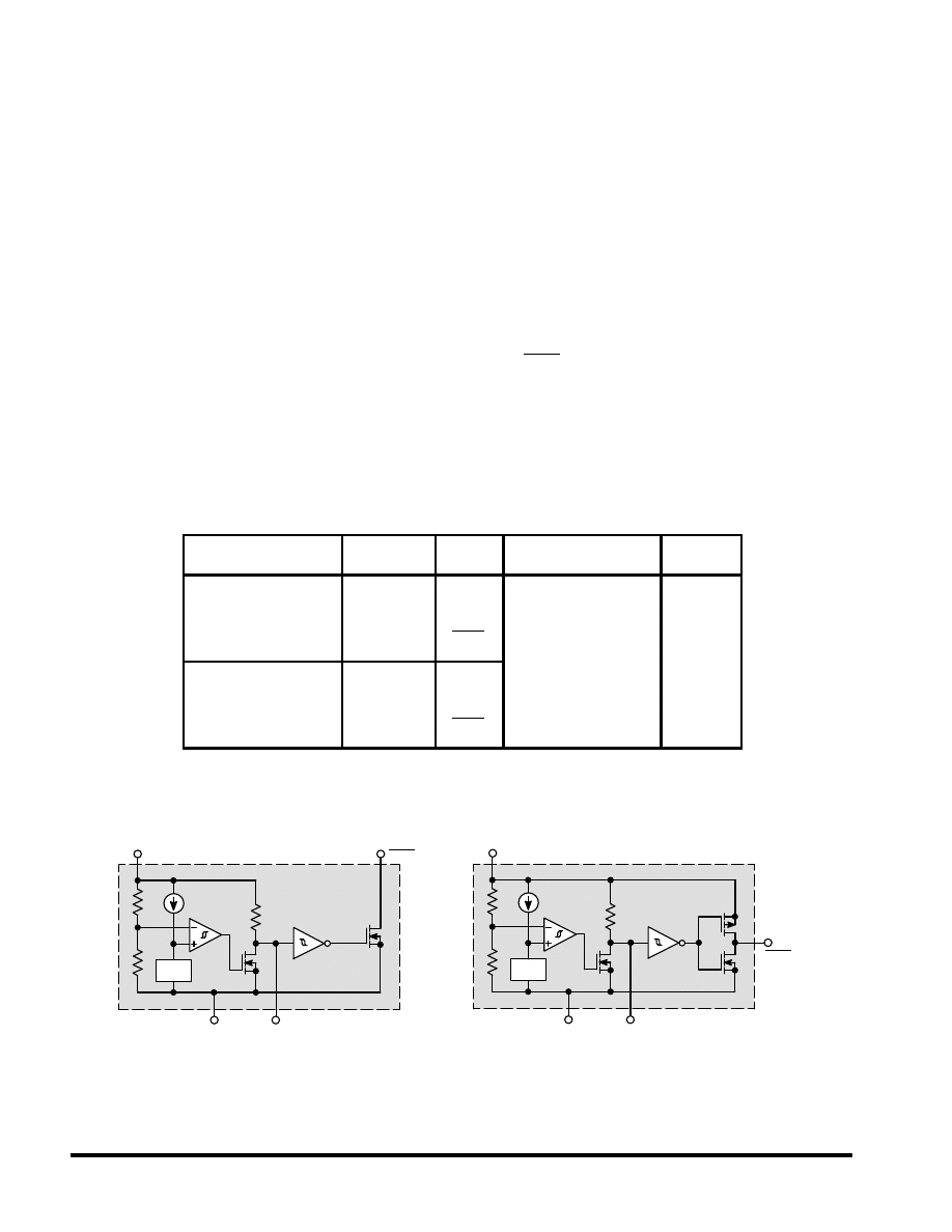
Motorola Master Selection Guide
Analog and Interface Integrated Circuits
4.2–38
Supervisory Circuits
(continued)
Micropower Undervoltage Sensing Circuits with
Programmable Output Delay
MC33465N
TA = –30
°
to +80
°
C, Case 1212
The MC33465 series are micropower undervoltage
sensing circuits that are specifically designed for use with
battery powered microprocessor based systems, where
extended battery life is required. A choice of several threshold
voltages from 0.9 V to 4.5 V are available. This device features
a very low quiescent bias current of 1.0
µ
A typical.
The MC33465 series features a highly accurate voltage
reference, a comparator with precise thresholds and built–in
hysteresis to prevent erratic reset operation, a choice of output
configurations between open drain or complementary, a time
delayed output, which can be programmed by the system
designer, and guaranteed operation below 1.0 V with
extremely low standby current. This device is available in a
SOT–23 5–pin surface mount package.
Applications include direct monitoring of the MPU/logic
power supply used in appliance, automotive, industrial and
portable equipment.
MC33465 Features:
•
Extremely Low Standby Current of 1.0
µ
A at Vin = 3.5 V
•
Wide Input Voltage Range (0.7 V to 10 V)
•
Monitors Power Supply Voltages from 1.1 V to 5.0 V
•
High Accuracy Detector Threshold (
±
2.5%)
•
Two Reset Output Types (Open Drain or Complementary
Drive)
•
Programmable Output Delay by External Capacitor
(100 ms typ. with 0.15
µ
F)
•
Surface Mount Package (SOT–23 5–Pin)
•
Convenient Tape and Reel (3000 per Reel)
ORDERING INFORMATION
Device
Threshold
Voltage
Type
Operating
Temperature Range
Package
MC33465N–09ATR
0.9
O
T
30
°
80
°
C
SOT 23
MC33465N–20ATR
2.0
Open
T
30
°
80
°
C
SOT 23
MC33465N–27ATR
2.7
Drain
T
30
°
80
°
C
SOT 23
MC33465N–30ATR
3.0
Reset
T
30
°
80
°
C
SOT 23
MC33465N–45ATR
4.5
Reset
TA = –30
°
to +80
°
C
SOT–23
MC33465N–09CTR
0.9
C
l
TA = –30
°
to +80
°
C
SOT–23
MC33465N–20CTR
2.0
Compl.
MC33465N–27CTR
2.7
MOS
MC33465N–30CTR
3.0
Reset
MC33465N–45CTR
4.5
Reset
Other voltages from 0.9 to 6.0 V, in 0.1 V increments, are available. Consult factory for information.
MC33465N–YYATR
Open Drain Output Configuration
MC33465N–YYCTR
Complementary Output Configuration
YY Denotes Threshold Voltage
Vref
2
Input
1
Reset
3
Gnd
5
CD
RD
Vref
2
Input
3
Gnd
5
CD
RD
1
Reset

Motorola Master Selection Guide
Analog and Interface Integrated Circuits
4.2–39
Supervisory Circuits
(continued)
Undervoltage Sensing Circuit
MC34064P–5, D–5, DM–5
TA = 0
°
to +70
°
C, Case 29, 751, 846A
MC33064P–5, D–5, DM–5
TA = –40
°
to +85
°
C, Case 29, 751, 846A
MC34164P–3, P–5, D–3, D–5, DM–3, DM–5
TA = 0
°
to +70
°
C, Case 29, 751, 846A
MC33164P–3, P–5, D–3, D–5, DM–3, DM–5
TA = –40
°
to +85
°
C, Case 29, 751, 846A
The MC34064 and MC34164 are two families of
undervoltage sensing circuits specifically designed for use as
reset controllers in microprocessor–based systems. They
offer the designer an economical solution for low voltage
detection with a single external resistor. Both parts feature a
trimmed bandgap reference, and a comparator with precise
thresholds and built–in hysteresis to prevent erratic reset
operation.
The two families of undervoltage sensing circuits taken
together, cover the needs of the most commonly specified
power supplies used in MCU/MPU systems. Key parameter
specifications of the MC34164 family were chosen to
complement the MC34064 series. The table summarizes
critical parameters of both families. The MC34064 fulfills the
needs of a 5.0 V
±
5% system and features a tighter hysteresis
specification. The MC34164 series covers 5.0 V
±
10% and
1 (1)
Input
2 (2)
Gnd
3 (4)
Reset
1.2 Vref
Pin numbers in
parenthesis
are for the
D suffix package.
3.0 V
±
5% power supplies with significantly lower power
consumption, making them ideal for applications where
extended battery life is required such as consumer products
or hand held equipment.
Applications include direct monitoring of the 5.0 V MPU/
logic power supply used in appliance, automotive, consumer,
and industrial equipment.
The MC34164 is specifically designed for battery powered
applications where low bias current (1/25th of the MC34064’s)
is an important characteristic.
Table 14. Undervoltage Sense/Reset Controller Features
MC34X64 devices are specified to operate from 0
°
to +70
°
C, and MC33X64 devices operate from –40
°
to +85
°
C.
D
i
Standard
Power
Typical
Threshold
Typical
Hysteresis
Minimum
Output
Power
Supply
Input
Maximum
Quiescent
S ffi /
Device
Power
Supply
Supported
Threshold
Voltage
(V)
Hysteresis
Voltage
(V)
Output
Sink
Current (mA)
Input
Voltage
Range (V)
Quiescent
Input
Current
Suffix/
Package
MC34064/MC33064
5.0 V
±
5%
4.6
0.02
10
1.0 to 10
500
µ
A
@
P–5/29
@
Vin = 5.0 V
D–5/751
Vin = 5.0 V
DM–5/846A
MC34164/MC33164
5.0 V
±
10%
4.3
0.09
7.0
1.0 to 12
20
µ
A
@
P–5/29
@
Vin = 5.0 V
D–5/751
Vin = 5.0 V
DM–5/846A
MC34164/MC33164
3.0 V
±
5%
2.7
0.06
6.0
1.0 to 12
15
µ
A
@
P–3/29
@
Vin = 3.0 V
D–3/751
Vin = 3.0 V
DM–3/846A

Motorola Master Selection Guide
Analog and Interface Integrated Circuits
4.2–40
Supervisory Circuits
(continued)
Universal Voltage Monitor
MC34161P, D
TA = 0
°
to +70
°
C, Case 626, 751
MC33161P, D
TA = –40
°
to +85
°
C, Case 626, 751
The MC34161, MC33161 series are universal voltage
monitors intended for use in a wide variety of voltage sensing
applications. These devices offer the circuit designer an
economical solution for positive and negative voltage
detection. The circuit consists of two comparator channels
each with hysteresis, a unique Mode Select Input for channel
programming, a pinned out 2.54 V reference, and two open
collector outputs capable of sinking in excess of 10 mA. Each
comparator channel can be configured as either inverting or
noninverting by the Mode Select Input. This allows over,
under, and window detection of positive and negative
voltages. The minimum supply voltage needed for these
devices to be fully functional is 2.0 V for positive voltage
sensing and 4.0 V for negative voltage sensing.
Applications include direct monitoring of positive and
negative voltages used in appliance, automotive, consumer,
and industrial equipment.
•
Unique Mode Select Input Allows Channel Programming
•
Over, Under, and Window Voltage Detection
•
Positive and Negative Voltage Detection
•
Fully Functional at 2.0 V for Positive Voltage Sensing and
4.0 V for Negative Voltage Sensing
•
Pinned Out 2.54 V Reference with Current Limit Protection
•
Low Standby Current
•
Open Collector Outputs for Enhanced Device Flexibility
2.54 V
Reference
Channel 1
Channel 2
2.8 V
1.27 V
0.6 V
1.27 V
Vref
Gnd
VCC
Mode
Select
Input 1
Input 2
Output 1
Output 2
1
2
3
4
5
6
7
8
TRUTH TABLE
Mode Select
Pin 7
Input 1
Pin 2
Output 1
Pin 6
Input 2
Pin 3
Output 2
Pin 5
Comments
GND
0
1
0
1
0
1
0
1
Channels 1 & 2: Noninverting
Vref
0
1
0
1
0
1
1
0
Channel 1: Noninverting
Channel 2: Inverting
VCC (>2.0 V)
0
1
1
0
0
1
1
0
Channels 1 & 2: Inverting
POSITIVE AND NEGATIVE OVERVOLTAGE DETECTOR
+
1.27 V
+
1.27 V
+
2.8 V
+
0.6 V
+
–
2.54 V
Reference
–
+
–
+
+
–
4
1
7
2
3
5
6
R4
R3
–VS1
VS2
R1
R2
8
VCC
Output
Voltage
Pins 5, 6
Gnd
LED “On”
VHys2
VHys1
VCC
Gnd
Input –VS1
V4
V3
V1
V2
Input VS2
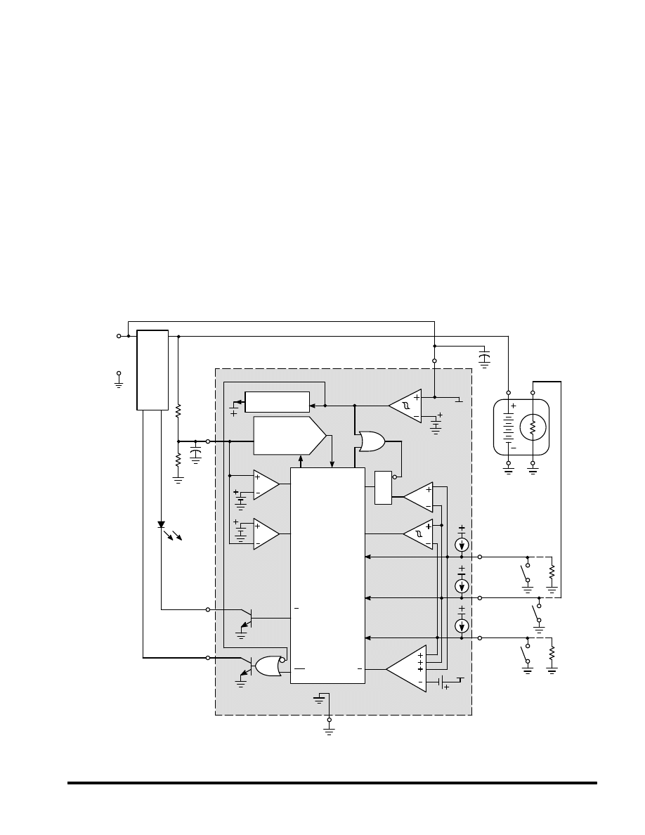
Motorola Master Selection Guide
Analog and Interface Integrated Circuits
4.2–41
Battery Management Circuits
Battery Charger ICs
Battery Fast Charge Controller
MC33340P, D
TA = –25
°
to +85
°
C, Case 626, 751
The MC33340 is a monolithic control IC that is specifically
designed as a fast charge controller for Nickel Cadmium
(NiCd) and Nickel Metal Hydride (NiMH) batteries. This
device features negative slope voltage detection as the pri-
mary means for fast charge termination. Accurate detection
is ensured by an output that momentarily interrupts the
charge current for precise voltage sampling. An additional
secondary backup termination method can be selected that
consists of either a programmable time or temperature limit.
Protective features include battery over and undervoltage
detection, latched over temperature detection, and power
supply input undervoltage lockout with hysteresis. Provisions
for entering a rapid test mode are available to enhance end
product testing. This device is available in an economical
8–lead surface mount package.
•
Negative Slope Voltage Detection with 4.0 mV Sensitivity
•
Accurate Zero Current Battery Voltage Sensing
•
High Noise Immunity with Synchronous VFC/Logic
•
Programmable 1 to 4 Hour Fast Charge Time Limit
•
Programmable Over/Under Temperature Detection
•
Battery Over and Undervoltage Fast Charge Protection
•
Rapid System Test Mode
•
Power Supply Input Undervoltage Lockout with
Hysteresis
•
Operating Voltage Range of 3.0 V to 18 V
Battery
Detect
DC
Input
VCC
Undervoltage
Lockout
Over
Temp
Latch
Temp
Detect
Time/
Temp
Select
Vsen
Vsen
Gate
Fast/
Trickle
Voltage to
Frequency
Converter
–
∆
V Detect
Counter
Timer
Battery
Pack
Internal Bias
VCC
VCC
Gnd
Q
R
S
t1/Tref High
t2/Tsen
t3/Tref Low
7
6
5
8
4
3
2
1
High
Low
Vsen
Gate
F/T
Over
Under
t1
t2
t3
t/T
Ck
F/V
R
Regulator
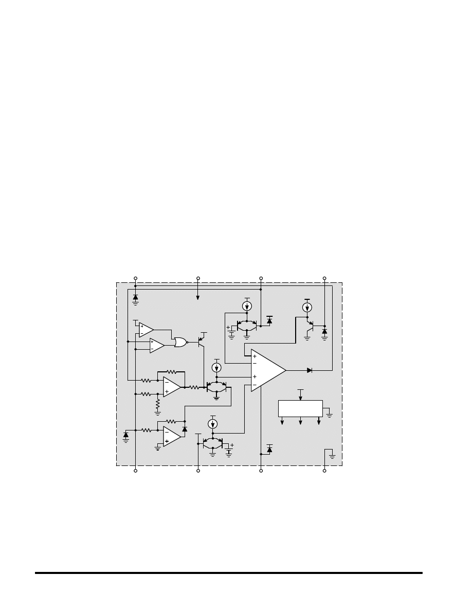
Motorola Master Selection Guide
Analog and Interface Integrated Circuits
4.2–42
Battery Charger ICs
(continued)
Power Supply
Battery Charger
Regulation Control Circuit
MC33341P, D
TA = –25
°
to +85
°
C, Case 626, 751
The MC33341 is a monolithic regulation control circuit that
is specifically designed to close the voltage and current
feedback loops in power supply and battery charger
applications. This device features the unique ability to perform
source high–side, load high–side, source low–side, and load
low–side current sensing, each with either an internally fixed
or externally adjustable threshold. The various current
sensing modes are accomplished by a means of selectively
using the internal differential amplifier, inverting amplifier, or a
direct input path. Positive voltage sensing is performed by an
internal voltage amplifier. The voltage amplifier threshold is
internally fixed and can be externally adjusted in all low–side
current sensing applications. An active high drive output is
provided to directly interface with economical optoisolators for
isolated output power systems. This device is available in
8–lead dual–in–line and surface mount packages.
•
Differential Amplifier for High–Side Source and Load
Current Sensing
•
Inverting Amplifier for Source Return Low–Side Current
Sensing
•
Noninverting Input Path for Load Low–Side Current
Sensing
•
Fixed or Adjustable Current Threshold in all Current
Sensing Modes
•
Positive Voltage Sensing in all Current Sensing Modes
•
Fixed Voltage Threshold in all Current Sensing Modes
•
Adjustable Voltage Threshold in all Low–Side Current
Sensing Modes
•
Output Driver Directly Interfaces with Economical
Optoisolators
•
Operating Voltage Range of 2.3 V to 16 V
4
3
2
1
5
6
7
8
Gnd
Compensation
Current
Threshold Adjust
Current Sense
Input A
Current Sense Input B/
Voltage Threshold Adjust
Voltage Sense
Input
VCC
Drive Output
Reference
Differential Amp
Inverting Amp
VCC
VCC
1.2 V
0.4 V
VCC
VCC
VCC
VCC
VCC
VCC
VCC
R
R
R
R
R
R
1.2 V
0.2 V
0.4 V
1.2 V
0.2 V
Differential Amp
Disable Logic
Transconductance
Amp
Vsen
Vth
Isen
Ith
V
I
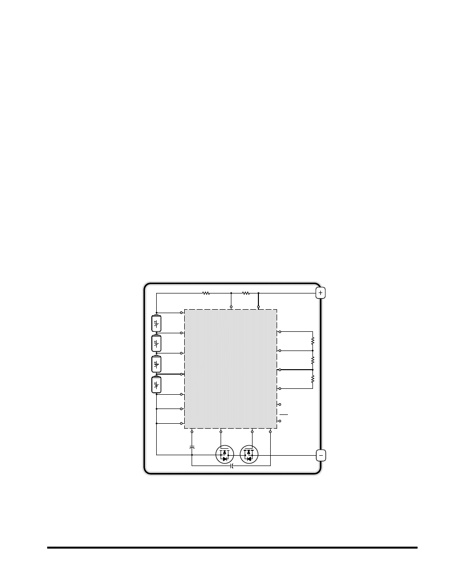
Motorola Master Selection Guide
Analog and Interface Integrated Circuits
4.2–43
Battery Pack ICs
Lithium Battery Protection Circuit for One to Four Cell Battery Packs
MC33345DW, DTB
TA = –25
°
to +85
°
C, Case 751D, 948E
The MC33345 is a monolithic lithium battery protection
circuit that is designed to enhance the useful operating life of
one to four cell rechargeable battery packs. Cell protection
features consist of independently programmable charge and
discharge limits for both voltage and current with a delayed
current shutdown, cell voltage balancing with on–chip
balancing resistors, and a virtually zero current sleepmode
state when the cells are discharged. Additional features
include an on–chip charge pump for reduced MOSFET losses
while charging or discharging a low cell voltage battery pack,
and the programmability for a one to four cell battery pack.
This protection circuit requires a minimum number of external
components and is targeted for inclusion within the battery
pack. The MC33345 is available in standard and low profile 20
lead surface mount packages.
•
Independently Programmable Charge and Discharge
Limits for Both Voltage and Current
•
Charge and Discharge Current Limit Detection with
Delayed Shutdown
•
Cell Voltage Balancing
•
On–Chip Balancing Resistors
•
Virtually Zero Current Sleepmode State when Cells are
Discharged
•
Charge Pump for Reduced Losses with a Low Cell
Voltage Battery Pack
•
Programmable for One, Two, Three or Four Cell
Applications
•
Minimum External Components for Inclusion within the
Battery Pack
•
Available in Low Profile Surface Mount Packages
Charge
Gate Drive
Output
Typical Four Cell Smart Battery Pack
7
Charge
Current Limit
6
Current Sense
Common
Cell 4/VCC/
Discharge
Current Limit
MC33345
Discharge Voltage
Threshold
3
4
5
1
Charge Voltage
Threshold
Cell Voltage
Return
Cell Voltage
Charge Pump
Output
14
Discharge
Gate Drive
Output
13
9
8
Charge
Gate Drive
Common
2
Cell 3
20
Cell 2
19
Cell 1/VC
18
Ground
Program 2
10
17
Fault Output
Program 1
11
16
15
Test Input
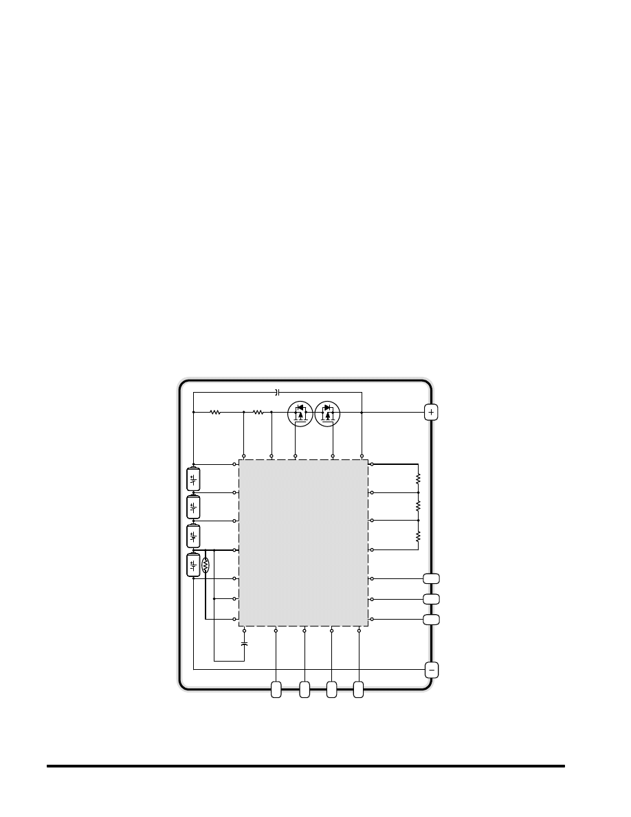
Motorola Master Selection Guide
Analog and Interface Integrated Circuits
4.2–44
Battery Pack ICs
(continued)
Lithium Battery Protection Circuit for Three or Four Cell Battery Packs
MC33346DW, DTB
TA = –40
°
to +85
°
C, Case 751E, 948H
The MC33346 is a monolithic lithium battery protection cir-
cuit that is designed to enhance the useful operating life of
three or four cell rechargeable battery packs. Cell protection
features consist of independently programmable charge and
discharge limits for both voltage and current with a delayed
current shutdown, cell voltage balancing with on–chip bal-
ancing resistors, and virtually zero current sleepmode state
when the cells are discharged. Additional features consists of
a six wire microcontroller interface bus that can selectively
provide a pulse output that represents the internal reference
voltage, cell voltage, cell current and temperature, as well as
control the states of four internal balancing and two external
MOSFET switches. A microcontroller time reference output is
available for gas gauge implementation. This protection cir-
cuit requires a minimum number of external components and
is targeted for inclusion within the battery pack. The
MC33346 is available in standard and low profile 24 lead sur-
face mount packages.
•
Independently Programmable Charge and Discharge
Limits for Both Voltage and Current
•
Delayed Current Shutdown
•
Cell Voltage Balancing with On–Chip Resistors
•
Six Wire Microcontroller Interface Bus
•
Data Output for Reference, Voltage, Current, and
Temperature
•
Microcontroller Time Reference Output for Gas Gauging
•
Virtually Zero Current Sleepmode State when Cells are
Discharged
•
Programmable for Three or Four Cell Applications
•
Minimum External Components for Inclusion within the
Battery Pack
•
Available in Low Profile Surface Mount Packages
Cell
Program
18
VC
Logic
Supply
17
A–to–D
Converter
Period
Typical Four Cell Smart Battery Pack
Charge
Gate Drive
Common
21
Cell 4/VCC/
Discharge
Current Limit
MC33346
Discharge Voltage
Threshold
2
4
5
1
Charge Voltage
Threshold
Cell Voltage
Return
Cell Voltage
9
Charge Gate
Turn Off/
Test Input
3
Cell 3
24
Cell 2
23
Cell 1
22
Ground
Temp
8
19
Reference Clock Output
11
15
16
Data Output
Ref/V/I/T
12
Interrupt Output
10
Data
Input
13
Address
Input
Discharge
Gate Drive
Output
14
Charge
Current
Limit
6
Current
Sense
Common
7
Charge
Gate Drive
Output
20

Motorola Master Selection Guide
Analog and Interface Integrated Circuits
4.2–45
Battery Pack ICs
(continued)
Lithium Battery Protection Circuit for One or Two Cell Battery Packs
MC33347D, DTB
TA = –25
°
to +85
°
C, Case 751B, 948F
The MC33347 is a monolithic lithium battery protection cir-
cuit that is designed to enhance the useful operating life of
one or two cell rechargeable battery packs. Cell protection
features consist of independently programmable charge and
discharge limits for both voltage and current with a delayed
current shutdown, continuous cell voltage balancing with the
choice of on–chip or external balancing resistors, and a virtu-
ally zero current sleepmode state when the cells are dis-
charged. Additional features include an on–chip charge
pump for reduced MOSFET losses while charging or dis-
charging a low cell voltage battery pack, and the programma-
bility for one or two cell battery pack. This protection circuit
requires a minimum number of external components and is
targeted for inclusion within the battery pack. This MC33347
is available in standard and low profile 16 lead surface mount
packages.
•
Independently Programmable Charge and Discharge
Limits for Both Voltage and Current
•
Charge and Discharge Current Limit Detection with
Delayed Shutdown
•
Continuous Cell Voltage Balancing
•
On–Chip or External Balancing Resistors
•
Virtually Zero Current Sleepmode State when Cells are
Discharged
•
Charge Pump for Reduced Losses with a Low Cell
Voltage Battery Pack
•
Programmable for One or Two Cell Applications
•
Minimum External Components for Inclusion within the
Battery Pack
•
Available in Low Profile Surface Mount Packages
Discharge
Gate Drive
Output
Cell Program/
Test
VCC/
Overcharge
Current Limit
Typical Two Cell Smart Battery Pack
Discharge Voltage
Threshold
Charge Pump
Output
15
Charge
Gate Drive
Output
14
12 11
Charge
Gate Drive
Common
10
9
Current Sense
Common
13
4
2
3
1
16
Balance 2
Balance 1
Ground
VCell 1
6
7
8
5
Charge Voltage
Threshold
Cell Voltage
Return
Cell Voltage
MC33347
VCell2/
Discharge
Current Limit

Motorola Master Selection Guide
Analog and Interface Integrated Circuits
4.2–46
Battery Pack ICs
(continued)
Lithium Battery Protection Circuit for One Cell Battery Packs
MC33348D
TA = –25
°
to +85
°
C, Case 751
The MC33348 is a monolithic lithium battery protection cir-
cuit that is designed to enhance the useful operating life of a
one cell rechargeable battery pack. Cell protection features a
consist of internally trimmed charge and discharge voltage
limits, discharge current limit detection with a delayed shut-
down, and a virtually zero current sleepmode state when the
cell is discharged. An additional feature includes an on–chip
charge pump for reduced MOSFET losses while charging or
discharging a low cell voltage battery pack. This protection
circuit requires a minimum number of external components
and is targeted for inclusion within the battery pack. This
MC33348 is available in a standard 8 lead surface mount
package.
•
Internally Trimmed Charge and Discharge Voltage Limits
•
Discharge Current Limit Detection with Delayed
Shutdown
•
Virtually Zero Current Sleepmode State when Cells are
Discharged
•
Charge Pump for Reduced Losses with a Low Cell
Voltage Battery Pack
•
Dedicated for One Cell Applications
•
Minimum Components for Inclusion within the Battery
Pack
•
Available in Standard 8 Lead Surface Mount Package
Typical One Cell Smart Battery Pack
VCC
Charge Pump
Output
8
Charge
Gate Drive
Output
Discharge
Gate Drive
Output
4
6
5
Charge
Gate Drive
Common/
Discharge
Current Limit
7
1
3
2
Ground
Test
MC33348
Cell
Voltage
ORDERING INFORMATION
Device
Charge
Overvoltage
Threshold (V)
Charge
Overvoltage
Hysteresis (mV)
Discharge
Undervoltage
Threshold (V)
Discharge
Current Limit
Threshold (mV)
Operating
Temperature Range
Package
MC33348D–1
4.20
300
2.25
400
T
25
°
85
°
C
SO 8
MC33348D–2
300
200
T
25
°
85
°
C
SO 8
MC33348D–3
4.25
300
2.28
400
TA = –25
°
to +85
°
C
SO–8
MC33348D–4
300
200
TA = –25
°
to +85
°
C
SO–8
MC33348D–5
4.35
2.30
400
MC33348D–6
200
NOTE:
Additional threshold limit options can be made available. Consult factory for information.
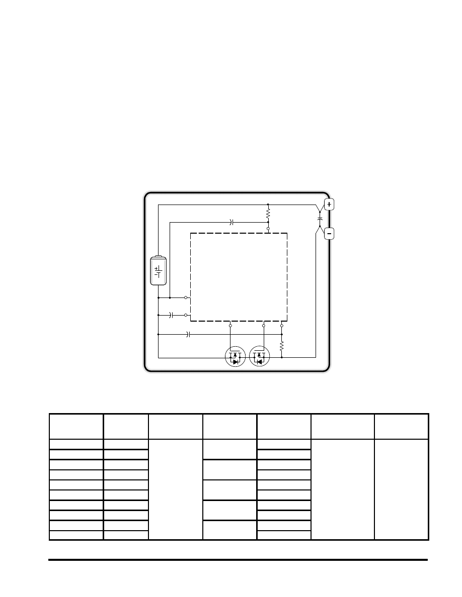
Motorola Master Selection Guide
Analog and Interface Integrated Circuits
4.2–47
Battery Pack ICs
(continued)
Lithium Battery Protection Circuit for One Cell Battery Packs
MC33349
TA = –40
°
to 85
°
C, Case 1262
The MC33349 is a monolithic lithium battery protection cir-
cuit that is designed to enhance the useful operating life of a
one cell rechargeable battery pack. Cell protection features
consist of internally trimmed charge and discharge voltage
limits, charge and discharge current limit detection, and a
virtually zero current sleepmode state when the cell is dis-
charged. This protection circuit requires a minimum number
of external components and is targeted for inclusion within
the battery pack. This MC33349 is available in SOT–23
6 lead surface mount package.
•
Internally Trimmed Charge and Discharge Voltage Limits
•
Charge and Discharge Current Limit Detection
•
Virtually Zero Current Sleepmode State when Cells are
Discharged
•
Dedicated for One Cell Applications
•
Minimum Components for Inclusion within the Battery
Pack
•
Available in a Low Profile Surface Mount Package
Typical One Cell Smart Battery Pack
This device contains 264 active transistors.
1
3
2
5
6
4
MC33349
0.1
µ
F
0.1
µ
F
0.01
µ
F
100
Ω
1.0 k
Ω
ORDERING INFORMATION
Device
Charge
Overvoltage
Threshold (V)
Charge
Overvoltage
Hysteresis (mV)
Discharge
Undervoltage
Threshold (V)
Current Limit
Threshold (mV)
Operating
Temperature Range
Package
MC33349N–1
4.2
200
2 28
150
T
40
°
85
°
C
SOT 23
MC33349N–2
4.2
200
2.28
75
T
40
°
85
°
C
SOT 23
MC33349N–3
4.25
200
2 28
150
T
40
°
85
°
C
SOT 23
MC33349N–4
4.25
200
2.28
75
T
40
°
85
°
C
SOT 23
MC33349N–5
4.3
200
2 29
150
TA = –40
°
to 85
°
C
SOT–23
MC33349N–6
4.3
200
2.29
75
TA = –40
°
to 85
°
C
(6 Lead)
MC33349N–7
4.35
2 30
150
MC33349N–8
4.35
2.30
75
MC33349N–9
4.65
2 35
150
MC33349N–10
4.65
2.35
75
Motorola Master Selection Guide
Analog and Interface Integrated Circuits
4.2–48
Power Supply and Management IC for Handheld
Electronic Products
MC34280
0
°
C to +70
°
C, Case 873A
The MC34280 is a power supply integrated circuit which
provides two boost regulated outputs and some power man-
agement supervisory functions. Both regulators apply Pulse–
Frequency–Modulation (PFM). The main step–up regulator
output can be externally adjusted from 2.7V to 5V. An internal
synchronous rectifier is used to ensure high efficiency
(achieve 87%). The auxiliary regulator with a built–in power
transistor can be configured to produce a wide range of posi-
tive voltage (can be used for LCD contrast voltage). This volt-
age can be adjusted from +5V to +25V by an external poten-
tiometer; or by a microprocessor, digitally through a 6–bit
internal DAC.
The MC34280 has been designed for battery powered
hand–held products. With the low start–up voltage from 1V
and the low quiescent current (typical 35
µ
A); the MC34280
is best suited to operate from 1 to 2 AA/ AAA cell. Moreover,
supervisory functions such as low battery detection, CPU
power–on reset, and back–up battery control, are also
included in the chip. It makes the MC34280 the best one–
chip power management solution for applications such as
electronic organizers and PDAs.
•
Low Input Voltage, 1V up
•
Low Quiescent Current in Standby Mode: 35
µ
A typical
•
PFM and Synchronous Rectification to ensure high
efficiency (87% @200mA Load)
•
Adjustable Main Output: nominal 3.3V @ 200mA max,
with 1.8V input
•
Auxiliary Output Voltage can be digitally controlled by
microprocessor
•
Auxiliary Output Voltage:
+5V @ 25mA max, with 1.8V input
+25V @ 15mA max, with 1.8V input
•
Current Limit Protection
•
Power–ON Reset Signal with Programmable Delay
•
Battery Low Detection
•
Lithium Battery Back–up
•
32–Pin LQFP Package
ORDERING INFORMATION
Device
Operating
Temperature Range
Package
MC34280
0
°
C to +70
°
C
32–pin LQFP

Motorola Master Selection Guide
Analog and Interface Integrated Circuits
4.2–49
Power Supply and Management IC for Handheld Electronic Products
(continued)
Power
ON
Reset
Lithium
Battery
Backup
Voltage
Reference
Low
Battery
Detect
Current
Bias
Control and
Gate Drive
Startup
Current
Limit
Main Regulator with
Synchronous Rectifier
LIBATCL
LIBATON
LOWBATB
PORB
DGND
LOWBATSEN
14
13
12
11
10
9
GND
GND
RLBb
r = 900 k
RLBa
r = 300 k
LIBATIN
27
28
29
30
31
32
GND
N/C
LIBATOUT
VMAINGND
VMAINSW
1N5817
M2
M1
IREF
AGND
8
7
VREF
VBAT
GND
RMAINb
r = 1000 k
CMAINb
c = 100p
VBAT
VMAIN
PDELAY
VDD
VDD
VMAINFB
VBAT
6
5
4
VREF
GND
GND
Ren
r = 1000 k
VBAT
Battery
Lock
Switch
VMAIN
GND
CVDD
c = 20u
3
2
1
ENABLE
Riref
r = 480 k
R123
r = 5
CMAIN
c = 100u
10 V SMT
tantalum
LMAIN
L = 33u
(Rs < 60 mOhm)
GND
Optional
CMAINbp
c = 100u
10 V SMT
tantalum
M3
d
s
d
s
d
s
GND
GND
Typical Application Block Diagram
Cpor
c = 80n
VAUXADJ
15
VAUXCON
16
VAUXEN
17
VBAT
LIBATCL
LIBATON
LOWBAT
PORB
VAUXADJ
VAUXCON
VAUXEN
VAUXFBP
GND
Optional
CAUXbp
c = 100u
10 V SMT
tantalum
VBAT
18
20
21
19
22
23
24
Level
Control
Current
Limit
Auxiliary Regulator
Control and
Base Drive
LAUX
L = 22u
(Rs < 60 mOhm)
VAUXFBN
GND
Caux
c = 30u
30 V SMT
tantalum
VAUX
1N5818
GND
GND
VAUXREF
(1.1 V to 2.2 V)
VAUXBDV
VAUXCHG
VAUXBASE
N/C
Rauxb
r = 2.2 M
Rauxa
r = 200 k
GND
CAUXb
c = 2n
CAUXa
c = 33n
Q1
VAUXEMR
26
VAUXSW
25
Optional
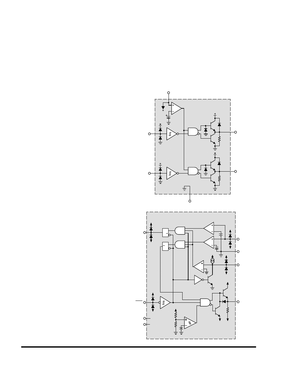
Motorola Master Selection Guide
Analog and Interface Integrated Circuits
4.2–50
MOSFET/IGBT Drivers
High Speed Dual Drivers
(Inverting)
MC34151P, D
TA = 0
°
to +70
°
C, Case 626, 751
MC33151P, D
TA = –40
°
to +85
°
C, Case 626, 751
(Noninverting)
MC34152P, D
TA = 0
°
to +70
°
C, Case 626, 751
MC33152P, D
TA = –40
°
to +85
°
C, Case 626, 751
These two series of high speed dual MOSFET driver ICs
are specifically designed for applications requiring low current
digital circuitry to drive large capacitive loads at high slew
rates. Both series feature a unique undervoltage lockout
function which puts the outputs in a defined low state in an
undervoltage condition. In addition, the low “on” state
resistance of these bipolar drivers allows significantly higher
output currents at lower supply voltages than with competing
drivers using CMOS technology.
The MC34151 series is pin–compatible with the MMH0026
and DS0026 dual MOS clock drivers, and can be used as
drop–in replacements to upgrade system performance. The
MC34152 noninverting series is a mirror image of the inverting
MC34151 series.
These devices can enhance the drive capabilities of first
generation switching regulators or systems designed with
CMOS/TTL logic devices. They can be used in dc–to–dc
converters, motor controllers, capacitor charge pump
converters, or virtually any other application requiring high
speed operation of power MOSFETs.
Single IGBT Driver
MC33153P, D
TA = –40
°
to +105
°
C, Case 626, 751
The MC33153 is specifically designed to drive the gate of
an IGBT used for ac induction motors. It can be used with
discrete IGBTs and IBGT modules up to 100 A.
Typical applications are ac induction motor control,
brushless dc motor control, and uninterruptable power
supplies.
These devices are available in dual–in–line and surface
mount packages and include the following features:
•
High Current Output Stage : 1.0 A Source – 2.0 A Sink
•
Protection Circuits for Both Conventional and
SenseIGBTs
•
Current Source for Blanking Timing
•
Protection Against Overcurrent and Short Circuit
•
Undervoltage Lockout Optimized for IGBT’s
•
Negative Gate Drive Capability
MC34151
3
Logic
Input A
Logic
Input B
2
4
Gnd
Drive
Output A
Drive
Output B
5
7
6
100 k
100 k
5.7 V
VCC
Current
Sense
Input
1
2
Kelvin
Gnd
8
Blanking
Desatur–
ation
5
Gate
Drive
Ouptut
7
4
3
6
VCC
VEE
Input
Output
VCC
VEE
VCC
Desat./Blank.
Comparator
Overcurrent
Comparator
Over–
current
Latch
S
R
Q
VCC
VEE
VCC
VEE
VCC
VEE
VEE VEE
VCC
VCC
Short Circuit
Comparator
S
R
Q

Motorola Master Selection Guide
Analog and Interface Integrated Circuits
4.2–51
MOSFET/IGBT Drivers
(continued)
Single IGBT Gate Driver
MC33154D, P
TA = –40
°
to +85
°
C, Case 626, 751
The MC33154 is specifically designed as an IGBT driver
for high power applications including ac induction motor con-
trol, brushless dc motor control and uninterruptible power
supplies.
The MC33154 is similar to the MC33153, except that the
output drive is in–phase with the logic input, the output
source current drive is four times higher and the supply volt-
age rating is higher.
Although designed for driving discrete and module IGBTs,
this device offers a cost effective solution for driving power
MOSFETs and Bipolar Transistors.
These devices are available in dual–in–line and surface
mount packages and include the following features:
•
High Current Output Stage: 4.0 A Source/2.0 A Sink
•
Protection Circuits for Both Conventional and Sense
IGBTs
•
Programmable Fault Blanking Time
•
Protection against Overcurrent and Short Circuit
•
Undervoltage Lockout Optimzed for IGBTs
•
Negative Gate Drive Capability
•
Cost Effectively Drives Power MOSFETs and Bipolar
Transistors
Short Circuit
Latch
Overcurrent
Latch
Fault
Output
S
Q
R
Current
Sense
Input
Kelvin
Gnd
Fault
Blanking/
Desaturation
Input
Gate
Drive
Output
Short Circuit
Comparator
Overcurrent
Comparator
Desat/Blank
Comparator
Under
Voltage
Lockout
Input
VEE
VCC
VCC
VCC
VEE
VEE
VCC
VEE
VCC
VEE
VCC
VEE
VCC
S
Q
R
VCC
7
4
5
8
2
1
130 mV
65 mV
1.0 mA
6.5 V
Output
Stage
12 V/
11 V
VCC
6
VEE
3
Motorola Master Selection Guide
Analog and Interface Integrated Circuits
4.2–52
Power Supply Circuits Package Overview
CASE 707
N SUFFIX
CASE 29
P, Z SUFFIX
CASE 221A
T SUFFIX
CASE 314D
T SUFFIX
CASE 646
P SUFFIX
CASE 369A
DT SUFFIX
CASE 648E
P SUFFIX
CASE 314B
TV SUFFIX
CASE 314A
TH SUFFIX
CASE 369
DT–1 SUFFIX
CASE 626
N, P, P1 SUFFIX
CASE 751D
DW SUFFIX
CASES 648, 648C
N, P, P2 SUFFIX
CASE 751A
D SUFFIX
CASE 751G
DW SUFFIX
CASE 751K
D SUFFIX
CASE 751B
D SUFFIX
CASE 751
D, D1, D2 SUFFIX
CASE 751E
DW SUFFIX
CASE 318E
ST SUFFIX
Motorola Master Selection Guide
Analog and Interface Integrated Circuits
4.2–53
Power Supply Circuits Package Overview
(continued)
CASE 936A
D2T SUFFIX
CASE 948E
DTB SUFFIX
CASE 948F
DTB SUFFIX
CASE 948G
DTB SUFFIX
CASE 948H
DTB SUFFIX
CASE 1212
N SUFFIX
CASE 1213
H SUFFIX
CASE 775
FN SUFFIX
CASE 873A
FB SUFFIX
CASE 936
D2T SUFFIX
CASE 846A
DM SUFFIX
CASE 751N
DW SUFFIX

Motorola Master Selection Guide
Analog and Interface Integrated Circuits
4.2–54
Wyszukiwarka
Podobne podstrony:
0 50V 2A LM10C, 0 50V 2A Bench power supply circuit diagrams, schematics, electronic projects
Low Voltage Power Supply Circuits
Convert Computer ATX Power Supply to Lab Power Supply
Jvc Power Supply Description And Trouble Shooting Procedure
Battery Inverter For Modularly Structured Pv Power Supply Systems
(Wydruk – ATX Switching Power Supply 13,8 V Proste zmiany w celu zwiększenia napięcia wyjściowego Ja
Alarm Power Supply L78Sxx id 61 Nieznany (2)
3 2 Lab Install Power Supply
HY3010 power supply, Elektronika, Zasilacze, Zasilacz HY3010, Zasilacz HY3010, HY3010 ,INSTRUKCJA
Lekturki Power Supply Unit Lekturka
How to Modify an ATX Computer Power Supply
Adaptive fuzzy control for uninterruptible power supply with three phase PWM inverter
Control and Power Supply for Resistance Spot Welding (RSW)
Performance Improvements in an arc welding power supply based on resonant inverters (1)
Convert Computer ATX Power Supply to Lab Power Supply
(ebook free energy) 50000 vdc power supply
(ebook electronics) Schematics Power Regulated Power Supply for CB & Ham Radio
Sovereign XS Power Supply Schematic
03a E46 Power Supply and Bus Systems
więcej podobnych podstron