
LETTERS
Detection of individual gas molecules
adsorbed on graphene
F. SCHEDIN
1
, A. K. GEIM
1
, S. V. MOROZOV
2
, E. W. HILL
1
, P. BLAKE
1
, M. I. KATSNELSON
3
AND K. S. NOVOSELOV
1
*
1
Manchester Centre for Mesoscience and Nanotechnology, University of Manchester, Manchester, M13 9PL, UK
2
Institute for Microelectronics Technology, 142432 Chernogolovka, Russia
3
Institute for Molecules and Materials, University of Nijmegen, 6525 ED Nijmegen, Netherlands
*
e-mail: Konstantin.Novoselov@manchester.ac.uk
Published online: 29 July 2007; doi:10.1038/nmat1967
The ultimate aim of any detection method is to achieve such
a level of sensitivity that individual quanta of a measured
entity can be resolved. In the case of chemical sensors, the
quantum is one atom or molecule. Such resolution has so far
been beyond the reach of any detection technique, including
solid-state gas sensors hailed for their exceptional sensitivity
.
The fundamental reason limiting the resolution of such sensors
is fluctuations due to thermal motion of charges and defects
,
which lead to intrinsic noise exceeding the sought-after signal
from individual molecules, usually by many orders of magnitude.
Here, we show that micrometre-size sensors made from graphene
are capable of detecting individual events when a gas molecule
attaches to or detaches from graphene’s surface. The adsorbed
molecules change the local carrier concentration in graphene one
by one electron, which leads to step-like changes in resistance.
The achieved sensitivity is due to the fact that graphene is an
exceptionally low-noise material electronically, which makes it
a promising candidate not only for chemical detectors but also
for other applications where local probes sensitive to external
charge, magnetic field or mechanical strain are required.
Solid-state gas sensors are renowned for their high sensitivity,
which—in combination with low production costs and miniature
sizes—have made them ubiquitous and widely used in many
applications
. Recently, a new generation of gas sensors has
been demonstrated using carbon nanotubes and semiconductor
nanowires (see, for example, refs 3,4). The high acclaim received
by the latter materials is, to a large extent, due to their exceptional
sensitivity allowing detection of toxic gases in concentrations
as small as 1 part per billion (p.p.b.). This and even higher
levels of sensitivity are sought for industrial, environmental and
military monitoring.
The operational principle of graphene devices described below
is based on changes in their electrical conductivity,
σ
, due to gas
molecules adsorbed on graphene’s surface and acting as donors
or acceptors, similar to other solid-state sensors
. However, the
following characteristics of graphene make it possible to increase
the sensitivity to its ultimate limit and detect individual dopants.
First, graphene is a strictly two-dimensional material and, as
such, has its whole volume exposed to surface adsorbates, which
maximizes their effect. Second, graphene is highly conductive,
exhibiting metallic conductivity and, hence, low Johnson noise even
in the limit of no charge carriers
, where a few extra electrons
can cause notable relative changes in carrier concentration,
n
.
Third, graphene has few crystal defects
, which ensures a low
level of excess
(
1
/f )
noise caused by their thermal switching
.
Fourth, graphene allows four-probe measurements on a single-
crystal device with electrical contacts that are ohmic and have
low resistance. All of these features contribute to make a unique
combination that maximizes the signal-to-noise ratio to a level
sufficient for detecting changes in a local concentration by less than
one electron charge,
e
, at room temperature.
The
studied
graphene
devices
were
prepared
by
micromechanical cleavage of graphite at the surface of oxidized
Si wafers
. This allowed us to obtain graphene monocrystals of
typically 10
µ
m in size. By using electron-beam lithography, we
made electrical (Au/Ti) contacts to graphene and then defined
multiterminal Hall bars by etching graphene in an oxygen
plasma. The microfabricated devices (Fig. 1a, upper inset) were
placed in a variable temperature insert inside a superconducting
magnet and characterized by using field-effect measurements
at temperatures,
T
, from 4 to 400 K and in magnetic fields,
B
,
up to 12 T. This allowed us to find the mobility,
µ
, of charge
carriers (typically,
≈
5,000 cm
2
V
−
1
s
−
1
) and distinguish between
single-, bi- and few-layer devices, in addition to complementary
measurements of their thickness carried out by optical and atomic
force microscopy
. Figure 1a, lower inset, shows an example
of the field-effect behaviour exhibited by our devices at room
temperature. This plot shows that longitudinal (
ρ
xx
) and Hall
(
ρ
xy
) resistivities are symmetric and antisymmetric functions
of gate voltage,
V
g
, respectively.
ρ
xx
exhibits a peak at zero
V
g
,
whereas
ρ
xy
simultaneously passes through zero, which shows that
the transition from electron to hole transport occurs at zero
V
g
indicating that graphene is in its pristine undoped state
.
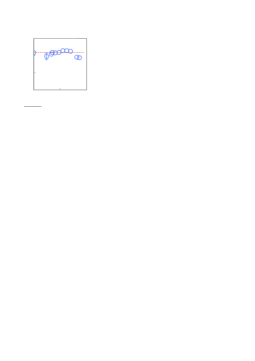
To assess the effect of gaseous chemicals on graphene devices,
the insert was evacuated and then connected to a relatively large
(5 l) glass volume containing a selected chemical strongly diluted
in pure helium or nitrogen at atmospheric pressure. Figure 1b
shows the response of zero-field resistivity,
ρ = ρ
xx
(B =
0
) =
1
/σ
,
to NO
2
, NH
3
, H
2
O and CO in concentrations,
C
, of 1 part per
million (p.p.m.). Large easily detectable changes that occurred
within 1 min and, for the case of NO
2
, practically immediately after
letting the chemicals in can be seen. The initial rapid response
was followed by a region of saturation, in which the resistivity
changed relatively slowly. We attribute this region to redistribution
652
nature
materials
VOL 6 SEPTEMBER 2007 www.nature.com/naturematerials
©
2007
Nature Publishing Group
LETTERS
0.1
1
C (p.p.m.)
Δ
n
(10
10
cm
–2
)
10
1
2
5
10
20
50
–20
0
V
g
(V)
0
2
4
20
and
xy
(k
Ω
)
ρ
ρ
ρ
ρρ
ρ
~ ~
0
500
1,000
–4
–2
0
2
4
t (s)
Δ
/
(%)
I
II
III
IV
NH
3
CO
H
2
O
NO
2
a
b
xy
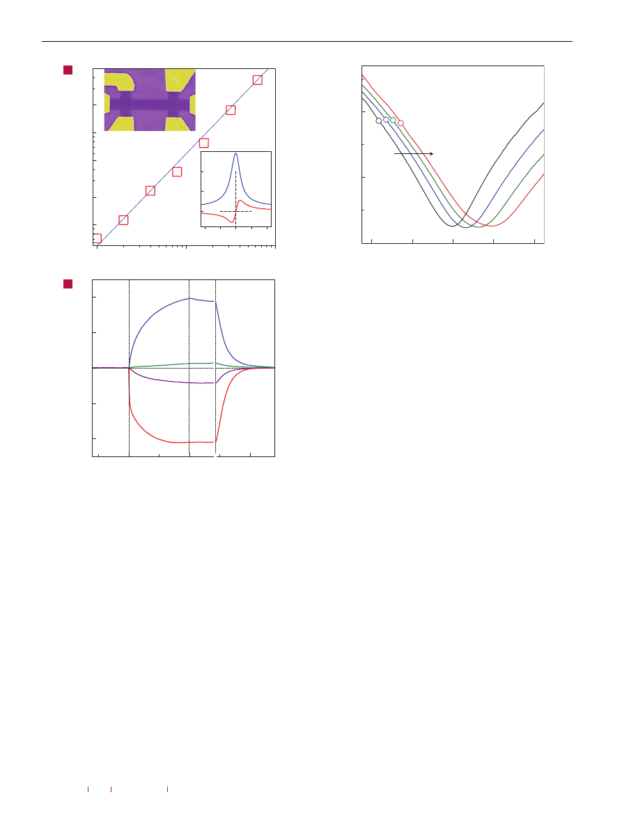
Figure 1
Sensitivity of graphene to chemical doping. a, Concentration,
1n, of
chemically induced charge carriers in single-layer graphene exposed to different
concentrations, C, of NO
2
. Upper inset: Scanning electron micrograph of this device
(in false colours matching those seen in visible optics). The scale of the micrograph
is given by the width of the Hall bar, which is 1 µm. Lower inset: Characterization of
the graphene device by using the electric-field effect. By applying positive (negative)
V
g
between the Si wafer and graphene, we induced electrons (holes) in graphene in
concentrations n =
αV
g
. The coefficient
α ≈ 7.2×10
10
cm
−
2
V
−
1
was found from
Hall-effect measurements
. To measure Hall resistivity,
ρ
xy
, B = 1 T was applied
perpendicular to graphene’s surface. b, Changes in resistivity,
ρ, at zero B caused
by graphene’s exposure to various gases diluted in concentration to 1 p.p.m. The
positive (negative) sign of changes is chosen here to indicate electron (hole) doping.
Region I: the device is in vacuum before its exposure; II: exposure to a 5 l volume of
a diluted chemical; III: evacuation of the experimental set-up; and IV: annealing at
150
◦
C. The response time was limited by our gas-handling system and a
several-second delay in our lock-in-based measurements. Note that the annealing
caused an initial spike-like response in
ρ, which lasted for a few minutes and was
generally irreproducible. For clarity, this transient region between III and IV
is omitted.
of adsorbed gas molecules between different surfaces in the insert.
After a near-equilibrium state was reached, we evacuated the
container again, which led only to small and slow changes in
ρ
(region III in Fig. 1b), indicating that adsorbed molecules were
–40
–20
0
20
40
0
1
2
V
g
(V)
σ
(k
Ω
–1
)
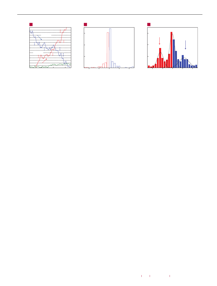
Figure 2
Constant mobility of charge carriers in graphene with increasing
chemical doping. Doping increased from zero (black curve) to ∼1
.5×10
12
cm
−
2
(red curve) due to increasing exposure to NO
2
. Conductivity,
σ, of single-layer
graphene away from the neutrality point changes approximately linearly with
increasing V
g
and the steepness of the
σ(V
g
) curves (away from the neutrality point)
characterizes the mobility,
µ (refs 6–9). Doping with NO
2
adds holes but also
induces charged impurities. The latter apparently do not affect the mobility of either
electrons or holes. The parallel shift implies a negligible scattering effect of the
charged impurities induced by chemical doping. The open symbols on the curves
indicate the same total concentration of holes, n
t
(∼2
.7×10
12
cm
−
2
), as found
from Hall measurements. The practically constant
σ for the same n
t
yields
that the absolute mobility,
µ = σ/n
t
e, as well as the Hall mobility are
unaffected by chemical doping. For further analysis and discussions, see the
Supplementary Information.
strongly attached to the graphene devices at room temperature.
Nevertheless, we found that the initial undoped state could be
recovered by annealing at 150
◦
C in vacuum (region IV). Repetitive
exposure–annealing cycles showed no ‘poisoning’ effects of these
chemicals (that is, the devices could be annealed back to their initial
state). A short-time ultraviolet illumination offered an alternative
to thermal annealing.
To gain further information about the observed chemical
response, we simultaneously measured changes in
ρ
xx
and
ρ
xy
caused by gas exposure, which allowed us to find directly (1)
concentrations,
1n
, of chemically induced charge carriers, (2)
their sign and (3) mobilities. The Hall measurements revealed that
NO
2
, H
2
O and iodine acted as acceptors, whereas NH
3
, CO and
ethanol were donors. We also found that, under the same exposure
conditions,
1n
depended linearly on the concentration,
C
, of an
examined chemical (see Fig. 1a). To achieve the linear conductance
response, we electrically biased our devices (by more than
±
10 V)
to higher-concentration regions, away from the neutrality point, so
that both
σ = neµ
and Hall conductivity,
σ
xy
=
1
/ρ
xy
=
ne
/B
, were
proportional to
n
. The linear response
as a function of
C
should greatly simplify the use of graphene-based
sensors in practical terms.
Chemical doping also induced impurities in graphene in
concentrations
N
i
=
1n
. However, despite these extra scatterers,
we found no notable changes in
µ
even for
N
i
exceeding
10
12
cm
−
2
. Figure 2 shows this unexpected observation by showing
the electric-field effect in a device repeatedly doped with
NO
2
. V-shaped
σ(V
g
)
curves characteristic for graphene
nature
materials
VOL 6 SEPTEMBER 2007 www.nature.com/naturematerials
653
©
2007
Nature Publishing Group
LETTERS
0
10
1e
1e
20
30
Changes in
xy
(Ω
)
t (s)
ρ
0
–4
–2
0
2
4
δ
–4
–2
0
2
4
200
400
600
0
200
400
600
R (
Ω)
δR (
Ω)
Number of steps
Number of steps
Adsorption
Desorption
Desorption events
Adsorption events
+1e
–1e
0
200
400
600
a
b
c
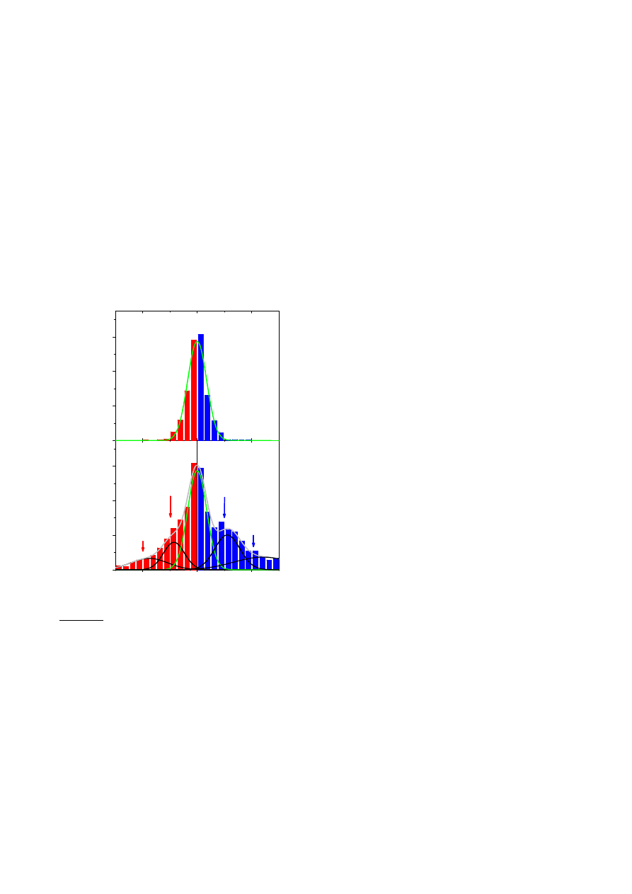
Figure 3
Single-molecule detection. a, Examples of changes in Hall resistivity observed near the neutrality point (|n|
< 10
11
cm
−
2
) during adsorption of strongly diluted NO
2
(blue curve) and its desorption in vacuum at 50
◦
C (red curve). The green curve is a reference—the same device thoroughly annealed and then exposed to pure He. The
curves are for a three-layer device in B = 10 T. The grid lines correspond to changes in
ρ
xy
caused by adding one electron charge, e (δR ≈ 2
.5 ), as calibrated in
independent measurements by varying V
g
. For the blue curve, the device was exposed to 1 p.p.m. of NO
2
leaking at a rate of ≈10
−
3
mbar l s
−
1
. b,c, Statistical distribution of
step heights, δR, in this device without its exposure to NO
2
(in helium) (b) and during a slow desorption of NO
2
(c). For this analysis, all changes in
ρ
xy
larger than 0
.5 and
quicker than 10 s (lock-in time constant was 1 s making the response time of ≈6 s) were recorded as individual steps. The dotted curves in textbfc are automated gaussian
fits (see the Supplementary Information).
can be seen. Their slopes away from the neutrality point provide
a measure of impurity scattering (so-called field-effect mobility,
µ = 1σ/1ne = 1σ/eα1V
g
). The chemical doping only shifted
the curves as a whole, without any significant changes in their
shape, except for the fact that the curves became broader around the
neutrality point (the latter effect is discussed in the Supplementary
Information). The parallel shift unambiguously proves that the
chemical doping did not affect scattering rates. Complementary
measurements in magnetic field showed that the Hall-effect
mobility,
µ = ρ
xy
/ρ
xx
B
, was also unaffected by the doping
and exhibited values very close to those determined from the
electric-field effect. Further analysis yields that chemically induced
ionized impurities in graphene in concentrations
>
10
12
cm
−
2
(that
is, less than 10 nm apart) should not be a limiting factor for
µ
until
it reaches values of the order of 10
5
cm
2
V
−
1
s
−
1
, which translates
into a mean free path as large as
≈
1
µ
m (see the Supplementary
Information). This is in striking contrast with conventional
two-dimensional systems, in which such high densities of charged
impurities are detrimental for ballistic transport, and also disagrees
by a factor of
>
10 with recent theoretical estimates for the
case of graphene
. Our observations clearly raise doubts about
charged impurities being the scatterers that currently limit
µ
in
graphene
. In the Supplementary Information, we show that a
few-nanometre-thick layer of absorbed water provides sufficient
dielectric screening to explain the suppressed scattering on charged
impurities. We also suggest there that microscopic corrugations of
a graphene sheet
could be dominant scatterers.
The detection limit for solid-state gas sensors is usually defined
as the minimal concentration that causes a signal exceeding
the sensors’ intrinsic noise
. In this respect, a typical noise
level in our devices,
1ρ/ρ ≈
10
−
4
(see Fig. 1b), translates into
the detection limit of the order of 1 p.p.b. This already puts
graphene on par with other materials used for most sensitive gas
sensors
. Furthermore, to demonstrate the fundamental limit
for the sensitivity of graphene-based gas sensors, we optimized
our devices and measurements as described in the Supplementary
Information. In brief, we used high driving currents to suppress the
Johnson noise, annealed devices close to the neutrality point, where
relative changes in
n
were largest for the same amount of chemical
doping, and used few-layer graphene (typically, 3–5 layers), which
allowed a contact resistance of
≈
100
, much lower than for single-
layer graphene. We also used the Hall geometry that provided the
largest response to small changes in
n
near the neutrality point
(see Fig. 1a, lower inset). In addition, this measurement geometry
minimizes the sensitive area to the central region of the Hall cross
(
≈
1
µ
m
2
in size) and allows changes in
ρ
xy
to be calibrated directly
in terms of charge transfer by comparing the chemically induced
signal with the known response to
V
g
. The latter is important for
the low-concentration region, where the response of
ρ
xy
to changes
in
n
is steepest, but there is no simple relation between
ρ
xy
and
n
.
Figure 3 shows changes in
ρ
xy
caused by adsorption and
desorption of individual gas molecules. In these experiments, we
first annealed our devices close to the pristine state and then
exposed them to a small leak of strongly diluted NO
2
, which was
adjusted so that
ρ
xy
remained nearly constant over several minutes
(that is, we tuned the system close to thermal equilibrium where
the number of adsorption and desorption events within the Hall
cross area was reasonably small). In this regime, the chemically
induced changes in
ρ
xy
were no longer smooth but occurred in
a step-like manner as shown in Fig. 3a (blue curve). If we closed
the leak and started to evacuate the sample space, similar steps
occurred but predominantly in the opposite direction (red curve).
For finer control of the adsorption/desorption rates, we found it
useful to slightly adjust the temperature while keeping the same
leak rate. The characteristic size,
δ
R
, of the observed steps in
terms of ohms depended on
B
, the number of graphene layers
and, also, varied strongly from one device to another, reflecting the
fact that the steepness of the
ρ
xy
curves near the neutrality point
(see Fig. 1a, lower inset) could be different for different devices
.
However, when the steps were recalibrated in terms of equivalent
changes in
V
g
, we found that to achieve the typical value of
δ
R
it always required exactly the same voltage changes,
≈
1
.
5 mV, for
all of our 1
µ
m devices and independently of
B
. The latter value
corresponds to
1n ≈
10
8
cm
−
2
and translates into one electron
charge,
e
, removed from or added to the area of 1
×
1
µ
m
2
of
the Hall cross (note that changes in
ρ
xy
as a function of
V
g
were
smooth, that is, no charge quantization in the devices’ transport
characteristics occurred—as expected). As a reference, we repeated
654
nature
materials
VOL 6 SEPTEMBER 2007 www.nature.com/naturematerials
©
2007
Nature Publishing Group

LETTERS
the same measurements for devices annealed for 2 days at 150
◦
C
and found no or very few steps (green curve).
The curves shown in Fig. 3a clearly suggest individual
adsorption and desorption events but statistical analysis is required
to prove this. To this end, we recorded a large number of curves
such as that in Fig. 3a (
≈
100 h of continuous recording). The
resulting histograms with and without exposure to NO
2
are shown
in Fig. 3b,c (a histogram for another device is shown in the
Supplementary Information). The reference curves exhibited many
small (positive and negative) steps, which gave rise to a ‘noise
peak’ at small
δ
R
. Large steps were rare. On the contrary, slow
adsorption of NO
2
or its subsequent desorption led to many
large, single-electron steps. The steps were not equal in size,
as expected, because gas molecules could be adsorbed anywhere
including the fringes of the sensitive area, which should result in
varying contributions. Moreover, because of a finite time constant
(1 s) used in these sensitive measurements, random resistance
fluctuations could overlap with individual steps either enhancing
or reducing them and, also, different events could overlap in time
occasionally (such as the largest step on the red curve in Fig. 3a,
which has a quadruple height). The corresponding histogram
(Fig. 3c) shows the same ‘noise peak’ as the reference in Fig. 3b
but, in addition, there are two extra maxima that are centred
at a value of
δ
R
, which corresponds to removing/adding one
acceptor from the detection area. The asymmetry in the statistical
distribution in Fig. 3c corresponds to the fact that single-acceptor
steps occur predominantly in one direction, that is, NO
2
on-average
desorbs from graphene’s surface in this particular experiment. The
observed behaviour leaves no doubt that the changes in graphene
conductivity during chemical exposure were quantized, with each
event signalling adsorption or desorption of a single NO
2
molecule.
In summary, graphene-based gas sensors allow the ultimate
sensitivity such that the adsorption of individual gas molecules
could be detected. Large arrays of such sensors would increase
the catchment area
, allowing higher sensitivity for short-time
exposures and the detection of active (toxic) gases in as minute
concentrations as practically desirable. The epitaxial growth of few-
layer graphene
offers a realistic promise of mass production
of such devices. Our experiments also show that graphene is
sufficiently electronically quiet to be used in single-electron
detectors operational at room temperature
and in ultrasensitive
sensors of magnetic field or mechanical strain
, in which the
resolution is often limited by 1
/f
noise. Equally important
is the
demonstrated possibility of chemical doping of graphene by both
electrons and holes in high concentrations without deterioration of
its mobility. This should allow microfabrication of p–n junctions,
which attract significant interest from the point of view of both
fundamental physics and applications. Despite its short history,
graphene is considered to be a promising material for electronics by
both academic and industrial researchers
, and the possibility
of its chemical doping further improves the prospects of graphene-
based electronics.
Received 14 May 2007; accepted 2 July 2007; published 29 July 2007.
References
1. Moseley, P. T. Solid state gas sensors.
Meas. Sci. Technol.
8, 223–237 (1997).
2. Capone, S.
et al
. Solid state gas sensors: State of the art and future activities.
J. Optoelect. Adv. Mater.
5, 1335–1348 (2003).
3. Kong, J.
et al
. Nanotube molecular wires as chemical sensors.
Science
287, 622–625 (2000).
4. Collins, P. G., Bradley, K., Ishigami, M. & Zettl, A. Extreme oxygen sensitivity of electronic properties
of carbon nanotubes.
Science
287, 1801–1804 (2000).
5. Dutta, P. & Horn, P. M. Low-frequency fluctuations in solids: 1/f noise.
Rev. Mod. Phys.
53,
497–516 (1981).
6. Geim, A. K. & Novoselov, K. S. The rise of graphene.
Nature Mater.
6, 183–191 (2007).
7. Novoselov, K. S.
et al
. Two dimensional atomic crystals.
Proc. Natl Acad. Sci. USA
102,
10451–10453 (2005).
8. Novoselov, K. S.
et al
. Two dimensional gas of massless Dirac fermions in graphene.
Nature
438,
197–200 (2005).
9. Zhang, Y., Tan, J. W., Stormer, H. L. & Kim, P. Experimental observation of the quantum Hall effect
and Berry’s phase in graphene.
Nature
438, 201–204 (2005).
10. Dresselhaus, M. S. & Dresselhaus, G. Intercalation compounds of graphite.
Adv. Phys.
51,
1–186 (2002).
11. Ando, T. Screening effect and impurity scattering in monolayer graphene.
J. Phys. Soc. Jpn.
75,
074716 (2006).
12. Nomura, K. & MacDonald, A. H. Quantum Hall ferromagnetism in graphene.
Phys. Rev. Lett.
96,
256602 (2006).
13. Hwang, E. H., Adam, S. & Das Sarma, S. Carrier transport in two-dimensional graphene layers.
Phys.
Rev. Lett.
98, 186806 (2007).
14. Morozov, S. V.
et al
. Strong suppression of weak localization in graphene.
Phys. Rev. Lett.
97,
016801 (2006).
15. Meyer, J. C.
et al
. The structure of suspended graphene sheets.
Nature
446, 60–63 (2007).
16. Sheehan, P. E. & Whitman, L. J. Detection limits for nanoscale biosensors.
Nano Lett.
5,
803–807 (2005).
17. Berger, C.
et al
. Electronic confinement and coherence in patterned epitaxial graphene.
Science
312,
1191–1196 (2006).
18. Ohta, T., Bostwick, A., Seyller, T., Horn, K. & Rotenberg, E. Controlling the electronic structure of
bilayer graphene.
Science
313, 951–954 (2006).
19. Barbolina, I. I.
et al
. Submicron sensors of local electric field with single-electron resolution at room
temperature.
Appl. Phys. Lett.
88, 013901 (2006).
20. Bunch, J. S.
et al
. Electromechanical resonators from graphene sheets.
Science
315, 490–493 (2007).
21. Zhou, C., Kong, J., Yenilmez, E. & Dai, H. Modulated chemical doping of individual carbon
nanotubes.
Science
290, 1552–1555 (2000).
22. Obradovic, B.
et al
. Analysis of graphene nanoribbons as a channel material for field-effect
transistors.
Appl. Phys. Lett.
88, 142102 (2006).
Acknowledgements
We thank A. MacDonald, S. Das Sarma and V. Falko for illuminating discussions. This work was
supported by the EPSRC (UK) and the Royal Society. M.I.K. acknowledges financial support from
FOM (Netherlands).
Correspondence and requests for materials should be addressed to K.S.N.
Supplementary Information accompanies this paper on www.nature.com/naturematerials.
Author contributions
K.S.N. designed the experiment and carried out both experimental work and data analysis, A.K.G.
suggested the research direction and wrote the manuscript, F.S. and P.B. made graphene devices,
S.V.M. and E.W.H. helped with experiments and their analysis and M.I.K. provided theory support. All
authors participated in discussions of the research.
Competing financial interests
The authors declare no competing financial interests.
Reprints and permission information is available online at http://npg.nature.com/reprintsandpermissions/
nature
materials
VOL 6 SEPTEMBER 2007 www.nature.com/naturematerials
655
©
2007
Nature Publishing Group
©
2007
Nature Publishing Group
1
-0 .1
0 .0
0 .1
0
1 0 0 0
2 0 0 0
3 0 0 0
0
1 0 0 0
2 0 0 0
3 0 0 0
a
+ 1 e
+ 2 e
-2 e
δ
R (
Ω )
-1 e
b
num
be
r of s
te
ps
Figure S1. Statistical distribution of step heights
δ
R in a (5-
7)-layer device during its exposure to pure helium (a) and a
small leak (10
-3
mbar
⋅l/s) of NO
2
diluted in a concentration
of 1 ppm (b). An example of the raw data is shown by the
blue curve in Fig. 3a. Red and blue bars indicate steps in the
opposite directions (desorption and adsorption events,
respectively). The histogram in (a) was first fitted by a
Gaussian curve (green). Then, assuming that the noise peak
does not change, the remaining statistical distribution was
fitted by 4 Gaussian curves (black) allowing all four
amplitudes and positions to be chosen automatically by the
Origin-7.0 fitting routine. The resulting total of 5 Gaussians
accurately fits the whole distribution (grey curve). Three
Gaussians also give a reasonable (but less perfect) fit with
extra peaks centred at ±0.05Ohm.
SUPPLEMENTARY INFORMATION
Experimental Procedures
We employed low-frequency (30 to 300 Hz) lock-in measurements and used relatively high driving currents of
≈30 µA/µm. The latter suppressed any voltage noise, so that the remaining fluctuations in the measured
resistance were intrinsic, that is, due to thermal switching of unstable defects [5]. Switching defects are known to
lead to telegraph noise or, if many such defects are present, to 1/f-noise, which fundamentally limits the
sensitivity of all thin-film sensors at room temperature [5]. In this respect, graphene devices were found to
exhibit an exceptionally low level of intrinsic noise, as compared to any other detector based on charge
sensitivity (see [19] and references therein). The lowest level of noise was found in devices with the highest
mobility (>10,000 cm
2
/Vs) and the lowest contact resistance. Sensors made from few-layer graphene (3 to 5
layers) were most electrically quiet, probably because their contact resistance could be as low as
≈50 Ohm, as
compared with typically
≈1kOhm for our single-layer devices.
To maximize the sensitivity, we tested various regimes and various device’s sizes. The maximum signal-to-noise
ratio was found for the Hall geometry and measurements at low doping (<10
11
cm
-2
or |V
g
|<1V). In this regime,
the noise in terms of Ohms was not at its lowest but
this was compensated by the steepest response in
ρ
xy
to an induced electric charge (see the lower inset in
Fig. 1a). The optimum size was found to be
≈1µm.
Smaller devices exhibited higher 1/f-noise
(presumably due to defects at sample edges), whereas
larger sizes lead to smaller relative changes in
ρ
xy
in
response to the same number of electrons. As an
indicator of sufficiently low noise we used the
possibility to detect changes with varying gate
voltage by less than 1mV. This corresponds to
changes of less than one elementary charge e inside
the sensitive area of the Hall cross of 1x1
µm
2
in size.
Statistical Distribution of Single-Molecule Steps
To complement the histograms in Fig. 3 and
demonstrate their generality, Fig. S1 shows another
example of a histogram for step-like changes in
ρ
xy
.
These data were obtained for a different device, in a
different magnetic field (B=4T) and during
graphene’s exposure to NO
2
, that is, for the regime of
average adsorption, rather than desorption shown in
Fig. 3. The 50 times smaller value of the single-
electron steps (
≈0.05 Ohm) in this case is due to
thicker graphene (5-7 layers), smaller B and a wider
transition region near the neutrality point, which
leads to less steep changes in
ρ
xy
as a function of n.
This value of
≈0.05 Ohm was again calibrated using
changes in V
g
by
≈1.4mV, which adds 1e to the Hall
cross area of 1
µm
2
. Due to the weaker response, there
is a broad “noise” peak that dominates the statistical
distributions in both cases, with and without NO
2
exposure. However, it is clear that when the device
was exposed to NO
2
, the statistical distribution
became much wider, asymmetric with side wings and
cannot be fitted by a single Gaussian. The changes
caused by NO
2
exposure can only be fitted by adding
©
2007
Nature Publishing Group
2
t (s)
1000
1000
0
ρ
xx
&
ρ
xy
(k
Ω
)
4
0
2
ρ
xx
ρ
xy
NO
2
NH
3
t (s)
1000
1000
0
ρ
xx
&
ρ
xy
(k
Ω
)
4
0
2
ρ
xx
ρ
xy
NO
2
NH
3
Figure S2. Accumulation of dopants on graphene.
Changes in the longitudinal (
ρ
xx
) and Hall (
ρ
xy
) resistivity
of graphene exposed to a continuous supply of strongly-
diluted NH
3
(right part). After the exposure, the device
was annealed close to the pristine state and then exposed
to NO
2
in exactly the same fashion (left part). Here,
measurements of both
ρ
xx
and
ρ
xy
were carried out in
field B=1T.
two additional Gaussian peaks for both negative and positive
δ
R. However, the automated fitting procedures
favour four additional peaks centred at
≈0.05 and 0.1 Ohm, which exactly corresponds to the transfer of e and
2e. The 2e-peak is consistent with events where individual adsorption/desorption steps were not time-resolved
and resulted in steps of the double height. The observed asymmetry in the histogram corresponds to the fact that
large steps occur predominantly in one direction, that is, the adsorption is stronger than desorption, and
graphene’s doping gradually increases with time (compare with the asymmetry in Fig. 3c).
Accumulation of chemical doping
We found that our graphene devices did not exhibit the saturation in the detected signal during long exposures to
small (ppm) concentrations C of active gases. This means that the effect of chemical doping in graphene is
cumulative. In the particular experiment shown in Fig. 1b, the apparent saturation observed in region II was
found to be caused by a limited amount of gas molecules able to reach the micron-sized sensitive area, because
of the competition with other, much larger adsorbing areas in the experimental setup. This is in good agreement
with the theory of chemical detectors of a finite size [16]. Figure S2 illustrates the accumulation effect by
showing changes in
ρ
xx
and
ρ
xy
as a function of exposure time t for the same sensor as in Fig. 1b but exposed to a
constant flow of NO
2
and NH
3
(in ppm concentrations) rather than to a limited volume of these chemicals as it
was the case of Fig. 1b of the main text. In Fig. S2, graphene’s doping continues to increase with time t because
of the continuous supply of active molecules into the sensitive area (in contrast to the experiment shown in Fig.
1). Within an hour, the device’s resistivity changed by 300%. Longer exposures and high C allowed us to reach a
doping level up to
≈2x10
13
cm
-2
. Note that the behaviour in Fig. S2 clearly resembles the corresponding
dependences in the lower inset of Fig. 1a but charge carriers in Fig. S2 are induced by chemical rather than
electric-field doping. The observed accumulation effect yields that the detection limits for graphene sensors can
be exceedingly small during long exposures that allow a sufficient amount of gas molecules to be adsorbed
within the sensitive area. Alternatively, large arrays of
such sensors would increase the catchment area and
should allow a much higher sensitivity also for short-
time exposures [16].
The mechanism of chemical doping in graphene is
expected to be similar to the one in carbon nanotubes.
Unfortunately, the latter remains unexplained and still
controversial, being attributed to either charge transfer
or changes in scattering rates or changes in contact
resistance [3,S1,S2,S3,S4]. Our geometry of four-probe
measurements rules out any effect due to electrical
contacts, whereas the mobility measurements prove that
the charge transfer is the dominant mechanism of
chemical sensing. Also, it is believed that the presence
of a substrate can be important for chemical sensing in
carbon nanotubes. We cannot exclude such influence,
although this is rather unlikely for flat graphene, where
doping mostly occurs from the top. We also note that
hydrocarbon residues on graphene’s surface (including
remains of electron-beam resist) are practically
unavoidable, and we believe that such polymers may
effectively “functionalize” graphene, acting as both
adsorption sites and intermediaries in charge transfer
(see further).
Constant mobility of charge carriers with increasing chemical doping
No noticeable changes in
µ
with increasing chemical doping were observed in our experiments, as discussed in
the main text. In order to estimate quantitatively the extent, to which chemical doping may influence carrier
©
2007
Nature Publishing Group
3
mobility in graphene, we used the following analysis (see Fig. S3). For
each level of chemical doping, we measured the dependence of
σ
on V
g
(such as in Fig. 2) and the Hall effect in B =1T. The latter allowed us to
find gate voltages that correspond exactly the same total concentration
n
t
=B/e
ρ
xy
which combines the concentrations induced by chemical (N
i
)
and electric-field (n=
αV
g
) doping. For example, the symbols in Fig. 2
indicate n
t
≈2.7x10
12
cm
-2
. The fact that, for the same n
t
,
σ
remains
unchanged, independently of chemical doping, (Fig. 2) yields that the
Hall mobility
µ
=
ρ
xy
/
ρ
xx
B =
σ
/en
t
does not change. Furthermore, we
also calculated the field-effect mobility defined as
µ
=
∆
σ
/
∆n. To this
end, the curves were first fitted by linear dependences over an interval
of ±10V. From the found slopes
∆
σ
/
∆V
g
, we extracted the field-effect
mobility
µ
=
∆
σ
/e
α∆V
g
. An example of the latter for the same n
t
≈2.7x10
12
cm
-2
is plotted as a function of N
i
in Fig. S3.
Figs 2 and S3 show that both Hall and field-effect
µ
were practically independent of chemical doping. Only for
N
i
>>10
12
cm
-2
, we usually found notable changes in the shape of
σ
(V
g
)-curves, which often became rather
deformed. The latter effect remains to be understood, which unfortunately does not allow us to draw quantitative
conclusions about the exact behaviour of
µ
at very high chemical doping. However, even for
∆n ≈10
13
cm
-2
, we
observed the electric-field mobility exceeding 2,000 cm
2
/Vs, which puts only the lower limit on
µ
at such high
doping. Also, note a significant broadening of the transition region near NP caused by chemical doping, which is
clearly seen on
σ
(V
g
)-curves in Fig. 2. This broadening could in principle be attributed to an increasingly
inhomogeneous distribution of dopants [6,13]. However, such a strong broadening was found to be specific for
NO
2
and can be explained by two types of acceptor levels (monomers and dimers of NO
2
) [S5]. This broadening
is irrelevant for our main conclusion that graphene’s mobility is unaffected by chemical doping, because
µ
is
defined at high n, away from NP [6-9].
Fig. S3 yields that charged impurities in concentration N
i
≈10
12
cm
-2
do not change mobility
µ
≈5,000 cm
2
/Vs
within an experimental accuracy of
≈5%. This implies that, if all other sources of scattering are eliminated, such
a level of chemical doping should still allow
µ
as high as 10
5
cm
2
/Vs. This value is in strong disagreement (by a
factor of 20) with the current theoretical estimates for scattering rates in graphene [11-13], which predict a
concentration-independent mobility of
≈5,000 cm
2
/Vs for charged impurities in concentration 10
12
cm
-2
. Note
that these theories take into account the Dirac-like spectrum of graphene, which already results in a strongly
reduced scattering in comparison with conventional, Schrödinger-like 2D systems (see below).
There are three possible ways to reconcile the experiment and theory. First, chemical doping can neutralize
ionized impurities of the opposite sign, if a mixture of donors and acceptors in a concentration of
≈10
12
cm
-2
is
already present at the surface of graphene or in a substrate [S6]. In this case, mobility
µ
may even temporarily
increase with increasing chemical doping [S6]. However, a large experimental range of N
i
over which
µ
remains
practically unaffected for both electron and hole conductivities (and remains relatively high at N
i
>10
13
cm
-2
)
seems to rule out this mechanism as dominant in our case. Second, absorption sites can be at sample edges or at
some distance above a graphene sheet. The former is unlikely for the lack of a sufficient number of broken bonds
to accommodate all the dopants along the edges. However, we cannot rule out that a hydrocarbon residue can
somehow act as a transfer medium, providing an increased distance between adsorbed impurities and graphene.
Indeed, even though our devices were thoroughly cleaned after microfabrication procedures, a thin polymer layer
(of about 1nm thick) was observed in AFM and some TEM measurements. This separation is however
insufficient [12,13] to explain the observed reduction in scattering rates by a factor of >20. The third possibility
is due to absorbed water above or below a graphene sheet, which has a huge dielectric constant
ε
w
=80 and can
provide additional screening [S7]. Indeed, when calculating scattering rates in graphene, it is normally assumed
that graphene is neighboured by vacuum and SiO
2
, a space with an effective dielectric constant
ε
eff
= (
ε
SiO2
+ 1)/2
≈2.5 [12,13]. We argue that the presence of a few-nm-thick layer of absorbed water can dramatically increase
ε
eff
and suppress the scattering contribution of charged impurities below the current detection limit.
N
im
(10
12
cm
-2
)
µ
(1
0
3
cm
2
/Vs)
0
2
4
6
0
1
2
N
im
(10
12
cm
-2
)
µ
(1
0
3
cm
2
/Vs)
0
2
4
6
0
1
2
0
2
4
6
0
2
4
6
0
1
2
0
1
2
Figure S3. Changes in carrier mobility
with increasing the concentration of
acceptors induced by NO
2
doping

©
2007
Nature Publishing Group
4
It is well known that, unless heated at several hundred C
° in high vacuum, all surfaces are covered with absorbed
water. For example, SiO
2
is normally covered by 2 to 3 nm of water, even in vacuum [S8]. Our analysis of the
corresponding electrostatic problem shows that the effective dielectric constant for a graphene sheet that is
neighboured by an additional layer of absorbed water with thickness D can be described by
ε
eff
(k)
≈ [
ε
SiO2
+ 1
+
ε
w
tanh(k
F
D)]/2 where k
F
is the Fermi wave vector. For a typical concentration of 10
12
cm
-2
,
ε
eff
≈10 and 22 for
D = 1 and 3nm, respectively. As the scattering rate by charged impurities depends quadratically on
ε
eff
, this
additional dielectric screening is sufficient to explain the observed constant mobility with increasing chemical
doping. The use of water as a dielectric media suppressing scattering in graphene is an interesting effect that can
be used in future to improve the electronic quality of graphene devices.
On alternative mechanism limiting carrier mobility in graphene
Our experiments and discussion above show that charged impurities are unlikely to be dominant scatterers in the
existing graphene samples. Below we suggest an alternative temperature-independent scattering mechanism but
let us first review other possibilities.
It has been shown that scattering on a short-range potential with a radius R
≈a results in low excess resistivity
ρ
≈(h/4e
2
)N
i
R
2
where a is the interatomic distance [11-13,S9]. This scattering mechanism can be neglected for any
feasible concentration of short-range impurities. Note that, in a normal 2D electron system with a parabolic
spectrum, the same concentration of short-range impurities leads to a much higher resistivity
ρ
≈(h/4e
2
)(N
i
/n)ln
2
(R/
λ
) [S10].
One can understand so little scattering on a short-range potential in graphene by
using an analogy with the diffraction of light on small obstacles, which becomes inefficient for wavelengths
λ
>>R. This analogy with light is inapplicable for 2D Schrödinger-like electrons because in the latter case a short-
range potential always leads to a resonant-like scattering [S9,S10]. On the contrary, for 2D Dirac fermions, the
scattering becomes efficient only if an impurity has a bound level at the same energy as that of incident fermions
[S9], which would be unusual for graphene because of the Klein tunnelling [6].
To explain the observed values of
µ
in graphene and, particularly, its practically constant value with increasing
V
g
[6-9], a scattering on a long-range Coulomb potential due to charged impurities was invoked [11-13].
Coulomb impurities in a 2D gas of Dirac fermions result in its resistivity
ρ
≈α(h/4e
2
)(N
i
/n) where the coefficient
α is predicted to be ≈0.2 [13], which yields
µ
≈5,000 cm
2
/Vs for N
i
≈10
12
cm
-2
. As discussed in the previous
section, our experiments prove that chemical doping at N
i
≈10
12
cm
-2
should allow
µ
≈10
5
cm
2
/Vs, which casts
serious doubts that ionized impurities are currently a limiting factor for
µ
in graphene.
Therefore, it is sensible to consider alternative scattering mechanisms. To this end, it was experimentally found
that graphene is not flat but exhibits random nm-size ripples that involve a large elastic strain of
≈1% [14,15].
The influence of such ripples on
ρ
has not been discussed so far but it was shown that the associated elastic
strain effectively results in random vector [6,14] and electric [S11] potentials. The induced vector potential is
equivalent to a random sign-changing B exceeding 1 Tesla, which was shown to be sufficient for suppressing
weak localization corrections in graphene [6,14]. Below, we show that this random B can induce significant
scattering (also, see [S12]).
Resistivity of a rippled graphene sheet
Applying the standard procedures for calculating the mean-free time τ [11-13,S8-S10] but now for the case of a
scattering potential with a spinor structure
σ
r
r
V
, one can write
( )
)
1
(
2
1
S
V
V
E
N
F
k
q
q
q
F
≈
−
≈
r
r
r
r
h
π
τ
where
( )
F
E
N
is the density of states at the Fermi energy and q the wave vector. For a curved surface with the
fluctuating height
( )
y
x
h ,
counted from the average plane
0
=
z
, the vector potential is proportional to in-plane
deformations and, thus, quadratic in the derivatives
y
h
x
h
∂
∂
∂
∂
,
(explicit expressions can be found in [S9]; see
equations (2)-(5)). This leads to the following expression
(
)
[
]
(
)
[
]
)
2
(
2
2
1
1
2
2
1
2
2
1
1
S
q
q
q
q
q
q
h
h
h
h
a
v
V
V
q
q
q
q
q
q
q
q
F
q
q
r
r
r
r
r
r
h
r
r
r
r
r
r
r
r
r
r
r
r
⋅
−
⋅
−
⎟
⎠
⎞
⎜
⎝
⎛
≈
∑
−
+
−
−
−
©
2007
Nature Publishing Group
5
where
F
v
is the Fermi velocity, a the lattice constant and
q
h
the Fourier coefficients.
To proceed further, one needs specify the nature of ripples, because the correlation function in the right-hand
side of (S2) depends on a distribution of elastic strain. To this end, we first assume that the ripples observed in
graphene initially appear as a result of thermal fluctuations [S13] Then, using the standard harmonic
approximation, it is straightforward to estimate (S2). Indeed, the average potential energy per bending mode
2
/
2
4
q
q
h
q
E
κ
=
r
should be equal to
2
/
T
k
B
(κ
≈1eV is the bending stiffness of graphene [S11]), which yields
)
3
(
4
2
S
q
T
k
h
B
q
κ
=
r
Note that thermal fluctuations with small q are extremely soft, which can lead to a crumpling instability, that is,
the amplitude of fluctuations normal to the membrane plane would grow linearly with increasing the membrane
size [S13]. However, an anharmonic coupling between bending and stretching modes partially suppresses the
growth of such fluctuations at small q [S13]
)
4
(
1
0
4
2
S
q
q
q
h
q
η
⎟⎟
⎠
⎞
⎜⎜
⎝
⎛
≈
r
where
a
b
q
/
1
/
0
≈
≈
κ
is a typical cut-off vector on interatomic distances, b the 2D bulk modulus,
8
.
0
≈
η
the bending stiffness exponent [S13]. Changes in the asymptotic behaviour happen for a typical wave vector
(
)
η
κ
/
1
0
*
/
T
k
q
q
B
=
, at which expressions (S3) and (S4) become comparable. At room temperature, this yields
a
q
/
10
2
*
−
≈
.
Our crucial assumption is that the thermodynamic distribution of ripples becomes static (“quenched”) when a
graphene sheet is deposited on a substrate at some quench temperature T
q
(300K in our case). Indeed, it is
reasonable to suggest that during the deposition process graphene sticks to the substrate and cannot adopt a
ripple-free configuration or follow exactly the form prescribed by substrate’s own roughness [S14].
For carrier concentrations such that
*
q
k
F
≥
(that is always the case of our measurements of
µ), we can use (S3)
for the pair correlation function and the Wick theorem for the four-h correlation function in (S2), which allows
us to find the ripple resistivity as
(
)
)
5
(
/
4
2
2
S
n
a
T
k
e
h
q
B
Λ
≈
κ
ρ
where the factor Λ is of order of unity for
*
q
k
F
≅
and weakly depends on carrier concentration (as
(
)
*
2
/
ln
q
k
F
for
*
q
k
F
>>
). The above equation shows that thermodynamically-induced ripples lead to
µ practically
independent on n, as observed experimentally. Importantly, (S5) also yields
µ of the same order of magnitude as
found in graphene (one can interpret
(
)
2
/ a
T
k
q
B
κ
≈10
12
cm
-2
as an effective concentration of ripples).
Finally, we note that if ripples have an origin different from the one discussed above (for example, due to
intrinsic roughness of the SiO
2
substrate [S14]), then in order to calculate their scattering rates, one would have
to know an exact distribution of the associated strain [S15]. Furthermore, it is possible that a structural
distribution of ripples is dominated by ripples with a short-range scattering potential [S14] but resistivity is still
dominated by a minority of thermodynamically-induced ripples with the long-range potential that is the only
efficient source of scattering in graphene.

©
2007
Nature Publishing Group
6
Supplementary References
S1. H. Chang, J. D. Lee, S. M. Lee, Y. H. Lee. Adsorption of NH
3
and NO
2
molecules on carbon nanotubes,
Appl. Phys. Lett. 79, 3863-3865 (2001).
S2. K. Bradley, J. P. Gabriel, M. Briman, A. Star, and G. Grüner. Charge transfer from ammonia physisorbed on
nanotubes, Phys. Rev. Lett. 91, 218301 (2003).
S3. S. Heinze, J. Tersoff, R. Martel, V. Derycke, J. Appenzeller, Ph. Avouris. Carbon nanotubes as Schottky
barrier transistors, Phys. Rev. Lett. 89, 106801 (2002).
S4. J. Zhang, A. Boyd, A. Tselev, M. Paranjape, and P. Barbara. Mechanism of NO
2
detection in carbon
nanotube field effect transistor chemical sensors, Appl. Phys. Lett. 88, 123112 (2006).
S5. T.O. Wehling et al. Molecular Doping of Graphene. cond-mat/0703390.
S6. E.H. Hwang, S. Adam, and S. Das Sarma. Transport in chemically doped graphene in the presence of
adsorbed molecules. cond-mat/0610834.
S7. D. Jena, A. Konar. Enhancement of Carrier Mobility in Semiconductor Nanostructures by Dielectric
Engineering, Phys. Rev. Lett. 98, 136805 (2007).
S8. A. Opitz, M. Scherge, S.I.U. Ahmed, J.A. Schaefer. A comparative investigation of thickness measurements
of ultra-thin water films by scanning probe techniques, J. Appl. Phys. 101, 064310 (2007) and references therein.
S9. M.I. Katsnelson, K.S. Novoselov. Graphene: new bridge between condensed matter physics and quantum
electrodynamics. cond-mat/0703374.
S10. T. Ando, A.B. Fowler, F. Stern. Electronic properties of two-dimensional systems. Rev. Mod. Phys. 54,
437-672 (1982)
S11. A.H. Castro Neto, E.A. Kim. Charge inhomogeneity and the structure of graphene sheets. cond-
mat/0702562.
S12. A.K. Geim, S.J. Bending, I.V. Grigorieva. Ballistic two-dimensional electrons in a random magnetic field.
Phys. Rev. B 49, 5749-5752 (1994).
S13. D.R. Nelson, T. Piran, and S. Weinberg. Statistical mechanics of membranes and Surfaces. World
Scientific, Singapore, 2004.
S14. M. Ishigami, J. H. Chen, W. G. Cullen, M. S. Fuhrer, E. D. Williams. Atomic Structure of Graphene on
SiO
2
. Nano Lett. 7, 1643- 1648 (2007).
S15. D.V. Khveshchenko. Long-range-correlated disorder in graphene. Phys Rev B 75, 241406(R) (2007).
Document Outline
- Detection of individual gas molecules adsorbed on graphene
- Figure 1 Sensitivity of graphene to chemical doping.
- Figure 2 Constant mobility of charge carriers in graphene with increasing chemical doping.
- Figure 3 Single-molecule detection.
- References
- Acknowledgements
- Author contributions
- Competing financial interests
Wyszukiwarka
Podobne podstrony:
Naturemat 2007GasSensor
Molecular evolution of FOXP2, Nature
Zrozumieć Naturę Rzeczywistości
Hume A Treatise of Human Nature
On nature Butterflies
Foucault & Chomsky ?bate on Human Nature
blue nature MINERAŁY PIĘKNA
blue nature
NatureSexy1
North Light Books 1995 Drawing Nature ISBN 0891345795 148s
nature of human language
Nature2(3)
15 Nature Nano 3 210 215 2008id Nieznany (2)
a complete handbook of nature cure 6GF4BUMTKBPGURS62LOQQC4PI22YXTDWGWFQ5AY
The Nature of Mind Longchenpa
Fraassen; The Representation of Nature in Physics A Reflection On Adolf Grünbaum's Early Writings
Nature3(3)
POROD W EKSTAZIE PRZEWIDZIANY PRZEZ NATURE HORMO
30 Nature Mater 6 652 655 2007 Nieznany (2)
więcej podobnych podstron