Date: November, 2007 / Issue 1.0
Service Manual
Model : U990/KU990
Service Manual
U990/KU990
Internal Use Only

- 3 -
1. INTRODUCTION.................................. 5
1.1 Purpose ...................................................... 5
1.2 Regulatory Information ............................... 5
2. PERFORMANCE ..................................7
2.1 System Overview.........................................7
2.2 Usable environment.....................................8
2.3 Radio Performance......................................8
2.4 Current Consumption.................................16
2.5 RSSI BAR ..................................................17
2.6 Battery BAR ...............................................17
2.7 Sound Pressure Level ...............................18
2.8 Charging ....................................................18
3. TECHNICAL BRIEF............................19
3.1 General Description ...................................19
3.2 GSM Mode.................................................21
3.3 UMTS Mode...............................................25
3.4 LO generation and distribution circuits ......27
3.5 Off-chip RF Components ...........................27
3.6 Digital Baseband (DBB/MSM6280) ...........37
3.7 Subsystem(MSM6280) ..............................40
3.8 Power Block...............................................48
3.9 External memory interface.........................53
3.10 H/W Sub System .....................................55
3.11 Feature List..............................................72
3.12 Multimedia Chip Interface ........................78
3.13 Touch Screen Interface ...........................85
3.14 Main Features..........................................86
4. TROUBLE SHOOTING.......................93
4.1 RF Component ..........................................93
4.2 SIGNAL PATH ...........................................94
4.3 Checking VCTCXO Block ..........................96
4.4 Checking Front-End Module Block ............98
4.5 Checking UMTS Block.............................101
4.6 Checking GSM Block...............................106
4.7 Power on trouble......................................112
4.8 SIM detect trouble....................................117
4.9 Key sense trouble ( KEYPAD ) ................118
4.10 Keypad backlight trouble .......................120
4.11 Micro SD trouble ....................................122
4.12 Audio trouble..........................................123
4.13 Camera trouble ......................................136
4.14 Main LCD trouble...................................142
4.15 Bluetooth trouble....................................145
4.16 Bluetooth RF Test..................................146
4.17 Touch Screen trouble ............................147
5. DOWNLOAD.....................................148
5.1 Introduction ..............................................148
5.2 Downloading Procedure ..........................148
5.3 Troubleshooting Download Errors ..........161
5.4 Caution ....................................................166
6. BLOCK DIAGRAM ...........................167
6.1 GSM & UMTS RF Block ..........................167
6.2 Interface Diagram ....................................169
7. CIRCUIT DIAGRAM..........................171
8. BGA IC PIN MAP..............................183
9. PCB LAYOUT ...................................191
10. Calibration......................................199
10.1 Usage of Hot-Kimchi..............................199
11. EXPLODED VIEW & REPLACEMENT
PART LIST ..................................... 203
11.1 EXPLODED VIEW ................................ 203
11.2 Replacement Parts
<Mechanic component> ....................... 205
<Main component> ............................... 208
11.3 Accessory ............................................. 226
Table Of Contents
LGE Internal Use Only
Copyright © 2007 LG Electronics. Inc. All right reserved.
Only for training and service purposes

- 4 -
LGE Internal Use Only
Copyright © 2007 LG Electronics. Inc. All right reserved.
Only for training and service purposes

LGE Internal Use Only
Copyright © 2007 LG Electronics. Inc. All right reserved.
Only for training and service purposes
- 5 -
1.1 Purpose
This manual provides the information necessary to repair, calibration, description and download the
features of this model.
1.2 Regulatory Information
A. Security
Toll fraud, the unauthorized use of telecommunications system by an unauthorized part (for example,
persons other than your company’s employees, agents, subcontractors, or person working on your
company’s behalf) can result in substantial additional charges for your telecommunications services.
System users are responsible for the security of own system.
There are may be risks of toll fraud associated with your telecommunications system. System users
are responsible for programming and configuring the equipment to prevent unauthorized use. The
manufacturer does not warrant that this product is immune from the above case but will prevent
unauthorized use of commoncarrier telecommunication service of facilities accessed through or
connected to it. The manufacturer will not be responsible for any charges that result from such
unauthorized use.
B. Incidence of Harm
If a telephone company determines that the equipment provided to customer is faulty and possibly
causing harm or interruption in service to the telephone network, it should disconnect telephone
service until repair can be done. A telephone company may temporarily disconnect service as long as
repair is not done.
C. Changes in Service
A local telephone company may make changes in its communications facilities or procedure. If these
changes could reasonably be expected to affect the use of the phones or compatibility with the net
work, the telephone company is required to give advanced written notice to the user, allowing the user
to take appropriate steps to maintain telephone service.
D. Maintenance Limitations
Maintenance limitations on the phones must be performed only by the manufacturer or its authorized
agent. The user may not make any changes and/or repairs expect as specifically noted in this manual.
Therefore, note that unauthorized alternations or repair may affect the regulatory status of the system
and may void any remaining warranty.
1. INTRODUCTION
1. INTRODUCTION
LGE Internal Use Only
Copyright © 2007 LG Electronics. Inc. All right reserved.
Only for training and service purposes
E. Notice of Radiated Emissions
This model complies with rules regarding radiation and radio frequency emission as defined by local
regulatory agencies. In accordance with these agencies, you may be required to provide information
such as the following to the end user.
F. Pictures
The pictures in this manual are for illustrative purposes only; your actual hardware may look slightly
different.
G. Interference and Attenuation
A phone may interfere with sensitive laboratory equipment, medical equipment, etc. Interference from
unsuppressed engines or electric motors may cause problems.
H. Electrostatic Sensitive Devices
ATTENTION
Boards, which contain Electrostatic Sensitive Device (ESD), are indicated by the sign.
Following information is ESD handling:
• Service personnel should ground themselves by using a wrist strap when exchange system boards.
• When repairs are made to a system board, they should spread the floor with anti-static mat which is
also grounded.
• Use a suitable, grounded soldering iron.
• Keep sensitive parts in these protective packages until these are used.
• When returning system boards or parts like EEPROM to the factory, use the protective package as
described.
1. INTRODUCTION
- 6 -
LGE Internal Use Only
Copyright © 2007 LG Electronics. Inc. All right reserved.
Only for training and service purposes
2. PERFORMANCE
- 7 -
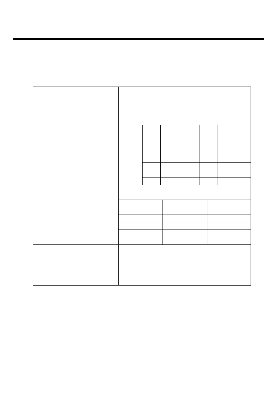
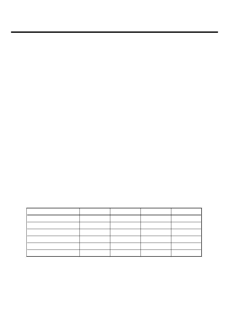
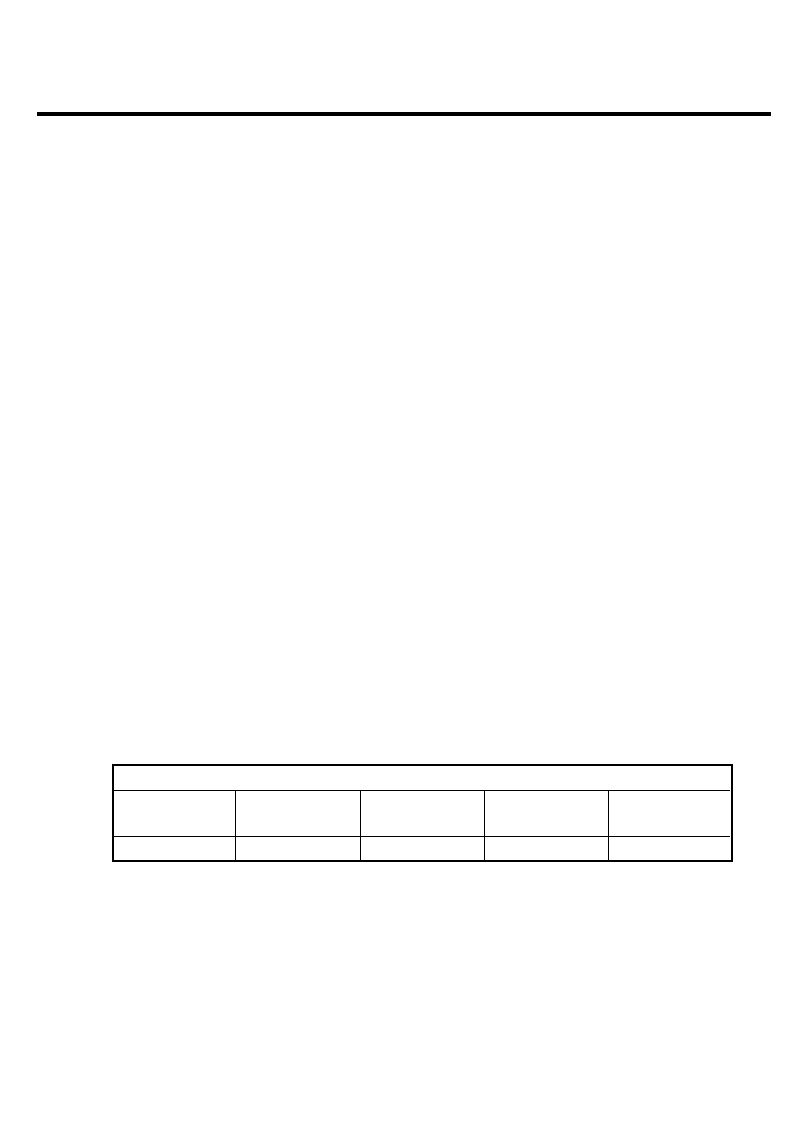
2.1 System Overview
2. PERFORMANCE
Item
Specification
Shape
GSM900/1800/1900 and WCDMA2100 - Bar type Handset
Size
103.5 X 54.4 X 14.8 mm
Weight
Under 112 g (with 1000mAh Battery)
Power
3.7 V normal, 1000 mAh Li-Ion
Talk Time
Over 170 min (WCDMA, Tx=10 dBm, Voice)
with 1000mAh)
Over 200 min (GSM, Max Tx-29dBm, Voice)
Standby Time
Over 250 Hrs (WCDMA, DRX=1.28)
(with 1000mAh)
Over 250 Hrs (GSM, Paging period=5)
Antenna Internal
type
LCD
Main 3” TFT, WQVGA, 262K
LCD Backlight
White LED Back Light
Camera
5.0 Mega pixel + VGA Video Call Camera
Vibrator
Yes (Coin Type)
LED Indicator
No
MIC Yes
Receiver Yes
Earphone Jack
Yes (18 pin)
Connectivity Bluetooth,
USB
External Memory
Yes(Micro SD)
I/O Connect
18 Pin
LGE Internal Use Only
Copyright © 2007 LG Electronics. Inc. All right reserved.
Only for training and service purposes
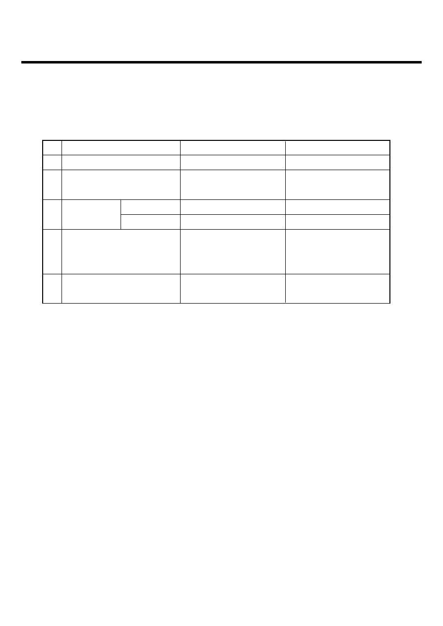
2.2 Usable environment
1) Environment
2) Environment (Accessory)
* CLA : 12 ~ 24 V(DC)
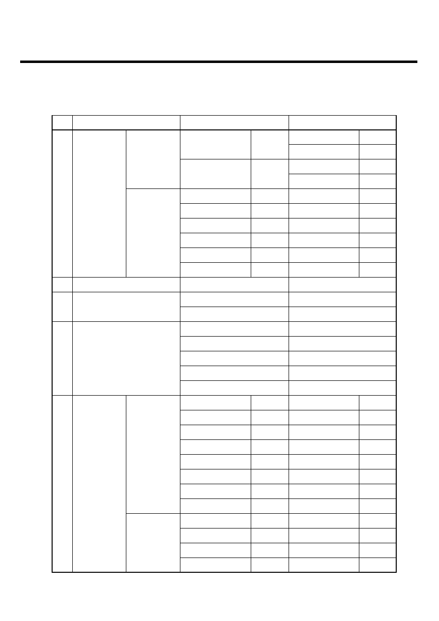
2.3 Radio Performance
1) Transmitter - GSM Mode
* In case of DCS : [A] -> 1710, [B] -> 1785
* In case of PCS : [A] -> 1850, [B] -> 1910
2. PERFORMANCE
- 8 -
Item
Specification
Voltage
3.7 V(Typ), 3.2 V(Min), [Shut Down : 3.2 V]
Operation Temp
-20 ~ +60
°C
Storage Temp
-30 ~ +80
°C
Humidity
85 % (Max)
Reference
Spec.
Min
Typ.
Max
Unit
TA Power
Available power
100
220
240
Vac
No
Item
GSM
DCS & PCS
100k~1GHz
-39dBm
9k ~ 1GHz
-39dBm
MS allocated
1G~[A]MHz
-33dBm
Channel
1G~12.75GHz
-33dBm
[A]M~[B]MHz
-39dBm
Conducted
[B]M~12.75GHz
-33dBm
1
Spurious
100k~880MHz
-60dBm
100k~880MHz
-60dBm
Emission
880M~915MHz
-62dBm
880M~915MHz
-62dBm
Idle Mode
915M~1GHz
-60dBm
915M~1GHz
-60dBm
1G~[A]MHz
-50dBm
1G~[A]MHz
-50dBm
[A]M~[B]MHz
-56dBm
[A]M~[B]MHz
-56dBm
[B]M~12.5GHz
-50dBm
[B]M~12.5GHz
-50dBm
LGE Internal Use Only
Copyright © 2007 LG Electronics. Inc. All right reserved.
Only for training and service purposes
2. PERFORMANCE
- 9 -
** In case of DCS : [A] -> 1710, [B] -> 1785
* In case of PCS : [A] -> 1850, [B] -> 1910
No
Item
GSM
DCS & PCS
30M ~ 1GHz
-36dBm
30M~1GHz
-36dBm
MS allocated
1G~[A]MHz
-30dBm
Channel
1G ~ 4GHz
-30dBm
[A]M~[B]MHz
-36dBm
Radiated
[B]M~4GHz
-30dBm
2
Spurious
30M ~ 880MHz
-57dBm
30M~880MHz
-57dBm
Emission
880M ~ 915MHz
-59dBm
880M~915MHz
-59dBm
Idle Mode
915M~1GHz
-57dBm
915M~1GHz
-57dBm
1G~[A]MHz
-47dBm
1G~[A]MHz
-47dBm
[A]M~[B]MHz
-53dBm
[A]M~[B]MHz
-53dBm
[B]M~4GHz
-47dBm
[B]M~4GHz
-47dBm
3
Frequency Error
±0.1ppm
±0.1ppm
4
Phase Error
±5(RMS)
±5(RMS)
±20(PEAK)
±20(PEAK)
3dB below reference sensitivity
3dB below reference sensitivity
Frequency Error
RA250 : ±200Hz
RA250: ±250Hz
5
Under Multipath and
HT100 : ±100Hz
HT100: ±250Hz
Interference Condition
TU50 : ±100Hz
TU50: ±150Hz
TU3 : ±150Hz
TU1.5: ±200Hz
0 ~ 100kHz
+0.5dB
0 ~ 100kHz
+0.5dB
200kHz
-30dB
200kHz
-30dB
250kHz
-33dB
250kHz
-33dB
Due to
400kHz
-60dB
400kHz
-60dB
Output RF
modulation
600 ~ 1800kHz
-66dB
600 ~ 1800kHz
-60dB
6
1800 ~ 3000kHz
-69dB
1800 ~ 6000kHz
-65dB
Spectrum
3000 ~ 6000kHz
-71dB
≥6000kHz
-73dB
≥6000kHz
-77dB
Due to
400kHz
-19dB
400kHz
-22dB
Switching
600kHz
-21dB
600kHz
-24dB
transient
1200kHz
-21dB
1200kHz
-24dB
1800kHz
-24dB
1800kHz
-27dB
LGE Internal Use Only
Copyright © 2007 LG Electronics. Inc. All right reserved.
Only for training and service purposes
2. PERFORMANCE
- 10 -
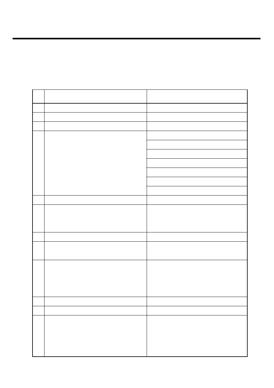
No
Item
GSM
DCS & PCS
Frequency offset
800kHz
7
Intermodulation attenuation
–
Intermodulation product should
be Less than 55dB below the
level of Wanted signal
Power control Power Tolerance Power control Power Tolerance
Level
(dBm)
(dB)
Level
(dBm)
(dB)
5
33
±3
0
30
±3
6
31
±3
1
28
±3
7
29
±3
2
26
±3
8
27
±3
3
24
±3
9
25
±3
4
22
±3
10
23
±3
5
20
±3
8
Transmitter Output Power
11
21
±3
6
18
±3
12
19
±3
7
16
±3
13
17
±3
8
14
±3
14
15
±3
9
12
±4
15
13
±3
10
10
±4
16
11
±5
11
8
±4
17
9
±5
12
6
±4
18
7
±5
13
4
±4
19
5
±5
14
2
±5
15
0
±5
9
Burst timing
Mask IN
Mask IN
LGE Internal Use Only
Copyright © 2007 LG Electronics. Inc. All right reserved.
Only for training and service purposes
2. PERFORMANCE
- 11 -
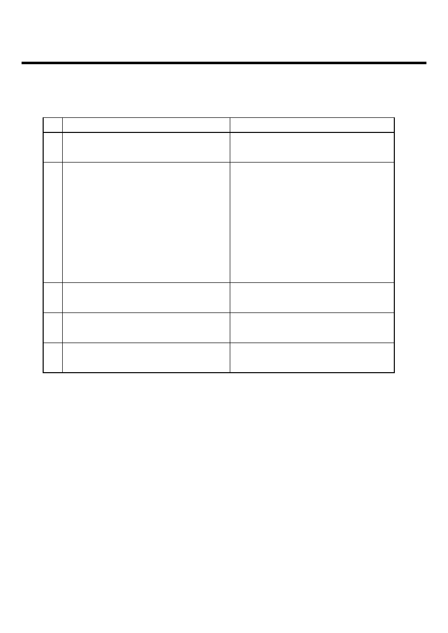
2) Transmitter - WCDMA Mode
No
Item
Specification
1
Maximum Output Power
Class 3 : +24dBm(+1/-3dB)
2
Frequency Error
±0.1ppm
3
Open Loop Power control in uplink
±9dB@normal, ±12dB@extreme
Adjust output(TPC command)
cmd 1dB 2dB 3dB
+1 +0.5/1.5 +1/3 +1.5/4.5
4
Inner Loop Power control in uplink
0 -0.5/+0.5 -0.5/+0.5 -0.5/+0.5
-1 -0.5/-1.5 -1/-3 -1.5/-4.5
Group (10 equel command group)
+1 +8/+12 +16/+24
5
Minimum Output Power
-50dBm(3.84MHz)
Qin/Qout : PCCH quality levels
6
Out-of-synchronization handling of output power
Toff@DPCCH/Ior : -22 -> -28dB
Ton@DPCCH/Ior : -24 -> -18dB
7
Transmit OFF Power
-56dBm(3.84MHz)
8
Transmit ON/OFF Time Mask
±25us
PRACH,CPCH,uplinlk compressed mode
±25us
9
Change of TFC
Power varies according to the data rate
DTX : DPCH off
(minimize interference between UE)
10
Power setting in uplink compressed
±3dB(after 14slots transmission gap)
11
Occupied Bandwidth(OBW)
5MHz(99%)
-35-15*(∆f-2.5)dBc@∆f=2.5~3.5MHz,30k
12
Spectrum emission Mask
-35-1*(∆f-3.5)dBc@∆f=3.5~7.5MHz,1M
-39-10*(∆f-7.5)dBc@∆f=7.5~8.5MHz,1M
-49dBc@∆f=8.5~12.5MHz,1M
LGE Internal Use Only
Copyright © 2007 LG Electronics. Inc. All right reserved.
Only for training and service purposes
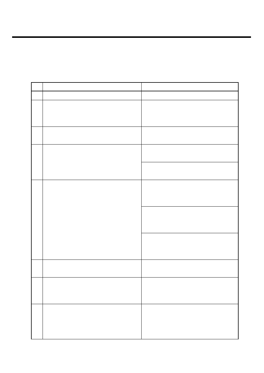
3)Receiver - GSM Mode
2. PERFORMANCE
- 12 -
No
Item
Specification
13
Adjacent Channel Leakage Ratio(ACLR)
33dB@5MHz, ACP>-50dBm
43dB@10MHz, ACP>-50dBm
-36dBm@f=9~150KHz, 1K BW
-36dBm@f=50KHz~30MHz, 10K BW
-36dBm@f=30MHz~1000MHz, 100K BW
14
Spurious Emissions
-30dBm@f=1~12.5GHz, 1M BW
(*: additional requirement)
(*)-41dBm@f=1893.5~1919.6MHz, 300K
(*)-67dBm@f=925~935MHz, 100K BW
(*)-79dBm@f=935~960MHz, 100K BW
(*)-71dBm@f=1805~1880MHz, 100K BW
15
Transmit Intermodulation
-31dBc@5MHz,Interferer -40dBc
-41dBc@10MHz, Interferer -40dBc
16
Error Vector Magnitude (EVM)
17.5%(>-20dBm)
(@12.2K, 1DPDCH+1DPCCH)
17
Transmit OFF Power
-15dB@SF=4.768Kbps, Multi-code
transmission
LGE Internal Use Only
Copyright © 2007 LG Electronics. Inc. All right reserved.
Only for training and service purposes
2. PERFORMANCE
- 13 -
3) Transmitter - HSDPA Mode
No
Item
Specification
1
Maximum Output Power
Sub-Test
1=1/15,
2=12/15
21~25dBm / 3.84 MHz
3=13/15
4=15/8
20~25dBm / 3.84 MHz
5=15/7
6=15/0
19~25dBm / 3.84 MHz
Sub-test
Power Start of Ack/Nack Power
Transmitter
in table
step
boundary
step
power step
C.10.1.4
size, P tolerance
2
HS-DPCCH
[dB]
[dB]
1
Start of Ack/Nack 6
+/- 2.3
5
2
Start of CQI
1
+/- 0.6
3
Middle of CQI
0
+/- 0.6
4
End of CQI
5
+/- 2.3
3
Spectrum Emission Mask
Sub-Test : 1=1/15, 2=12/15, 3=13/15,
4=15/8, 5=15/7, 6=15/0
Frequency offset
Minimum
Measurement
from carrier ∆f
requirement
Bandwidth
2.5 ~ 3.5 MHz
-35-15(∆f-2.5)dBc
30 kHz
3.5 ~ 7.5 MHz
-35-1(∆f-3.5)dBc
1 MHz
7.5 ~ 8.5 MHz
-35-10(∆f-7.5)dBc
1 MHz
8.5 ~ 12.5 MHz
-49dBc
1 MHz
4
Adjacent Channel Leakage
Sub-Test : 1=1/15, 2=12/15, 3=13/15,
Power Ratio (ACLR)
4=15/8, 5=15/7, 6=15/0
> 33 dB @ ±5 MHz
> 43 dB @ ±10 MHz
5
Error Vector Magnitude
3GPP Not Complete
- 14 -
2. PERFORMANCE
4)Receiver - GSM Mode
LGE Internal Use Only
Copyright © 2007 LG Electronics. Inc. All right reserved.
Only for training and service purposes
No
Item
GSM
DCS & PCS
1
Sensitivity (TCH/FS Class II)
-105dBm
-105dBm
2
Co-Channel Rejection
C/Ic=7dB
Storage -30 ~ +85
(TCH/FS Class II, RBER, TU high/FH)
3
Adjacent Channel
200kHz
C/Ia1=-12dB
C/Ia1=-12dB
Rejection
400kHz
C/Ia2=-44dB
C/Ia2=-44dB
Wanted Signal :-98dBm 1st
Wanted Signal :-96dBm 1st
4
Intermodulation Rejection
interferer:-44dBm 2nd
interferer:-44dBm 2nd
interferer:-45dBm
interferer:-44dBm
5
Blocking Response
Wanted Signal :-101dBm
Wanted Signal :-101dBm
(TCH/FS Class II, RBER)
Unwanted : Depend on Frequency
Unwanted : Depend on Frequency
- 15 -
2. PERFORMANCE
LGE Internal Use Only
Copyright © 2007 LG Electronics. Inc. All right reserved.
Only for training and service purposes
5) Receiver - WCDMA Mode
No
Item
Specification
1
Reference Sensitivity Level
-106.7 dBm(3.84 MHz)
-25dBm(3.84MHz)
2
Maximum Input Level
-44dBm/3.84MHz(DPCH_Ec)
UE@+20dBm output power(Class3)
3
Adjacent Channel Selectivity (ACS)
33dB
UE@+20dBm output power(Class3)
-56dBm/3.84MHz@10MHz
4
In-band Blocking
UE@+20dBm output power(Class3)
-44dBm/3.84MHz@15MHz
UE@+20dBm output power(Class3)
-44dBm/3.84MHz@f=2050~2095 and
2185~2230MHz
UE@+20dBm output power(Class3)
-30dBm/3.84MHz@f=2025~2050 and
5
Out-band Blocking
2230~2255MHz
UE@+20dBm output power(Class3)
-15dBm/3.84MHz@f=1~2025 and
2255~12500MHz
UE@+20dBm output power(Class3)
6
Spurious Response
-44dBm CW
UE@+20dBm output power(Class3)
-46dBm CW@10MHz
7
Intermodulation Characteristic
-46dBm/3.84MHz@20MHz
UE@+20dBm output power(Class3)
-57dBm@f=9KHz~1GHz, 100K BW
8
Spurious Emissions
-47dBm@f=1~12.5GHz, 1M BW
-60dBm@f=1920MHz~1980MHz, 3.84M BW
-60dBm@f=2110MHz~2170MHz, 3.84M BW
LGE Internal Use Only
Copyright © 2007 LG Electronics. Inc. All right reserved.
Only for training and service purposes
2. PERFORMANCE
- 16 -
6) Receiver - HSDPA Mode
2.4 Current Consumption
1) KU990/U990 Current Consumption
(Stand by and Voice Call Test Condition : Bluetooth off, LCD backlight off,Neighbor Cell off) (VT Test
Condition : Speaker off, LCD backlight On)
Stand by
Voice Call
VT
WCDMA
Under 4.00 mA
Under 350 mA
Under 550mA
(DRX=1.28)
(Tx=10dBm)
(Tx=10dBm)
Under 4.00 mA
Under 300 mA
GSM
Paging=5 period
(Tx=29dBm)
No Item
Specification
1
Maximum Input Level
Sub-Test : 1=1/15, 2=12/15, 3=13/15,
(BLER or R), 16QAM Only
4=15/8, 5=15/7, 6=15/0
BLER < 10% or R >= 700kbps
LGE Internal Use Only
Copyright © 2007 LG Electronics. Inc. All right reserved.
Only for training and service purposes
2.5 RSSI BAR
2.6 Battery BAR
2. PERFORMANCE
- 17 -
Indication
Standby
Bar 4
Over 3.81
± 0.03V
Bar 4
→ 3
3.80
± 0.03V
Bar 3
→ 2
3.70
± 0.03V
Bar 2
→ 1
3.61
± 0.03V
Bar 1
→ Empty
3.49
± 0.03V
Low Voltage,
3.49
± 0.03V (Stand-by) / 3.49 ± 0.03V (Talk)
Warning message+ Blinking
[Interval : 3min(Stand-by) / 1min(Talk)]
Power Off
3.20
± 0.03V (Stand-by)
3.10
± 0.03V (Talk)
Level Change
WCDMA
GSM
BAR 4
→ 3
-88
± 2 dBm
-90
± 2 dBm
BAR 3
→ 2
-98
± 2 dBm
-95
± 2 dBm
BAR 2
→ 1
-108
± 2 dBm
-100
± 2 dBm
BAR 1
→ 0
-112
± 2 dBm
-106
± 2 dBm
LGE Internal Use Only
Copyright © 2007 LG Electronics. Inc. All right reserved.
Only for training and service purposes
2. PERFORMANCE
- 18 -
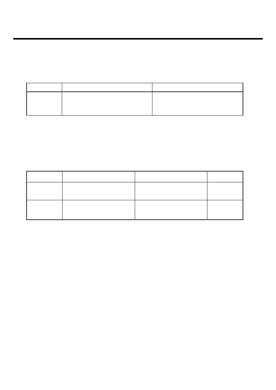
2.7 Sound Pressure Level
2.8 Charging
• Charging Method : CC & CV (Constant Current and Constant Voltage)
• Maximum Charging Voltage : 4.2 V
• Maximum Charging Current : 600 mA
• Normal Battery Capacity : 1000 mAh
• Charging Time : Max 3 hours (except for trickle charging time)
• Full charging indication current (charging icon stop current) : 80 mA
• Cut-off voltage : 3.20 V (Stand-By), 3.10V (Talk)
No
Test Item
Specification
1
Sending Loudness Rating (SLR)
8 ±3 dB
2
Receiving Loudness Rating (RLR)
Nor
-4 ± 3 dB
Max
-15 ± 3 dB
3
Side Tone Masking Rating (STMR)
Min
17 dB
4
Echo Loss (EL)
Min
40 dB
5
Idle Noise-Sending (INS)
Max
-64 dBm0p
6
Idle Noise-Receiving (INR)
Nor
Under -47 dBPA
Max
Under -36 dBPA
7
Sending Loudness Rating (SLR)
8±3dB
8
Receiving Loudness Rating (RLR)
Nor
-1 ±3 dB
Max
-12 ±3 dB
9
Side Tone Masking Rating (STMR)
Min
25 dB
10
Echo Loss (EL)
Min
40 dB
11
Idle Noise-Sending (INS)
Max
-55 dBm0p
12
Idle Noise-Receiving (INR)
Nor
Under -45 dBPA
Max
Under -40 dBPA
TDMA Noise
-. GSM : Power Level : 5
DCS/PCS : Power Level : 0
(Cell Power : -90 ~ -105 dBm)
13
-. Acoustic (Max Vol.)
MS/Headset SLR : 8 ± 3dB
MS/Headset RLR : -15 ± 3dB/-12dB
(SLR/RLR : Mid-value setting)
MS
Headset
MS and
Headset
Max
Under -62 dBm
LGE Internal Use Only
Copyright © 2007 LG Electronics. Inc. All right reserved.
Only for training and service purposes
3. TECHNICAL BRIEF
- 19 -
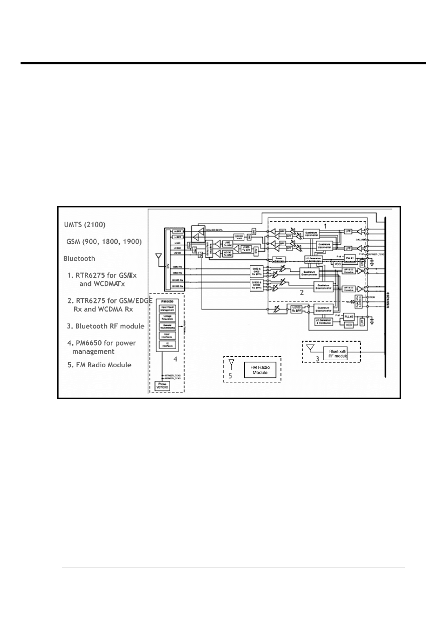
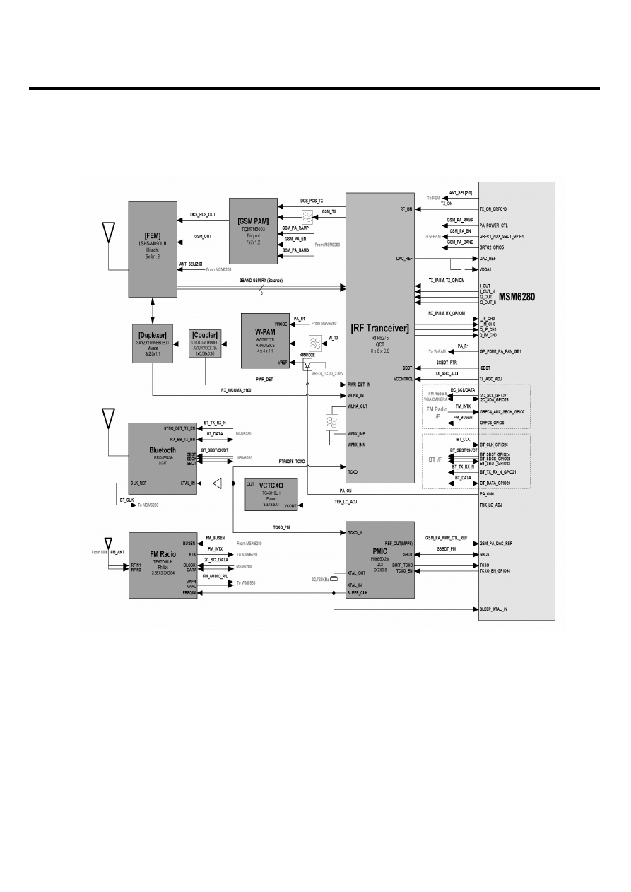
3.1 General Description
The U990 supports UMTS-2100, GSM-900, DCS-1800, and PCS-1900 based
GSM/GPRS/EDGE/UMTS. All receivers and the UMTS transmitter use the radioOne
1
Zero-IF
architecture to eliminate intermediate frequencies, directly converting signals between RF and
baseband. The quad-band GSM transmitters use a baseband-to-IF upconversion followed by an offset
phase-locked loop that translates the GMSK-modulated or 8-PSK-modulated signal to RF.
1
QUALCOMM’s branded chipset that implements a Zero-IF radio architecture.
3. TECHNICAL BRIEF
[Fig 1.1] Block diagram of RF part

LGE Internal Use Only
Copyright © 2007 LG Electronics. Inc. All right reserved.
Only for training and service purposes
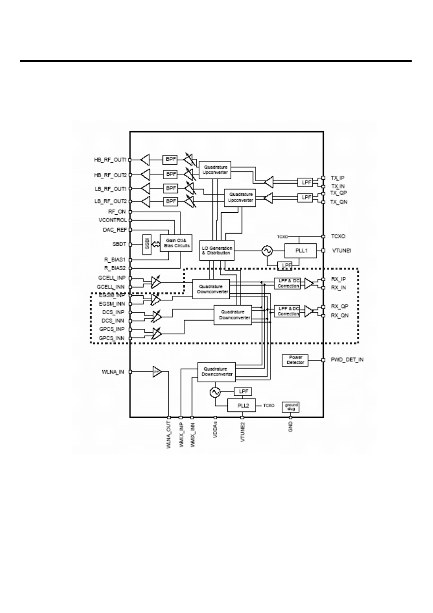
A generic, high-level functional block diagram of U990 is shown in Figure 1-1. One antenna collects
base station forward link signals and radiates handset reverse link signals. The antenna connects with
receive and transmit paths through a FEM(Front End Module).
The UMTS receive paths each include an LNA, an RF band-pass filter, and a downconverter that
translate the signal directly from RF-to-baseband using radioOne ZIF techniques. The RFIC’s Rx
analog baseband outputs, for the receive chains, connect to the MSM IC. The UMTS and GSM Rx
baseband outputs share the same inputs to the MSM IC.
For the transmit chains, the RTR6275 IC directly translates the Tx baseband signals (from the MSM
device) to an RF signal using an internal LO generated by integrated on-chip PLL and VCO. The
RTR6275 IC outputs deliver fairly high-level RF signals that are first filtered by Tx SAWs and then
amplified by their respective UMTS PAs. The high- and low-band UMTS RF transmit signals emerge
from the RTR6275 transceiver.
In the GSM receive path, the received RF signals are applied through their band-pass filters and
down-converted directly to baseband in the RTR6275 transceiver IC. These baseband outputs are
shared with the UMTS receiver and routed to the MSM IC for further signal processing.
The GSM/EDGE transmit path employs one stage of up-conversion and, in order to improve efficiency,
is divided into phase and amplitude components to produce an open-loop Polar topology:
1. The on-chip quadrature up-converter translates the GMSK-modulated signal or 8-PSK modulated
signal, to a constant envelope phase signal at RF;
2. The amplitude-modulated (AM) component is applied to the ramping control pin of Polar power
amplifier from a DAC within the MSM
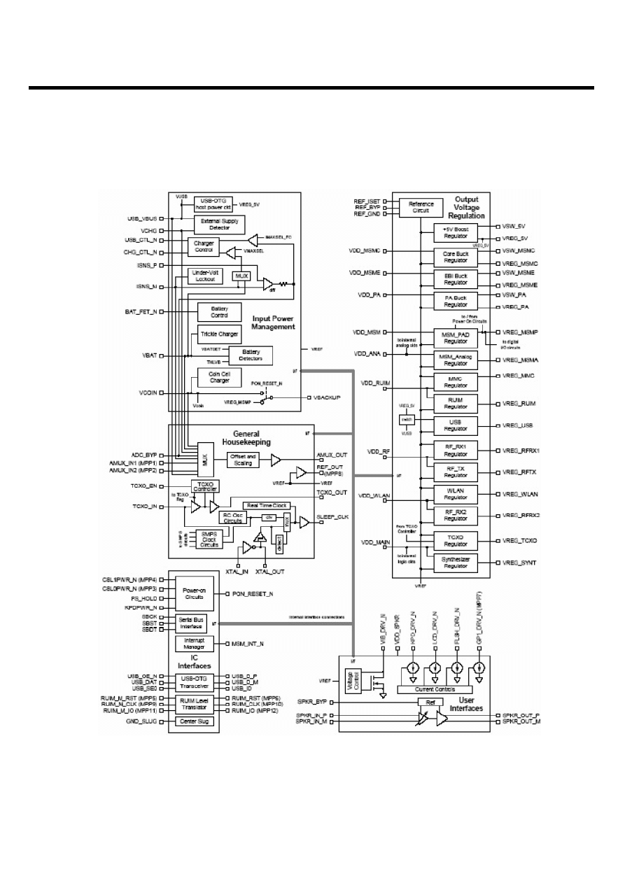
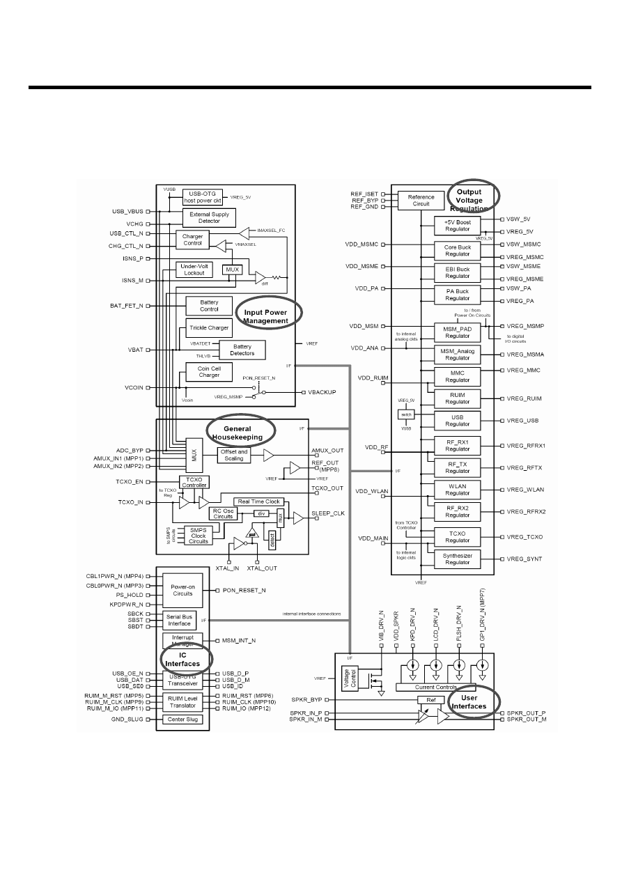
U990 power supply voltages are managed and regulated by the PM6650 Power Management IC. This
versatile device integrates all wireless handset power management, general housekeeping, and user
interface support functions into a single mixed signal IC. It monitors and controls the external power
source and coordinates battery recharging while maintaining the handset supply voltages using low
dropout, programmable regulators.
The device’s general housekeeping functions include an ADC and analog multiplexer circuit for
monitoring on-chip voltage sources, charging status, and current flow, as well as userdefined off-chip
variables such as temperature, RF output power, and battery ID. Various oscillator, clock, and counter
circuits support IC and higher-level handset functions. Key parameters such as under-voltage lockout
and crystal oscillator signal presence are monitored to protect against detrimental conditions.
3. TECHNICAL BRIEF
- 20 -
LGE Internal Use Only
Copyright © 2007 LG Electronics. Inc. All right reserved.
Only for training and service purposes
3. TECHNICAL BRIEF
- 21 -
3.2 GSM Mode
3.2.1 GSM Receiver
The Dual-mode U990’s receiver functions are split between the three RFICs as follows:
• GSM-900, DCS-1800, PCS-1900 and UMTS-2100 modes both use the RTR6275 IC only. Each
mode has independent front-end circuits and down-converters, but they share common baseband
circuits (with only one mode active at a time). All receiver control functions are beginning with SBI2-
controlled parameters.
RF Front end consists of antenna, antenna switch module (LSHS-M090UH) which includes three RX
saw filters (GSM-900, DCS-1800 and PCS-1900). The antenna switch module allows multiple
operating bands and modes to share the same antenna. In U990, a common antenna connects to one
of six paths: 1) UMTS-2100 Rx/Tx, 2) GSM-900 Rx, 3) GSM-900 Tx, 4) DCS-1800 Rx, and 5) DCS-
1800, PCS-1900 Tx(High Band Tx’s share the same path), 6) PCS-1900 Rx. UMTS operation requires
simultaneous reception and transmission, so the UMTS Rx/Tx connection is routed to a duplexer that
separates receive and transmit signals. GSM900, DCS1800, and PCS1900 operation is time division
duplexed, so only the receiver or transmitter is active at any time and a frequency duplexer is not
required.
Control Logic (L : 0 ~ 0.1V, H : 2.6 ~ 2.8V)
L/H : L and H are acceptable
2
The RFIC operating modes and circuit parameters are MSM-controlled through the proprietary 3-line Serial Bus Interface (SBI). The Application
Programming Interface (API) is used to implement SBI commands. The API is documented in AMSS Software - please see applicable AMSS
Software documentation for details.
Vc3
Vc2
Vc1
Vdd
GSM900 Tx
L
H
H
H
DCS1800/PCS1900 Tx
L
L
H
H
UMTS Tx/Rx
H
L
H
H
GSM 900 Rx
L
L/H
L
H
DCS 1800 Rx
H
L/H
L
H
PCS 1900 Rx
L
L/H
L
H
[Table 1.1] Antenna Switch Module Control logic

LGE Internal Use Only
Copyright © 2007 LG Electronics. Inc. All right reserved.
Only for training and service purposes
The GSM900, DCS1800, and PCS1900 receiver inputs of RTR6275 are connected directly to the
transceiver front-end circuits(filters and antenna switch module). GSM900, DCS1800, and PCS1900
receiver inputs use differential configurations to improve common-mode rejection and second-order
non-linearity performance. The balance between the complementary signals is critical and must be
maintained from the RF filter outputs all the way into the IC pins
Since GSM900, DCS1800, and PCS1900 signals are time-division duplex (the handset can only
receive or transmit at one time), switches are used to separate Rx and Tx signals in place of frequency
duplexers - this is accomplished in the switch module.
The GSM900, DCS1800, and PCS1900 receive signals are routed to the RTR6275 through band
selection filters and matching networks that transform single-ended 50-Ωsources to differential
impedances optimized for gain and noise figure. The RTR input uses a differential configuration to
improve second-order inter-modulation and common mode rejection performance. The RTR6275 input
stages include MSM-controlled gain adjustments that maximize receiver dynamic range.
The amplifier outputs drive the RF ports of the quadrature RF-to-baseband downconverters. The
downconverted baseband outputs are multiplexed and routed to lowpass filters (one I and one Q)
having passband and stopband characteristics suitable for GMSK or 8-PSK processing. These filter
circuits include DC offset corrections. The filter outputs are buffered and passed on to the MSM6280 IC
for further processing (an interface shared with the RFR6275 UMTS receiver outputs)
3. TECHNICAL BRIEF
- 22 -
LGE Internal Use Only
Copyright © 2007 LG Electronics. Inc. All right reserved.
Only for training and service purposes
3. TECHNICAL BRIEF
- 23 -
[Fig 1.2] RTR6275 RX feature
LGE Internal Use Only
Copyright © 2007 LG Electronics. Inc. All right reserved.
Only for training and service purposes
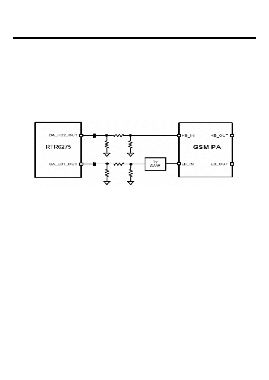
3.2.2 GSM Transmitter
The RTR6275 transmitter outputs(DA_HB2_OUT and DA_LB1_OUT) include on-chip output matching
inductors. 50ohm output impedance is achieved by adding a series capacitor at the output pins. The
capacitor value may be optimized for specific applications and PCB characteristics based on pass-band
symmetry about the band center frequency, the suggested starting value is shown in Figure1.3.
The RTR6275 IC is able to support GSM 900 and GSM 1800/1900 mode transmitting. This design
guideline shows a tri-band GSM application.
Both high-band and low band outputs are followed by resistive pads to ensure that the load Presented
to the outputs remains close to 50ohm. The low-band GSM. Tx path also includes a Tx-band SAW filter
to remove noise-spurious components and noise that would be amplified by the PA and appear in the
GSM Rx band
3. TECHNICAL BRIEF
- 24 -
91Ω
91Ω
6pF
120Ω
120Ω
68Ω
5pF
51Ω
[Fig 1.3] GSM Transmitter matching

LGE Internal Use Only
Copyright © 2007 LG Electronics. Inc. All right reserved.
Only for training and service purposes
3. TECHNICAL BRIEF
- 25 -
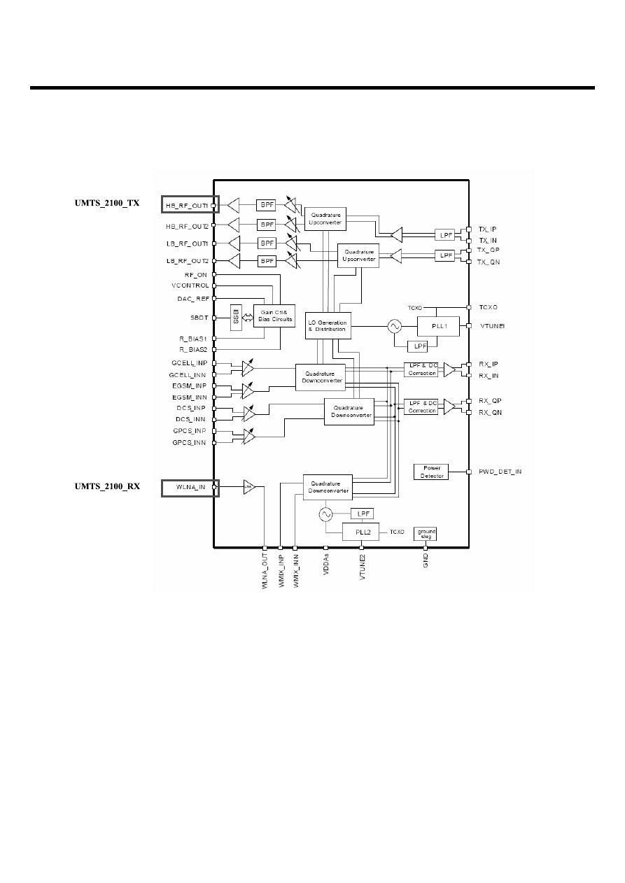
3.3 UMTS Mode
3.3.1 Receiver
The UMTS duplexer receiver output is routed to LNA circuits within the RTR6275 device. The UMTS Rx
input is provided with an on-chip LNA that amplifies the signal before a second stage filter that provides
differential downconverter. This second stage input is configured differentially to optimize second-order
intermodulation and common mode rejection performance. The gain of the UMTS frontend amplifier and
the UMTS second stage differential amplifier are adjustable, under MSM control, to extend the dynamic
range of the receivers. The second stage UMTS Rx amplifiers drive the RF ports of the quadrature RF-
tobaseband downconverters. The downconverted UMTS Rx baseband outputs are routed to lowpass
filters having passband and stopband characteristics suitable for UMTS Rx processing. These filter
circuits allow DC offset corrections, and their differential outputs are buffered to interface shared with
GSM Rx to the MSM IC. The UMTS baseband outputs are turned off when the RTR6275 is
downconverting GSM signals and on when the UMTS is operating.
3.3.2 Transmitter
The UMTS Tx path begins with differential baseband signals (I and Q) from the MSM device. These
analog input signals are amplified, filtered, and applied to the quadrature up-converter mixers. The up-
converter output is amplified by multiple variable gain stages that provide transmit AGC control. The
AGC output is filtered and applied to the driver amplifier; this output stage includes an integrated
matching inductor that simplifies the external matching network to a single series capacitor to achieve
the desired 50-Ω interface.
The RTR6275 UMTS output is routed to its power amplifier through a bandpass filter, and delivers fairly
high-level signals that are filtered and applied to the PA. Transmit power is delivered from the duplexer
to the antenna through the switch module.
The transceiver LO synthesizer is contained within the RTR6275 IC with the exception of the off-chip
loop filter components and the VC-TCXO. This provides a simplified design for multimode applications.
The PLL circuits include a reference divider, phase detector, charge pump, feedback divider, and digital
logic generator.
UMTS Tx. Using only PLL1, the LO generation and distribution circuits create the necessary LO signals
for nine different frequency converters. The UMTS transmitter also employs the ZIF architecture to
translate the signal directly from baseband to RF. This requires FLO to equal FRF, and the RTR6275 IC
design achieves this without allowing FVCO to equal FRF. The RTR6275 IC is able to support UMTS
2100/1900 and UMTS 850 mode transmitting.
This design guideline shows only UMTS 2100 applications.
LGE Internal Use Only
Copyright © 2007 LG Electronics. Inc. All right reserved.
Only for training and service purposes
3. TECHNICAL BRIEF
- 26 -
[Figure 1.4] RTR6275 IC functional block diagram
LGE Internal Use Only
Copyright © 2007 LG Electronics. Inc. All right reserved.
Only for training and service purposes
3.4 LO generation and distribution circuits
The integrated LO generation and distribution circuits are driven by internal VCOs to support various
modes to yield highly flexible quadrature LO outputs that drive all GSM/EDGE and UMTS band
upconverters and downconverters; with the help of these LO generation and distribution circuits, true
zero-IF architecture is employed in all GSM and UMTS band receivers and transmitters to translate the
signal directly from RF to baseband and from baseband to RF.
Two fully functional fractional-N synthesizers, including VCOs and loop filters, are integrated within the
RTR6275 IC. The first synthesizer (PLL1) creates the transceiver LOs that support the UMTS
2100/1900/1800 transmitter, and all four GSM band receivers and transmitters including: GSM850,
GSM900, DCS1800, and PCS1900. The second synthesizer (PLL2) provides the LO for the UMTS
2100/1900/1800 receiver. An external TCXO input signal is required to provide the synthesizer
frequency reference to which the PLL is phase and frequency locked. The RTR6275 IC integrates
most of PLL loop filter components onchip except two off-chip loop filter series capacitors, and
significantly reduces off-chip component requirement. With the integrated fractional-N PLL
synthesizers, the RTR6275 has the advantages of more flexible loop bandwidth control, fast lock time,
and low-integrated phase error.
3.5 Off-chip RF Components
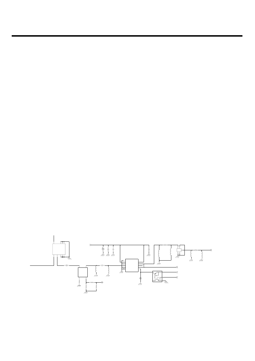
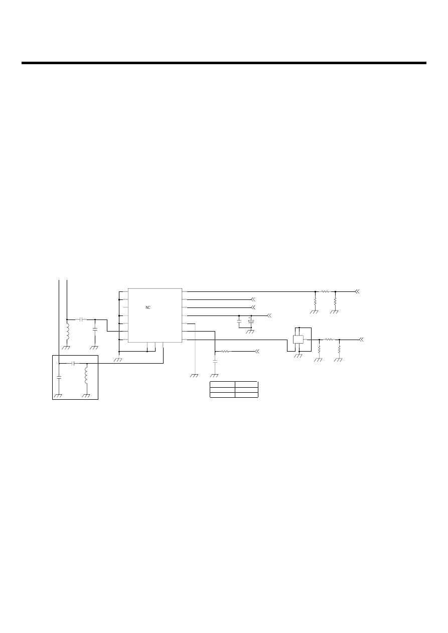
3.5.1 UMTS PAM (U105: AWT6277R)
The UMTS PA output power is monitored by power detector circuits (U101 : RTR6275) . This detector
voltage can be used for transmitter calibration and monitor to meet RF system specification.
3. TECHNICAL BRIEF
- 27 -
[Figure 1.5] UMTS PAM, Duplexer, Coupler
20dB
8 dB
NA
C165
100p
C163
C160
22u
51
R124
L122
NA
100
R126
2
4
5
3
1
Q100
KRX102E
C162
0.01u
15nH
L123
2
RFIN
RFOUT
8
VCC1
1
10
VCC2
4
VMODE
VREF
5
AWT6277R
U105
GND1
3
GND2
6
7
GND3
9
GND4
GND5
11
5.6p
C169
C161
56p
SCDY0003403
50OHM
4
3
COUP
2
IN
1
OUT
C173
100p
U104
R123
68
C159
8.2p
1.8p
C170
L128
4.7nH
L124
3.3nH
L126
8.2nH
EFCH1950TDF1
FL104
G1
2
G2
3
G3
5
IN
1
O1
4
R125
100
1u
C164
FL103
ANT
2
1
GND1
GND2
4
8
GND3
GND4
9
GND5
6
GND6
3
7
RX
5
TX
SAYZY1G95EB0B00
WCDMA_2100_TX_OUT
PA_ON
VREG_TCXO_2.85V
+VPWR
PA_R1
PWR_DET
LGE Internal Use Only
Copyright © 2007 LG Electronics. Inc. All right reserved.
Only for training and service purposes
3.5.2 VCTCXO (X100 : TG-5010LH(19.2M))
The Voltage Controlled Temperature Compensated Crystal Oscillator (VCTCXO) provides the
reference frequency for all RFIC synthesizers as well as clock generation functions within the
MSM6280 IC. The oscillator frequency is controlled by the MSM6280 IC.s TRK_LO_ADJ pulse density
modulated signal in the same manner as the transmit gain control TX_AGC_ADJ. A two-pole RC
lowpass filter is recommended on this control line.
The PM6650 IC controls the handset power-up sequence, including a special VCTCXO warm-up
interval before other circuits are turned on. This warm-up interval (as well as other TCXO controller
functions) is enabled by the MSM TCXO_EN line . The PM6650 IC VREG_TCXO regulated output
voltage is used to power the VCTCXO and is enabled before most other regulated outputs.
Any GSM mode power control circuits within the MSM6280 IC require a reference voltage for proper
operation and sufficient accuracy. Connecting the PM6650 IC REF_OUT directly to the MSM6275 IC
GSM_PA_PWR_CTL_REF provides this reference. This sensitive analog signal needs a 0.1 µF low
frequency filter near to MSM side, and isolate from digital logic and clock traces with ground on both
sides, plus ground above and below if routed on internal layers.
3.5.3 Front-End Module (FL100 : LSHS-M090UH)
This equipment uses a single antenna to support all handset operating modes, with an antenna switch
module select the operating frequency and band. UMTS operation requires simultaneous reception
and transmission, so the UMTS Rx/Tx connection is routed to a duplexer that separates receive and
transmit signals. The active connection is MSM-selected by three control lines (GPIO[9], GPIO[10],
and GPIO[11]). These GPIOs are programmed to be ANT_SEL0, ANT_SEL1, and ANT_SEL2
respectively.
3. TECHNICAL BRIEF
- 28 -
[Table 1.2] Front End Module control logic
Vc3
Vc2
Vc1
Vdd
GSM900 Tx
L
H
H
H
DCS1800/PCS1900 Tx
L
L
H
H
UMTS Tx/Rx
H
L
H
H
GSM 900 Rx
L
L
L
H
DCS 1800 Rx
H
L
L
H
PCS 1900 Rx
L
L
L
H

LGE Internal Use Only
Copyright © 2007 LG Electronics. Inc. All right reserved.
Only for training and service purposes
3. TECHNICAL BRIEF
- 29 -
3.5.4 PMIC Functional Block Diagram (U501 : PM6650-2M)
• Input power management
- Valid external supply attachment and removal detection
- Supports unregulated (closed-loop) external charger supplies and USB supplies as input power sources
- Supports lithium-ion main batteries
- Trickle, constant current, constant voltage, and pulsed charging of the main battery
- Supports coin cell backup battery (including charging)
- Battery voltage detectors with programmable thresholds
- VDD collapse protection
- Charger current regulation and real-time monitoring for over-current protection
- Charger transistor protection by power limit control
- Control drivers for two external pass transistors and one external battery MOSFET MOSFET is optional
- Voltage, current, and power control loops
- Automated recovery from sudden momentary power loss
• Output voltage regulation
- One boost (step-up) switched-mode power supply (SMPS) for driving white LEDs and hosting USBOTG
- Three buck (step-down) switched-mode power supplies that efficiently generate MSMC, MSME, and PA
(or second MSMC) supply voltages
- Supports dynamic voltage scaling (DVS) for MSMC and PA
- Eleven low dropout regulator circuits with programmable output voltages, implemented using three
different current ratings: 300 mA (two), 150 mA (six), and 50 mA (three). These can be used to power
MSMA, MSMP, RFRX1, RFRX2, RFTX, SYNT, TCXO, WLAN, MMC, USB, and RUIM circuits.
- All regulators can be individually enabled/disabled for power savings
- Low power mode available on MSMA and MSMP regulators
- All regulated outputs are derived from a common bandgap referenceclose tracking
• Integrated handset-level housekeeping functions reduces external parts count, size, cost
- Analog multiplexer selects from 8 internal and up to 18 external inputs
- Multiplexer outputs offset and gain are adjusted, increasing the effective ADC resolution
- Adjusted multiplexer output is buffered and routed to an MSM device ADC
- Dual oscillators -32.768 kHz off-chip crystal and on-chip RC assures MSM device sleep clock
- Crystal oscillator detector and automated switch-over upon lost oscillation
- Real time clock for tracking time and generating associated alarms
- On-chip adjustments minimize crystal oscillator frequency errors
- Circuits control TCXO warm-up and synchronize, deglitch, and buffer the TCXO signal
- TCXO buffer control for optimal QPH/catnap timing
- Three-stage over-temperature protection (smart thermal control)
• Integrated handset-level user interfaces
- Four programmable current sinks recommended as keypad backlight, LCD backlight,
camera flash, and general-purpose drivers
- Vibration motor driver programmable from 1.2 to 3.1V in 100 mV increments
- Speaker driver with programmable gain, turn-on time, and muting; differential operation
(drives external 8 Ω speakers with volume controlled 500 mW)

LGE Internal Use Only
Copyright © 2007 LG Electronics. Inc. All right reserved.
Only for training and service purposes
• IC-level interfaces
- MSM device-compatible 3-line SBI for efficient initialization, status, and control
- Supports the MSM devices interrupt processing with an internal interrupt manager
- Many functions monitored and reported through real-time and interrupt status signals
- Dedicated circuits for controlled power-on sequencing, including the MSM devices reset signal
- Several events continuously monitored for triggering power-on/power-off sequences
- Supports and orchestrates soft resets
- USB-OTG transceiver for full-speed (12 Mb/s) and low speed (1.5 Mb/s) interfacing of the MSM device to
computers as a USB peripheral, or connecting the MSM device to other peripherals
- RUIM level translators enable MSM device interfacing with external modules
• Twelve multi-purpose pins that can be configured as digital or analog I/Os, bi-directional I/Os, or current
sinks. Default functions support the RUIM level translators, power-on circuits, analog multiplexer inputs, an
LED driver, and a reference voltage buffer.
• Highly integrated functionality in a small package - 84-pin BCCS with a large center slug for electrical
ground, mechanical stability, and thermal relief
3. TECHNICAL BRIEF
- 30 -
LGE Internal Use Only
Copyright © 2007 LG Electronics. Inc. All right reserved.
Only for training and service purposes
3. TECHNICAL BRIEF
- 31 -
[Figure 1.7] PM6650 Block Diagram
LGE Internal Use Only
Copyright © 2007 LG Electronics. Inc. All right reserved.
Only for training and service purposes
3.5.5 GSM PAM (U101:TQM7M5003)
The TQM7M5003 is an extremely small (7 x 7 mm), GSM/EDGE PAM for handset applications. This
module has been optimized for excellent EDGE efficiency and Pout in a Polar Loop environment at
EDGE class E2+ operation while maintaining high GSM/GPRS efficiency.
The small size and high performance is achieved with high-reliability 3
rd
generation InGaP HBT
technology. With 50ߟ and output, no external matching or bias components are required.
The module incorporates two highly-integrated InGaP power amplifier die with a CMOS controller.
Each amplifier has three gain stages with on-die inter-stage matching implemented with a high Q
passives technology for optimal performance. The CMOS controller implements a fully integrated
power control within the module for GSM operations, and serves as the AM/AM path in EDGE
operations. This eliminates the need for any external couplers, power detectors, current sensing etc.,
to assure the output power level. The module has Tx enable and band select inputs. Module
construction is a low-profile overmolded landgrid array on laminate.
3. TECHNICAL BRIEF
- 32 -
[Figure 1. 8] GSM PAM Schematic
HIGH
MODE
LOW
GSM_PA_BAND
10 dB
GSM
DCS/PCS
PQ
8 dB
C138
NA
33u
C135
120
R119
120
R118
51
R114
91
R112
R117
2.2K
C142
0.75p
8p
C136
91
R113
1u
C137
L113
14
GND6
GND7
16
17
GND8
7
GSM_IN
9
GSM_OUT
3
TX_EN
VBATT
4
12
VCC
VRAMP
6
4.7nH
TQM7M5003
U101
2
BS
DCS_PCS_IN
1
DCS_PCS_OUT
15
5
GND1
GND2
8
10
GND3
11
GND4
13
GND5
2
G1
3
G2
5
G3
1
IN
4
O1
EFCH897MTDB1
FL101
15nH
L112
C146
10p
68p
C143
68
R111
GSM_PA_BAND
+VPWR
DCS_PCS_TX
GSM_TX
GSM_PA_RAMP
GSM_PA_EN

LGE Internal Use Only
Copyright © 2007 LG Electronics. Inc. All right reserved.
Only for training and service purposes
3. TECHNICAL BRIEF
- 33 -
3.5.6 UMTS Duplexer(FL103:SAYZY1G95EB0B00)
A UMTS duplexer splits a single operating band into receive and transmit paths. Important
performance requirements include;
• Insertion loss, this component is also in the receive and transmit paths ;
In the U990 typical losses : UMTS2100_ Tx = 1.5 dB, UMTS2100_ Rx = 1.8 dB
• Out-of-band rejection or attenuation, the duplexer provides input selectivity for the receiver, output
filtering for the transmitter, and isolation between the two. Rejection levels for both paths are
specified over a number of frequency ranges. Two Tx-to-Rx isolation levels are critical to receiver
performance:
• Rx-band isolation, the transmitter is specified for out-of-band noise falling into the Rx band. This
noise leaks from the transmit path into the receive path, and must be limited to avoid degrading
receiver sensitivity. The required Rx-band isolation depends on the PA out of-band noise levels and
Rx-band losses between the PA and LNA. Minimum duplexer Rx band isolation value is about 46.7
dB.
• Tx-band isolation, the transmit channel power also leaks into the receiver. In this case, the leakage is
outside the receiver passband but at a relatively high level. It combines with Rx band jammers to
create cross-modulation products that fall in-band to desensitize the receiver. The required Tx-band
isolation depends on the PA channel power and Tx-band losses between the PA and LNA. Minimum
duplexer Tx-band isolation value is about 51.7dB.
• Passband ripple, the loss of this fairly narrowband device is not flat across its passband. Passband
ripple increases the receive or transmit insertion loss at specific frequencies, creating performance
variations across the band.s channels, and should be controlled.
• Return loss, minimize mismatch losses with typical return losses of 10 dB or more (VSWR <2:1).
• Power handling, high power levels in the transmit path must be accommodated without degraded
performance. The specified level depends on the operating band class and mobile station class (per
the applicable standard), as well as circuit losses and antenna EIRP. Several duplexer characteristics
depend upon its source and load impedances. QUALCOMM strongly recommends an isolator be
used between the UMTS PA and duplexer to assure proper performance.
LGE Internal Use Only
Copyright © 2007 LG Electronics. Inc. All right reserved.
Only for training and service purposes
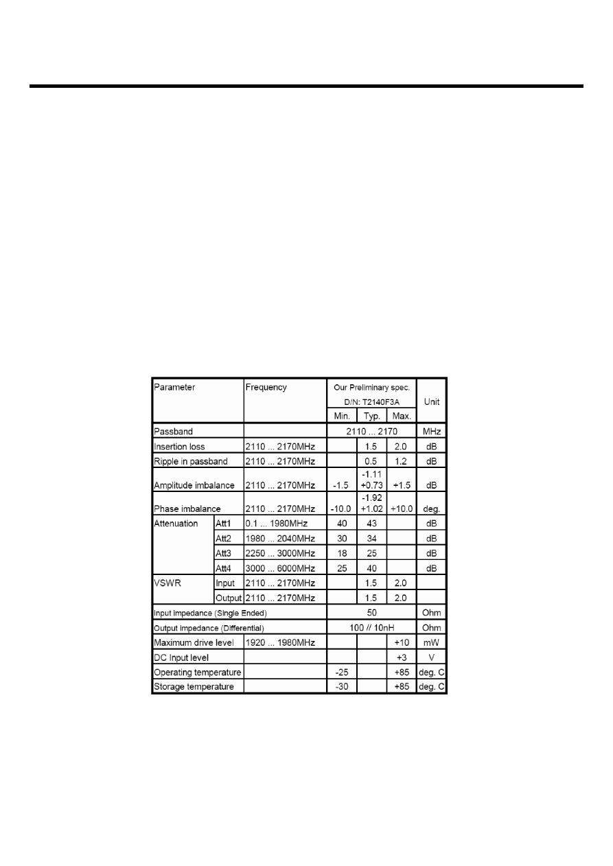
3.5.7 UMTS Rx RF filter (FL102 : EFCH2140TDE1)
An RF filter is located between the UMTS LNA and mixer. Insertion loss is important, but not as critical
as losses before the LNA. The most important parameters of this component include:
• Out-of-band rejection or attenuation levels, usually specified to meet these conditions:
- Far out-of-band signals - ranging from DC up to the first band of particular concern and from the
last band of particular concern to beyond three times the highest passband frequency.
- Tx-band leakage - the transmitter channel power, although attenuated by the duplexer, still
presents a cross-modulation threat in combination with Rx-band jammers. The RF filter must
provide rejection of this Tx-band leakage.
- Other frequencies of particular concern . bands known to include other wireless transmitters that
may deliver significant power levels to the receiver input.
3. TECHNICAL BRIEF
- 34 -
[Table 1.3] UMTS Rx SAW Filter Specification
LGE Internal Use Only
Copyright © 2007 LG Electronics. Inc. All right reserved.
Only for training and service purposes
3. TECHNICAL BRIEF
- 35 -
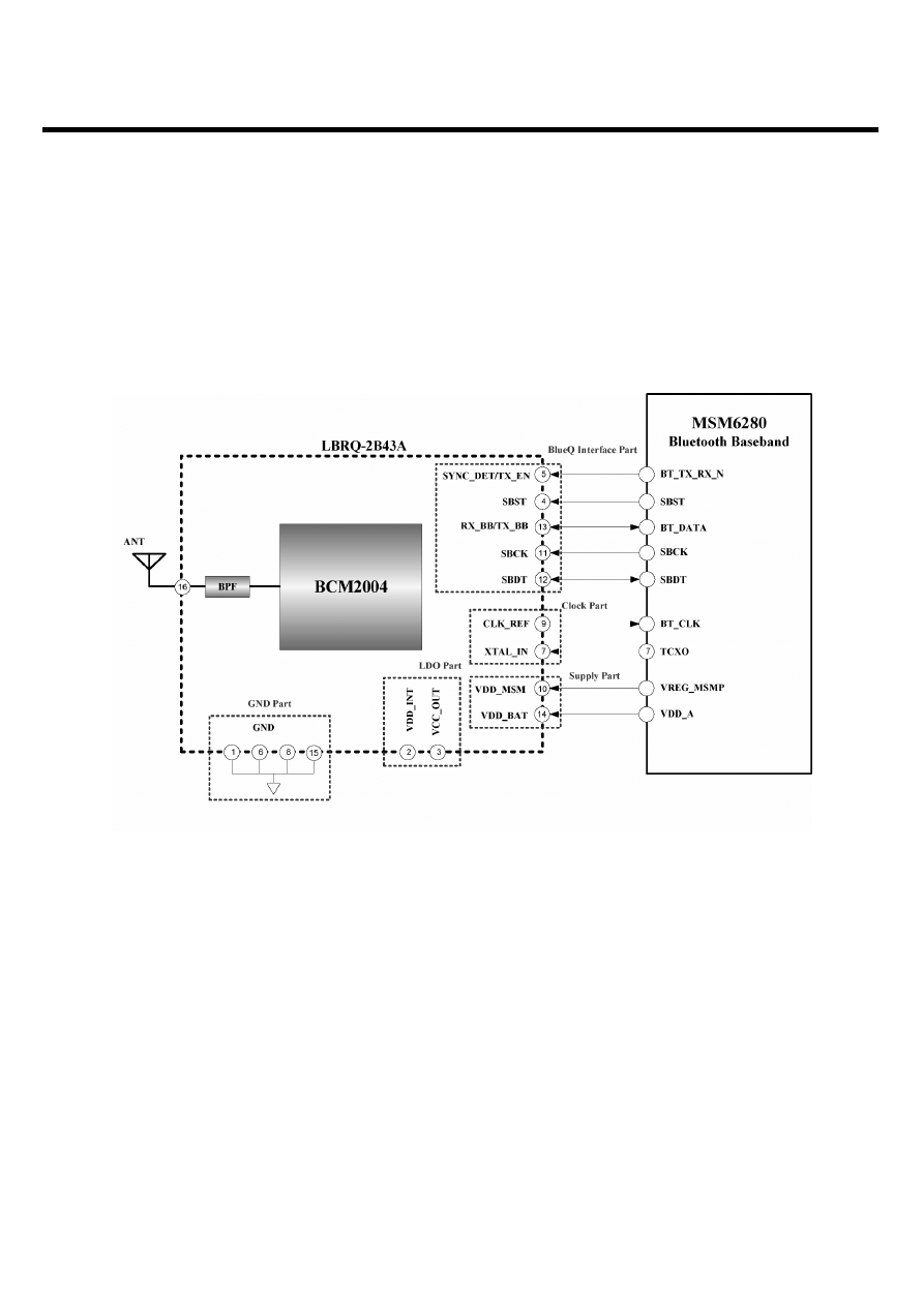
3.5.8 Bluetooth (M800 : LBRQ-2B43A)
The MSM6280 includes BT baseband embedded BT 1.1 compliant baseband core, so the other
bluetooth components are bluetooth RF module and Antenna. Figure1.9 shows the bluetooth system
architecture in the U990.
[Figure 1.9] Bluetooth system architecture
- 36 -
3. TECHNICAL BRIEF
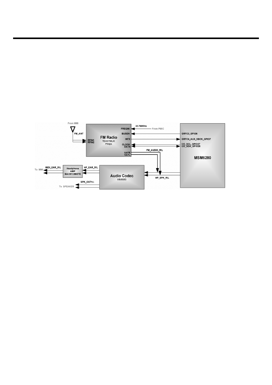
3.5.9 FM Radio (U103 : TEA5766UK)
This FM Module is a single chip, electronically tuned, FM stereo radio with RDS/RBDS demodulator
and decoder for low voltage applications, with fully integrated IF selectivity and demodulation. This
equipment tunes the European, US, and Japanese FM bands.
Figure1.10 shows the FM Radio system architecture in the U990.
LGE Internal Use Only
Copyright © 2007 LG Electronics. Inc. All right reserved.
Only for training and service purposes
[Figure 1.10] FM Radio system architecture in the U990

- 37 -
3. TECHNICAL BRIEF
3.6 Digital Baseband (DBB/MSM6280)
3.6.1 General Description
A. Features (MSM6280)
• Support for multimode operation - HSDPA, tri-band WCDMA (UMTS), quad GSM/GPRS/EDGE
• Support for HSDPA downlink up to 7.2Mbps (initial commercial release will support 3.6Mbps
• HSDPA. Later releases will have support for 7.2 Mbps HSDPA)
• Support for WCDMA (UMTS) uplink data rate up to 384 kbps
• High-performance ARM926EJ-S running at up to 225 MHz (later at 270 MHz for 7.2 Mbps HSDPA)
• ARM Jazelle Java hardware acceleration for faster Java-based games and other applets
• QDSP4000 high-performance DSP cores
• Integrated Bluetooth 1.2 baseband processor for wireless connectivity to peripherals
• Qcamera
TM
with 15 fps QVGA viewfinder resolution, and support for 4 MP camera sensors
• Direct interface to digital camera module with video front end (VFE) image processing
• True 3D graphics for advanced wireless gaming
• SecureMSM v2.0 includes support for Open Mobile Alliance (OMA) DRM v2.0, SIM-lock and IMEI
integrity. Support for Q-fuse.
• Audio on par with portable music players
• Vocoder support (AMR, FR, EFR, HR)
• Advanced 14 x 14 mm, 0.5 mm pitch, 409-pin lead-free CSP packaging technology
• SD/SDIO hardware support
3. BB Technical Description
LGE Internal Use Only
Copyright © 2007 LG Electronics. Inc. All right reserved.
Only for training and service purposes
LGE Internal Use Only
Copyright © 2007 LG Electronics. Inc. All right reserved.
Only for training and service purposes
3. TECHNICAL BRIEF
- 38 -
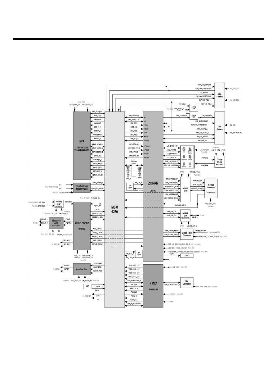
Figure. Simplified Block Diagram of Baseband
LGE Internal Use Only
Copyright © 2007 LG Electronics. Inc. All right reserved.
Only for training and service purposes
3. TECHNICAL BRIEF
- 39 -
Figure. Simplified Block Diagram of RF

- 40 -
3. TECHNICAL BRIEF
LGE Internal Use Only
Copyright © 2007 LG Electronics. Inc. All right reserved.
Only for training and service purposes
3.7 Subsystem(MSM6280)
3.7.1. ARM Microprocessor Subsystem
The MSM6280 device uses an embedded ARM926EJ-S microprocessor. This microprocessor,
through the system software, controls most of the functionality for the MSM, including control of the
external peripherals such as the keypad, LCD, SDRAM, and NAND-Flash devices. Through a
QUALCOMM proprietary serial bus interface (SBI) the ARM926EJ-S configures and controls the
functionality of the RTR6275, RFR6275 and PM6650 devices.
3.7.2 WCDMA R99 features
The MSM6280 device supports release 99 June 2004 of the W-CDMA FDD standard, including the
following features:
■ All modes and data rates for W-CDMA frequency division duplex (FDD), with the following
restrictions:
❏ The downlink supports the following specifications:
- Up to four physical channels, including the broadcast channel (BCH), if present
- Up to three dedicated physical channels (DPCHs)
- Spreading factor (SF) range support from 4 to 256
- The following transmit diversity modes are supported:
Space time transmit diversity (STTD)
Time-switched transmit diversity (TSTD)
Closed-loop feedback transmit diversity (CLTD)
■ The uplink supports the following specifications:
❏ The uplink provides the following UE support:
- One physical channel, eight TrCH, and 16 TrBks starting at any frame boundary
- A maximum data rate of 384 kbps
❏ Full SF range support from 4 to 256
■ SMS (CS and PS)
■ PS data rate - 384 kbps DL / 384 kbps UL
■ CS data rate - 64 kbps DL / 64 kbps UL
■ AMR (all rates)

LGE Internal Use Only
Copyright © 2007 LG Electronics. Inc. All right reserved.
Only for training and service purposes
3. TECHNICAL BRIEF
- 41 -
3.7.3 HSDPA features
The MSM6280 device supports the HSDPA release 5 standard:
■ Supports HS-DSCH (HS-SCCH, HS-PDSCH and HS-DPCCH) in addition to the R99 transport
channels as defined in 3GPP specifications.
■ Supports a maximum of four simultaneous HS-SCCH channels as defined in 3GPP specifications.
■ Supports a maximum of 10 HS-PDSCH channels and supports both QPSK and 16 QAM modulation.
It supports UE category 6 in SW release 2.0 and category 8 in SW release 4.0.
■ Supports CQI, and ACK/NACK on HS-DPCCH channel as defined in 3GPP specifications.
■ Supports all incremental redundancy versions for HARQ, as defined in 3GPP specifications.
■ Can switch between HS-PDSCH and DPCH channel resources, as directed by the network.
■ Can be configured to support any of the two power classes 3 or 4 as defined in 3GPP R5
specifications (25.101).
■ Supports network activation of compressed mode by SF/2 or HLS on the DPCH for conducting inter-
frequency or inter-RAT measurements when the HS-DSCH is active.
■ Supports STTD on both associated DPCH and HS-DSCH simultaneously.
■ Supports CLTD mode 1 on the DPCH when the HS-PDSCH is active.
■ Supports STTD on HS-SCCH when either STTD or CLTD Mode 1 are configured on the associated
DPCH.
■ Supports TFC selection limitation on the UL factoring in the transmissions on the HS-DPCCH as
required in TS 25.133.

LGE Internal Use Only
Copyright © 2007 LG Electronics. Inc. All right reserved.
Only for training and service purposes
3. TECHNICAL BRIEF
- 42 -
3.7.4 GSM features
The following GSM modes and data rates are supported by the MSM6280 device hardware. Support
modes conform to release '99 specifications of the sub-feature.
■ Voice features
❏ FR
❏ EFR
❏ AMR
❏ HR
❏ A5/1, A5/2, and A5/3 ciphering
■ Circuit-switched data features
❏ 9.6k
❏ 14.4k
❏ Fax
❏ Transparent and non-transparent modes for CS data and fax
❏ No sub-rates are supported.
3.7.5 GPRS features
■ Packet switched data (GPRS)
❏ DTM (Simple Class A) operation
❏ Multi-slot class 12 data services
❏ CS schemes: CS1, CS2, CS3, and CS4
❏ GEA1, GEA2, and GEA3 ciphering
■ Maximum of four Rx timeslots per frame
3.7.6 EDGE features
■ EDGE E2 power class for 8 PSK
■ DTM (simple Class A), multi-slot class 12
■ Downlink coding schemes - CS 1-4, MCS 1-9
■ Uplink coding schemes - CS 1-4, MCS 1-9
■ BEP reporting
■ SRB loopback and test mode B
■ 8-bit, 11-bit RACH
■ PBCCH support
■ 1 phase/2 phase access procedures
■ Link adaptation and IR
■ NACC, extended UL TBF.

LGE Internal Use Only
Copyright © 2007 LG Electronics. Inc. All right reserved.
Only for training and service purposes
3. TECHNICAL BRIEF
- 43 -
3.7.7 MSM6280 device audio processing features
■ Integrated wideband stereo CODEC
❏ 16-bit DAC with typical 88 dB dynamic range
❏ Supports sampling rates up to 48 kHz on the speaker path and 16 kHz on the microphone path
■ VR- Voice mail + voice memo
■ Acoustic echo cancellation
■ Audio AGC
■ Audio Codecs: AMR-NB, AAC, AAC Plus, Enhanced AAC Plus, Windows Audio v9, Real Audio 8
(G2)
■ Internal vocoder supporting AMR, FR, EFR, and HR
3.7.8 MSM6280 microprocessor subsystem
■ Industry standard ARM926EJ-S embedded microprocessor subsystem
❏ 16 kB instruction and 16 kB data cache
❏ Instruction set compatible with ARM7TDMI®
❏ ARM version 5TEJ instructions
❏ Higher performance 5 stage pipeline, Harvard cached architecture
❏ Higher internal CPU clock rate with on-chip cache
■ Java hardware acceleration
■ Enhanced memory support
Please note that NOR/PSRAM will not be supported on MSM6280.
❏ 75 MHz and 90 MHz bus clock for SDRAM
❏ 32-bit SDRAM
❏ Dual memory buses separating the high-speed memory subsystem (EBI1) from low-speed
peripherals (EBI2) such as LCD panels
❏ 1.8 V or 2.6 V memory interface support (excluding EBI1)
❏ NAND FLASH memory interface
- 8/16-bit data I/O width NAND flash support
- 1- or 4-bit ECC
- 512-byte/2KB page-size support
- 2 chip selects supported for NAND Flash
❏ Boot from NAND
❏ Low-power SDRAM (LP-SDRAM) interface
■ Internal watchdog and sleep timers

- 44 -
3. TECHNICAL BRIEF
3.7.9 Supported interface features
■ USB On-the-Go core supports both slave and host functionality
■ Three universal asynchronous receiver transmitter (UART) serial ports
■ USIM controller (via UART)
■ Integrated 4-bit secure digital (SD) controller for SD and Mini SD cards
■ Parallel LCD interface
■ General-purpose I/O pins
■ External keypad interface
3.7.10 Supported multimedia features
■ Provide additional general purpose MIPS by using:
❏ Two QDSP4000s
❏ Dedicated hardware accelerators and compression engines
■ Improve Java, BREW, and game performance
❏ Integrated Java and 2D/3D graphics accelerator with Sprite engine
■ Enable various accessories via USB host connectivity.
❏ Integrated USB host controller functionality
■ Enable compelling visual and audio applications.
Qcamera
TM
■ High-quality digital camera processing, supporting CCD or CMOS image sensors up to 4-megapixel
with 15 fps capture rate
■ 15 fps QVGA viewfinder
Qtv
TM
■ Audio and video decoder that supports VOD, MOD and Broadcast multimedia services.
■ Audio Codecs supported: AMR-NB, AAC, AAC Plus, Enhanced AAC Plus, Windows® Audio v9,
RealAudio® v8
■ Integrated stereo wideband Codec for music/digital clips
■ CMX
■ Video Codecs supported: MPEG-4, H.263, H.264, Windows Media® v9 and RealNetworks® v10
Video telephony services: Qvideophone
TM
■ A two-way mobile video conferencing solution that delivers 15 fps @ QCIF
■ Video Codecs supported: MPEG-4 and H.263
■ Audio Codecs supported: AMR-NB.
LGE Internal Use Only
Copyright © 2007 LG Electronics. Inc. All right reserved.
Only for training and service purposes

- 45 -
3. TECHNICAL BRIEF
Qcamcorder
TM
■ Real time mobile video encoder
■ Video Codecs supported: MPEG-4, H.263.H.264
■ Audio Codecs supported: AMR-NB, AAC
■ Recording performance: 15 fps @ QVGA, 384 kbps
gpsOne
TM
■ Integrated gpsOne processing
■ Standalone gpsOne mode in which the handset acts as a GPS receiver
CMX
TM
(MIDI and still image, animation, text, LED/vibrate support)
■ 72 simultaneous polyphonic tones
■ 44 kHz sampling rate
■ 512 kB wave table
■ Support of universal file formats
❏ Standard MIDI Format (SMF)
❏ SP-MIDI
❏ SMAF Audio playback (MA-2, MA-3, MA-5)
❏ XMF/OLS
❏ MFil (requires Docomo license)
■ PNG decoder
■ Pitch bend range support
■ LED/vibrate support
■ Scalable Vector Graphics (SVG- Tiny 1.1 + SVG Tiny 1.2)
■ MLZ decoder
■ Integrated PNG/SAF A.T.
LGE Internal Use Only
Copyright © 2007 LG Electronics. Inc. All right reserved.
Only for training and service purposes
- 46 -
3. TECHNICAL BRIEF
3.7.11 Serial Bus Interface(SBI)
The MSM6280 device’s SSBI is designed specifically to be a quick, low pin count control protocol for
QUALCOMM’s RTR6275, RFR6275 and PM6650 ASICs. Using the SSBI, the RTR6275, RFR6275,
and PM6650 devices can be configured for different operating modes and for minimum power
consumption, extending battery life in Standby mode. The SSBI also controls DC baseband offset
errors.
3.7.12 Wideband CODEC
The MSM6280 device integrates a wideband voice/audio CODEC into the mobile station modem
(MSM). The CODEC supports two differential microphone inputs, one differential earphone output, one
single-ended earphone output, and a differential analog auxiliary interface. The CODEC integrates the
microphone and earphone amplifiers into the MSM6280 device, reducing the external component
count to just a few passive components. The microphone (Tx) audio path consists of a two-stage
amplifier with the gain of the second stage set interally. The Rx/Tx paths are designed to meet the
ITU-G.712 requirements for digital transmission systems.
LGE Internal Use Only
Copyright © 2007 LG Electronics. Inc. All right reserved.
Only for training and service purposes

- 47 -
3. TECHNICAL BRIEF
3.7.13 Vocoder Subsystem
The MSM6280 device’s QDSP4000 supports AMR,FR,EFR and HR. In addition, the QDSP4000 has
modules to support the following audio functions: DTMF tone generation, DTMF tone detection, Tx/Rx
volume controls, Tx/Rx automatic gain control (AGC), Rx Automatic Volume Control (AVC), EarSeal
Echo Canceller (ESEC), Acoustic Echo Canceller (AEC), Noise Suppression (NS), and programmable,
13-tap, Type-I, FIR, Tx/Rx compensation filters. The MSM6280 device’s integrated ARM9TDMI
processor downloads the firmware into the QDSP4000 and configures QDSP4000 to support the
desired functionality.
3.7.14 ARM Microprocessor subsystem
The MSM6280 device uses an embedded ARM926EJ-S microprocessor. This microprocessor,
through the system software, controls most of the functionality for the MSM device, including control of
the external peripherals such as the keypad, LCD, RAM, ROM, and EEPROM devices.
Through a generic single serial bus interface (SSBI) the ARM926EJ-S configures and controls the
functionality of the RFR6275, RTR6275, and PM6650 devices.
3.7.15 Mode Select and JTAG Interfaces
The mode pins to the MSM6280 device determine the overall operating mode of the ASIC. The options
under the control of the mode inputs are Native mode, which is the normal subscriber unit operation,
ETM mode, which enables the built-in trace mode, and test mode for factory testing. The MSM6280
device meets the intent of the ANSI/IEEE 1149.1A-1993 feature list. The JTAG interface can be used
to test digital interconnects between devices within the mobile station during manufacture.
3.7.16 General-Purpose Input/Output Interface
The MSM6280 device has general-purpose bidirectional input/output pins. Some of the GPIO pins
have alternate functions supported on them. The alternate functions include USB interface, additional
RAM, ROM, general-purpose chip selects, parallel LCD interface, and a UART interface. The function
of these pins is documented in the various software releases.
3.7.17 UART
The MSM6280 device employs three UARTs. UART1 has dedicated pins while UART2 and UART3
share multiplexed pins.
■ UART1 for data
■ UART2 (can be used for USIM interface)
■ UART3 for data
3.7.18 USB
The MSM6280 device integrates a universal serial bus (USB) controller that supports both
unidirectional and bidirectional transceiver interfaces. The USB controller acts as a USB peripheral
communicating with the USB host.
LGE Internal Use Only
Copyright © 2007 LG Electronics. Inc. All right reserved.
Only for training and service purposes

- 48 -
3. TECHNICAL BRIEF
3.8 Power Block
3.8.1 General
MSM6280, included RF, is fully covered by PM6650(Qualcomm PMIC). PM6650 cover the power of
MSM6280, MSM memory, RF block, Bluetooth, USIM and TCXO. Major power components are :
PM6650 : Phone power supply
AAT3169 : LCD Backlight/Flash charge pump
3.8.2 PM6650
The PM6650 device (Figure 1-1) integrates all wireless handset power management. The power
management portion accepts power from all the most common sources - battery, external charger,
adapter, coin cell back-up - and generates all the regulated voltages needed to power the appropriate
handset electronics. It monitors and controls the power sources, detecting which sources are applied,
verifying that they are within acceptable operational limits, and coordinates battery and coin cell
recharging while maintaining the handset electronics supply voltages. Eight programmable output
voltages are generated using low dropout voltage regulators, all derived from a common trimmed
voltage reference.
A dedicated controller manages the TCXO warm-up and signal buffering, and key parameters (under-
voltage lockout and crystal oscillator signal presence) are monitored to protect against detrimental
conditions.
MSM device controls and statuses the PM6650 IC using Single Serial Bus Interface (SSBI)
supplemented by an Interrupt Manager for time-critical information. Another dedicated IC Interface
circuit monitors multiple trigger events and controls the power-on sequence.
LGE Internal Use Only
Copyright © 2007 LG Electronics. Inc. All right reserved.
Only for training and service purposes
- 49 -
3. TECHNICAL BRIEF
LGE Internal Use Only
Copyright © 2007 LG Electronics. Inc. All right reserved.
Only for training and service purposes
Figure 1-1. PM6650 Functional Block Diagram
- 50 -
3. TECHNICAL BRIEF
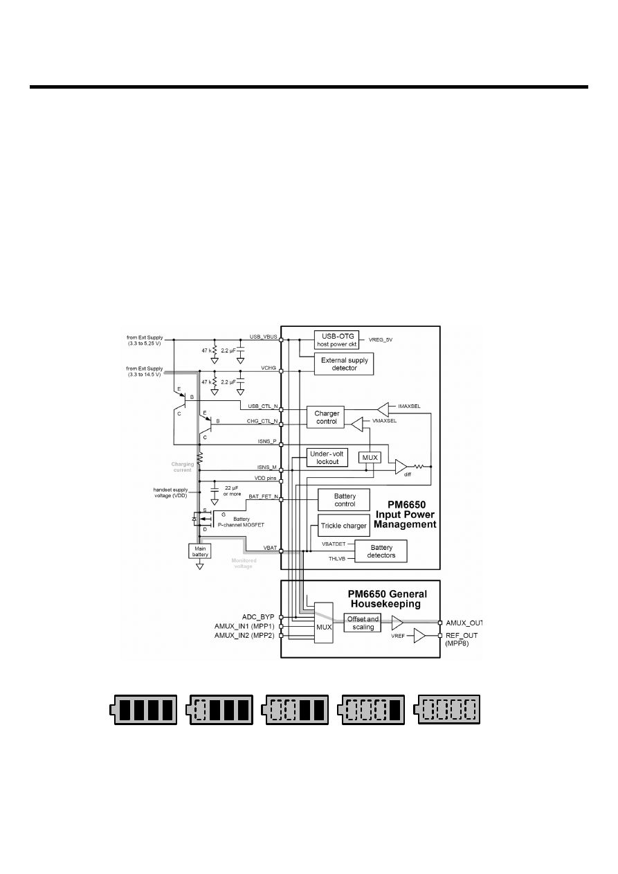
3.8.3 Charging control
A programmable charging block in PM6650 is used for battery charging. It is possible to set limits for
the charging current. The external supply typically connects directly to pin (VCHG). The voltage on this
pin (VCHG) is monitored by detection circuitry to ascertain whether a valid external supply is applied or
not. For additional accuracy or to capture variations over time, this voltage is routed internally to the
housekeeping ADC via the analog multiplexer. PM6650 circuits monitor voltages at VCHARGER and
ICHARGE pins to determine which supply should be used and when to switch between the two
supplies. These pins are connected to the Source (or emitter) and Drain (or collector) contacts of the
pass transistor respectively.
LGE Internal Use Only
Copyright © 2007 LG Electronics. Inc. All right reserved.
Only for training and service purposes
4.2V~3.81V
100~70 (%)
3.80V~3.71V
69~45 (%)
3.70V~3.62V
44~20 (%)
3.61V~3.50V
19~3 (%)
3.49V~3.28V
2~0 (%)
KU990 Battery Bar Display(Stand By Condition)
- 51 -
3. TECHNICAL BRIEF
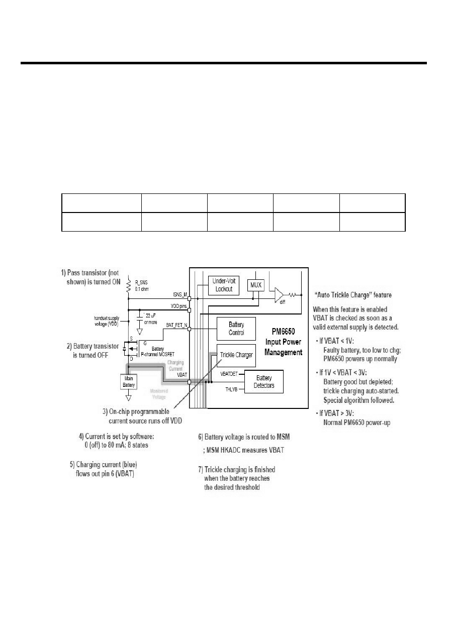
Trickle Charging
Trickle Charging of the main battery, enabled through SBI control and powered from VDD, is provided
by the PM6650 IC, The trickle charger is on-chip programmable current source that supplies current
from VDD to pin (VBAT). Trickle charging can be used for lithium-ion and nickel-based batteries, with
its performance specified below (3.2V). The charging current is set to 80mA.
LGE Internal Use Only
Copyright © 2007 LG Electronics. Inc. All right reserved.
Only for training and service purposes
Parameter
Min
Typ
Max
Unit
Trickle Current
60
80
100
mA

- 52 -
3. TECHNICAL BRIEF
Constant Current Charging
The PM6650 IC supports constant current charging of the main battery by controlling the charger pass
transistor and the battery transistor. The constant current charging continues until the battery reaches
its target voltage, 4.2V.
Constant Voltage Charging
Constant voltage charging begins when the battery voltage reaches a target voltage, 4.2V. The end of
constant voltage charging is commonly detected 10% of the full charging current.
• Charging Method : CC & CV (Constant Current & Constant Voltage)
• Maximum Charging Voltage : 4.2V
• Maximum Charging Current : 600mA
• Nominal Battery Capacity : 1000mAh
• Charger Voltage : 5.1V
• Charging time : Max 3h (Except time trickle charging)
• Full charge indication current (icon stop current) : 100mA
• Low battery POP UP : Idle - 3.49V, Dedicated(GSM/WCDMA) - 3.49V
• Low battery alarm interval : Idle - 3 min, Dedicated - 1min
• Cut-off voltage : 3.20V(idle), 3.1V(call)
LGE Internal Use Only
Copyright © 2007 LG Electronics. Inc. All right reserved.
Only for training and service purposes
- 53 -
3. TECHNICAL BRIEF
LGE Internal Use Only
Copyright © 2007 LG Electronics. Inc. All right reserved.
Only for training and service purposes
3.9 External memory interface
The MSM6280 device was designed to provide two distinct memory interfaces. EBI1 was targeted for
supporting high speed synchronous memory devices. EBI2 was targeted towards supporting slower
asynchronous devices such as LCD, NAND flash, SRAM, etc. In addition, MSM6280 provide SD bus
interface. KU990 supports 512MByte free user memory using SD interface.
• EBI1 Features
- 16 bit static and dynamic memory interface
- 32 bit dynamic memory interface
- 24 bits of address for static memory devices which can support up to 32MBytes on each chip select
- Synchronous burst memories supported (burst NOR, burst PSRAM)
- Synchronous DRAM memories supported
- Byte addressable memory supporting 8 bit, 16 bit and 32 bit accesses
- Pseudo SRAM (PSRAM) memory support
• EBI2 Features
- Support for asynchronous FLASH and SRAM(16bit & 8bit).
- Interface support for byte addressable 16bit devices (UB_N & LB_N signals).
- 2Mbytes of memory per chip select.
- Support for 8 bit/16bit wide NAND flash.
- Support for parallel LCD interfaces, port mapped of memory mapped(18 or 16 bit).
• 2Gb NAND(16bit, Large Block ) flash memory + 1Gb SDRAM (32bit)
• 1-CS(Chip Select) are used.
• The SD bus allows the dynamic configuration of the number of data line from 1 to 4 Bidirectional data
signal. After power up by default, the Device will use only DAT0. After initialization, host can change
the bus width.
Interface Spec
Device
Part Name
Maker
Read Access Time
Write Access Time
NAND
TYA000BC00DOGG
Toshiba
50 ns
30 ns
SDRAM
TYA000BC00DOGG
Toshiba
15 ns
15 ns
Table#1. External memory interface
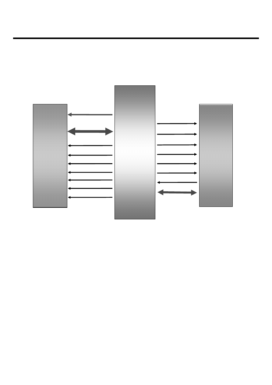
- 54 -
3. TECHNICAL BRIEF
LGE Internal Use Only
Copyright © 2007 LG Electronics. Inc. All right reserved.
Only for training and service purposes
Figure. Simplified Block Diagram of Memory Interface
MSM6280
SDRAM
1Gbit
(512M x 2)
NAND
2Gb
(256MB)
DATA[31:0]
ADDRESS[14:0]
WE*
CS*
CAS*
RAS*
CLK_EN
CLK
DQM[3:0]
NAND_CS*
NAND_RE*
NAND_WE*
NAND_CLE
NAND_WP*
NAND_ALE
NAND_READY
DATA[15:0]
EBI1
EBI2
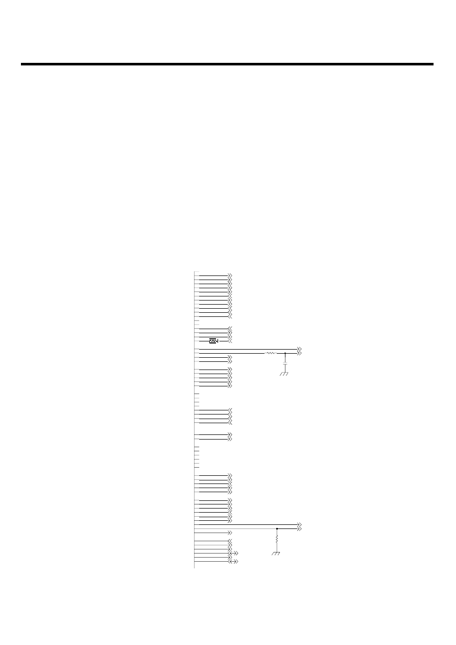
- 55 -
3. TECHNICAL BRIEF
LGE Internal Use Only
Copyright © 2007 LG Electronics. Inc. All right reserved.
Only for training and service purposes
3.10 H/W Sub System
3.10.1 RF Interface
A. RTR6275(WCDMA_Tx, GSM_Tx/Rx)
MSM6280 controls RF part(RTR6275) using these signals.
• SBST : SSBI I/F signals for control Sub-chipset
• PA_ON1 : Power AMP on RF part
• RX0_I/Q_M/P,TX_I/Q_M/P : I/Q for T/Rx of RF
• TX_AGC_ADJ : control the gain of the Tx signal prior to the power amplifier
• DAC_REF : Reference input to the MSM Tx data DACs
(WCMDA 2100 PAM Enable)
R213
NA
33nF
C223
R211
2K
0
R215
AA1
XMEM1_CS_N1_GPIO76
XMEM1_CS_N3_SDRAM1_CS_N1_GPIO77
Y6
XMEM2_CS_N2_GPIO35
W15
AA15
XMEM2_CS_N3_GPIO36
H6
UART2_DP_RX_DATA_GPIO89
L25
UART3_RFR_N_GPIO87
USB_RX_DATA_GPIO29
N19
B6
SYNTH2_GPIO65
TCK
D16
TCXO_EN_GPIO94
F19
TDI
D15
TDO
A17
TMS
F15
TRK_LO_ADJ
L13
H15
TRST_N
H13
TX_AGC_ADJ
TX_ON_GRFC10
H12
F18
SYNTH0_GP_PDM0_GPIO92
RTCK
H16
SBDT1_GPIO1
SBST1_GPIO93
H18
PA_ON0
F17
PA_ON1_GPIO2
H11
AA25
Q_IM_CH0
Q_IM_CH1
W23
Y25
Q_IP_CH0
Q_IP_CH1
V23
B12
Q_OUT
A12
Q_OUT_N
AE13
LCD_EN_GPIO37
A22
AB25
I_IM_CH0
V25
I_IM_CH1
AC25
I_IP_CH0
I_IP_CH1
W25
I_OUT
B13
I_OUT_N
A13
D17
GP_PDM2_PA_RAN_GE1
B8
GRFC0_GPIO3
A8
GRFC1_AUX_SBDT_GPIO4
D9
GRFC2_GPIO5
GRFC3_GPIO6
F10
GRFC4_AUX_SBCK_GPIO7
H10
D11
GRFC5_AUX_SBST_GPIO8
GRFC7_GPIO10
T23
B4
GRFC8_GPIO11
D5
GRFC9_GPIO12
GRFX6_GPIO9
T19
F8
GPIO66
GP_PDM1_PA_RAN_GE0
H17
F12
DAC_REF
A6
GPIO28
H9
GPIO43
R19
BT_DATA_GPIO20
E26
BT_SBCK_GPIO23
BT_SBDT_GPIO22
E25
F23
BT_SBST_GPIO24
BT_TX_RX_N_GPIO21
H21
CAMCLK_PO_GP_MN_GPIO13
J21
AUX_PCM_CLK_GRFC14_GPIO80
K19
N21
AUX_PCM_DIN_GRFC13_GPIO14
G4
AUX_PCM_DOUT_GRFC12_GPIO103
AUX_PCM_SYNC_GRFC11_GPIO102
J8
G23
BT_CLK_GPIO25
MMP_INT_N
RMT_INT
CAM_MCLK
LCD_RESET_N
VGA_CAM_RESET_N
CAM_SELECT_N
MICROSD_DETECT
VGA_CAM_PWDN
BT_DATA
BT_SBDT
BT_SBCK
BT_SBST
BT_TX_RX_N
BT_CLK
MMP_HPCM_FSYNC
LCD_LDO_EN
MMP_HPCM_DI
MMP_HPCM_CLK
MMP_HPCM_DO
RX_IM
RX_IP
RX_QM
RX_QP
DAC_REF
PA_ON
TCXO_EN
TRK_LO_ADJ
TX_AGC_ADJ
LIN_INVERTER
HOOK_SENSE_N
LCD_IF_MODE
CAM_MODE1_N
CAM_MODE3_N
HP_AMP_EN
TX_QM
TX_IM
GSM_PA_EN
TX_QP
TX_IP
ANT_SEL2
GSM_PA_BAND
FM_INTX
TX_ON
PA_R1
ANT_SEL0
ANT_SEL1
FM_BUSEN
USB_SELECT_N
LIN_PWM_MAG
LIN_MOTOR_EN
Figure. Schematic of RF Interface of MSM6280

- 56 -
3. TECHNICAL BRIEF
LGE Internal Use Only
Copyright © 2007 LG Electronics. Inc. All right reserved.
Only for training and service purposes
B. the others
• TRK_LO_ADJ : TCXO(19.2M) Control
• PA_ON : WCDMA(2100) TX Power Amp Enable
• ANT_SEL[0-2] : Ant Switch Module Mode Selection(WCDMA,GSM Tx/Rx,DCS-PCS Tx/Rx)
• GSM_PA_BAND : GSM/DCS-PCS Band Selection of Power Amp
• GSM_PA_RAMP : Power Amp Gain Control of APC_IC
• GSM_PA_EN : Power Amp Gain Control Enable of APC_IC
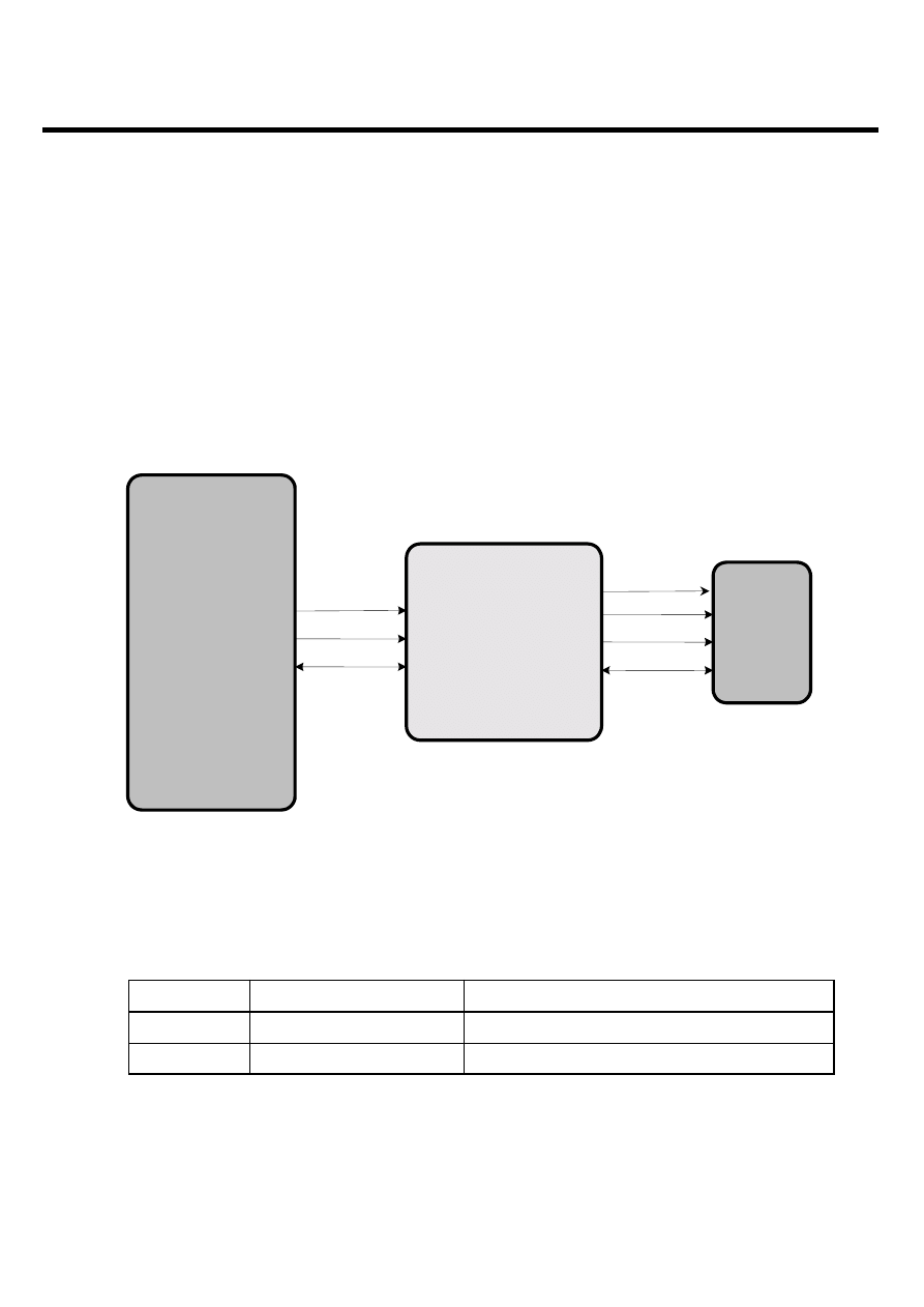
- 57 -
3. TECHNICAL BRIEF
LGE Internal Use Only
Copyright © 2007 LG Electronics. Inc. All right reserved.
Only for training and service purposes
3.10.2 MSM Sub System
3.10.2.1. USIM Interface
SIM interface scheme is shown in Figure.
And, there control signals are followed
• USIM_CLK : USIM Clock
• USIM_Reset : USIM Reset
• USIM_Data : USIM Data T/Rx
3.10.2.2 UART Interface
UART signals are connected to MSM GPIO through IO connector with 115200 bps speed.
MSM6280
PM6650
USIM
USIM CLK
USIM Reset
USIM Data
USIM Data
USIM Reset
USIM CLK
VREG_UIM 2.85V
Figure. SIM Interface
GPIO_Map
Name
Note
GPIO_96
UART_RXD
Data_Rx
GPIO_95
UART_TXD
Data_Tx
Table. UART Interface
- 58 -
3. TECHNICAL BRIEF
LGE Internal Use Only
Copyright © 2007 LG Electronics. Inc. All right reserved.
Only for training and service purposes
3.10.2.3 USB
The MSM6280 device contains a Universal Serial Bus (USB) interface to provide an efficient
interconnect between the mobile phone and a personal computer (PC). The USB interface of the
MSM6280 was designed to comply with the definition of a peripheral as specified in USB Specification,
Revision 1.1. Therefore, by definition, the USB interface is also compliant as a peripheral with the USB
Specification, Revision 2.0. The USB Specification Revision 1.1 defines two speeds of operation,
namely low-speed (1.5 Mbps) and full-speed (12 Mbps), both of which are supported by the
MSM6280.
Name
Note
USB_DAT
Data to/from MSM
USB_SE0
Data to/from MSM
USB_OE_N
Out-Put Enable of Transceiver
USB_VBUS
USB_Power From Host(PC)
USB_D+
USB Data+ to Host
USB_D
USB Data- to Host
Table. USB Signal Interface
Figure. Schematic of USB block(MSM6280 Side & PM6650 Side)
USB_DAT_VP
N26
N25
USB_OE_TP_N
USB_SE0_VM
N23
M16
MMC_CLK_SDCC
MMC_CMD_GPIO
H14
L14
MMC_DATA_SDC
GPIO40
D6
D7
GPIO42
PM_INT_N
PS_HOLD
USB_SE0
USB_DAT
USB_OE_N
ICROSD_CMD
OSD_DATA[0]
MICROSD_CLK
USB_CTL_N
USB_VBUS
16
USB_DAT
17
USB_D_P
18
19
USB_SE0
USB_D_M
20
GP1_DRV_N(M
21
4.7u
C540
47K
R514
USB_VBUS
USB_DAT
MSM_USB_D+
USB_SE0
MSM_USB_D-
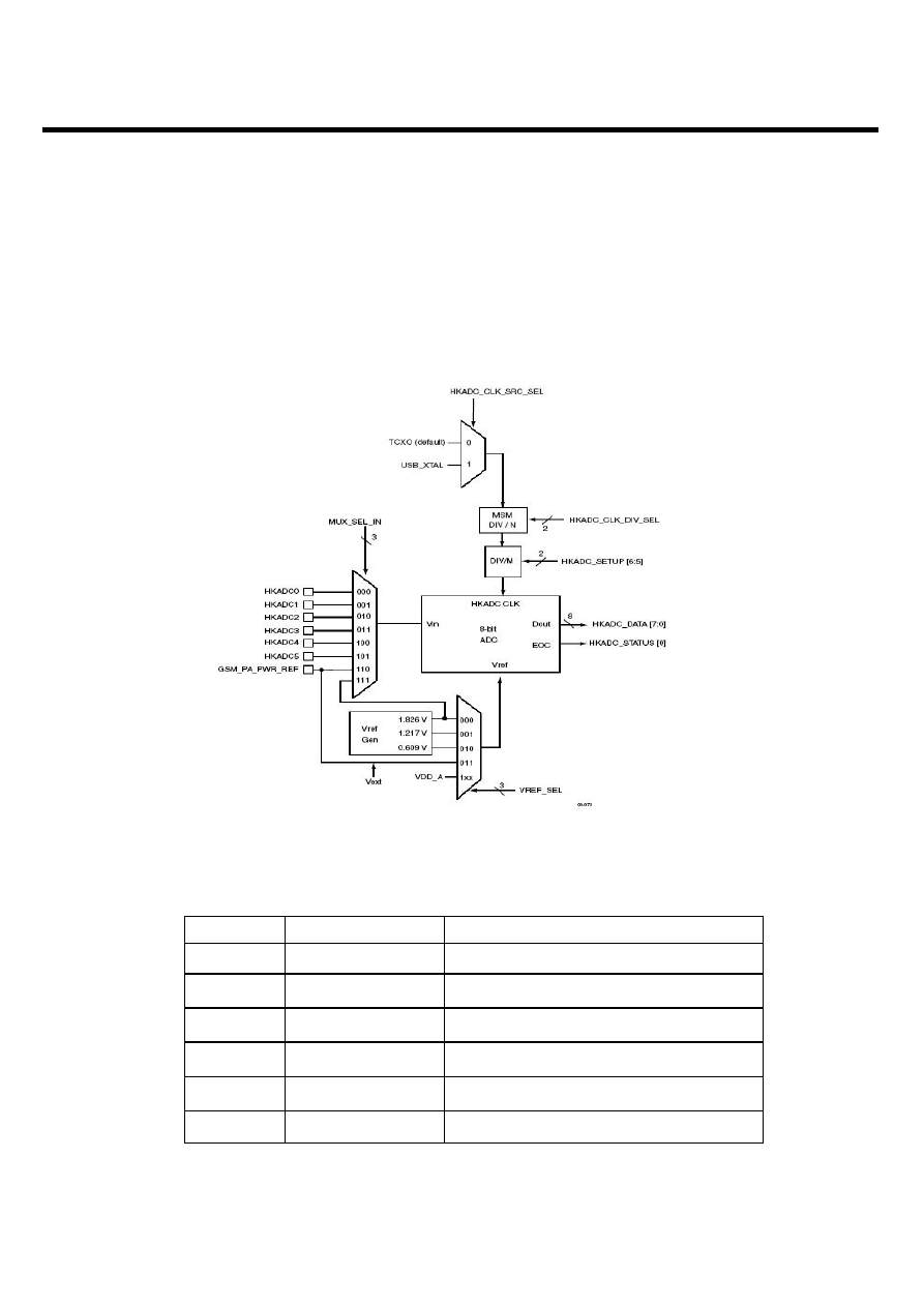
- 59 -
3. TECHNICAL BRIEF
LGE Internal Use Only
Copyright © 2007 LG Electronics. Inc. All right reserved.
Only for training and service purposes
3.10.3 HKADC(House Keeping ADC)
The MSM6280 device has an on-chip 8-bit analog-to-digital converter (HKADC) which is tended to
digitize DC signals corresponding to analog parameters such as battery voltage, temperature, and RF
power levels. The MSM6280 device has six analog input pins which are multiplexed to the input of the
internal HKADC.
Figure. MSM6280HKADC Block diagram
Table. HKADC channel table
PCB Version Check
PCB_Rev_ADC
HKADC4
ADC Reference voltage
REF_ADC
HKADC2
Ear jack Detection for TTY
TTY_ADC_DET
HKADC3
Battery Temperature Check
Battery voltage level
RF PAM Temperature Check
Note
Battery_THERM
VBATT_SENSE
AMUX_OUT
Signal
HKADC5
HKADC1
HKADC0
Channel
3.10.4 Key Pad
There are 5 key buttons. Shows the Key Matrix & Keypad circuit.
‘END’ Key is connected to PMIC(PM6650).
- 60 -
3. TECHNICAL BRIEF
LGE Internal Use Only
Copyright © 2007 LG Electronics. Inc. All right reserved.
Only for training and service purposes
Table. Key Matrix Mapping Table
Figure. Main Keypad Circuit
CLR
SEND
ROW(2)
AF
ROW(1)
Capture
Lock
ROW(0)
COL(1)
COL(0)
CLR
SEND
R701
51K
701
700
VA702
EVLC14S02050
VA701
EVLC14S02050
EVLC14S02050
VA703
KEY_ROW[2]
VREG_MSMP_2.7V
KEY_COL[0]
KEY_COL[1]
- 61 -
3. TECHNICAL BRIEF
LGE Internal Use Only
Copyright © 2007 LG Electronics. Inc. All right reserved.
Only for training and service purposes
Figure. Side Keypad Circuit
LOCK KEY
FOCUS
CAMERA
SW1100
KEY_ROW[1]
KEY_ROW[0]
KEY_COL[0]
KEY_COL[1]
1100
Figure. END Keypad Circuit
END
ON_SW KEY
EVL14K02200
VA700
END
PM_ON_SW_N
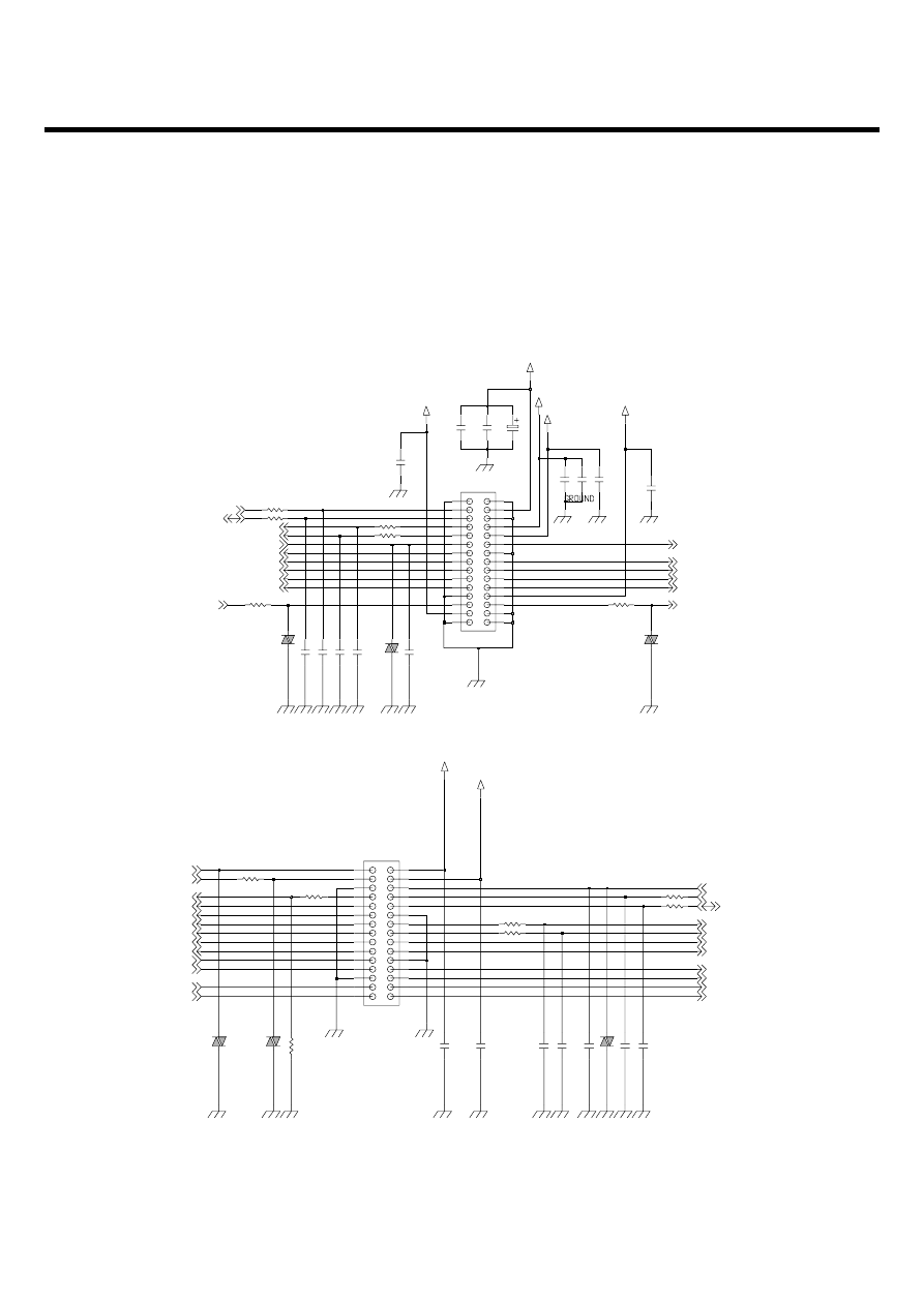
3.10.5 Camera Interface
U990 Installed a 5M Pixel and 0.3Mega Camera.
Below figure shows the camera board to board connector and camera I/F signal.
- 62 -
3. TECHNICAL BRIEF
LGE Internal Use Only
Copyright © 2007 LG Electronics. Inc. All right reserved.
Only for training and service purposes
Figure. Camera PCB Board to Board Connector
GB042-30S-H10-E3000
1u
CAM_VDD_SA_2.7V
CAM_VDD_IO_2.7V
C608
C605
0.1u
10p
C610
30
17
18
19
20
21
22
23
24
14
15
2
3
4
5
6
7
8
9
16
25
26
27
28
29
CN600
1
10
11
12
13
0.1u
C612
C606
10p
R601 10
R607
33
0.1u
C607
10p
C611
CAM_VDD_AF_2.7V
CAM_VDD_CORE_1.2V
VA601
ICVL0518100Y500FR
VA602
C614
EVLC18S02015
0.1u
C601
0.1u
ICVL0518100Y500FR
VA600
10u
C600
R604
10
CAM_VDD_SD_1.8V
10
R603
10p
C613
C609
0.1u
R608
10
C602
1u
R602 10
STROBE_TRIGGER
MMP_CAM_PCLK
5M_CAM_DATA[0]
5M_CAM_DATA[1]
5M_CAM_DATA[2]
5M_CAM_DATA[3]
5M_CAM_DATA[4]
5M_CAM_DATA[5]
5M_CAM_DATA[6]
5M_CAM_DATA[7]
MMP_CAM_RESET_N
MMP_CAM_INT
MMP_CAM_HSYNC
MMP_CAM_VSYNC
MMP_I2C_SDA
MMP_I2C_SCL
5M_CAM_MCLK
10
R719
VGA_VDD_2.7V
R725
10
10
R724
16
25
26
27
28
29
30
17
18
19
20
21
22
23
24
1
10
11
12
13
14
15
2
3
4
5
6
7
8
9
CN701
C711
0.1u
10p
C713
R718
10
EVLC18S02015
VA715
R729
NA
resistor
10p
C715
10
R717
VA714
ICVL0518100Y500FR
10
R720
C712
10p
EVLC18S02015
VA713
C709
0.1u
VGA_VDD_1.8V
C714
10p
0.1u
C710
VGA_CAM_DATA[2]
VGA_CAM_DATA[3]
VGA_CAM_DATA[4]
VGA_CAM_DATA[7]
I2C_SDA
I2C_SCL
MMP_CAM_VSYNC
MMP_CAM_HSYNC
VGA_CAM_RESET_N
RCV+
RCV-
MOTOR+
MOTOR-
x+
x-
Y+
Y-
VGA_CAM_DATA[6]
VGA_CAM_PWDN
VGA_CAM_DATA[5]
VGA_CAM_MCLK
MMP_CAM_PCLK
VGA_CAM_DATA[0]
VGA_CAM_DATA[1]
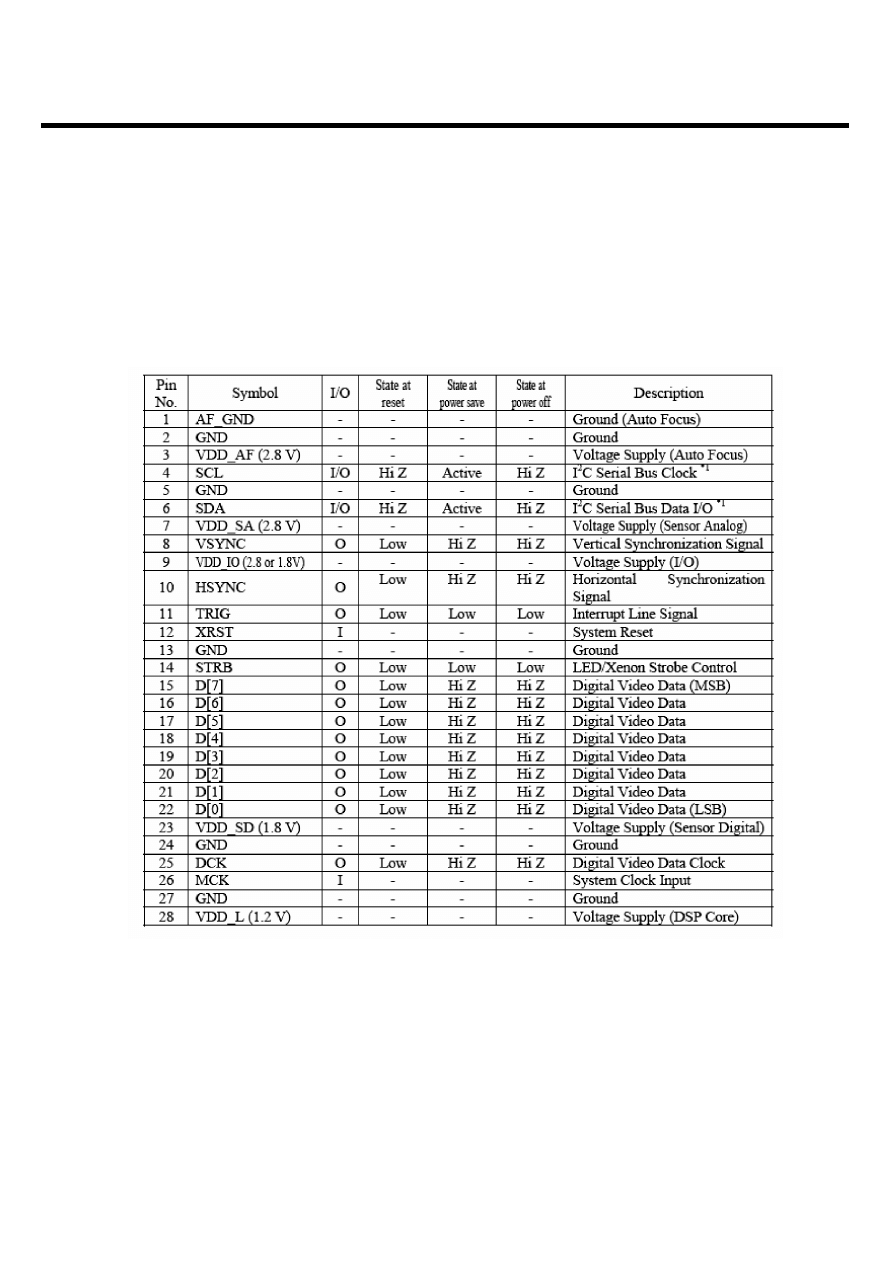
- 63 -
3. TECHNICAL BRIEF
LGE Internal Use Only
Copyright © 2007 LG Electronics. Inc. All right reserved.
Only for training and service purposes
The MEGA Camera module is connected to Main PCB with 30pin Board to Board connector Its
interface is dedicated camera interface port in Multimedia chip. The camera port supply 13MHz master
clock to camera module, vertical sync signal, horizontal sync signal, reset signal and 8bits data from
camera module. The camera module is controlled by I2C port from Multimedia chip.
[ Pin Description ]
Table. Interface between MEGA Camera Module and MAIN PCB (in camera module)
The VGA Camera module is connected to FPCB with 20pin Board to Board connector (AXK720147G).
Its interface is dedicated camera interface port in MSM6280. The camera port supply 13.MHz master
clock to camera module and receive 13MHz pixel clock (15fps), vertical sync signal, horizontal sync
signal, reset signal and 8bits data from camera module. The camera module is controlled by I2C port
from MSM6280.
[ Pin Description ]
- 64 -
3. TECHNICAL BRIEF
LGE Internal Use Only
Copyright © 2007 LG Electronics. Inc. All right reserved.
Only for training and service purposes
Table. Interface between VGA Camera Module and FPCB (in camera module)
Camera I/O Power
I
VREG_CAM_2.8V
20
Camera I/O Power
I
VREG_MSMP_2.8V
19
Camera reset signal
I
CAM_RESET_N
18
I2C Clock
I
I2C_SCL
17
GND
GND
GND
15
I2C Clock
I
I2C_SCD
16
GND
GND
GND
3
Clock for Camera Data Out(13M)
O
CAM_PCLK
4
Data
O
CAM_DATA(0)
5
Data
O
CAM_DATA(1)
6
Data
O
CAM_DATA(2)
7
Data
O
CAM_DATA(3)
8
Data
O
CAM_DATA(4)
9
Data
O
CAM_DATA(5)
10
Horizontal Sync
O
CAM_HSYNC
14
Vertical Synch
O
CAM_VSYNC
13
Data
O
CAM_DATA(7)
12
Data
O
CAM_DATA(6)
11
Master Clock(24M)
I
CAM_MCLK
2
Camera power down
i
CAM_PWDN
1
Note
Port
Name
No
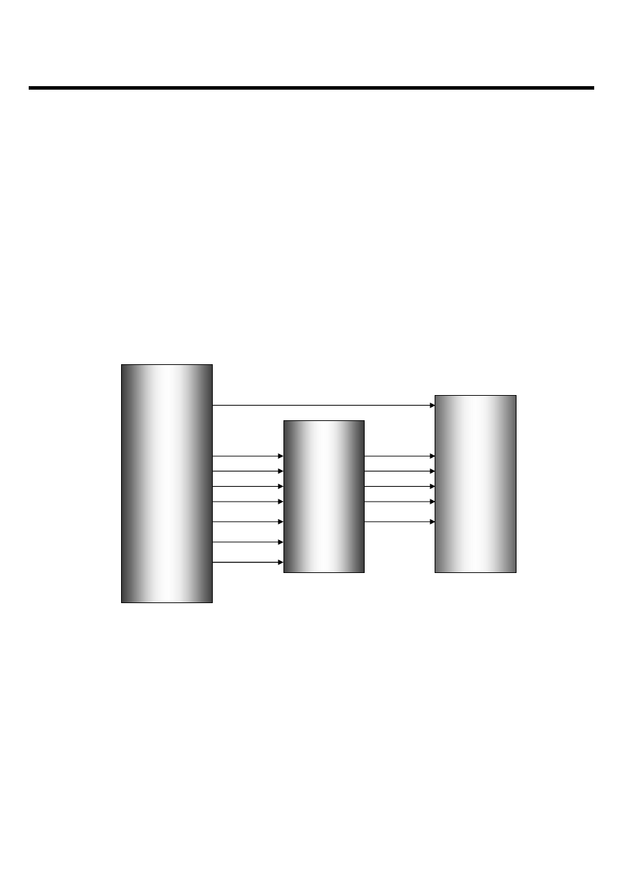
- 65 -
3. TECHNICAL BRIEF
LGE Internal Use Only
Copyright © 2007 LG Electronics. Inc. All right reserved.
Only for training and service purposes
3.10.6 LCD Module (LS030B3UX01 : SHARP)
- The IM220DBN2A model is a Color TFT Main supplied by SHARP.
This LCD Module has a 3.0 inch diagonally measured active display area with 240(RGB)X400
resolution. each pixel is divided into Red, Green and Blue sub-pixels and dots which are arranged in
vertical stripes.
* Features
- Display mode(Main LCD) : Normally Black, Transmissive VA mode 265K colors
- LCD Driver IC: LS030B3UX01(Magnachip)
- Driving Method : A-Si TFT Active Matrix
- 16 bit CPU interface Parallel
Figure. LCD Module Block Diagram
EBI2_OE_N
EBI2_WE_N
EBI2_ADDR[11]
EBI2_DATA[0:15]
MMP_CS_N
LCD_RESET_N
LCD_MAKER_ID
LCD_IF_MODE
MMP_LCD_CS_N
MMP_LCD_RD_N
MMP_LCD_WE_N
MMP_LCD_ADS
MMP_LCD_DATA[0:15]
MSM6280
Multimedia
Chip
LCD 3.0î
TFT(WQVGA)
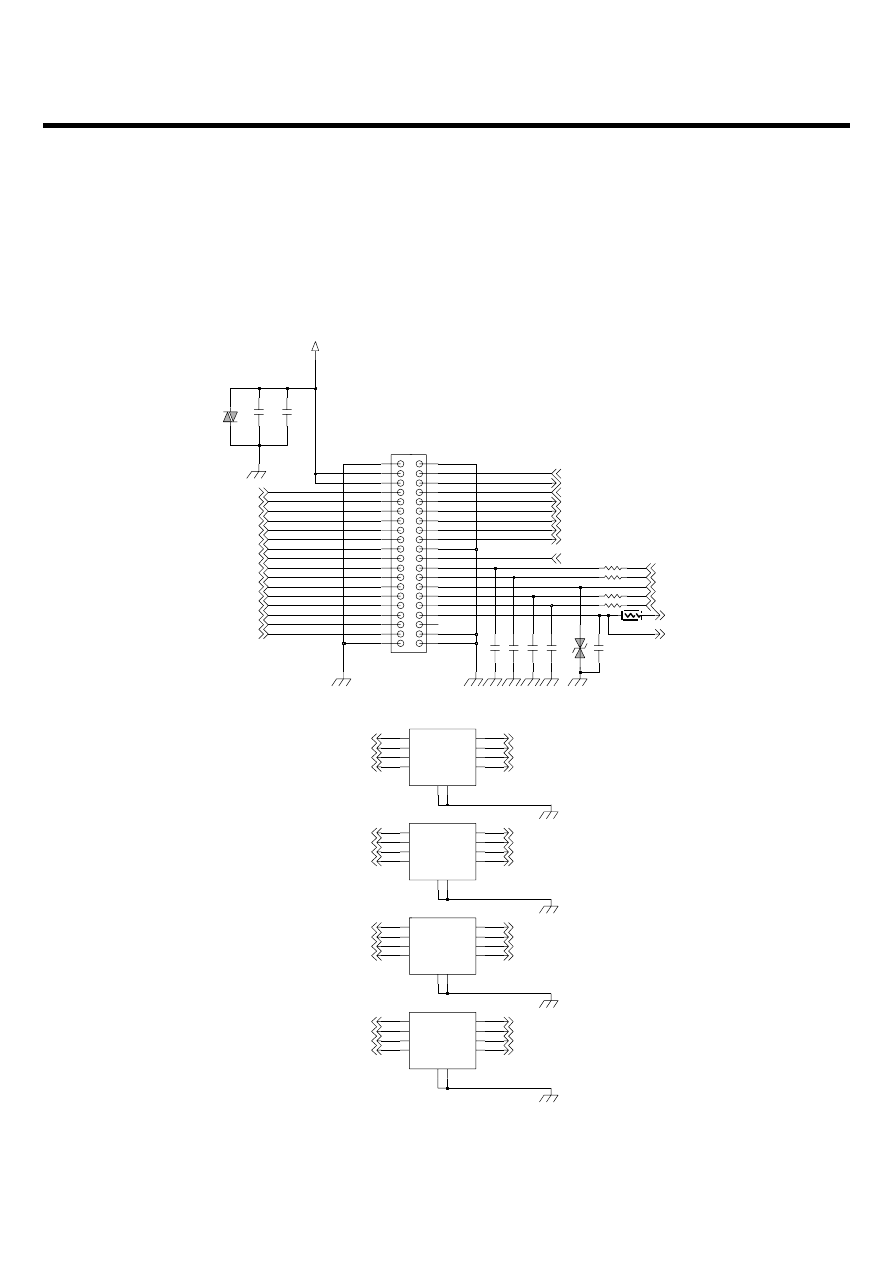
- 66 -
3. TECHNICAL BRIEF
LGE Internal Use Only
Copyright © 2007 LG Electronics. Inc. All right reserved.
Only for training and service purposes
3.10.7 Display
LCD module is connected to Main PCB with 40 pin B TO B connector The LCD module is controlled by
16-bit EBI2 in MSM6280 via Multimedia Chip.
OTP Program Pin
ENBY0036001
1.0T, Socket
GB042-40S-H10-E3000
7
INOUT_B3
INOUT_B4
6
FL301 ICVE10184E150R500FR
G1
5
G2
10
INOUT_A1
1
2
INOUT_A2
INOUT_A3
3
4
INOUT_A4
9
INOUT_B1
INOUT_B2
8
C322
22p
C323
22p
R315
51
22p
C325
VA300
ICVN0505X150FR
25
26
27
28
29
9
21
30
31
32
33
34
35
36
37
38
39
22
40
23
24
12
13
14
15
16
17
18
19
2
20
3
4
5
6
7
8
CN300
1
10
11
VA301
51
R314
NA
C320
C326
22p
G2
1
INOUT_A1
INOUT_A2
2
3
INOUT_A3
INOUT_A4
4
INOUT_B1
9
8
INOUT_B2
INOUT_B3
7
6
INOUT_B4
ICVE10184E150R500FR
FL303
5
G1
10
51
R316
R318
0
5
G1
10
G2
1
INOUT_A1
INOUT_A2
2
3
INOUT_A3
INOUT_A4
4
INOUT_B1
9
8
INOUT_B2
INOUT_B3
7
6
INOUT_B4
ICVE10184E150R500FR
FL300
51
R317
22p
C324
0.1u
C321
6
FL302 ICVE10184E150R500FR
G1
5
G2
10
INOUT_A1
1
2
INOUT_A2
INOUT_A3
3
4
INOUT_A4
9
INOUT_B1
INOUT_B2
8
7
INOUT_B3
INOUT_B4
LCD_VDD_2.8V
LCD_VSYNC_OUT
LCD_MAKER_ID
MMP_LCD_WE_N
MMP_LCD_VSYNC_OUT
WLED_PWR
WLED_2
WLED_4
WLED_5
MMP_LCD_VSYNC_IN
LCD_IF_MODE
LCD_DATA[0]
LCD_DATA[1]
LCD_DATA[2]
LCD_DATA[3]
LCD_DATA[4]
LCD_DATA[5]
LCD_DATA[6]
LCD_DATA[7]
LCD_DATA[14]
LCD_DATA[15]
LCD_DATA[8]
LCD_DATA[9]
LCD_DATA[10]
LCD_DATA[11]
LCD_DATA[12]
LCD_DATA[13]
WLED_1
WLED_3
MMP_LCD_ADS
MMP_LCD_CS_N
LCD_RESET_N
MMP_LCD_RD_N
MMP_LCD_DATA[9]
MMP_LCD_DATA[10]
MMP_LCD_DATA[11]
MMP_LCD_DATA[12]
MMP_LCD_DATA[13]
MMP_LCD_DATA[14]
MMP_LCD_DATA[15]
LCD_DATA[12]
LCD_DATA[13]
LCD_DATA[14]
LCD_DATA[15]
MMP_LCD_DATA[0]
MMP_LCD_DATA[1]
MMP_LCD_DATA[2]
MMP_LCD_DATA[3]
MMP_LCD_DATA[4]
MMP_LCD_DATA[5]
MMP_LCD_DATA[6]
MMP_LCD_DATA[7]
MMP_LCD_DATA[8]
LCD_DATA[0]
LCD_DATA[1]
LCD_DATA[2]
LCD_DATA[3]
LCD_DATA[4]
LCD_DATA[5]
LCD_DATA[6]
LCD_DATA[7]
LCD_DATA[8]
LCD_DATA[9]
LCD_DATA[10]
LCD_DATA[11]
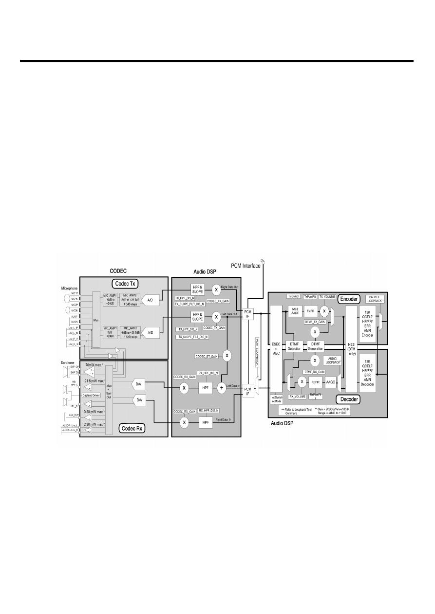
- 67 -
3. TECHNICAL BRIEF
LGE Internal Use Only
Copyright © 2007 LG Electronics. Inc. All right reserved.
Only for training and service purposes
3.10.7.1 Audio Signal Processing & Interface
Audio signal processing is divided uplink path and downlink path.
The uplink path amplifies the audio signal from MIC and converts this analog signal to digital signal
and then transmits it to DBB Chip (MSM6280).
This transmitted signal is reformed to fit in GSM & WCDMA frame format and delivered to RF Chipset.
The downlink path amplifies the signal from DBB chip (MSM6280) and outputs it to receiver (or
speaker). The receive path can be directed to either one of two earphone amplifiers or the auxiliary
output. The outputs earphone1 (EAR1OP, EAR1ON) and auxiliary out (LINE_OP, LINE_ON) are
differential outputs. Earphone2 (HPH_L, HPH_R) is a single-ended output stage designed to drive a
headset speaker.
The microphone interface consists of two differential microphone inputs, one differential auxiliary input
and a two-stage audio amplifier.
Figure. Audio Interface Detailed Diagram(MSM6280)
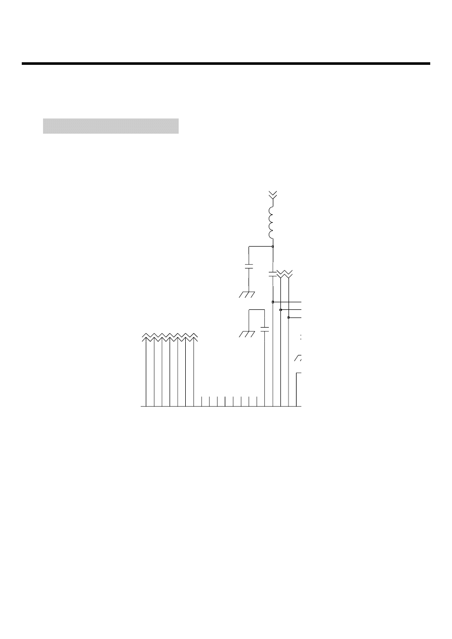
- 68 -
3. TECHNICAL BRIEF
LGE Internal Use Only
Copyright © 2007 LG Electronics. Inc. All right reserved.
Only for training and service purposes
Figure . Audio part schematics
MSM6280 Audio CODEC pins
0.1u
C235
C236
0.1u
L200
100nH
NA
C203
C200
10p
SDCC_DAT
SDCC DAT2
MIC1N
AF20
MIC1P
AE20
AF21
MIC2N
AF22
MIC2P
MICBIAS
T15
LINE_L_IN
AC21
AC22
LINE_L_IP
AC18
LINE_ON
LINE_OP
AC17
AC20
LINE_R_IN
LINE_R_IP
AC19
HPH_L
W17
AA17
HPH_R
HPH_VREF
AA19
EAR1ON
AE18
EAR1OP
AF18
CCOMP
AA20
AF19
AUXIN
AE19
AUXIP
AUXOUT
AA18
HP_R
HP_L
MIC1P
MIC1N
MIC2P
RCV+
RCV-
MICBIAS
SPK_L
SPK_R
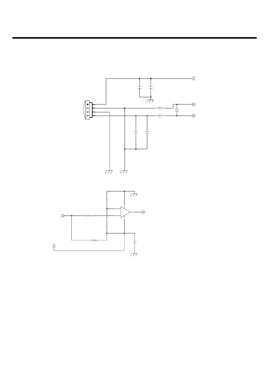
- 69 -
3. TECHNICAL BRIEF
LGE Internal Use Only
Copyright © 2007 LG Electronics. Inc. All right reserved.
Only for training and service purposes
Figure . Audio part schematics
MIC
10u
C563
C568
22n
C569
NA
C564
47p
2
G1
3
G2
1
O
4
P
SPM0204HE5-PB-3
MIC500
33p
C575
10p
C576
C567
22n
MICBIAS
MIC1P
MIC1N
Headset Hook Switch
R905
10K
VREG_MSMP_2.7V
R907
5.1K
C905
0.1u
100K
R906
1M
R904
2
GND
1
OUT
VCC
5
3
VIN+
VIN-
4
U902
NCS2200SQ2T2G
HOOK_SENSE_N
EAR_MIC_P
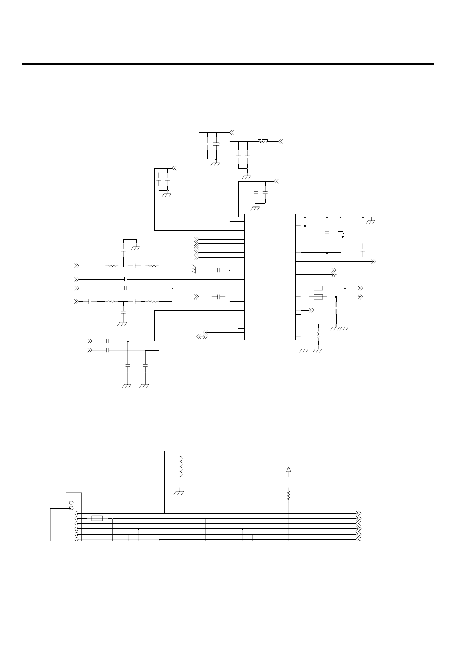
LGE Internal Use Only
Copyright © 2007 LG Electronics. Inc. All right reserved.
Only for training and service purposes
3. TECHNICAL BRIEF
- 70 -
AUDIO DAC/ADC, AMP etc. (WM8983)
Figure . Audio part schematics
FB501
FB500
NA
C550
0.1u
C514
C535
1u
C532
1u
R2_GPIO3
6
RIN
5
4
RIP
ROUT1
29
ROUT2
23
16
SCLK
SDIN
17
27
VMID
DACDAT
10
DBVDD
14
DCVDD
13
12
DGND
L2_GPIO2
3
LIN
2
1
LIP
LOUT1
30
25
LOUT2
7
LRC
11
MCLK
MICBIAS
32
18
MODE
OUT3
22
21
OUT4
33
PGND
U502
ADCDAT
9
28
AGND1
24
AGND2
AUXL
19
AUXR
20
31
AVDD1
AVDD2
26
8
BCLK
15
CSB_GPIO1
4.7u
C520
WM8983
C533
4.7n
R511
18K
R533
0
10u
C525
C534
1u
10u
C513
100K
R519
4.7n
C542
NA
C531
1K
R516
R510
1K
C541
1u
1u
C549
1u
C548
C536
1u
C518
4.7u
C539
1u
12n
C547
C524
0.1u
NA
C544
C519
0.1u
C551
NA
C521
0.1u
C543
NA
12n
C530
18K
R517
C516
4.7u
C517
0.1u
MIC_PWR
MMP_A_MCLK
CODEC_I2C_SCL
CODEC_I2C_SDA
HP_R
HP_L
HP_EAR_L
MIC2P
HP_EAR_R
MID_MICP
SPK_L
SPK_R
FM_AUDIO_L
FM_AUDIO_R
MMP_A_BCLK
MMP_ADO_DACDAT
MMP_A_LRCLK
MMP_ADI_ADCDAT
SPK_OUT-
SPK_OUT+
VREG_5V
VREG_WM_2.7V
VREG_MSME_1.8V
MIDI_3.3V
19
2
21
3
4
5
6
7
CN500
1
R528
100K
FB504
VREG_MSMP_2.7V
2.2uH
L504
TV_OUT
EAR_MIC_P
RMT_INT-USB_D+
FM_ANT
MIDI_EAR_L
MIDI_EAR_R
3.10.7.2 Audio Mode
There are three audio modes (Voice call, speaker phone, MIDI/MP3).
Audio & Sound Main Component
There are 8 main components in KU990.
LGE Internal Use Only
Copyright © 2007 LG Electronics. Inc. All right reserved.
Only for training and service purposes
3. TECHNICAL BRIEF
- 71 -
Table. Audio Mode
Table. Audio main component list
Headset MP3
Headset
Headset MIDI Bell
Headset
Speaker MP3
Loud Mode
MP3
Speaker MIDI Bell
Loud Mode
MIDI
Speaker Phone
Loud Mode
Headset Voice Call
Headset
Speaker Phone
Loud Mode
Speaker phone
Receiver Voice Call
Description
Receiver Mode
Voice Call
Device
MODE
-42 dB microphone
SPOB-413S42-
RC3310BC
CAM MIC
7
32 ohm receiver
EMR0906SP
Receiver
5
8 ohm Speaker
EMS1634APB1
Speaker
4
-42 dB microphone
SPM0204HE5-PB
Main MIC
6
Ear MIC
HC-MQD-LG059
Ear MIC
8
Analog Switch for MIC BIAS
NC7SB3157L6X
Analog Switch
3
ADC/DAC, AB class SPK AMP
Base-Band Modem
Note
WM8983
MSM6280
Maker Part No.
Audio Codec
MSM6280
Component
2
1

LGE Internal Use Only
Copyright © 2007 LG Electronics. Inc. All right reserved.
Only for training and service purposes
3. TECHNICAL BRIEF
- 72 -
# Multimedia Chip
3.11 Feature List
3.11.1 IC Characteristics
• MCP with Internal SDRAM, no need for external memory.
• Package: 180-pin TFBGA (8 x 8 mm)
• 90nm process
• Core voltage - 1.0 V
• IO voltage - Eleven strips, separate voltage between 1.8 and 3.3 V
3.11.2 Multimedia Performance
• Digital Still Camera support with ISP on chip up to 5M pixel.
- Photo-album and photo-editing capabilities.
- Superior quality, (e.g. including lens shading).
- Camera controls for flash, optical zoom,focus, shutter and iris.
• Camcorder operation as a DivX recorder /player at 30 fps CIF, VGA resolution.
AVI file format with MP3 audio.
• Player for general DivX content, up to 30 fps CIF resolution. MP3 or WMA audio.
• 3GPP MMS compliant video clip recorder, supporting CIF/QCIF H.263, MPEG4 recording with AMR
voice or AAC audio.
• Player for 3GPP MMS / streaming video clips, up to 30 fps CIF H.263, MPEG4, and H.264 with AMR
voice or AAC/Enhanced AACPlus audio.
• 3GPP-compliant videophone, with H.263 or MPEG4 video at QCIF 15 fps (full-duplex).
• MIDI player (for ring tones, melodies).
Compliant with 3GPP standards, including
support for Mobile XMF for melodies with custom instruments.

LGE Internal Use Only
Copyright © 2007 LG Electronics. Inc. All right reserved.
Only for training and service purposes
3. TECHNICAL BRIEF
- 73 -
• Audio stereo recorder player MP3/WMA
• ID3 tags display
• Spectral bars
• Lyrics display
• Equalizer
• 3D Surround Audio
3.11.3 DRM
• MDTV Conditional access compliant to JSR-177 (AES and TDES)
• Key exchange support
• True RNG (Random Number Generator)
3.11.4 3D Graphics
• 3D hardware + software accelerator targeting VGA 30 fps games with PlayStation
TM
-1 enhanced
quality.
- Setup and viewport transforms
- Bilinear and Trilinear texturing
- Multi-texturing
- Flat and Gourard shading
- 24-bit ARGB support
- Compressed textures (2 bits/texel)
- Mipmaping
- Full scene anti-aliasing (x4 / x16)
- 16-bit Z-buffer
- 4-bit stencil buffer
- Fog
- Alpha blending
- Dot3 bump mapping
• Fill rate: 120M pixels/sec
• Polygon rate 0.8M triangles/sec

LGE Internal Use Only
Copyright © 2007 LG Electronics. Inc. All right reserved.
Only for training and service purposes
3. TECHNICAL BRIEF
- 74 -
3.11.5 Image Sensor
• 10/12/14/16-bit RGB - Bayer Grid
- CMOS up to 5MP
- CCD up to 5MP
- Pixel clock - Up to 90 MHz.
- Active pixel rate - up to 75M pixels/sec:
- 15fps @ 5MP
- 25fps @ 3MP
- 30fps @ 2MP
- Black-level evaluation and correction
- Defective pixel correction
- Auto exposure and White-balance
- Edge enhancement and auto focus.
- Lens shading correction
- Polyphase image scaling.
- Digital zoom up to X4 in 16 steps
- 8/16-bit YCbCr - 4:2:2
- Input streaming bus - as CCIR601
- Progressive (CMOS/CCD sensors) or interlaced (PAL/NTSC decoders) mode
- Pixel clock - Up to 120 MHz (8-bit), 60Mhz (16-bit)
- Input resolution - Up to 5M pixels
- Auto focus
- Polyphase image scaling
- Digital zoom up to X4 in 16 steps
3.11.6 LCD Port
• Output resolution - up to VGA
• Supports dual-panels (two LCDs)
• Bypass from Host port to LCD CPU bus
• Up to 18-bit color depth (262K colors)
• CPU bus 8/9/16/18 bit compliant to all known vendors.
• RGB bus 3/6/18 bit up to 30Mhz clock
3.11.7 TV-out Port
• Composite analog interface
- NTSC-M
- PAL-B,D,G,H,I

LGE Internal Use Only
Copyright © 2007 LG Electronics. Inc. All right reserved.
Only for training and service purposes
3. TECHNICAL BRIEF
- 75 -
3.11.8 Video and Graphics Postprocessing
• Handles Video (YUV) and Graphic (RGB)
• Video de-blocking
• Blending of video and graphics - up to 256 levels of blending
• Resizing (upscale and downscale) using quality polyphase filter
• Rotation and flip - 90, 180 and 270 degrees
• Picture brightness, contrast, and saturation control
• Display gamma adjustment
• Color space reduction
3.11.9 Serial Audio Ports
• ZR3453X has two audio/voice ports: one port is used for host bypass connection, and another for
connecting to a codec or to a Bluetooth voice port.
- PCM master/slave
- I2S master/slave (5 lines including clock)
- AC’97 master (5 lines including AC-Link reset)
- Audio output master clock (I2S), up to 48 MHz
- Supports sample rates of 8, 11.025, 16, 22.05, 24, 32, 44.1 or 48 kHz
3.11.10 Serial Data Ports
• I2C Multiple device support 100 and 400 kHz
• UART with flow control up to 3Mb/sec
• SPI port with Bit clock up to 40 MHz
- (Motorola, National microwire, TI synchronous serial interface )
3.11.11 Mass Storage
• High-speed SD/MMC I/F
• NAND-flash storage
• SPI-flash
• CE-ATA HDD.
• SDIO peripherals

LGE Internal Use Only
Copyright © 2007 LG Electronics. Inc. All right reserved.
Only for training and service purposes
3.11.12 USB
• USB 2.0 High speed/full speed
• USB On The Go
• USB applications:
- USB mass storage
- PictBridge
- Webcam
3.11.13 Host Port
• Two flavors:
- Generic interface 8/16-bit Intel style.
Connects as memory map (4-bit address)
- LCD like 8/9/16 bit multiplexed bus.
Connects as an LCD (1-bit address)
3.11.14 Clocks
• Main clock input frequency, 10 to 31 MHz:
- Directly from system PMU main clock and bypass its control
- Embedded crystal oscillator (12Mhz)
- Optional GPS TCXO
• Four configurable clock-out pins to drive external components:
(e.g. Audio codec, Sensor, PWM)
3.11.15 Boot
• Host boot
• Standalone boot
3.11.16 Debug
• JTAG for code debug
• UART for fast system ramp up
3.11.17 Power
• Very low power consumption, smaller than150mW for all intense multimedia applications.
• Low power sleep mode 100 µW
- Host can control display audio and peripherals via bypass
• Light sleep mode 500uW
- Specifically for GPS accurate off-line tracking
3. TECHNICAL BRIEF
- 76 -
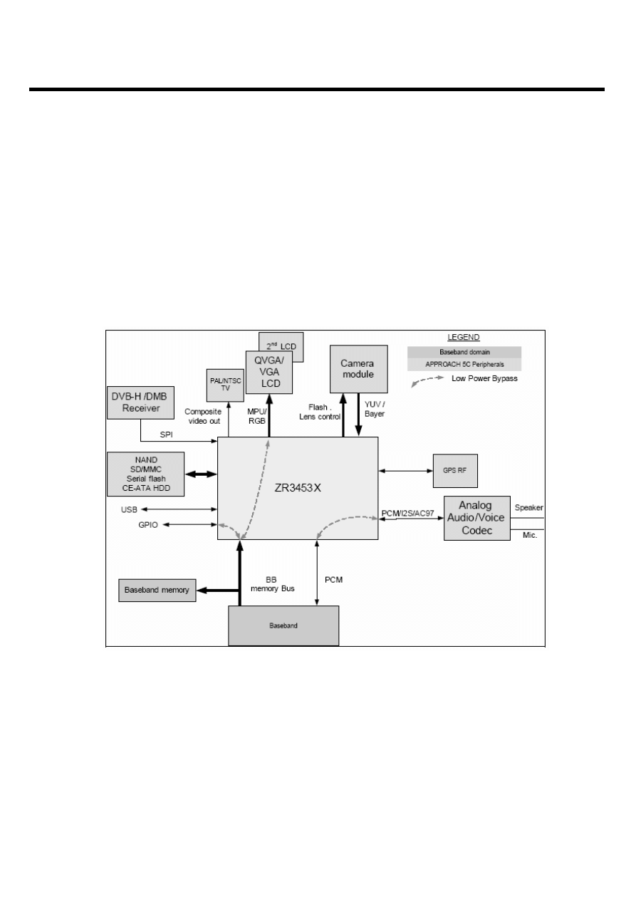
LGE Internal Use Only
Copyright © 2007 LG Electronics. Inc. All right reserved.
Only for training and service purposes
3. TECHNICAL BRIEF
- 77 -
Figure 1-1 presents a typical multimedia cellular phone system where ZR3453X is used as a co-
coprocessor. In this system, ZR3453X is connected to the following devices:
• Baseband chip (the host)
• CCD/CMOS Image Sensor for capturing video and still
• LCD panel(s)for displaying video
• Audio CODEC (A2D, D2A) for capturing voice and playing voice/music
• Media Flash (SmartMedia, NANDFlash, MMC or SD) to store media data (two active I/F, e.g. one
NAND and one SD)
• Connector to TV
[ Figure 1-1 ]
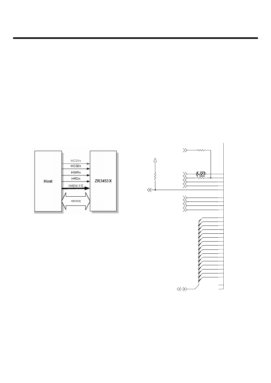
LGE Internal Use Only
Copyright © 2007 LG Electronics. Inc. All right reserved.
Only for training and service purposes
3.12 Multimedia Chip Interface
3.12.1 Host Interface
3.12.1.1 Host Interface
The HOST interface connects the ZR3453X and the host processor
(a handset baseband
chip) in two optional modes:
• On the host memory bus.
• On the host LCD bus.
3. TECHNICAL BRIEF
- 78 -
VREG_MSMP_2.7V
M13
NCSN
L13
HGINTN
A7
B7
HRDN
HWRN
B9
HD0
D12
HD1
C10
B12
HD10
A12
HD11
HD12
B11
A11
HD13
HD14
C9
B10
HD15
HD2
C12
C13
HD3
C14
HD4
HD5
B14
HD6
C11
B13
HD7
A14
HD8
HD9
A13
A10
HA11
HA12
A9
C8
HA13
C7
HA14
HCS0N
B8
HCS1N
A8
10K
R310
R311
0
NA
R313
NA
R309
MMP_CS_N
MMP_INT_N
MMP_LCD_BYPASS_CS_N
NAND_ALE
EBI2_ADDR[11]
EBI2_ADDR[13]
EBI2_ADDR[14]
EBI2_DATA[0:15]
EBI2_DATA[15]
EBI2_DATA[14]
EBI2_DATA[13]
EBI2_DATA[12]
EBI2_DATA[11]
EBI2_DATA[10]
EBI2_DATA[9]
EBI2_DATA[8]
EBI2_DATA[7]
EBI2_DATA[6]
EBI2_DATA[5]
EBI2_DATA[4]
EBI2_DATA[3]
EBI2_DATA[2]
EBI2_DATA[1]
EBI2_DATA[0]
EBI2_ADDR[12]
EBI2_OE_N
EBI2_WE_N
[ Block Diagram ]
[ Schematics ]
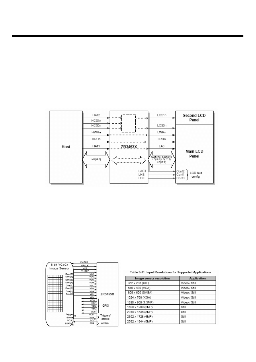
LGE Internal Use Only
Copyright © 2007 LG Electronics. Inc. All right reserved.
Only for training and service purposes
3. TECHNICAL BRIEF
- 79 -
3.12.2 Host - LCD - Bypass mode
The Host-LCD Bypass bypasses the host interface pins to the LCD pins.
This means that the bus transactions performed by the host are transferred to the LCD pins, enabling
the host to have full control over one or two LCD panels, even when the ZR3453X is in sleep mode.
This is the default mode.
3.12.3 Camera interface
ZR3453X connects with the CCD or CMOS Image Sensor (CIS) via its image sensor port.
ZR3453X supports several system configurations:
• CCD bayer 10,12,14,16 bit (ZR34532 only)
• CMOS bayer 10,12,14,16 bit
• YCbCr 8 bit
• YCbCr 8 bit with pixel valid
• YCbCr 16 bit
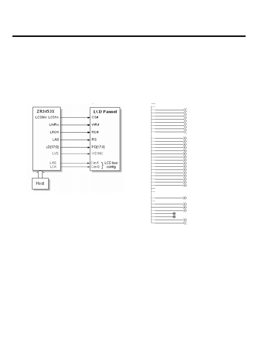
LGE Internal Use Only
Copyright © 2007 LG Electronics. Inc. All right reserved.
Only for training and service purposes
3.12.4 LCD Interface
The ZR3453X LCD port supports mobile LCD panels of upto VGA size and upto 60fps refresh rate.
There are various bus formats and color depth up to 18-bit (262K colors).
3. TECHNICAL BRIEF
- 80 -
[ Block Diagram ]
M9
VIDP
VIDH
P11
N12
VIDI
N7
VIDJ
VIDK
L8
P13
VIDL
L9
VIDM
VIDN
N13
VIDO
M11
E3
LVS
C4
LWRN
LD12
C1
LD13
C2
C5
LD14
LD15
C6
D3
LD16
LD17
D1
B6
LD2
LD3
B4
LD4
A4
C3
LD5
A3
LD6
LD7
A2
A1
LD8
LD9
B2
E4
LHS
LRDN
D5
D4
LA0
LACT
E2
LCK
E1
A6
LCS0N
LCS1N
D2
LD0
B5
A5
LD1
LD10
B1
B3
LD11
TP301
TP300
MMP_LCD_CS_N
MMP_LCD_ADS
MMP_LCD_RD_N
MMP_LCD_WE_N
MMP_LCD_VSYNC_IN
MMP_LCD_VSYNC_OUT
MMP_LCD_DATA[15]
MMP_CAM_DATA[7]
MMP_CAM_DATA[6]
MMP_CAM_DATA[5]
MMP_CAM_DATA[4]
MMP_CAM_DATA[3]
MMP_CAM_DATA[2]
MMP_CAM_DATA[1]
MMP_CAM_DATA[0]
MMP_LCD_DATA[0]
MMP_LCD_DATA[1]
MMP_LCD_DATA[2]
MMP_LCD_DATA[3]
MMP_LCD_DATA[4]
MMP_LCD_DATA[5]
MMP_LCD_DATA[6]
MMP_LCD_DATA[7]
MMP_LCD_DATA[8]
MMP_LCD_DATA[9]
MMP_LCD_DATA[10]
MMP_LCD_DATA[11]
MMP_LCD_DATA[12]
MMP_LCD_DATA[13]
MMP_LCD_DATA[14]
[ Schematics ]
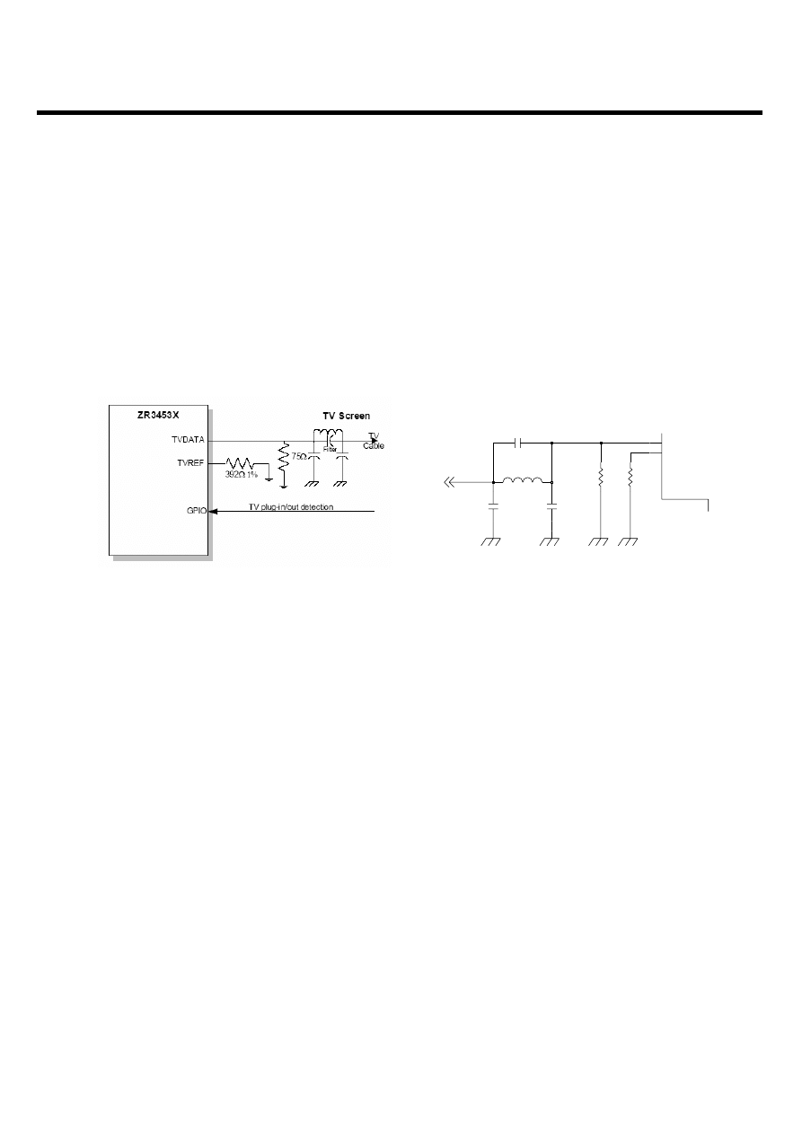
LGE Internal Use Only
Copyright © 2007 LG Electronics. Inc. All right reserved.
Only for training and service purposes
3. TECHNICAL BRIEF
- 81 -
3.12.5 TV out Interface
The display data is converted to video with video-encoder according to CCIR-601 and sampled by 10-
bit DAC and transmitted over an analog pad as a composite video signal.
This mode is used in a system where ZR3453X is connected gluelessly to a TV screen that requires
real-time display data. ZR3453X generates TV signal according to the NTSC and PAL standards.
The TVDATA pin can drive a full video level signal directly into a 75 terminated TV cable.
[ Block Diagram ]
392ohm 1%
330p
C335
E13
VENBYPIN
TVDATA
G14
TVREF
F13
22p
C331
R339
390
330p
C334
R338
75
2.2uH
L300
TV_OUT
[ Schematics ]
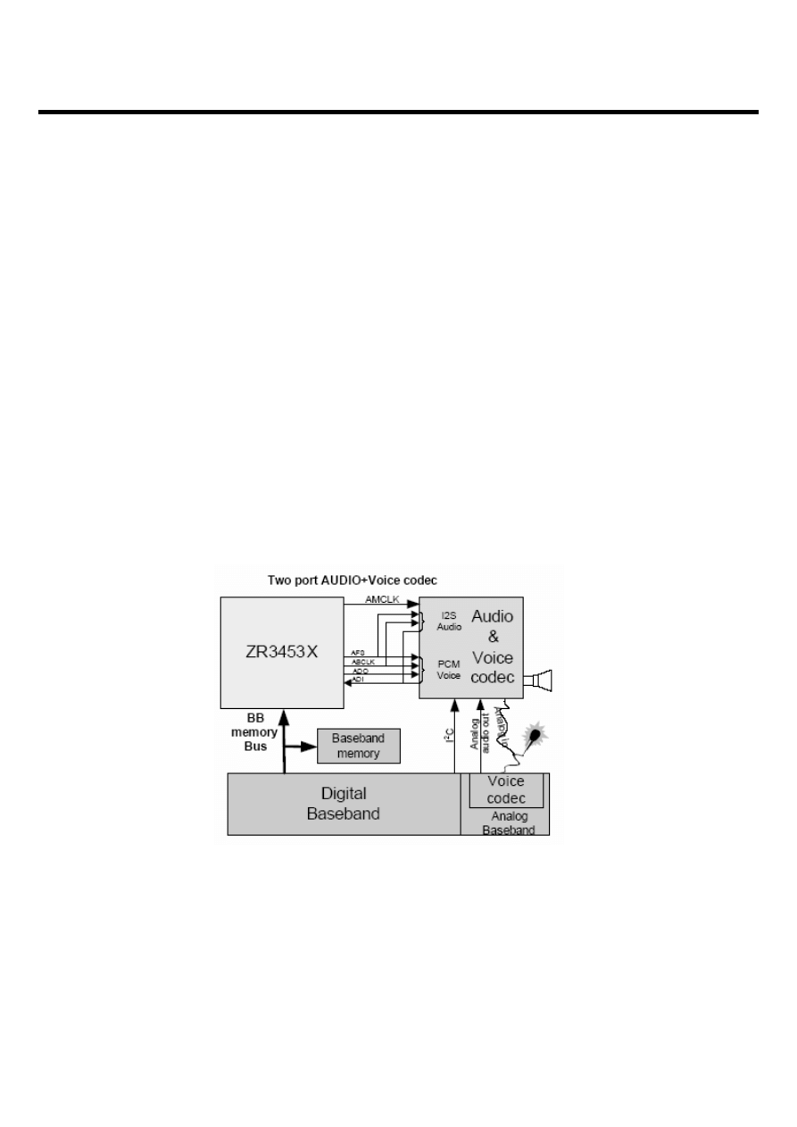
- 82 -
3. TECHNICAL BRIEF
3.12.6 Audio Interface
In this configuration ZR3453X is connected to an external audio codec.
There are three possible configurations:
• Audio/Voice codec with two ports: PCM and I2S
• Audio/Voice codec with one port: I2S
• Audio/voice/data codec with one port: AC97
In all configurations ZR3453X connects its external audio ports to the codec single or two
ports.
The host uses its internal voice codec for voice communication. There is no bypass of voice.
The host controls the codec configuration via I2C bus directly. The host codec analog audio output is
connected to the external audio codec and muxed with the codec audio path from the ZR3453X on the
way is to the speaker.
The microphone is connected to the external audio codec and the baseband internal codec.
ZR3453X appears in Figure 3-35 as a master on the bit clock and frame sync. This is only one of the
possible configurations. In external audio configuration ZR3453X can run all the Audio/voice
applications including conversation recording .
LGE Internal Use Only
Copyright © 2007 LG Electronics. Inc. All right reserved.
Only for training and service purposes
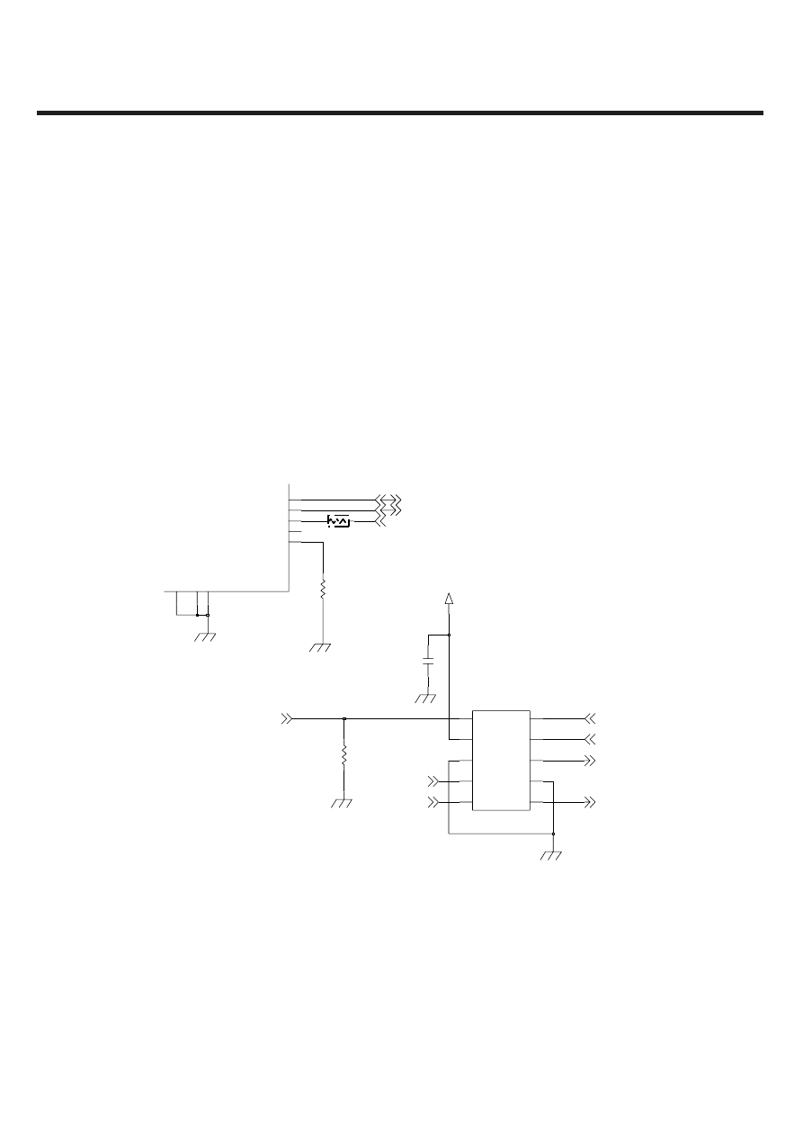
- 83 -
3. TECHNICAL BRIEF
3.12.7 USB interface
ZR3453X is a USB 2.0 Device or On-the-Go dual-role device (OTG) with the following
characteristics:
• Complies with USB (
Universal Serial Bus) 2.0 specifications
• Complies with On-the-Go Supplement 1.0a
• Integrated 45-ohm termination, 1.5Kilohm pull-up and 15-Kilohm pull-down resistors.
• Supports 480-Mbps high-speed, 12-Mbps full-speed and 1.5Mbps low-speed (Host mode only) data
transmission rates.
• Control + 4 endpoints:
- EP0 - two-way Control
- 2-input , 2-output - Bulk, INT or ISO
• Suspend, resume, reset and SOF signaling
LGE Internal Use Only
Copyright © 2007 LG Electronics. Inc. All right reserved.
Only for training and service purposes
3.4K
1%
UDN
P4
P3
UDP
P6
UID
URSET
M7
J4
UVBUS
L5
AGND_USBC
K5
AGND_USBT
F12
AGND_VDAC
R340
3.3K
R335
0
MMP_USB_D+
MMP_USB_D-
VREG_5V
+VPWR
100K
R345
U304
D+
3
D-
5
GND
4
1
HSD1+
7
HSD1-
2
HSD2+
HSD2-
6
SEL
10
9
VCC
8
_OE
FSUSB30UMX
0.01u
C336
USB_SELECT_N
MSM_USB_D-
MMP_USB_D-
USB_D+
USB_D-
MSM_USB_D+
MMP_USB_D+
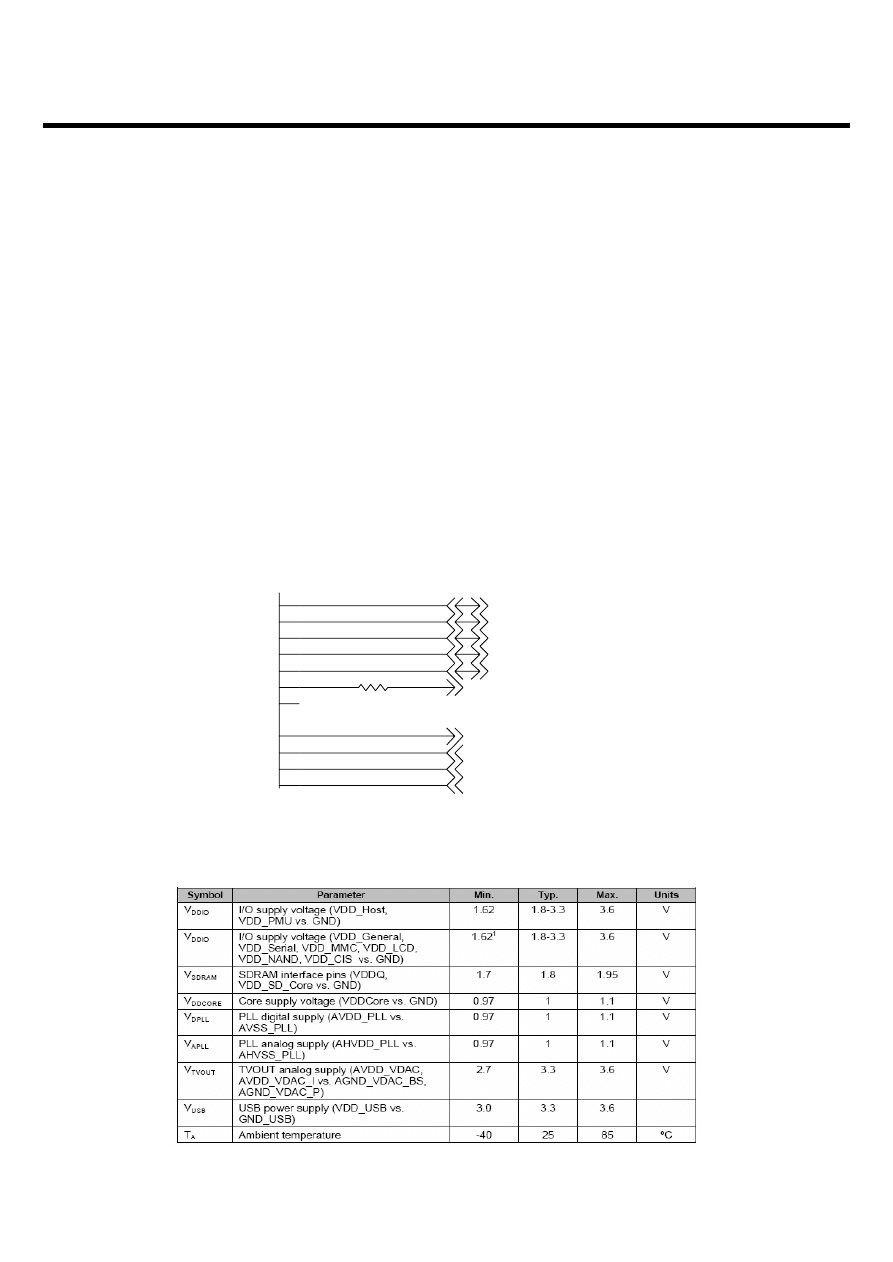
- 84 -
3. TECHNICAL BRIEF
3.12.8 MMC interface
ZR3453X has a dedicated port for multimedia cards. It can support SD (Secure Digital) cards and
SecureMMC (standard multimedia cards with security functions).
The same port can be used for HDD CE_ATA connection or SDIO to peripheral devices
(e.g.; MDTV front-end).
MMC
• MMC v4
• Dual voltage (separate IO power domain, host GPIO control)
• 1 or 4 bit cards
• Multiple cards support (if dual-voltage or high-speed interface are not used)
• Up to 43 MHz bit clock
SD
• 1 or 4 bit bus support
• High-Speed SD, up to 43 MHz bit clock
3.12.9 Power Domain
LGE Internal Use Only
Copyright © 2007 LG Electronics. Inc. All right reserved.
Only for training and service purposes
VMCLK
P12
P10
VPCLK
VVS
K12
M12
VHREF
SCLK
G1
H2
SCMD
SDAT0
F1
SDAT1
F2
SDAT2
E5
F3
SDAT3
G3
SWP
R312
33
MMP_CAM_MCLK
MMP_CAM_HSYNC
MMP_CAM_PCLK
MMP_CAM_VSYNC
MMP_MICROSD_CLK
MMP_MICROSD_DATA[3]
MMP_MICROSD_DATA[2]
MMP_MICROSD_DATA[1]
MMP_MICROSD_DATA[0]
MMP_MICROSD_CMD
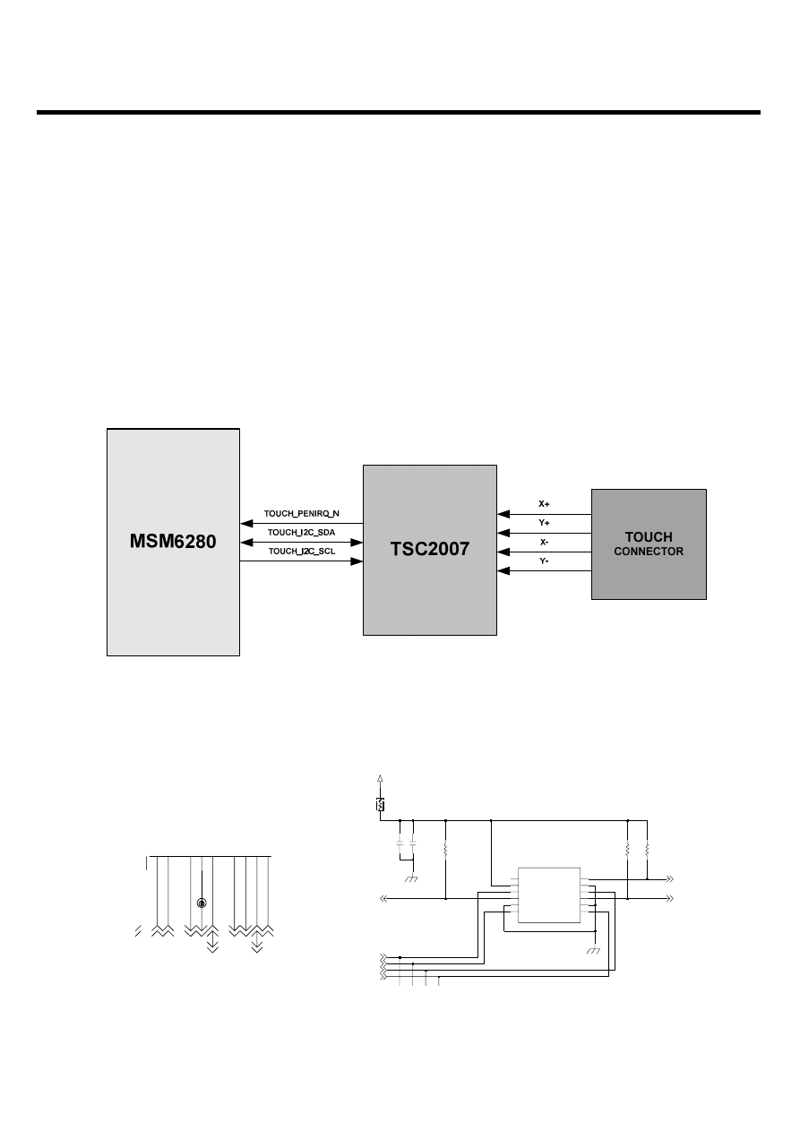
- 85 -
3. TECHNICAL BRIEF
3.13 Touch Screen Interface
The TSC2007 device has a 12-bit analog-to-digital resistive touch screen converter including drivers
and the control logic to measure touch pressure. The TSC2007 device is controlled by I2C port from
MSM6280.
Touch Screen interface scheme is shown in Figure.
And, there control signals are followed
• TOUCH_I2C_SCL : I2C CLOCK
• TOUCH_I2C_SDA : I2C DATA
• TOUCH_PENIRQ_N : DETECT
LGE Internal Use Only
Copyright © 2007 LG Electronics. Inc. All right reserved.
Only for training and service purposes
Figure. Touch Screen Interface
TP200
G6
UART2_CTS_N_GPIO90
UART2_DP_TX_DATA_GPIO88
E4
UART2_RFR_N_GPIO91
F4
L23
UART3_CTS_N_GPIO86
M21
UART3_DP_RX_DATA_GPIO85
UART3_DP_TX_DATA_GPIO84
M19
F14
GPIO64
GPIO39
F7
GPIO40
D6
D7
GPIO44
D8
VGA_CAM_PWR_EN
UART_TXD
TOUCH_I2C_SCL
TOUCH_PENIRQ_N
TOUCH_I2C_SDA
CAM_MODE2_N
USIM_DATA
PM_INT_N
USIM_CLK
USIM_RST_N
0
R700
A0
A1
C2
A1
AUX
GND
D2
PENIRQ-
B1
D1
SCL
C1
SDA
VDD_REF
A2
A3
X+
C3
X-
B3
Y+
D3
Y-
TSC2007IYZGR
U700
B2
0.1u
LCD_VDD_2.8V
C701
R703
2.7K
NA
R702
C700
1u
2.7K
R704
X-
Y-
Y+
X+
TOUCH_PENIRQ_N
TOUCH_I2C_SCL
TOUCH_I2C_SDA

- 86 -
3. TECHNICAL BRIEF
3.14 Main Features
1. Main features of KU990
- BAR Type
- WCDMA(2100) + GSM(900,1800) + PCS(1900) Triple mode
- Main LCD: 240x400/3.0”/262K TFT
- 5.1M Pixel AF Camera
- VGA CMOS Camera
-
φ16 module speaker
- Stereo Headset
- Video telephony in WCDMA with camera
- HSDPA up to 3.6 Mbps
- Loud Speaker phone(in GSM and WCDMA)
- 64 Poly Sound
- Audio: MP3, AAC, AAC+,AAC++, WMA, WAV
- MPEG4 encoder/decoder and play/save
- H.263 decoder
- Video Recording: VGA 30 fps
- JPEG en/decoder
- Support Bluetooth, USB
- FM Radio
- touch screen, touch feedback
- 103 x 54 x 15.6 mm
- 1000mAh soft pack
LGE Internal Use Only
Copyright © 2007 LG Electronics. Inc. All right reserved.
Only for training and service purposes
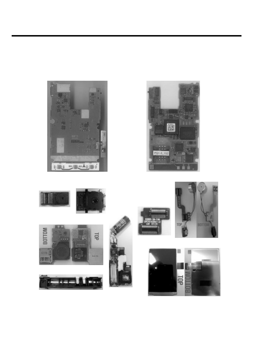
- 87 -
3. TECHNICAL BRIEF
2. Main Components of KU990
LGE Internal Use Only
Copyright © 2007 LG Electronics. Inc. All right reserved.
Only for training and service purposes
LCD
MAIN Bottom Side
MAIN Top Side
5M camera
VGA camera
VGA Camera FPCB
Intenna
Strobe Flash
Sub PCB
5M Camera FPCB
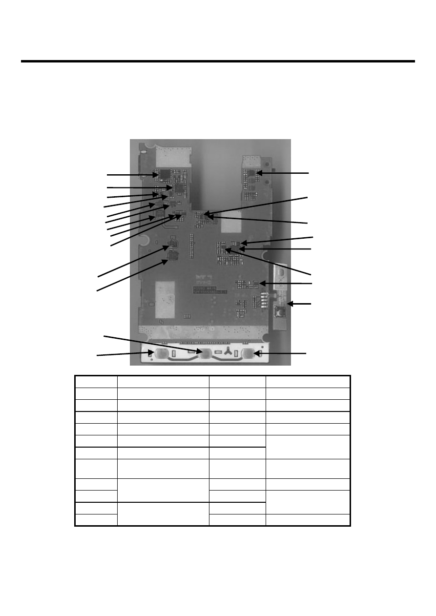
- 88 -
3. TECHNICAL BRIEF
2.1 Main Top Side
LGE Internal Use Only
Copyright © 2007 LG Electronics. Inc. All right reserved.
Only for training and service purposes
Switch IC for 5M VT Call
U607
U602
U604
MicroSD Select MSM and
MMP IC
U400
VGA CAM LDO IC
U600
5M CAM LDO IC
U601
LCD Backlight Charge
Pump IC
U301
Over Voltage Protection IC
U505
Touch Screen Driver IC
U700
U401
U300
Switch IC for USB2.0
U304
Side Key FPCB
SideKey
Audio AMP LDO
U503
LCD LOD IC
U303
USB/REMOCON SEL IC
U507
End Key
END
CAM/HP MIC SEL IC
U506
Clear Key
701
Headphone AMP IC
U504
Send Key
700
FM Radio IC
U103
Description
Reference
Description
Reference
U103
U504
U506
U503
U507
U304
U505
U601
U602
U400
U401
701
700
END
SideKey
U303
U300
U301
U600
U607
U604
U700
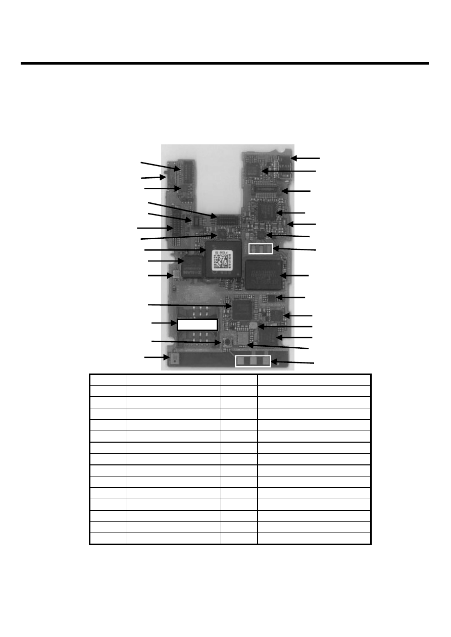
- 89 -
3. TECHNICAL BRIEF
2.2 Main Bottom Side
LGE Internal Use Only
Copyright © 2007 LG Electronics. Inc. All right reserved.
Only for training and service purposes
PAM IC for GSM
U101
USIM Connector
J400
Memory IC
U402
MSM6280 Modem IC
U200
Antenna Switching Module
FL100
RF Switch
SW100
PAM IC for WCDMA
U105
27Mhz Crystal Oscillator
X300
Duplexer IC for WCDMA
FL103
RTR6275 RF IC
U100
Main Intenna Connection PAD
ANT PAD
MIC
MIC500
Battery Connector PAD
OUT PAD
DC-DC Converter IC
U701
19.2MHz Crystal Oscillator for TCXO
X100
ZR3453 DSP IC
U302
Charging IC
U500
LCD Connector
CN300
PM6650 PMIC
U501
5M CAM FPCB Connector
CN600
32.768KHz Crystal Oscillator
X500
Strobe Flash Connector
CN601
Main-Sub B-to-B Connector
CN603
Linear Motor Driver IC
U606
WM8983 Audio DAC/ADC AMP IC
U502
Mode Switch
SW600
TA and USB Connector
CN500
VGA CAM FPCB Connector
CN701
Description
Reference
Description
Reference
SW600
CN701
U606
CN300
CN601
CN600
U701
U200
U302
X300
J400
MIC500
SW100
U100
FL100
ANT PAD
U101
FL103
U105
X100
U402
OUT PAD
U500
X500
U501
CN603
CN500
U502
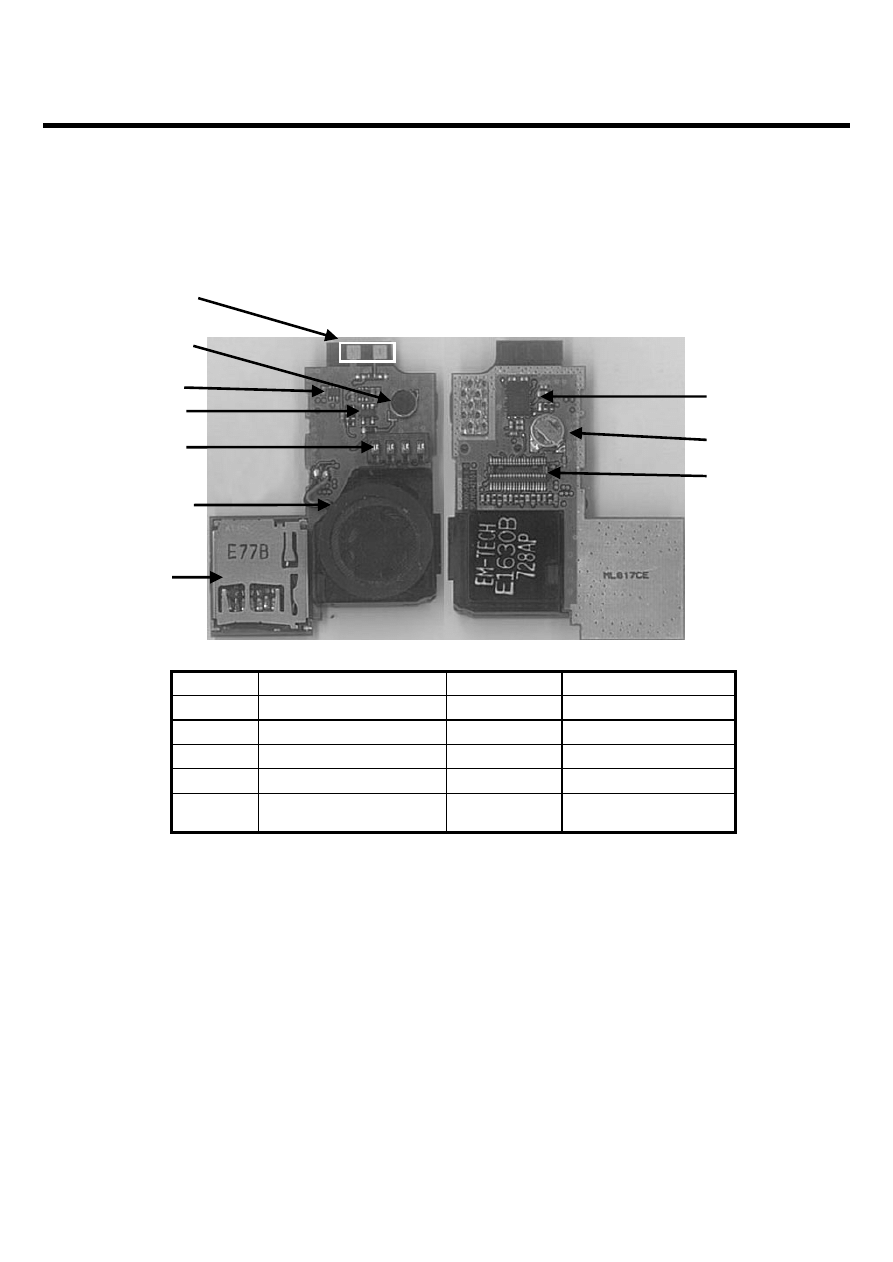
- 90 -
3. TECHNICAL BRIEF
2.3 Sub PCB
LGE Internal Use Only
Copyright © 2007 LG Electronics. Inc. All right reserved.
Only for training and service purposes
Main-Sub B-to-B
Connector
CN801
Wheel Switch Connector
CN800
Backup Battery
BAT900
Headset Hook Switch IC
U902
Bluetooth Driver IC
M800
5MP Camera Power IC
U900
T-Flash Connector
S800
CAM MIC
MIC900
Module Speaker
SPEAKER
Bluetooth Antenna PAD
BT PAD
Description
Reference
Description
Reference
S800
SPEAKER
CN800
U902
U900
BT PAD
MIC900
CN801
BAT900
M800
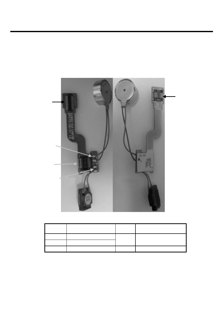
- 91 -
3. TECHNICAL BRIEF
LGE Internal Use Only
Copyright © 2007 LG Electronics. Inc. All right reserved.
Only for training and service purposes
2.4 VGA Camera FPCB
Vibrator PAD
Vibrator
Touch Window Connector
CN102
VGA_CAMERA Connector
CN100
Main B-to-B Connector
(FPCB to Main PCB)
CN101
Receiver PAD
Receiver
Description
Reference
Description
Reference
CN100
CN101
Receiver
Vibrator
CN102
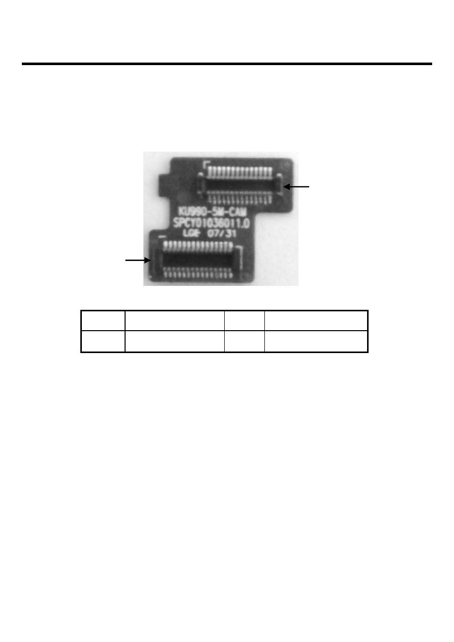
- 92 -
3. TECHNICAL BRIEF
LGE Internal Use Only
Copyright © 2007 LG Electronics. Inc. All right reserved.
Only for training and service purposes
2.5 5M Camera FPCB
Main PCB Connector
(FPCB to Main PCB)
CN602
5M Camera Module
Connector
CN601
Description
Reference
Description
Reference
CN602
CN601
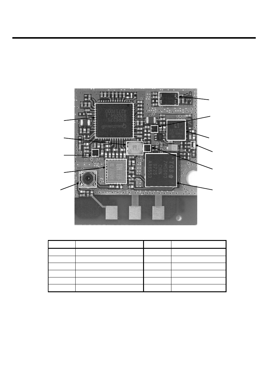
- 93 -
4. TROUBLE SHOOTING
4. TROUBLE SHOOTING
LGE Internal Use Only
Copyright © 2007 LG Electronics. Inc. All right reserved.
Only for training and service purposes
4.1 RF Component
Reference Description
Reference
Description
U100
GSM/UMTS Transceiver (RTR)
X100
VCTCXO(19.2MHz)
FL103
UMTS Duplexer
FL104
UMTS TX SAW
FL102
UMTS RX SAW
U105
UMTS PAM
FL100 Front -End-Module
U104 Coupler
SW100
RF Antenna Connector
FL101
GSM900 TX SAW
U101 GSM/EDGE
PAM
FL100
SW100
FL102
FL103
U100
U101
FL101
U104
U105
FL104
X100
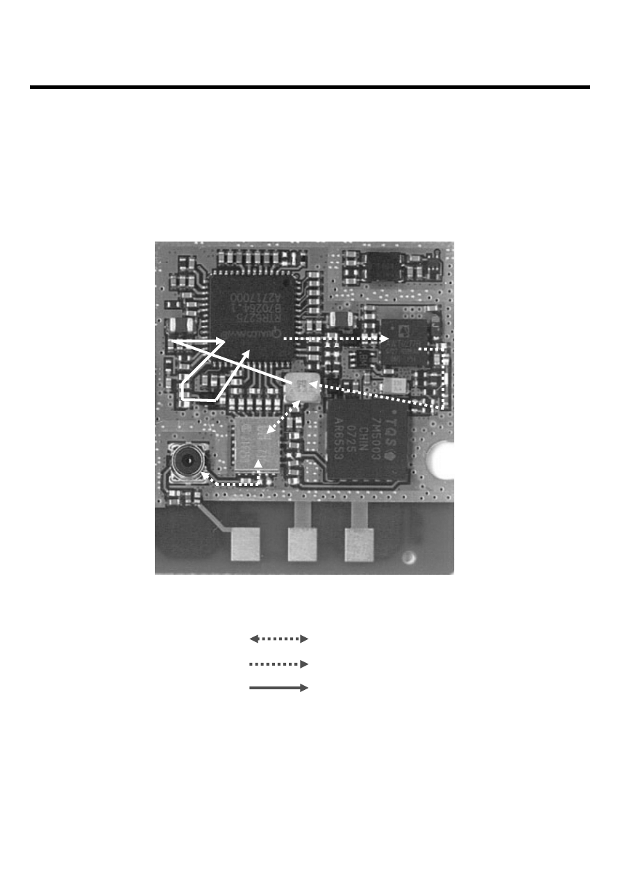
- 94 -
4. TROUBLE SHOOTING
LGE Internal Use Only
Copyright © 2007 LG Electronics. Inc. All right reserved.
Only for training and service purposes
4.2 SIGNAL PATH
4.2.1 UMTS PATH
COMMON TX/RX PATH
UMTS TX PATH
UMTS RX PATH
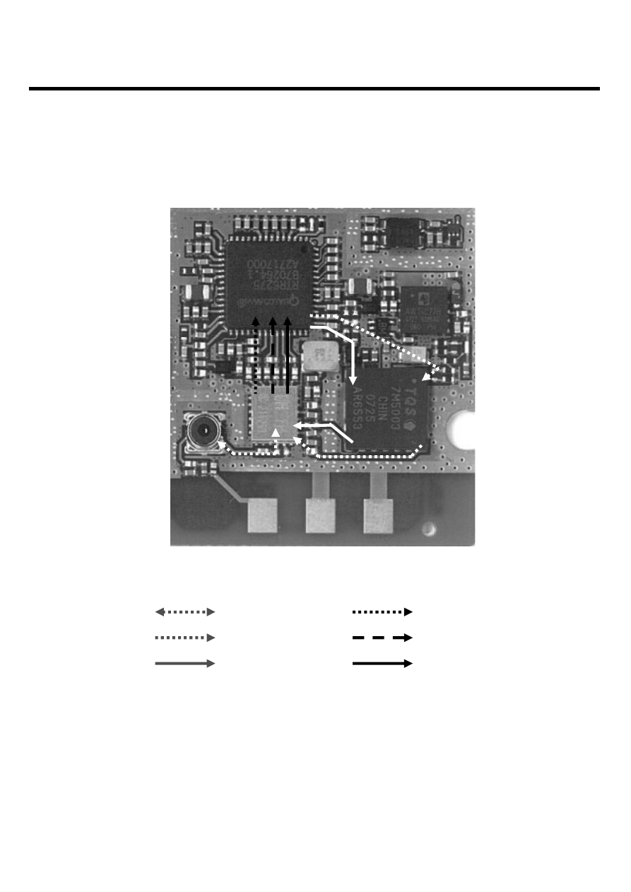
4.2.2 GSM PATH
- 95 -
4. TROUBLE SHOOTING
LGE Internal Use Only
Copyright © 2007 LG Electronics. Inc. All right reserved.
Only for training and service purposes
COMMON TX/RX PATH
DCS/PCS TX PATH
GSM TX PATH
GSM RX PATH
PCS RX PATH
DCS RX PATH
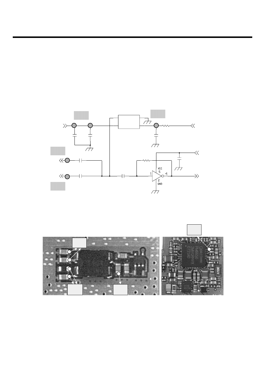
LGE Internal Use Only
Copyright © 2007 LG Electronics. Inc. All right reserved.
Only for training and service purposes
4.3 Checking VCTCXO Block
The reference frequency (19.2MHz) from X100 (VCXO) is used UMTS TX part, GSM part and BB part.
4. TROUBLE SHOOTING
- 96 -
TCXO
0.1u
C139
C147
1000p
100ohm
R115
1000p
C145
0.01u
C141
8200p
C148
1000p
C140
X100
2
GND
OUT
3
VCC
4
VCONT
1
19.2MHz
R120 100K
TC7SH04FS
U102
C144
1000p
TRK_LO_ADJ
VREG_TCXO_2.85V
TCXO_BT
VREG_BT_2.85V
TCXO_PM
RTR6275_TCXO
TP1
TP2
TP3
TP4
Schematic of the TCXO Block
Test Point of the TCXO Blcok
TP1
TP2
TP4
TP3
LGE Internal Use Only
Copyright © 2007 LG Electronics. Inc. All right reserved.
Only for training and service purposes
4. TROUBLE SHOOTING
- 97 -
Check TP1
VCC of VCXO
VCC ≥ 2.8V
Check TP2
TRK_LO_ADJ
3V≥ Voltage≥ 0V
Check TP3, TP4
With Oscilloscope
19.2MHz Signal
VCXO is OK
Check other part
Check PMIC
Check MSM
Check soldering
and components
Yes
Yes
Yes
No
No
No
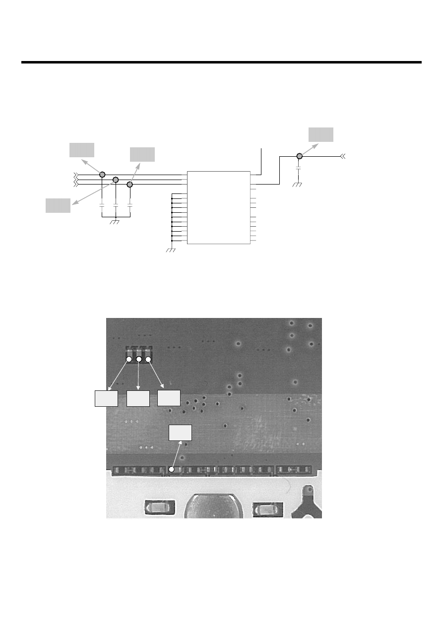
LGE Internal Use Only
Copyright © 2007 LG Electronics. Inc. All right reserved.
Only for training and service purposes
4.4 Checking Front-End Module Block
4. TROUBLE SHOOTING
- 98 -
Schematic of the Front-End Module Block
Test Point of Front-End Module Block
47p
C109
C115
47p
47p
C113
12
GND5
14
GND6
GND7
15
GND8
17
18
GND9
NC
7
PCS_RX1
22
PCS_RX2
21
25
PGND1
26
PGND2
8
UMTS_TX_RX
VC1
5
4
VC2
VC3
3
VDD
6
ANT
10
DCS_PCS_TX
13
DCS_RX1
20
19
DCS_RX2
EGSM_RX1
24
23
EGSM_RX2
EGSM_TX
16
1
GND1
2
GND2
GND3
9
11
GND4
LSHS-M090UH
47p
C114
VREG_RF_SMPS
ANT_SEL2
ANT_SEL0
ANT_SEL1
TP1
TP2
TP3
TP4
TP1
TP3
TP4
TP2
LGE Internal Use Only
Copyright © 2007 LG Electronics. Inc. All right reserved.
Only for training and service purposes
4. TROUBLE SHOOTING
- 99 -
- UMTS Tx/Rx
- GSM900 Tx
- DCS1800/PCS1900 Tx
- GSM Rx / PCS1900 Rx
Logic Table of the FEM
Vc3
Vc2
Vc1
Vdd
GSM900 Tx
L
H
H
H
DCS1800/PCS1900 Tx
L
L
H
H
UMTS Tx/Rx
H
L
H
H
GSM 900 Rx
L
L/H
L
H
DCS 1800 Rx
H
L/H
L
H
PCS 1900 Rx
L
L/H
L
H
TP2 (Vc2)
TP3 (Vc3)
TP1 (Vc1)
TP2 (Vc2)
TP3 (Vc3)
TP1 (Vc1)
TP2 (Vc2)
TP3 (Vc3)
TP1 (Vc1)
TP2 (Vc2)
TP3 (Vc3)
TP1 (Vc1)
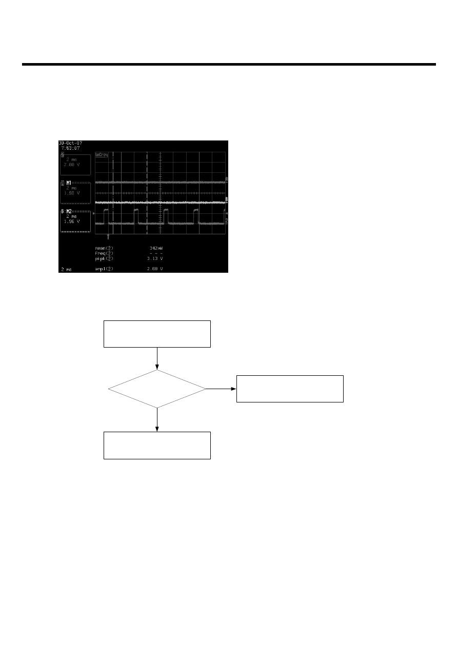
- 100 -
4. TROUBLE SHOOTING
- DCS1800 Rx
Checking Switch Block power source
LGE Internal Use Only
Copyright © 2007 LG Electronics. Inc. All right reserved.
Only for training and service purposes
Check Soldering
ANT_SEL0, 1, 2 High Level
2.5V < Voltgae < 3.0V
Check VDD
TP4 VREG_RF_SMPS
Check the Logic
in each mode
YES
NO
TP2 (Vc2)
TP3 (Vc3)
TP1 (Vc1)
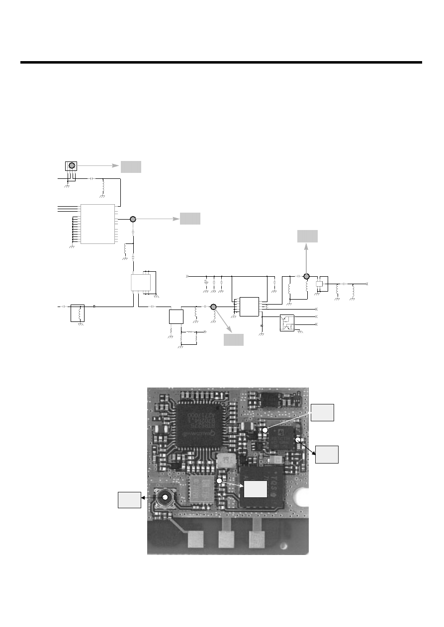
- 101 -
4. TROUBLE SHOOTING
LGE Internal Use Only
Copyright © 2007 LG Electronics. Inc. All right reserved.
Only for training and service purposes
4.5 Checking UMTS Block
4.5.1 Checking TX level
Schematic of the WCDMA Tx Block
Test Point of the WCDMA Tx Block
NA
L102
A
C
G1
G2
KMS-518
SW100
120p
C101
12
GND5
14
GND6
GND7
15
GND8
17
18
GND9
NC
7
PCS_RX1
22
PCS_RX2
21
25
PGND1
26
PGND2
8
UMTS_TX_RX
VC1
5
4
VC2
VC3
3
VDD
6
ANT
10
DCS_PCS_TX
13
DCS_RX1
20
19
DCS_RX2
EGSM_RX1
24
23
EGSM_RX2
EGSM_TX
16
1
GND1
2
GND2
GND3
9
11
GND4
FL100
LSHS-M090UH
PQ
20dB
8 dB
NA
C165
L125
1.2nH
100p
C163
L121
2.2nH
C160
22u
51
R124
L122
NA
100
R126
C168
2
4
5
3
1
56p
Q100
KRX102E
C162
0.01u
15nH
L123
2
RFIN
RFOUT
8
VCC1
1
10
VCC2
4
VMODE
VREF
5
AWT6277R
U105
GND1
3
GND2
6
7
GND3
9
GND4
GND5
11
C167
56p
5.6p
C169
C161
56p
SCDY0003403
50OHM
4
3
COUP
2
IN
1
OUT
C173
100p
U104
R123
68
C159
8.2p
C152
3.9p
1.8p
C170
L128
4.7nH
L124
3.3nH
L126
8.2nH
EFCH1950TDF1
FL104
G1
2
G2
3
G3
5
IN
1
O1
4
R125
100
1u
C164
C156
2.2p
FL103
ANT
2
1
GND1
GND2
4
8
GND3
GND4
9
GND5
6
GND6
3
7
RX
5
TX
SAYZY1G95EB0B00
WCDMA_2100_TX_OUT
PA_ON
VREG_TCXO_2.85V
+VPWR
PA_R1
PWR_DET
TP1
TP2
TP3
TP4
TP1
TP2
TP3
TP4
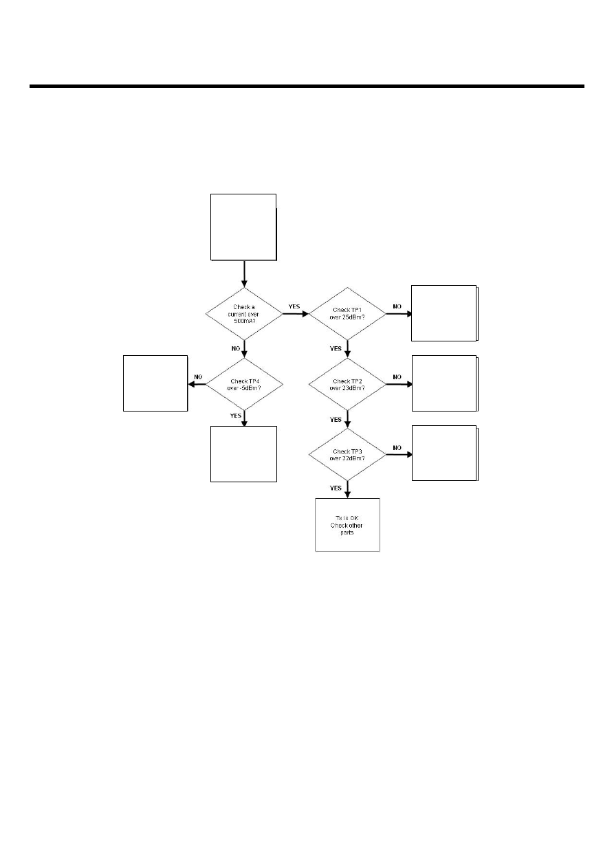
LGE Internal Use Only
Copyright © 2007 LG Electronics. Inc. All right reserved.
Only for training and service purposes
4. TROUBLE SHOOTING
- 102 -
For testing, Max power of UMT 2100 is needed.
Run a FTM program
set RF mode to IMT
set uplink freq. To
9750 click Tx on and
WCDMA set PA range
R1 on set Tx AGC to
410
Check Tx SAW
Filter
FL104
Check PAM block
U105
Check coupler U104
Check Duplexer
FL103
Check FEM FL100
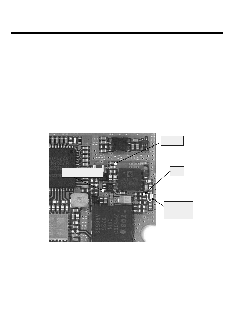
LGE Internal Use Only
Copyright © 2007 LG Electronics. Inc. All right reserved.
Only for training and service purposes
4. TROUBLE SHOOTING
- 103 -
4.5.2 Checking UMTS PAM Control Block
• PAM control signal
1. PWR_DET : UMTS Tx Power Detected value (Check R123)
2. TX_AGC_ADJ : UMTS RTR6275 Tx Amp Gain Control
3. VREG_TCXO_2.85V : UMTS PAM enable (about 2.85V)
4. +VPWR : UMTS PAM Main Voltage ( 3V < +VPWR < 4.2V)
5. PA_ON : Turns the PA on and off
6. PA_R1 : Control signals that step the active PA mode and bias
+VPWR
VREG_TCXO_2.85V
R123
UMTS2100
Coupler
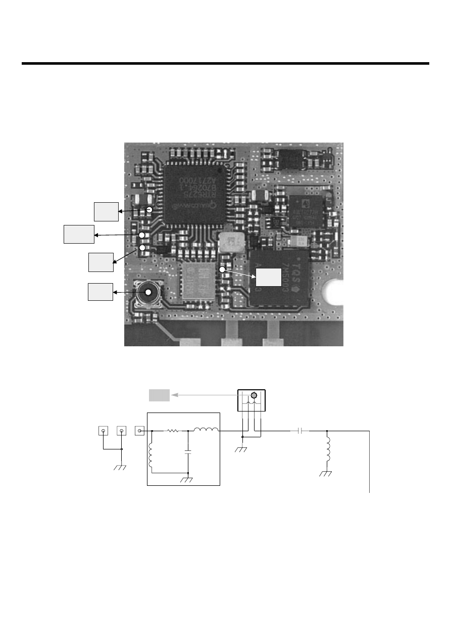
- 104 -
4. TROUBLE SHOOTING
4.5.3 Checking RX level
LGE Internal Use Only
Copyright © 2007 LG Electronics. Inc. All right reserved.
Only for training and service purposes
TP1
TP2
TP3
TP4
Vbias
PQ
C104
1.2p
ANT101
NA
L102
A
C
G1
G2
KMS-518
SW100
120p
C101
FL100
ANT100
0
L100
C102
12nH
L101
4.7nH
ANT102
TP1
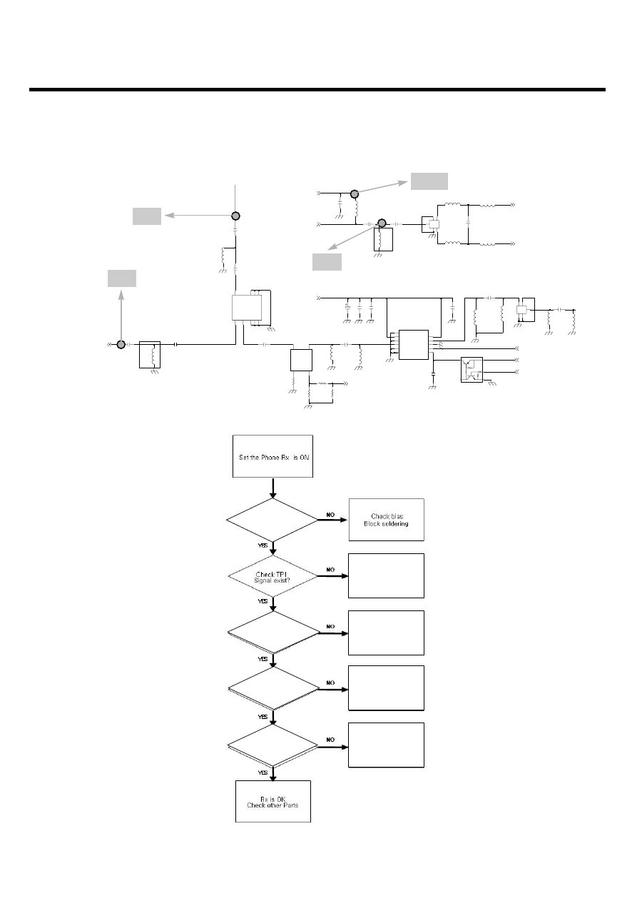
- 105 -
4. TROUBLE SHOOTING
LGE Internal Use Only
Copyright © 2007 LG Electronics. Inc. All right reserved.
Only for training and service purposes
PQ
PQ
20dB
8 dB
NA
C165
L125
1.2nH
1nH
L118
C149
22p
1.5nH
L114
100p
C163
L121
2.2nH
C160
22u
51
R124
100
R126
C168
2
4
5
3
1
56p
Q100
KRX102E
C162
0.01u
15nH
L123
C153
56p
2
RFIN
RFOUT
8
VCC1
1
10
VCC2
4
VMODE
VREF
5
AWT6277R
U105
GND1
3
GND2
6
7
GND3
9
GND4
GND5
11
C167
56p
5.6p
C169
L119
1nH
C161
56p
SCDY0003403
50OHM
4
3
COUP
2
IN
1
OUT
C173
100p
U104
R123
68
0.5p
C155
C159
8.2p
C154
56p
C152
3.9p
1.8p
C170
L116
1nH
L128
4.7nH
L124
3.3nH
L126
8.2nH
FL102
EFCH2140TDE1
G1
2
G2
5
IN
1
O1
3
O2
4
EFCH1950TDF1
FL104
G1
2
G2
3
G3
5
IN
1
O1
4
R125
100
L117
1.8nH
L115
1nH
1u
C164
C156
2.2p
FL103
ANT
2
1
GND1
GND2
4
8
GND3
GND4
9
GND5
6
GND6
3
7
RX
5
TX
SAYZY1G95EB0B00
PA_ON
VREG_TCXO_2.85V
+VPWR
PA_R1
WLNA_OUT
WCDMA_MIX_IN_M
WCDMA_MIX_IN_P
VDD_RX
RX_WCDMA_2100
PWR_DET
Check Vbias over 2V?
Check the RF S/W
Check FEM
FL100
Check the Duplexer
FL103
Check the RTR6275
U100
Check TP2
Signal exist?
Check TP3
Signal exist?
Check TP4
Signal exist?
TP2
Vbias
TP4
TP3
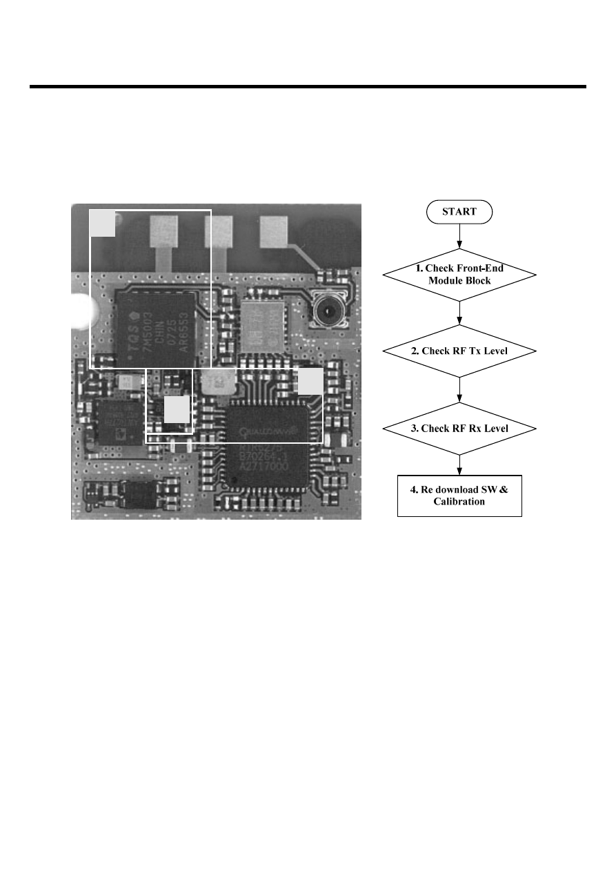
- 106 -
4. TROUBLE SHOOTING
4.6 Checking GSM Block
4.6.1 Checking Front-End Module
Refer to chapter 3.4
LGE Internal Use Only
Copyright © 2007 LG Electronics. Inc. All right reserved.
Only for training and service purposes
1
2
3
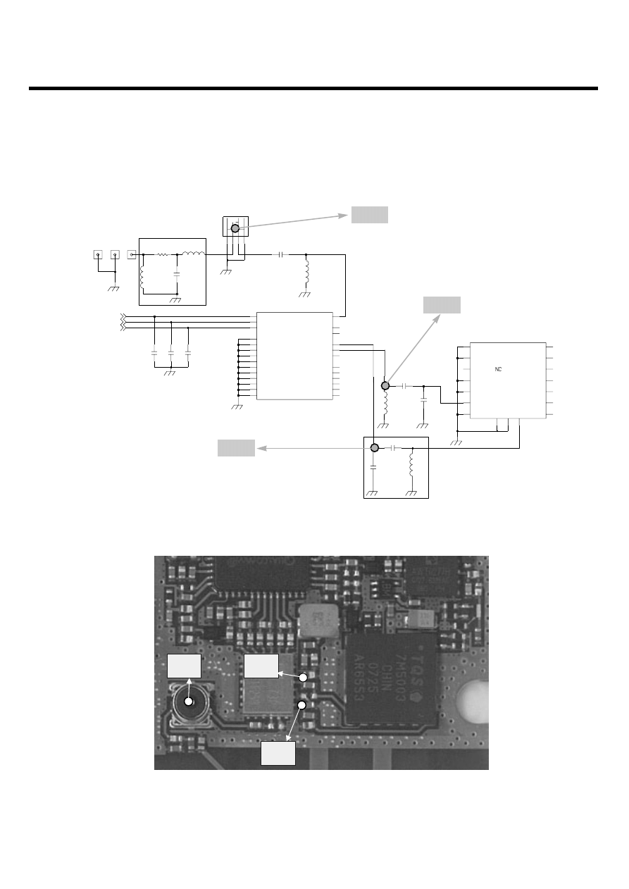
- 107 -
4. TROUBLE SHOOTING
LGE Internal Use Only
Copyright © 2007 LG Electronics. Inc. All right reserved.
Only for training and service purposes
4.6.2 Checking RF Tx Level
PQ
C104
1.2p
ANT101
C115
47p
47p
C113
NA
L102
A
C
G1
G2
KMS-518
SW100
120p
C101
12
GND5
14
GND6
GND7
15
GND8
17
18
GND9
NC
7
PCS_RX1
22
PCS_RX2
21
25
PGND1
26
PGND2
8
UMTS_TX_RX
VC1
5
4
VC2
VC3
3
VDD
6
ANT
10
DCS_PCS_TX
13
DCS_RX1
20
19
DCS_RX2
EGSM_RX1
24
23
EGSM_RX2
EGSM_TX
16
1
GND1
2
GND2
GND3
9
11
GND4
FL100
LSHS-M090UH
47p
C114
ANT100
0
L100
C102
12nH
L101
4.7nH
ANT102
ANT_SEL2
ANT_SEL0
ANT_SEL1
PQ
C138
NA
C142
0.75p
8p
C136
L113
14
GND6
GND7
16
17
GND8
7
GSM_IN
9
GSM_OUT
3
TX_EN
VBATT
4
12
VCC
VRAMP
6
4.7nH
TQM7M5003
U101
2
BS
DCS_PCS_IN
1
DCS_PCS_OUT
15
5
GND1
GND2
8
10
GND3
11
GND4
13
GND5
15nH
L112
C146
10p
Schematic of the GSM Tx Block
Test Point of GSM Tx Block
TP1
TP2
TP3
TP1
TP2
TP3
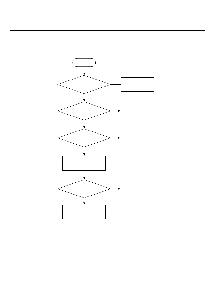
LGE Internal Use Only
Copyright © 2007 LG Electronics. Inc. All right reserved.
Only for training and service purposes
4. TROUBLE SHOOTING
- 108 -
START
Check TP1
If GSM over 31 dBm?
If DCS/PCS over 28dBm?
Check TP2, TP3
If TP2 over 29dBm?
If TP3 over 25dBm?
Check PAM Block OK?
Refer to chapter 3.6.3
Check Soldering of PAM (U101)
If problem still exist,
replace the PAM
Change the Board
Problem resolved ?
Yes
Yes
Yes
Yes
No
No
No
No
GSM/DCS/PCS Tx is OK
Check other part
Check Front-End
Module
Refer to chapter 3.4
Check the RTR6275
GSM/DCS/PCS Tx is OK
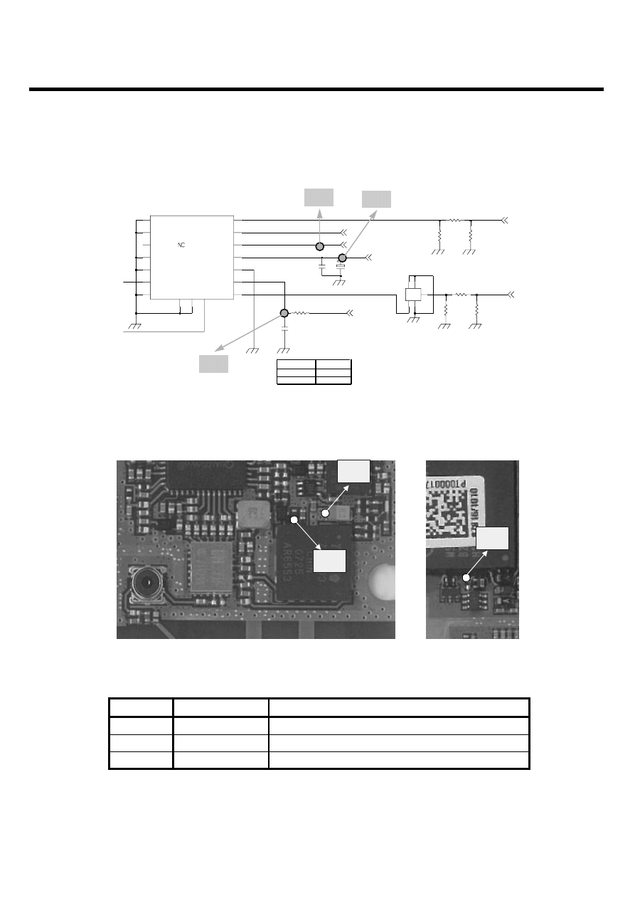
- 109 -
4. TROUBLE SHOOTING
LGE Internal Use Only
Copyright © 2007 LG Electronics. Inc. All right reserved.
Only for training and service purposes
4.6.3 Checking PAM Block
HIGH
MODE
LOW
GSM_PA_BAND
10 dB
GSM
DCS/PCS
8 dB
33u
C135
120
R119
120
R118
51
R114
91
R112
R117
2.2K
91
R113
1u
C137
14
GND6
GND7
16
17
GND8
7
GSM_IN
9
GSM_OUT
3
TX_EN
VBATT
4
12
VCC
VRAMP
6
TQM7M5003
U101
2
BS
DCS_PCS_IN
1
DCS_PCS_OUT
15
5
GND1
GND2
8
10
GND3
11
GND4
13
GND5
2
G1
3
G2
5
G3
1
IN
4
O1
EFCH897MTDB1
FL101
68p
C143
68
R111
GSM_PA_BAND
+VPWR
DCS_PCS_TX
GSM_TX
GSM_PA_RAMP
GSM_PA_EN
TP1
TP2
TP3
Test Point
Net name
Description
TP1 GSM_PA_RAMP
Power Amp Gain Control. Typically, 0.2 ~1.6V
TP2 GSM_PA_EN
Power Amp Enable (ON : >2.5V, OFF : <0.7V)
TP3
+VPWR
PAM Supply Voltage (Vcc > 3V)
Schematic of PAM Block
Test Point of PAM Block
TP1
TP2
TP3
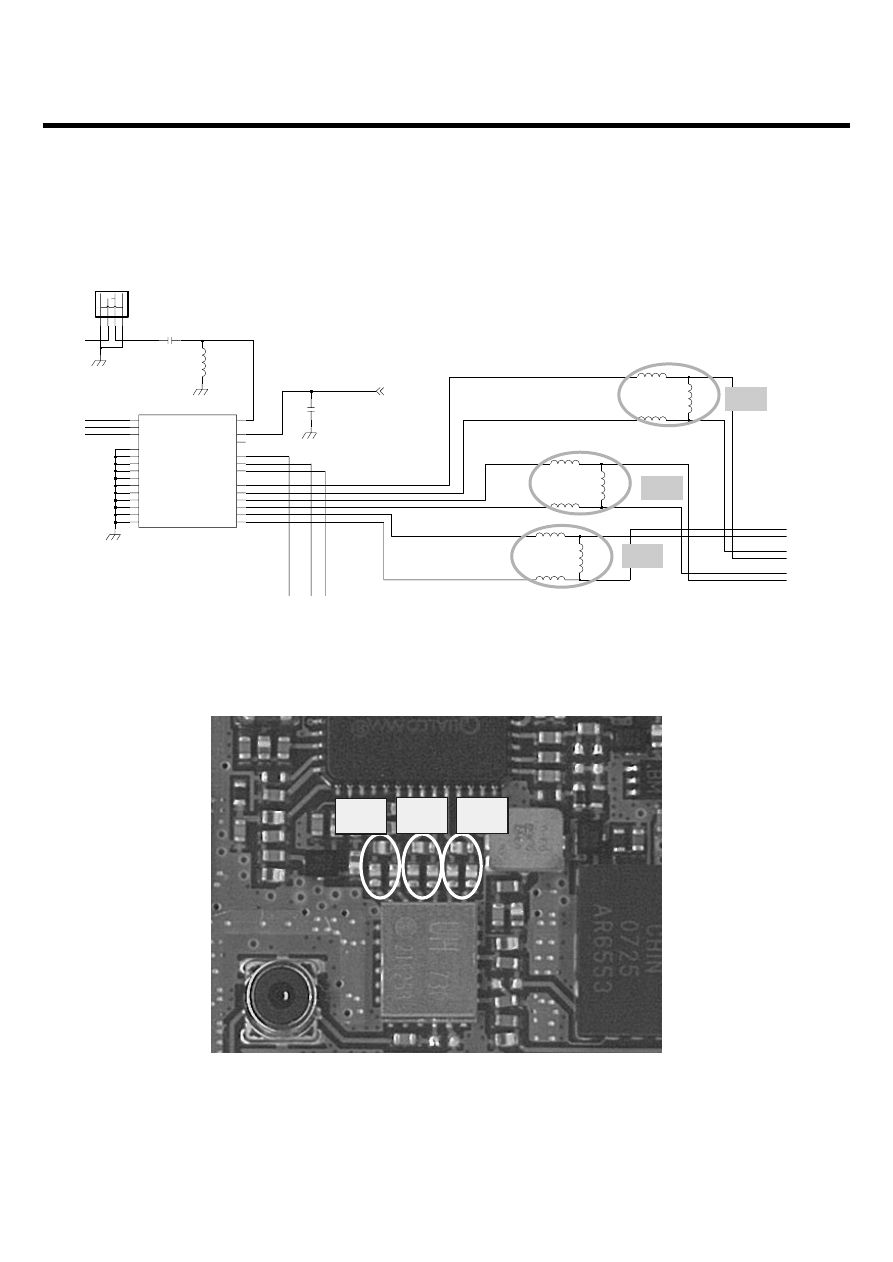
- 110 -
4. TROUBLE SHOOTING
4.6.4 Checking RF Rx Level
LGE Internal Use Only
Copyright © 2007 LG Electronics. Inc. All right reserved.
Only for training and service purposes
Schematic of GSM-900, DCS-1800, PCS-1900 Rx Block
Test Point of Rx Block
DCS
GSM
PCS
15nH
L104
47p
C109
5.6nH
L103
15nH
L107
NA
L102
A
C
G1
G2
KMS-518
SW100
L109
22nH
120p
C101
12
GND5
14
GND6
GND7
15
GND8
17
18
GND9
NC
7
PCS_RX1
22
PCS_RX2
21
25
PGND1
26
PGND2
8
UMTS_TX_RX
VC1
5
4
VC2
VC3
3
VDD
6
ANT
10
DCS_PCS_TX
13
DCS_RX1
20
19
DCS_RX2
EGSM_RX1
24
23
EGSM_RX2
EGSM_TX
16
1
GND1
2
GND2
GND3
9
11
GND4
FL100
LSHS-M090UH
5.6nH
L105
5.6nH
L106
22nH
L110
L111
22nH
L108
5.6nH
VREG_RF_SMPS
TP1
TP2
TP3
TP3
TP2
TP1
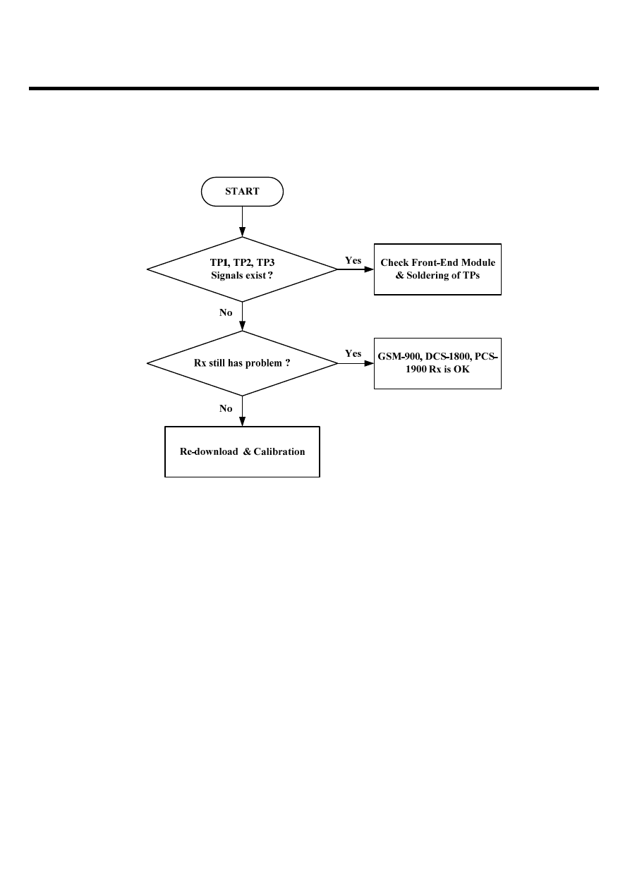
- 111 -
4. TROUBLE SHOOTING
LGE Internal Use Only
Copyright © 2007 LG Electronics. Inc. All right reserved.
Only for training and service purposes
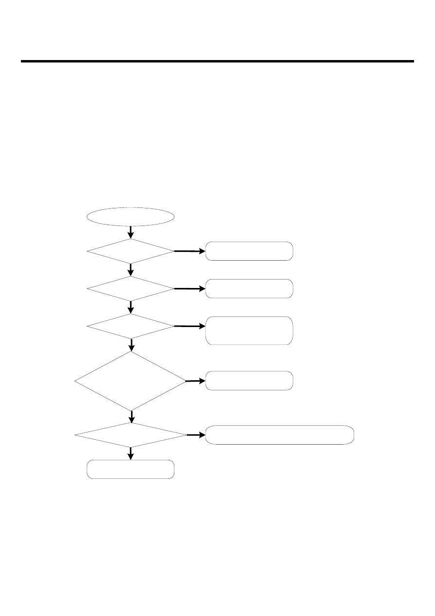
LGE Internal Use Only
Copyright © 2007 LG Electronics. Inc. All right reserved.
Only for training and service purposes
4. TROUBLE SHOOTING
- 112 -
4.7 Power on trouble
Power on sequence of KU990 is :
PWR key press
→ PM_ON_SW_N go to low (VA700, PM6650-2M KPDPWR_N pin#24) → PM6650-
2M Power Up
→ VREG_MSMC_1.2V(C560), VREG_MSME_1.8V(R520), VREG_MSMP_2.7V(R513),
VREG_MSMA_2.6V(R508), VREG_TCXO_2.85V(C510) power up
→ PON_RESET_N assert to MSM
→ Phone booting & PS_HOLD(D500) assert High to PMIC(PM6650-2M)
Start
Battery voltg. higher
than 3.2V?
Press PWR key
Keypad LED on?
VA700 high to low
when key press?
VREG_MSMC_1.2V,
VREG_MSMP_2.7V, VREG_MSME_1.8V
VREG_TCXO_2.85V,
VREG_MSMA_2.6V power up?
Is clock ok?
X100 : 19.2M
X500 : 32.768Khz
Change the Main board
Change or charging the
Battery
Follow the LED trouble
shoot
Check open Pattern
of power button
Check Dome Sheet
Change the Main board
Check the TXCO and SLEEP CRYSTAL
NO
YES
YES
YES
YES
YES
NO
NO
NO
NO
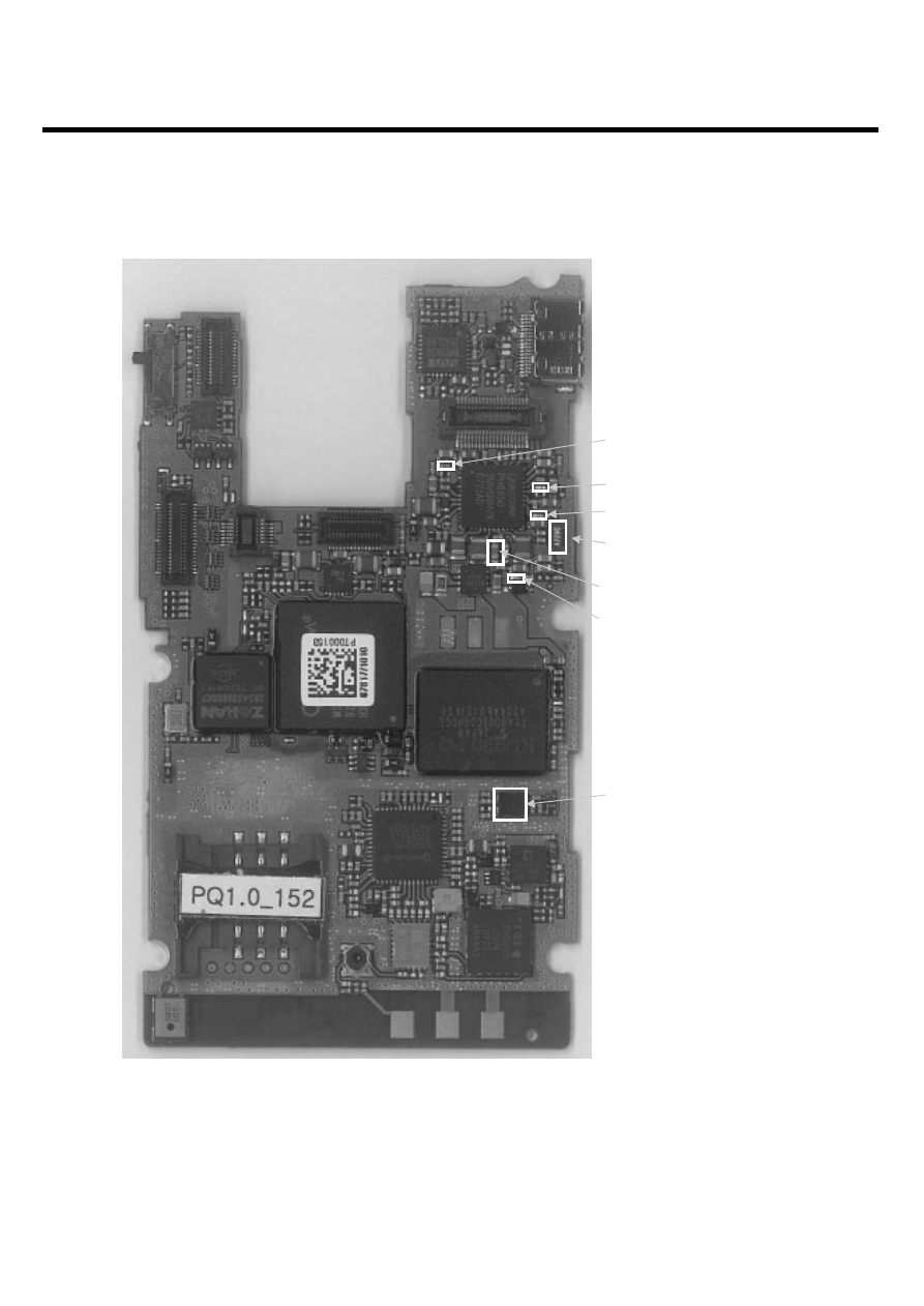
LGE Internal Use Only
Copyright © 2007 LG Electronics. Inc. All right reserved.
Only for training and service purposes
4. TROUBLE SHOOTING
- 113 -
VREG_MSMC_1.2V(C560)
VREG_MSME_1.8V(R520)
TCXO ( 19.2MHz )
VREG_MSMP_2.7V(R513)
VREG_MSMA_2.6V(R508)
VREG_TCXO_2.75V(C510)
SLEEP CRYSTAL(32.768KHz)
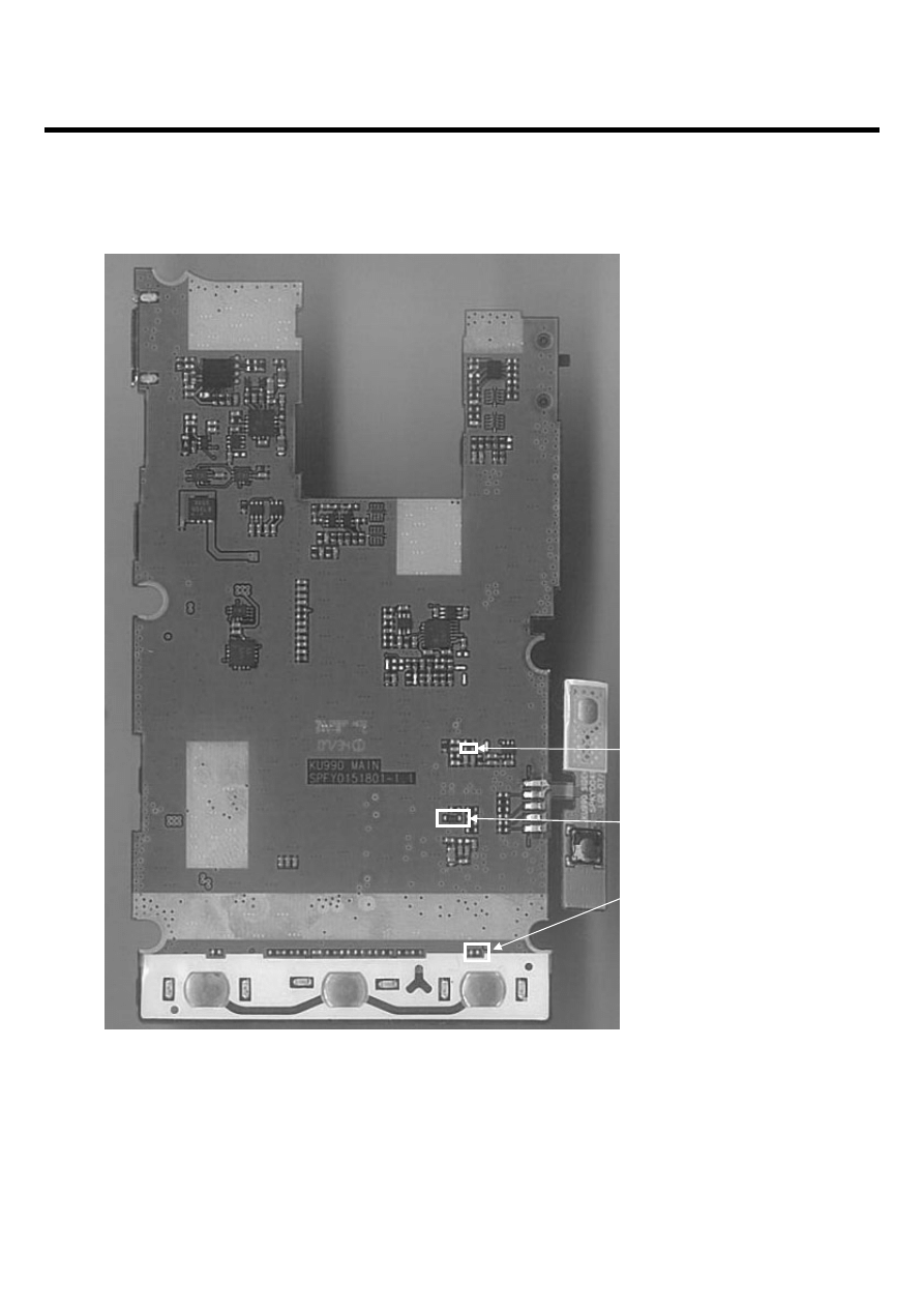
LGE Internal Use Only
Copyright © 2007 LG Electronics. Inc. All right reserved.
Only for training and service purposes
4. TROUBLE SHOOTING
- 114 -
PM_ON_SW_N (D700)
RESET_IN_N(R208)
PS_HOLD(D500)
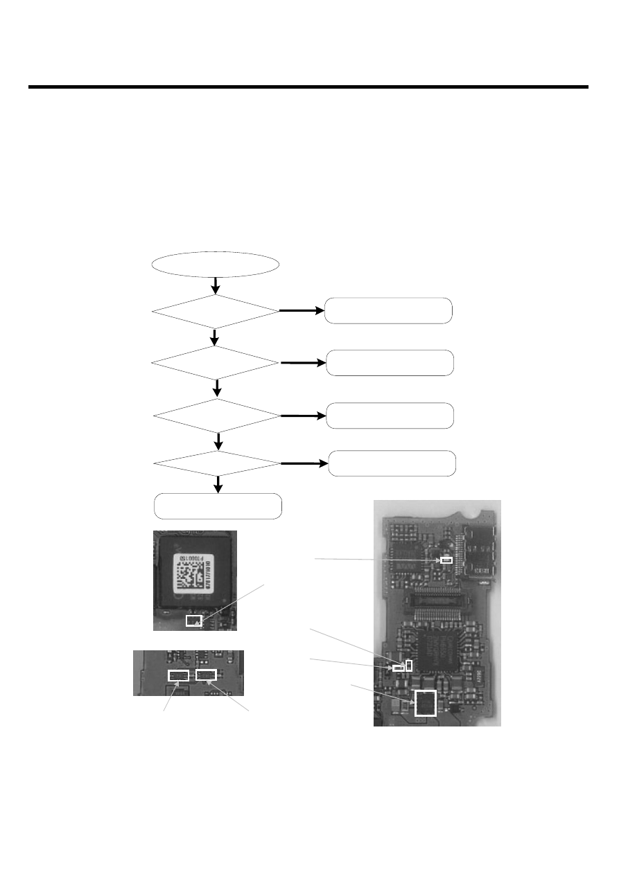
LGE Internal Use Only
Copyright © 2007 LG Electronics. Inc. All right reserved.
Only for training and service purposes
4. TROUBLE SHOOTING
- 115 -
4.7.1 USB trouble
USB Initial sequence of KU990 is :
USB connected to KU990
→ USB_VBUS(C540) go to 5V
→ USB_D+(VA202) go to 3.3V → 48M Crystal on → USB_DATA is triggered → USB work
Start
USB_VBUS is about
to 5V?
USB_D+ is about to 3.3V?
48MHz is run?
Change the Main board
Check C540, R514,U500
USB cable
Check VA500,U507,U304
Check X200
NO
YES
YES
YES
NO
NO
Cable is insert?
YES
Cable insert
NO
X200(48MHz)
C540(USB_VBUS)
U507(USB_D+)
R514(USB_VBUS)
U500(USB_VBUS)
VA500(USB_D+)
U304(USB_D+)
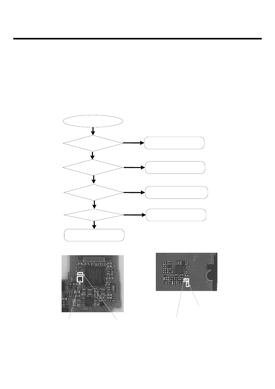
LGE Internal Use Only
Copyright © 2007 LG Electronics. Inc. All right reserved.
Only for training and service purposes
4. TROUBLE SHOOTING
- 116 -
4.7.2 UMS(USB MASS STORAGE) trouble
UMS Initial sequence of KU990 is :
USB connected to KU990
→ VREG_5V(R335, UMS) go to 5V → VREG_USB_3.3V(R301) go to 3.3V
→ USB_DATA is triggered → USB work
Start
VREG_5V is about
to 5V?
VREG_USB_3.3V is
about to 3.3V?
MICRO SD function OK?
Change the Main board
Check R335, D501
Check R301,C529, USB CABLE
Follow the micro sd trouble
NO
YES
YES
YES
NO
NO
Cable is insert?
YES
Cable insert
NO
C529 (VREG_USB_3.3V)
D501(VREG_5V)
< TOP SIDE >
R335(VREG_5V)
R301(VREG_USB_3.3V)
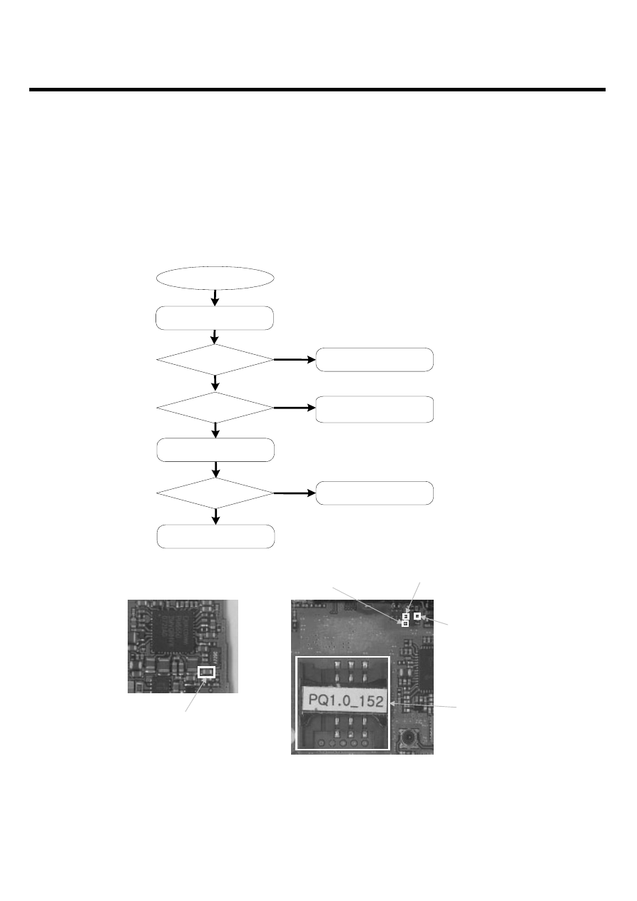
LGE Internal Use Only
Copyright © 2007 LG Electronics. Inc. All right reserved.
Only for training and service purposes
4. TROUBLE SHOOTING
- 117 -
4.8 SIM detect trouble
USB Initial sequence of KU990 is :
VREG_USIM_3.0V(C552 of PM6650) go to 3.0V
→ USIM clock, reset and data triggered → USIM IF
work (Schematic and place are refer to SIM technical brief)
Start
Work well?
VREG_USIM_3.0V is 3.0V?
USIM_P_CLK is run?
Change the Main board
End
Check J400, D400,C552
Yes
No
YES
NO
Re-insert the SIM card
Change SIM card
Work well?
End
Yes
No
USIM_P_RST_N
C552(VREG_USIM_3.0V)
J400
USIM_P_CLK
USIM_P_DATA
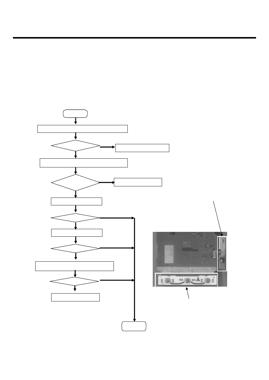
LGE Internal Use Only
Copyright © 2007 LG Electronics. Inc. All right reserved.
Only for training and service purposes
4. TROUBLE SHOOTING
- 118 -
4.9 Key sense trouble ( KEYPAD )
Key Sense sequence of KU990 is :
Default condition ROW(0-2) is 2.7V
→ Press the key → Corresponding ROW(x) and COL(x) go to 0V
→ Scan pulse( Col => Row ) → MSM sense what key pressed.
Check the R701,R705,R706 with no key press
Change the Main board
Yes
NO
Change the DOME SHEET
Check the R701,R705,R706 with key press
ROW(0-2) is 2.7V?
Check
R701,R705,R706
NO
Yes
ROW(0-2),
COL(0-1) is 0V?
Work well?
End
START
Check VA700~ VA707, R707~R710
NO
YES
NO
Change SIDE KEY
Work well?
NO
Work well?
YES
YES
NO
Dome sheet
Side Key
Change the Main board
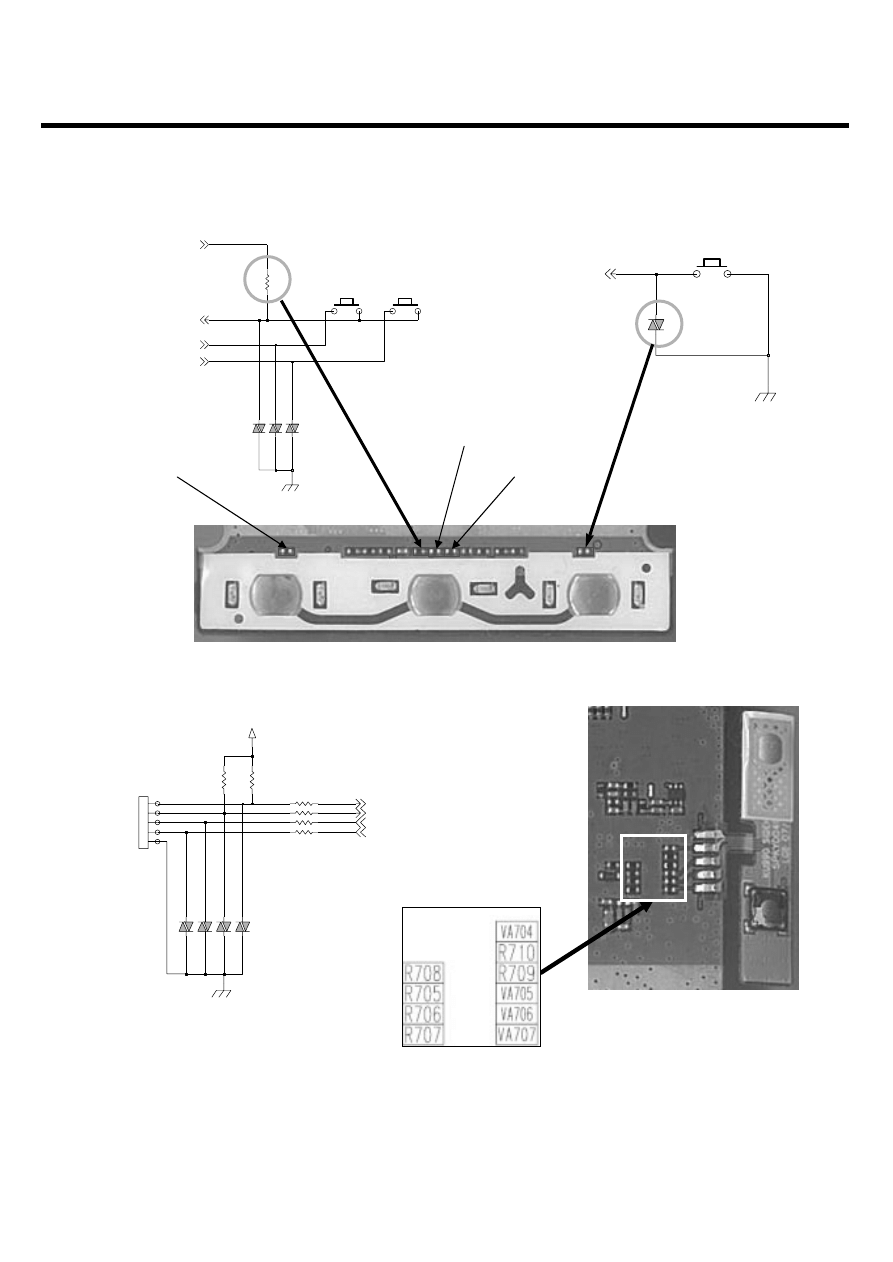
LGE Internal Use Only
Copyright © 2007 LG Electronics. Inc. All right reserved.
Only for training and service purposes
4. TROUBLE SHOOTING
- 119 -
Schematic of key sense part
CLR
SEND
R701
51K
701
700
VA702
EVLC14S02050
VA701
EVLC14S02050
EVLC14S02050
VA703
KEY_ROW[2]
VREG_MSMP_2.7V
KEY_COL[0]
KEY_COL[1]
END
ON_SW KEY
EVL14K02200
VA700
END
PM_ON_SW_N
VA702(COL0)
SEND
VA703(COL1)
VA701(ROW2)
CLR
END
SIDE KEY
470
R709
R710
470
470
R708
51K
R706
VA704
EVLC14S02050
51K
R705
VREG_MSMP_2.7V
R707
470
EVLC14S02050
VA707
EVLC14S02050
VA706
VA705
EVLC14S02050
5
CN700
1
2
3
4
KEY_ROW[0]
KEY_ROW[1]
KEY_COL[1]
KEY_COL[0]
LOCK
SHOT
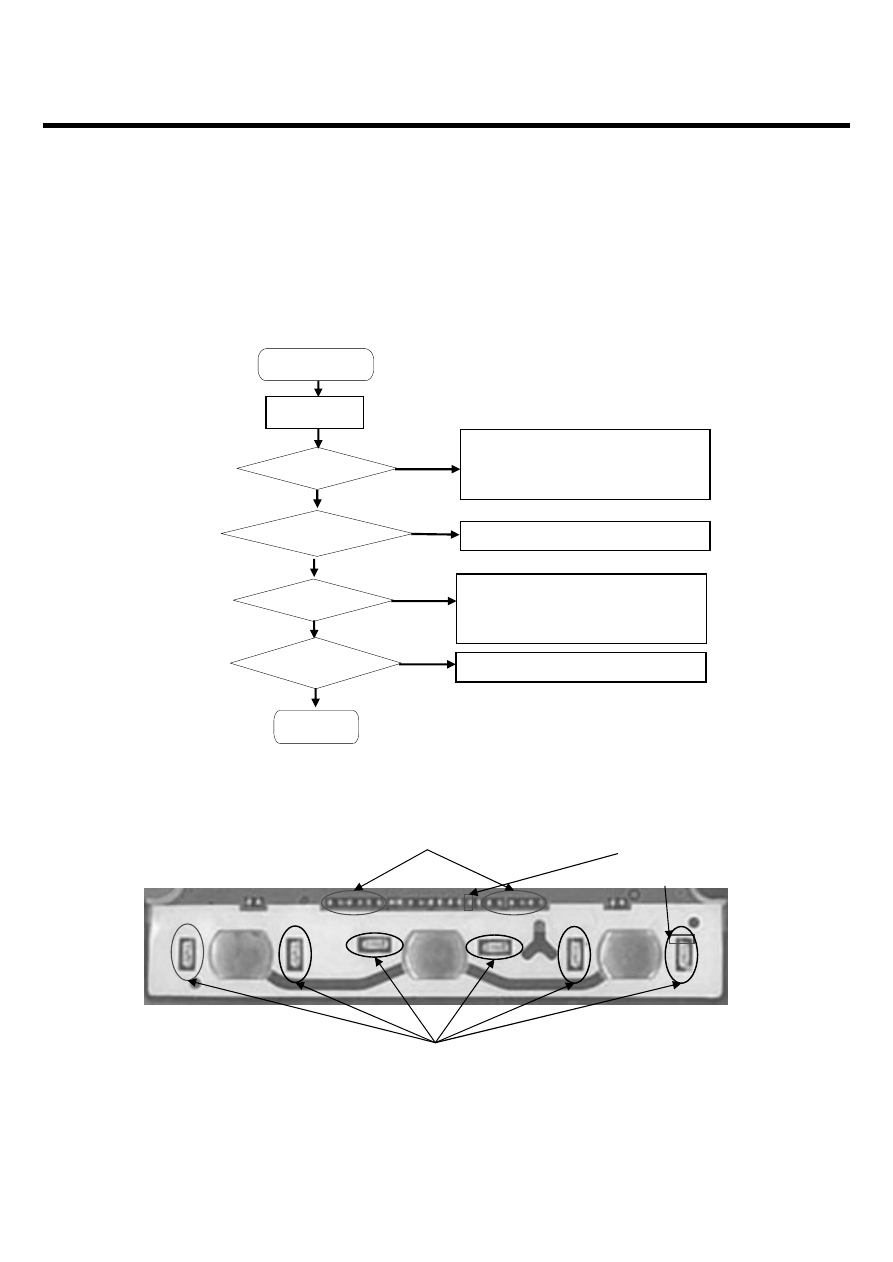
LGE Internal Use Only
Copyright © 2007 LG Electronics. Inc. All right reserved.
Only for training and service purposes
4. TROUBLE SHOOTING
- 120 -
4.10 Keypad backlight trouble
Key Pad Back Light is on as below :
Key pressing
→ PM6650 KYPD_LED_EN go to Low → LED On (Key Pad LED controlled by PM6650)
Start
Check device short :
LD700~705 and R711~716 (Main)
NO
Yes
Key press
Signal KYPD_LED_EN
is Low?
+VPWR is OK?
Change the main board
NO
Yes
Yes
Check device open :
LD700~705 and R711~716 (Main)
NO
Some LED
is not work?
Work well?
Yes
Change the main board
NO
End
LD700~705 (Main)
LD703 (+VPWR)
VA708 (KYPD_LED_EN)
R711~716 (Main)
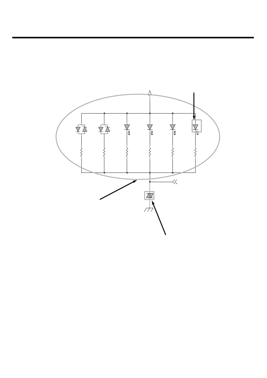
LGE Internal Use Only
Copyright © 2007 LG Electronics. Inc. All right reserved.
Only for training and service purposes
4. TROUBLE SHOOTING
- 121 -
(GREEN)
Rev. 1.1
(WHITE)
(RED)
R711
47
LD701
SSC-FR104-II1
R712
200
SSC-FR104-II1
200
R714
LD703
EVL14K02200
VA708
SSC-TWH104-HL
LD704
R715
47
SSC-TWH104-HL
R713
47
LD700
LEGG-S14G
LD702
LD705
LEGG-S14G
47
R716
KYPD_LED_EN
+VPWR
LD700~705 and R711~716 (Main)
VA708 (KYPD_LED_N)
LD703 (+VPWR)
Schematic of keypad backlight part
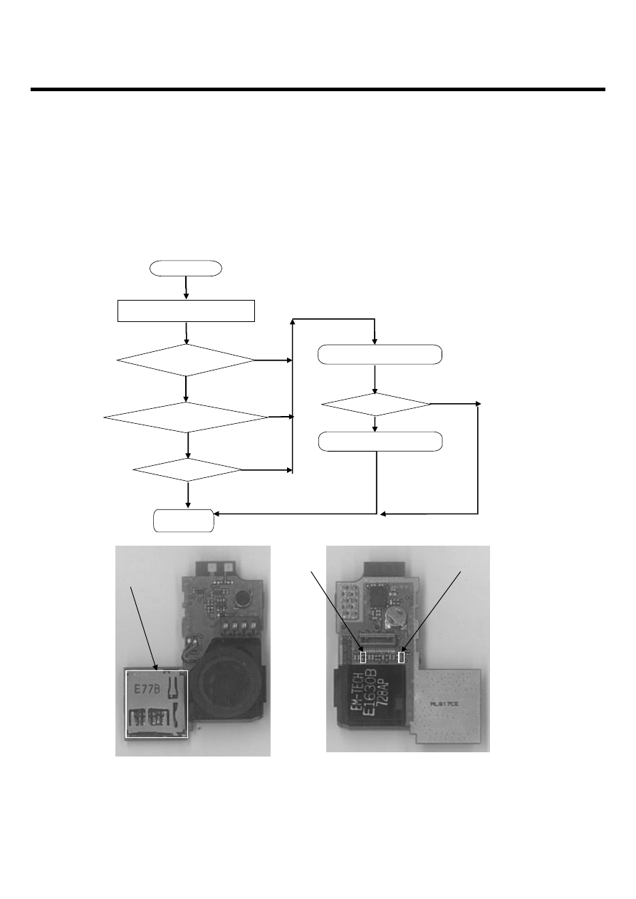
LGE Internal Use Only
Copyright © 2007 LG Electronics. Inc. All right reserved.
Only for training and service purposes
4. TROUBLE SHOOTING
- 122 -
4.11 Micro SD trouble
Micro SD is worked as below :
Micro SD insertion
→ MICROSD_DETECT(R804) goes to low → go working
MICROSD_DETECT(R804))
is low ?
Insert the Micro SD Card
Start
End
Check VREG_MMC_3.0V
is over 2.85V?
Work well?
YES
NO
SOCKET
R804(DETECT)
YES
Change the SUB board
Work well?
YES
NO
NO
Change the MAIN board
YES
NO
C807(VREG_MMC_3.0V)
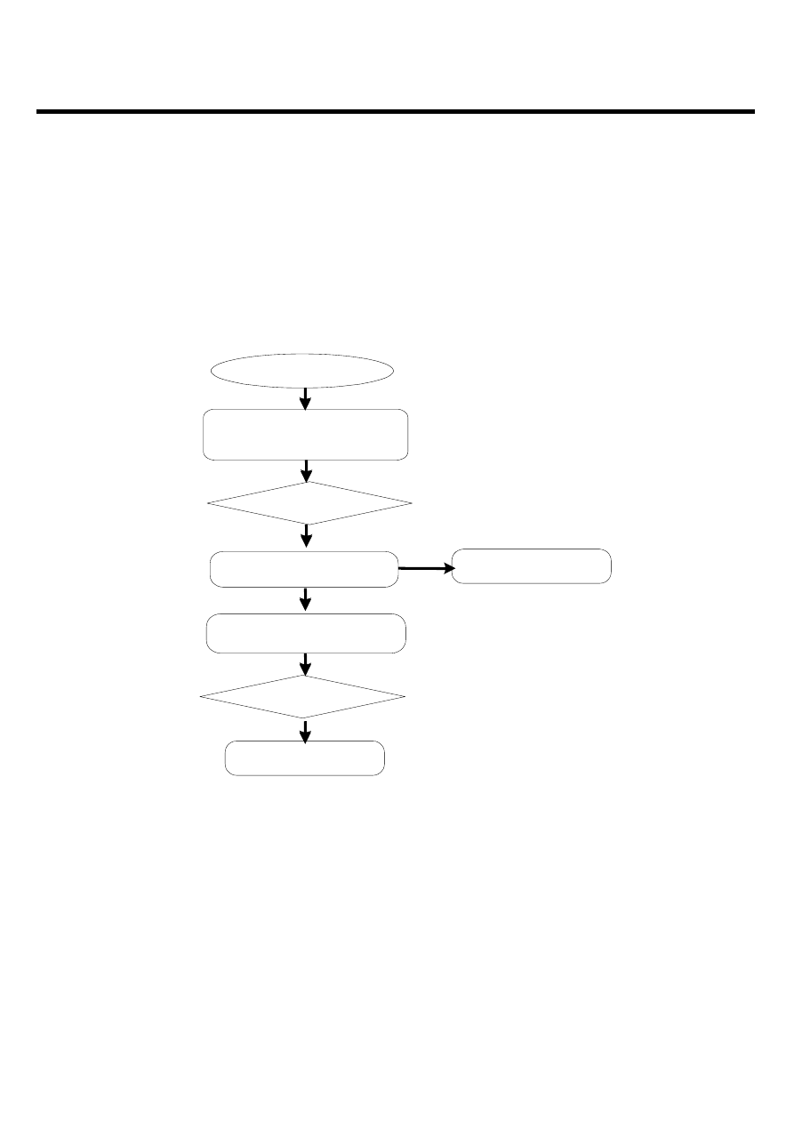
LGE Internal Use Only
Copyright © 2007 LG Electronics. Inc. All right reserved.
Only for training and service purposes
4. TROUBLE SHOOTING
- 123 -
4.12 Audio trouble
4.12.1 Receiver path
Voice Receiver path as below:
MSM6280 Ear1ON/Ear1OP
→ CN701(VGA CAM FPCB connector) → Receiver
Start
Connect the phone to network
Equipment and setup call
Setup 1KHz tone out
Can you hear the tone?
YES
END
Check connector pin
or change the VGA CAM FPCB
YES
Change the Receiver
Hear the tone to the receiver?
NO
END
LGE Internal Use Only
Copyright © 2007 LG Electronics. Inc. All right reserved.
Only for training and service purposes
4. TROUBLE SHOOTING
- 124 -
VGA CAM
FPCB
connector
Receiver
Receiver
pads
MSM6280

LGE Internal Use Only
Copyright © 2007 LG Electronics. Inc. All right reserved.
Only for training and service purposes
4. TROUBLE SHOOTING
- 125 -
4.12.2 Voice path for headset
Voice path for Head_Set as below:
MSM6280 HPH_R, HPH_L
→ C548,C549 U502(audio codec) → C578,C562 → R529,C522 →
U504(Headset AMP)
→ FB502, FB503 → R525, R524 → #4, #5 pin of CN500 headset Jack
Start
The sine wave appear at
C548,C549 ?
Change the Main board
NO
Connect the phone to network
Equipment and setup call
Setup 1KHz tone out
And insert head_Set
The sine wave appear at
C578,C562 ?
YES
Check the U502
or change the Main bíd
NO
Can you hear the tone?
NO
YES
YES
END
Headset insertion detection
in the Main LCD Display OK?
Check #8 pin of CN500
or change the Main bíd
NO
YES
Check the CN500 or change the
Main bíd
The sine wave appear at
R525,R524 ?
YES
Check the U504
or change the Main bíd
NO
LGE Internal Use Only
Copyright © 2007 LG Electronics. Inc. All right reserved.
Only for training and service purposes
4. TROUBLE SHOOTING
- 126 -
CN500
R524
R525
8
9
12
13
19
2
21
3
4
5
6
7
CN500
1
10
11
R528
100K
FB504
TV_OUT
EAR_MIC_P
RMT_PWR_ON_N
RMT_INT-USB_D+
RMT_ADC-USB_D-
VBATT
FM_ANT
MIDI_EAR_L
MIDI_EAR_R
EAR_SENSE_N
Schematic of voice path
LGE Internal Use Only
Copyright © 2007 LG Electronics. Inc. All right reserved.
Only for training and service purposes
4. TROUBLE SHOOTING
- 127 -
C548
C549
U502
FB501
FB500
NA
C550
0.1u
C514
C535
1u
C532
1u
R2_GPIO3
6
RIN
5
4
RIP
ROUT1
29
ROUT2
23
16
SCLK
SDIN
17
27
VMID
DACDAT
10
DBVDD
14
DCVDD
13
12
DGND
L2_GPIO2
3
LIN
2
1
LIP
LOUT1
30
25
LOUT2
7
LRC
11
MCLK
MICBIAS
32
18
MODE
OUT3
22
21
OUT4
33
PGND
U502
ADCDAT
9
28
AGND1
24
AGND2
AUXL
19
AUXR
20
31
AVDD1
AVDD2
26
8
BCLK
15
CSB_GPIO1
4.7u
C520
WM8983
C533
4.7n
R511
18K
R533
0
10u
C525
C534
1u
10u
C513
100K
R519
4.7n
C542
NA
C531
1K
R516
R510
1K
C541
1u
1u
C549
1u
C548
C536
1u
C518
4.7u
C539
1u
12n
C547
C524
0.1u
NA
C544
C519
0.1u
C551
NA
C521
0.1u
C543
NA
12n
C530
18K
R517
C516
4.7u
C517
0.1u
MIC_PWR
MMP_A_MCLK
CODEC_I2C_SCL
CODEC_I2C_SDA
HP_R
HP_L
HP_EAR_L
MIC2P
HP_EAR_R
MID_MICP
SPK_L
SPK_R
FM_AUDIO_L
FM_AUDIO_R
MMP_A_BCLK
MMP_ADO_DACDAT
MMP_A_LRCLK
MMP_ADI_ADCDAT
SPK_OUT-
SPK_OUT+
VREG_5V
VREG_WM_2.7V
VREG_MSME_1.8V
MIDI_3.3V
Schematic of voice path
U502
LGE Internal Use Only
Copyright © 2007 LG Electronics. Inc. All right reserved.
Only for training and service purposes
4. TROUBLE SHOOTING
- 128 -
Schematic of voice path
FB502
FB503
U504
C562
R522
C578
R529
PQ
PQ
R524
68
SVSS
16
_SHDN
C1N
4
2
C1P
INL+
15
INL_
14
7
INR+
INR_
8
OUTL
12
OUTR
10
3
PGND
PVDD
1
5
PVSS
P_G
17
SGND
6
13
SVDD1
9
SVDD2
11
U504
MAX9722BETE
4.7u
C565
C577
1u
R525
68
600
FB503
FB502
600
0.22u
C578
R522
15K
15K
R529
1u
C570
PRSB6.8C
C574
C573
PRSB6.8C
1u
C566
C562
0.22u
MIDI_EAR_R
MIDI_EAR_L
MIDI_3.3V
HP_AMP_EN
HP_EAR_L
HP_EAR_R
U504
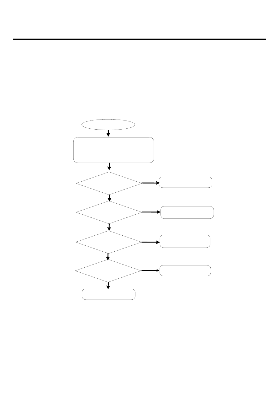
LGE Internal Use Only
Copyright © 2007 LG Electronics. Inc. All right reserved.
Only for training and service purposes
4. TROUBLE SHOOTING
- 129 -
4.12.3 Loud speaker path (voice speaker phone/VT)
Loud speaker path as below:
MSM6280 SPK_R, SPK_L
→ C532,C541 → R510,R516 → C533,C542 → R511,R517 →
U502(audio codec)
→ FB500,FB501 → CN603(B’toB connector) → OUT800, OUT801 (SPK PAD) →
Speaker
Start
The sine wave appear at
C532,C541?
Change the Main board
NO
Connect the phone to network
Equipment and setup call
Setup 1KHz tone out
Set phone with speaker phone mode
The sine wave appear at
FB500, FB501?
YES
Check the U502 or
Change the Main board
NO
Check the CN603
NO
YES
YES
Can you hear the tone?
Change the speaker
NO
YES
END
The sine wave appear at
pads of speaker?
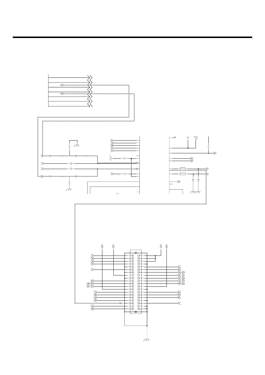
LGE Internal Use Only
Copyright © 2007 LG Electronics. Inc. All right reserved.
Only for training and service purposes
4. TROUBLE SHOOTING
- 130 -
MICBIAS
T15
AC18
LINE_ON
LINE_OP
AC17
HPH_L
W17
AA17
HPH_R
EAR1ON
AE18
EAR1OP
AF18
HP_R
HP_L
RCV+
RCV-
MICBIAS
SPK_L
SPK_R
FB501
FB500
C535
1u
C532
1u
R2_GPIO3
6
RIN
5
4
RIP
ROUT1
29
ROUT2
23
16
SCLK
27
VMID
DACDAT
10
L2_GPIO2
3
LIN
2
1
LIP
LOUT1
30
25
LOUT2
7
LRC
11
MCLK
MICBIAS
32
18
MODE
OUT3
22
21
OUT4
ADCDAT
9
24
AGND2
AUXL
19
AUXR
20
8
BCLK
15
CSB_GPIO1
C533
4.7n
R511
18K
10u
C525
C534
1u
K
9
4.7n
C542
NA
C531
1K
R516
R510
1K
C541
1u
C536
1u
C539
1u
12n
C547
C524
0.1u
NA
C544
C543
NA
12n
C530
18K
R517
MIC_PWR
MMP_A_MCLK
CODEC I2C SCL
HP_EAR_L
MIC2P
HP_EAR_R
MID_MICP
SPK_L
SPK_R
FM_AUDIO_L
FM_AUDIO_R
MMP_A_BCLK
MMP_ADO_DACDAT
MMP_A_LRCLK
MMP_ADI_ADCDAT
SPK_OUT-
SPK_OUT+
AXK740327G
VREG_MMC_3.0V
8
9
3
30
31
32
33
34
35
36
37
38
39
4
40
5
6
7
15
16
17
18
19
2
20
21
22
23
24
25
26
27
28
29
CN603
G1
G2
1
10
11
12
13
14
VREG_MSMP_2.7V
+VPWR
VREG_BT_2.85V
MMP_CAM_PWR_EN
SPK_OUT+
SPK_OUT-
HOOK_SENSE_N
EAR_MIC_P
MICROSD_DATA[1]
MICROSD_DETECT
MICROSD_CLK
MICROSD_DATA[0]
MICROSD_CMD
CAM_VDD_AF_2.7V
CAM_MIC+
WHEEL_SW_L
WHEEL_SW_R
CAM_VDD_SD_1.8V
V_BACK_UP
TCXO_BT
BT_TX_RX_N
BT_SBST
BT_SBCK
BT_SBDT
BT_CLK
BT_DATA
MICROSD_DATA[3]
MICROSD_DATA[2]
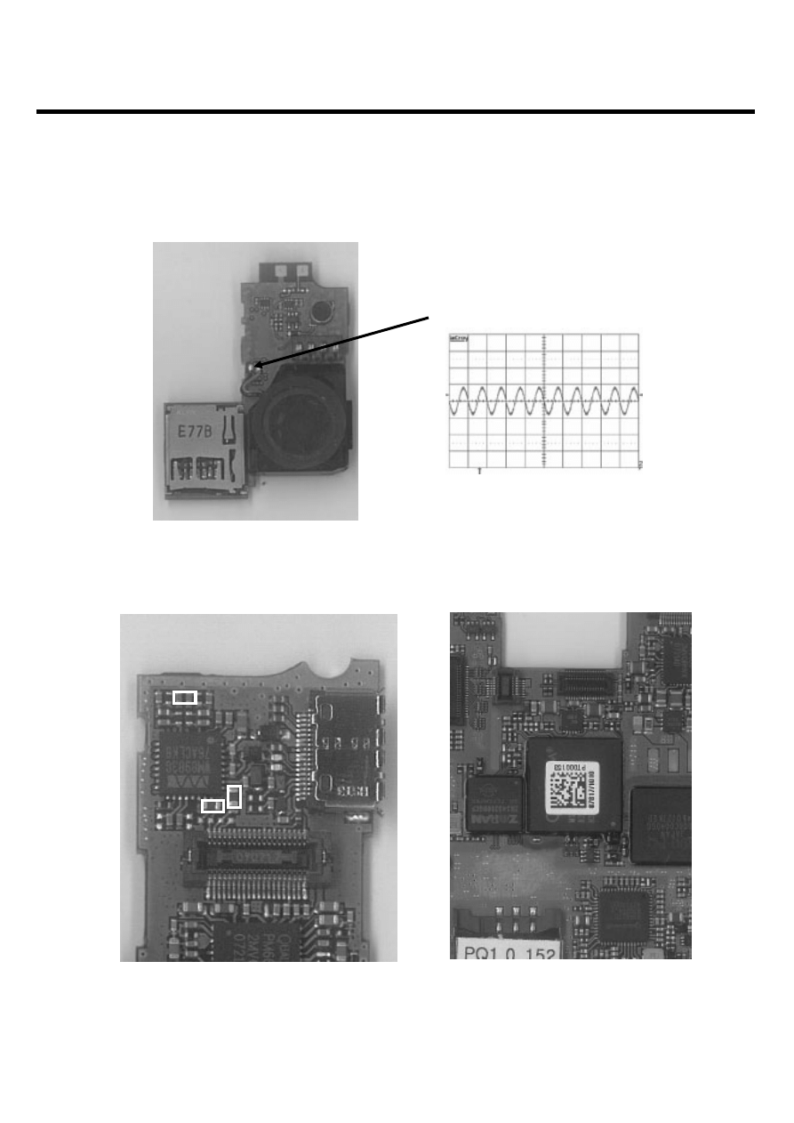
LGE Internal Use Only
Copyright © 2007 LG Electronics. Inc. All right reserved.
Only for training and service purposes
4. TROUBLE SHOOTING
- 131 -
MSM
Pads of Speaker
C722
CN603
U502 (audio codec)
C532,C541
FB500, FB501
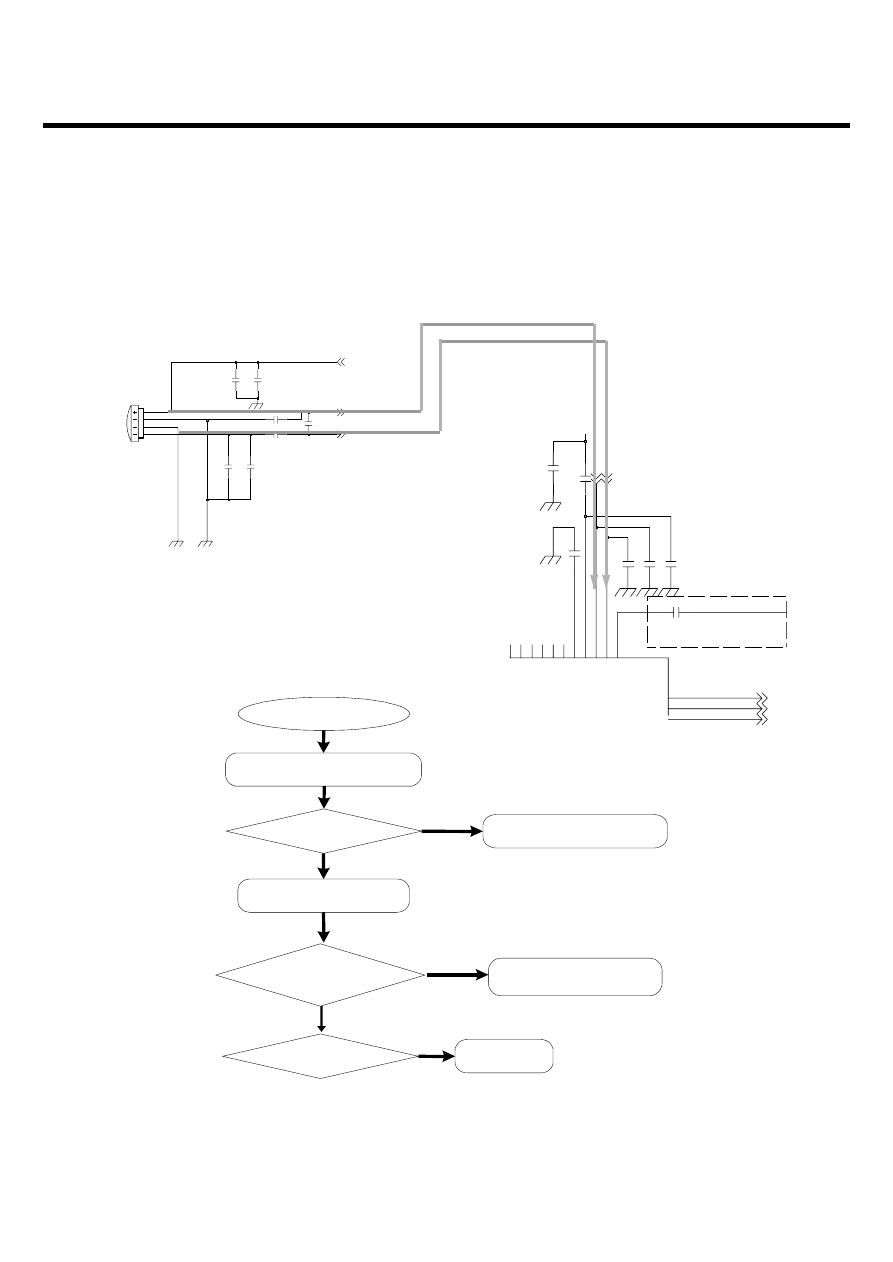
LGE Internal Use Only
Copyright © 2007 LG Electronics. Inc. All right reserved.
Only for training and service purposes
4. TROUBLE SHOOTING
- 132 -
4.12.4 Microphone for main MIC
Main Microphone path as below:
MIC
→ C567,C568 → MSM internal CODEC
MIC
10u
C563
C568
22n
C569
NA
C564
47p
2
G1
3
G2
1
O
4
P
SPM0204HE5-PB-3
MIC500
33p
C575
10p
C576
C567
22n
MICBIAS
MIC1P
MIC1N
10%
Place near
MSM pin W18
(CODEC VSS)
C204
NA
C238
0.1u
0.1u
C235
C236
0.1u
NA
C237
NA
C203
C200
10p
SDCC_DAT1_GPIO99
F25
M25
SDCC_DAT2_GPIO100
SDCC_DAT3_GPIO101
M26
MIC1N
AF20
MIC1P
AE20
AF21
MIC2N
AF22
MIC2P
LINE_L_IN
AC21
LINE_L_IP
AC20
LINE_R_IN
LINE_R_IP
AC19
CCOMP
AA20
AF19
AUXIN
AE19
AUXIP
MSM
MSM
MSM
MIC1P
MIC1N
Can you scoping some
sound signal at C567,C568?
Change the MIC or
Change the Main B'd
NO
YES
YES
make some sound or
voice to MIC
Work well?
END
YES
Start
MIC_BIAS(R221) is 1.8V?
Change the Main B'd
NO
Make a call
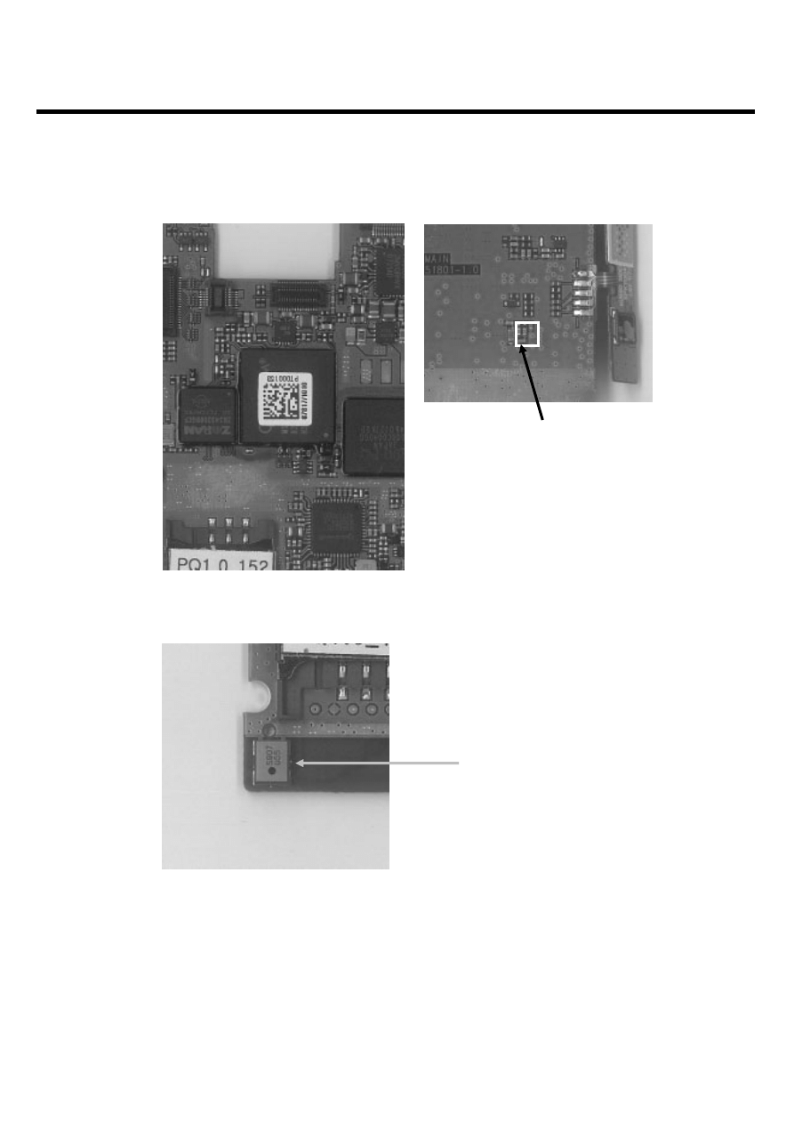
LGE Internal Use Only
Copyright © 2007 LG Electronics. Inc. All right reserved.
Only for training and service purposes
4. TROUBLE SHOOTING
- 133 -
MIC500 (MIC for Handset)
C567, C568
MSM
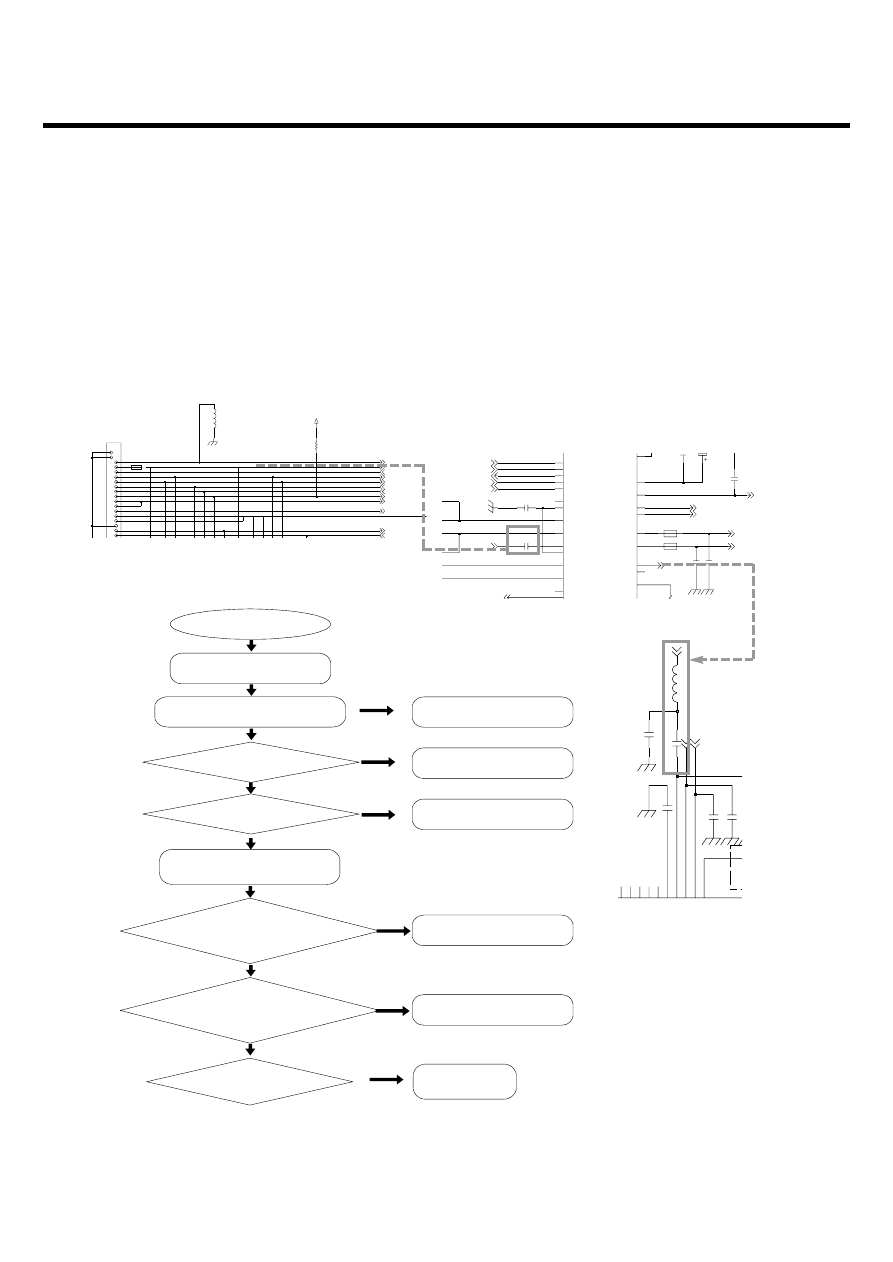
4.12.5 Microphone for headset
MIC for Head_Set path as below:
Insert Headset
→ EAR_SENSE_N(pin8) go 0V → MSM6280 sense Head_Set insertion →
MIC signal
→ U502(audio codec) → MSM6280.
Start
EAR_SENSE_N is 0V?
END
Make a call
Change the Main b'd
Change the Main b'd
MIC_BIAS is 2.7V ?
YES
YES
NO
NO
NO
Try ch ange the head set
Can y ou s coping s ome
sound signal at C539?
Change the MIC
YES
YES
make some sound or
vo ice t o MIC
Work w ell?
END
YES
Can y ou s coping s ome
sound signal at C235,L20 0?
Check t he U502 or
Change the Main Bíd
NO
NO
YES
LGE Internal Use Only
Copyright © 2007 LG Electronics. Inc. All right reserved.
Only for training and service purposes
4. TROUBLE SHOOTING
- 134 -
8
9
12
13
14
15
16
17
19
2
21
3
4
5
6
7
CN500
1
10
11
R528
100K
FB504
VREG_MSMP_2.7V
2.2uH
L504
TV_OUT
EAR_MIC_P
RMT_PWR_ON_N
RMT_INT-USB_D+
RMT_ADC-USB_D-
VBATT
FM_ANT
UART TXD
USB_VBUS
MIDI_EAR_L
MIDI_EAR_R
EAR_SENSE_N
FB501
FB500
R2_GPIO3
6
RIN
5
4
RIP
ROUT1
29
ROUT2
23
16
SCLK
27
VMID
DACDAT
10
L2_GPIO2
3
LIN
2
1
LIP
LOUT1
30
25
LOUT2
7
LRC
11
MCLK
MICBIAS
32
18
MODE
OUT3
22
21
OUT4
ADCDAT
9
24
AGND2
AUXL
19
AUXR
20
8
BCLK
15
CSB_GPIO1
10u
C525
C534
1u
K
9
NA
C531
C539
1u
C524
0.1u
NA
C544
C543
NA
MIC_PWR
MMP_A_MCLK
CODEC I2C SCL
HP_EAR_L
MIC2P
HP_EAR_R
MID_MICP
MMP_A_BCLK
MMP_ADO_DACDAT
MMP_A_LRCLK
MMP_ADI_ADCDAT
SPK_OUT-
SPK_OUT+
C204
NA
C2
0.1u
C235
C236
0.1u
L200
100nH
NA
C203
C200
10p
SDCC_DAT1_GPIO99
SDCC_DAT2_GPIO100
SDCC DAT3 GPIO101
MIC1N
AF20
MIC1P
AE20
AF21
MIC2N
AF22
MIC2P
LINE_L_IN
AC21
AC20
LINE_R_IN
LINE_R_IP
AC19
CCOMP
AA20
AF19
AUXIN
AE19
AUXIP
MIC1P
MIC1N
MIC2P
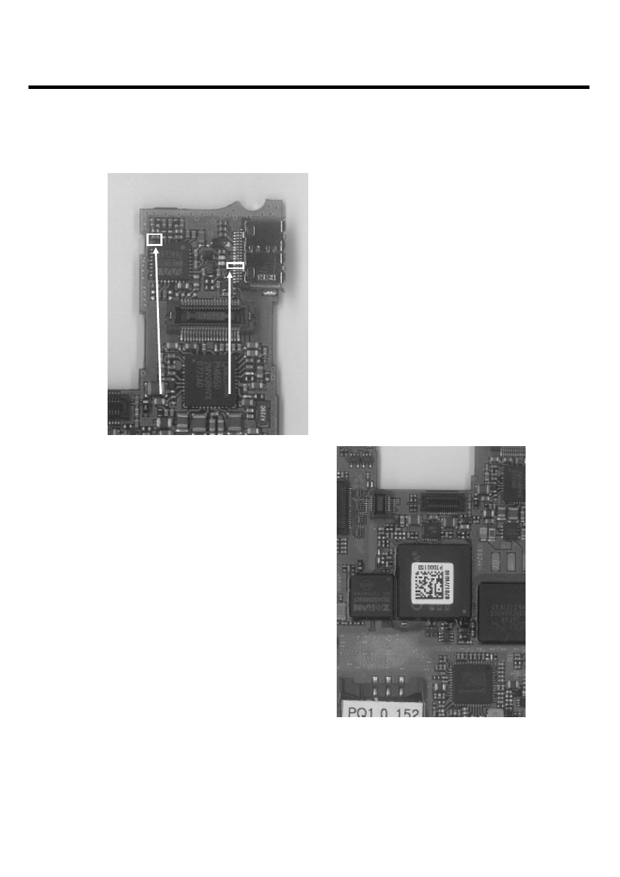
LGE Internal Use Only
Copyright © 2007 LG Electronics. Inc. All right reserved.
Only for training and service purposes
4. TROUBLE SHOOTING
- 135 -
#8 pin of ear connector
to check EAR_SENSE_N
C535
MSM
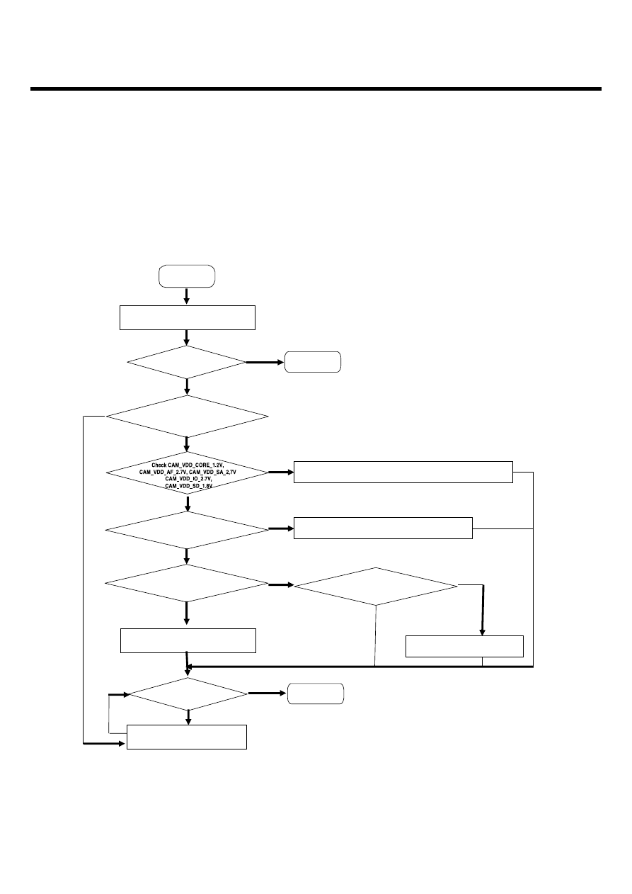
LGE Internal Use Only
Copyright © 2007 LG Electronics. Inc. All right reserved.
Only for training and service purposes
4. TROUBLE SHOOTING
- 136 -
4.13 Camera trouble
Camera control signals are generated by ZORAN (Multimedia Chip)
and directly connected with ZORAN.
KU990 has two cameras. The one is a 5 Mega Camera, the other is VGA camera.
No
Camera is OK?
Check the camera conn. and
reconnect the camera
Change the LDO (U601, U602, U701, U900, U901)
Camera is OK
Check MMP_CAM_PCLK
Change the camera
Yes
NO
NO
Yes
(CN600)
Change the Main board
End
Yes
End
NO
5M START
ZORAN output signal check
(MMP_CAM_RESET_N, MMP_
CAM_PWR_EN))
Yes
NO
Check master clock
5M_CAM_MCLK
(CN600)
Yes
Change the Analog Switch (U604, U607)
NO
Yes
Check the EMI/ESD filter
(FL600, FL601)
Yes
No
Change the Filter
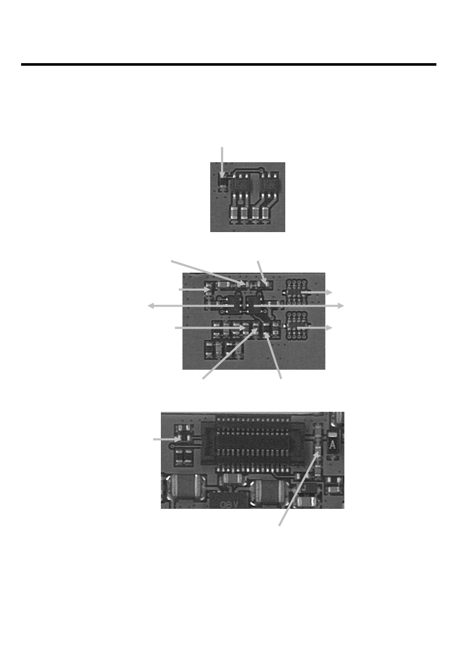
LGE Internal Use Only
Copyright © 2007 LG Electronics. Inc. All right reserved.
Only for training and service purposes
4. TROUBLE SHOOTING
- 137 -
MMP_CAM_RESET_N
MMP_CAM_PWR_EN
CAM_VDD_CORE_1.2V
CAM_VDD_SA_2.7V
CAM_VDD_IO_2.7V
CAM_VDD_SD_1.8V
CAM_VDD_AF_2.7V
FL600
FL601
MMP_CAM_PCLK
5M_CAM_MCLK
U604
U607
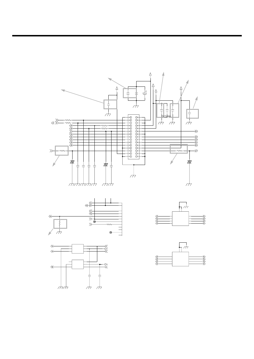
LGE Internal Use Only
Copyright © 2007 LG Electronics. Inc. All right reserved.
Only for training and service purposes
4. TROUBLE SHOOTING
- 138 -
GB042-30S-H10-E3000
1u
CAM_VDD_SA_2.7V
CAM_VDD_IO_2.7V
C608
C605
0.1u
10p
C610
30
17
18
19
20
21
22
23
24
14
15
2
3
4
5
6
7
8
9
16
25
26
27
28
29
CN600
1
10
11
12
13
0.1u
C612
C606
10p
R601 10
R607
33
0.1u
C607
10p
C611
CAM_VDD_AF_2.7V
CAM_VDD_CORE_1.2V
VA601
ICVL0518100Y500FR
VA602
C614
EVLC18S02015
0.1u
C601
0.1u
ICVL0518100Y500FR
VA600
10u
C600
R604
10
CAM_VDD_SD_1.8V
10
R603
10p
C613
C609
0.1u
R608
10
C602
1u
R602 10
STROBE_TRIGGER
MMP_CAM_PCLK
5M_CAM_DATA[0]
5M_CAM_DATA[1]
5M_CAM_DATA[2]
5M_CAM_DATA[3]
5M_CAM_DATA[4]
5M_CAM_DATA[5]
5M_CAM_DATA[6]
5M_CAM_DATA[7]
MMP_CAM_RESET_N
MMP_CAM_INT
MMP_CAM_HSYNC
MMP_CAM_VSYNC
MMP_I2C_SDA
MMP_I2C_SCL
5M_CAM_MCLK
5
G1
10
G2
1
INOUT_A1
INOUT_A2
2
3
INOUT_A3
INOUT_A4
4
9
INOUT_B1
8
INOUT_B2
INOUT_B3
7
6
INOUT_B4
ICVE10184E070R100FR
FL600
G1
5
G2
10
INOUT_A1
1
2
INOUT_A2
INOUT_A3
3
INOUT_A4
4
9
INOUT_B1
INOUT_B2
8
7
INOUT_B3
INOUT_B4
6
FL601
ICVE10184E070R100FR
MMP_CAM_DATA[3]
5M_CAM_DATA[0]
5M_CAM_DATA[1]
5M_CAM_DATA[2]
5M_CAM_DATA[3]
MMP_CAM_DATA[4]
MMP_CAM_DATA[5]
MMP_CAM_DATA[6]
MMP_CAM_DATA[7]
5M_CAM_DATA[4]
5M_CAM_DATA[5]
5M_CAM_DATA[6]
5M_CAM_DATA[7]
MMP_CAM_DATA[0]
MMP_CAM_DATA[1]
MMP_CAM_DATA[2]
U604
NC7SB3157L6X
A
4
B0
3
1
B1
2
GND
6
S
5
VCC
0.1u
C622
NC7SB3157L6X
U607
4
A
3
B0
B1
1
GND
2
S
6
VCC
5
0.1u
C621
+VPWR
+VPWR
5M_CAM_MCLK
CAM_MCLK
VGA_CAM_MCLK
MMP_CAM_MCLK
5M_CAM_MCLK
CAM_SELECT_N
R333
NA
SCL
N14
SDA
P14
GPIO0
P2
M3
GPIO1
GPIO2
P7
N1
GPIO3
GPIO4
P1
GPIO5
M5
N6
GPIO6
GPIO7
M6
P5
GPIO8
N5
GPIO9
TP303
TP302
100K
R331
MMP_CAM_INT
MMP_I2C_SDA
MMP_I2C_SCL
MMP_STROBE_CHARGE
MICROSD_DETECT
MMP_CAM_RESET_N
MMP_CAM_PWR_EN
Schematic of 5M camera part
C605 : CAM_VDD_CORE_1.2V
R607 : 5M_CAM_MCLK
R331 : MMP_CAM_PWR_EN
FL600
FL601
U607
U604
R608 : 5M_CAM_PCLK
C601 : CAM_VDD_AF_2.7V
C609 : CAM_VDD_SA_2.7V
C606 : CAM_VDD_IO_2.7V
C607 :
CAM_VDD_SD_1.8V
LGE Internal Use Only
Copyright © 2007 LG Electronics. Inc. All right reserved.
Only for training and service purposes
4. TROUBLE SHOOTING
- 139 -
Check VGA_VDD_2.7,
VGA_VDD_1.8V
Camera is OK?
Check the camera & 30-pin conn.
And reconnect these connectors
(Main & FPCB connector)
Change the LDO (U600)
Camera is OK
Check the VGA_CAM_PCLK
Yes
NO
NO
Yes
(R718)
Change the Main board
End
Yes
End
NO
VGA START
MSM6280 output signal check
(VGA_CAM_RESET_N, V
VGA_CAM_PWDN)
Yes
NO
Check master clock
(VGA_CAM_MCLK : R717)
Yes
Yes
Check the EMI/ESD filter
Change the Filter (FL700, FL701)
NO
NO
Yes
NO
Change the camera
Yes
No
Change the Analog Switch (U604, U607)
NO
Change the slider FPCB
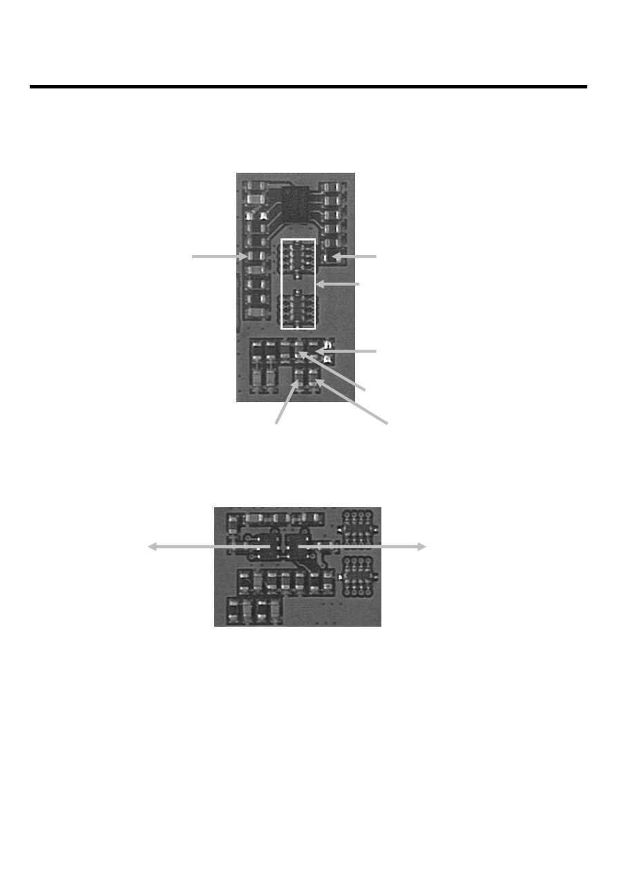
LGE Internal Use Only
Copyright © 2007 LG Electronics. Inc. All right reserved.
Only for training and service purposes
4. TROUBLE SHOOTING
- 140 -
VGA_CAM_PWDN
VGA_CAM_RESET_N
VGA_CAM_PCLK
VGA_CAM_PCLK
FL700, FL701 : EMI FILTER
VGA_VDD_2.7V
U604
U607
VGA_VDD_1.8V
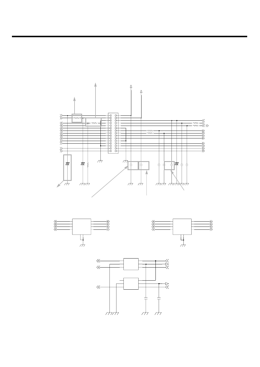
LGE Internal Use Only
Copyright © 2007 LG Electronics. Inc. All right reserved.
Only for training and service purposes
4. TROUBLE SHOOTING
- 141 -
10
R719
VGA_VDD_2.7V
R725
10
10
R724
16
25
26
27
28
29
30
17
18
19
20
21
22
23
24
1
10
11
12
13
14
15
2
3
4
5
6
7
8
9
CN701
C711
0.1u
10p
C713
R718
10
EVLC18S02015
VA715
R729
NA
resistor
10p
C715
10
R717
VA714
ICVL0518100Y500FR
10
R720
C712
10p
EVLC18S02015
VA713
C709
0.1u
VGA_VDD_1.8V
C714
10p
0.1u
C710
VGA_CAM_DATA[2]
VGA_CAM_DATA[3]
VGA_CAM_DATA[4]
VGA_CAM_DATA[7]
I2C_SDA
I2C_SCL
MMP_CAM_VSYNC
MMP_CAM_HSYNC
VGA_CAM_RESET_N
RCV+
RCV-
MOTOR+
MOTOR-
x+
x-
Y+
Y-
VGA_CAM_DATA[6]
VGA_CAM_PWDN
VGA_CAM_DATA[5]
VGA_CAM_MCLK
MMP_CAM_PCLK
VGA_CAM_DATA[0]
VGA_CAM_DATA[1]
6
5
G1
10
G2
INOUT_A1
1
2
INOUT_A2
INOUT_A3
3
4
INOUT_A4
9
INOUT_B1
INOUT_B2
8
7
INOUT_B3
INOUT_B4
ICVE10184E070R100FR
FL701
G1
5
G2
10
INOUT_A1
1
2
INOUT_A2
INOUT_A3
3
4
INOUT_A4
9
INOUT_B1
INOUT_B2
8
7
INOUT_B3
INOUT_B4
6
FL700
ICVE10184E070R100FR
MMP_CAM_DATA[0]
MMP_CAM_DATA[1]
MMP_CAM_DATA[2]
MMP_CAM_DATA[3]
VGA_CAM_DATA[0]
VGA_CAM_DATA[1]
VGA_CAM_DATA[2]
VGA_CAM_DATA[3]
MMP_CAM_DATA[4]
MMP_CAM_DATA[5]
MMP_CAM_DATA[6]
MMP_CAM_DATA[7]
VGA_CAM_DATA[4]
VGA_CAM_DATA[5]
VGA_CAM_DATA[6]
VGA_CAM_DATA[7]
U604
NC7SB3157L6X
A
4
B0
3
1
B1
2
GND
6
S
5
VCC
0.1u
C622
NC7SB3157L6X
U607
4
A
3
B0
B1
1
GND
2
S
6
VCC
5
0.1u
C621
+VPWR
+VPWR
5M_CAM_MCLK
CAM_MCLK
VGA_CAM_MCLK
MMP_CAM_MCLK
5M_CAM_MCLK
CAM_SELECT_N
Schematic of VGA camera part
R717 : VGA_CAM_MCLK
VA713 : VGA_VDD_2.7V
VA713 : VGA_VDD_2.7V
FL700
FL701
U604
U607
VA713 : VGA_CAM_PWDN
C709 : VGA_VDD_1.8V
R718 : VGA_CAM_PCLK
LGE Internal Use Only
Copyright © 2007 LG Electronics. Inc. All right reserved.
Only for training and service purposes
4. TROUBLE SHOOTING
- 142 -
4.14 Main LCD trouble
Main LCD control signals are generated by MSM6280. Those signal’s path are :
MSM6280
→ Z ORAN (Multimedia Chip) -> 40-pin connector(CN300 in Main PCB) -> 40-pin connector
(in LCD Module)
The LCD works
START
Press END key
to turn the power on
Is the circuit powered?
Follow the Power ON
trouble shooting
LCD display OK?
Check LCD_VDD_2.8V, LCD_RESET_N,
LCD_DATA[0~15] in Main BD
No
Yes
Yes
No
Disconnect and reconnect
40-pin B to B connector
Change the Main BD
No
End
Yes
Display OK?
Yes
Change the LCD module
No
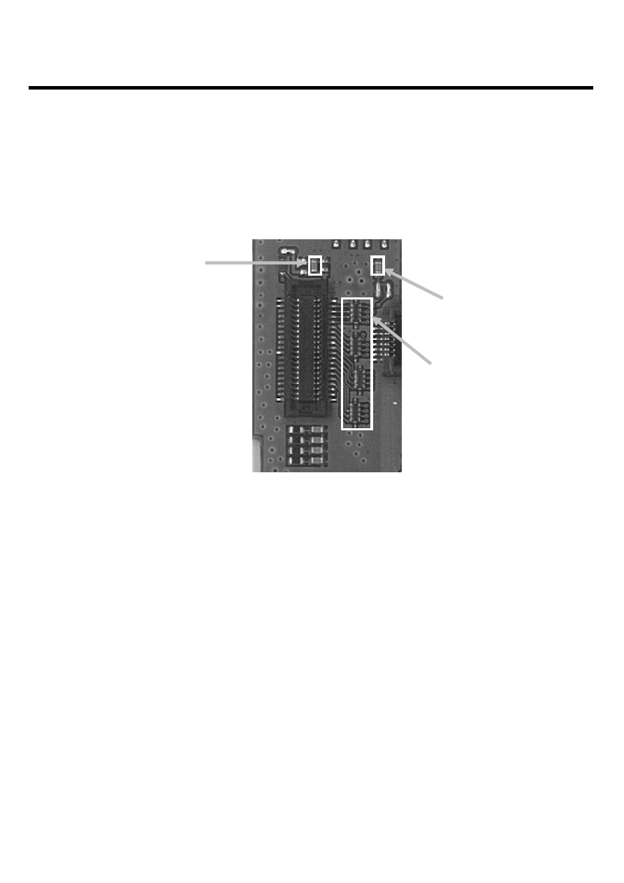
LGE Internal Use Only
Copyright © 2007 LG Electronics. Inc. All right reserved.
Only for training and service purposes
4. TROUBLE SHOOTING
- 143 -
Main BD
SUB BD
LCD_NRESET
LCD_VDD_2.8V
LCD_DATA[0~15]
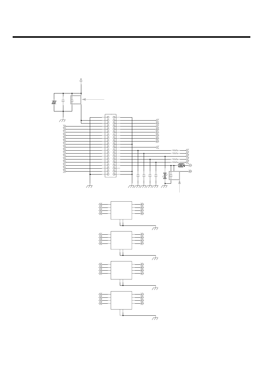
- 144 -
4. TROUBLE SHOOTING
LGE Internal Use Only
Copyright © 2007 LG Electronics. Inc. All right reserved.
Only for training and service purposes
OTP Program Pin
ENBY0036001
1.0T, Socket
GB042-40S-H10-E3000
7
INOUT_B3
INOUT_B4
6
FL301 ICVE10184E150R500FR
G1
5
G2
10
INOUT_A1
1
2
INOUT_A2
INOUT_A3
3
4
INOUT_A4
9
INOUT_B1
INOUT_B2
8
C322
22p
C323
22p
R315
51
22p
C325
VA300
ICVN0505X150FR
25
26
27
28
29
9
21
30
31
32
33
34
35
36
37
38
39
22
40
23
24
12
13
14
15
16
17
18
19
2
20
3
4
5
6
7
8
CN300
1
10
11
VA301
51
R314
NA
C320
C326
22p
G2
1
INOUT_A1
INOUT_A2
2
3
INOUT_A3
INOUT_A4
4
INOUT_B1
9
8
INOUT_B2
INOUT_B3
7
6
INOUT_B4
ICVE10184E150R500FR
FL303
5
G1
10
51
R316
R318
0
5
G1
10
G2
1
INOUT_A1
INOUT_A2
2
3
INOUT_A3
INOUT_A4
4
INOUT_B1
9
8
INOUT_B2
INOUT_B3
7
6
INOUT_B4
ICVE10184E150R500FR
FL300
51
R317
22p
C324
0.1u
C321
6
FL302 ICVE10184E150R500FR
G1
5
G2
10
INOUT_A1
1
2
INOUT_A2
INOUT_A3
3
4
INOUT_A4
9
INOUT_B1
INOUT_B2
8
7
INOUT_B3
INOUT_B4
LCD_VDD_2.8V
LCD_VSYNC_OUT
LCD_MAKER_ID
MMP_LCD_WE_N
MMP_LCD_VSYNC_OUT
WLED_PWR
WLED_2
WLED_4
WLED_5
MMP_LCD_VSYNC_IN
LCD_IF_MODE
LCD_DATA[0]
LCD_DATA[1]
LCD_DATA[2]
LCD_DATA[3]
LCD_DATA[4]
LCD_DATA[5]
LCD_DATA[6]
LCD_DATA[7]
LCD_DATA[14]
LCD_DATA[15]
LCD_DATA[8]
LCD_DATA[9]
LCD_DATA[10]
LCD_DATA[11]
LCD_DATA[12]
LCD_DATA[13]
WLED_1
WLED_3
MMP_LCD_ADS
MMP_LCD_CS_N
LCD_RESET_N
MMP_LCD_RD_N
MMP_LCD_DATA[9]
MMP_LCD_DATA[10]
MMP_LCD_DATA[11]
MMP_LCD_DATA[12]
MMP_LCD_DATA[13]
MMP_LCD_DATA[14]
MMP_LCD_DATA[15]
LCD_DATA[12]
LCD_DATA[13]
LCD_DATA[14]
LCD_DATA[15]
MMP_LCD_DATA[0]
MMP_LCD_DATA[1]
MMP_LCD_DATA[2]
MMP_LCD_DATA[3]
MMP_LCD_DATA[4]
MMP_LCD_DATA[5]
MMP_LCD_DATA[6]
MMP_LCD_DATA[7]
MMP_LCD_DATA[8]
LCD_DATA[0]
LCD_DATA[1]
LCD_DATA[2]
LCD_DATA[3]
LCD_DATA[4]
LCD_DATA[5]
LCD_DATA[6]
LCD_DATA[7]
LCD_DATA[8]
LCD_DATA[9]
LCD_DATA[10]
LCD_DATA[11]
Schematic of LCD part
C321 : LCD_VDD_2.8V
C326 : LCD_VDD_2.8V
FL300
FL301
FL302
FL303
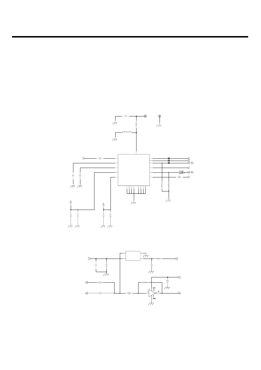
- 145 -
4. TROUBLE SHOOTING
LGE Internal Use Only
Copyright © 2007 LG Electronics. Inc. All right reserved.
Only for training and service purposes
4.15 Bluetooth trouble
Bluetooth supplied voltages are generated by the PM6650.
Those signal’s path are : PM6650
→ VREG_MSMP_2.7V and VREG_BT_2.85V is asserted →
TCXO_BT 19.2MHz is asserted
→ Bluetooth ON → BT_TX_RX_N is High → BT serial interface
control is operated (SBST / SBCK / SBDT)
BLUETOOTH
LG INNOTEK
TP802
TP801
10K
R809
C804
1u
C802
1000p
0
R807
C803
1u
C800
NA
0
R800
BT_ANT
C814
2.2u
C811
100p
C812
0.1u
GND3
GND4
15
17
PGND1
PGND2
18
19
PGND3
PGND4
20
RX_BB_TX_BB
13
SBCK
11
12
SBDT
SBST
4
5
SYNC_DET_TX_EN
3
VCC_OUT
14
VDD_BAT
VDD_INT
2
VDD_MSM
10
7
XTAL_IN
M800
LBRQ-2B43A
ANT
16
9
CLK_REF
1
GND1
GND2
6
8
BT_GND
100p
C813
C801
NA
L800
1000p
VREG_BT_2.85V
VREG_MSMP_2.7V
TP800
10K
R808
BT_DATA
BT_CLK
BT_SBCK
BT_SBDT
BT_SBST
BT_TX_RX_N
TCXO_BT
TCXO
0.1u
C139
C147
1000p
100ohm
R115
1000p
C145
0.01u
C141
8200p
C148
1000p
C140
X100
2
GND
OUT
3
VCC
4
VCONT
1
19.2MHz
R120 100K
TC7SH04FS
U102
C144
1000p
TRK_LO_ADJ
VREG_TCXO_2.85V
TCXO_BT
VREG_BT_2.85V
TCXO_PM
RTR6275_TCXO
Figure. Schematic of Bluetooth Interface
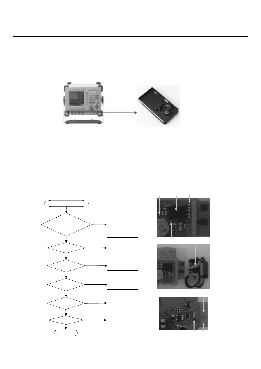
4.16 Bluetooth RF Test
TC-3000A (Bluetooth Tester)
1. Set phone to bluetooth test-mode.
- Enter Test Mode(3845#*990#)
→ Module Test Set → BT DUT → BT DUT ON
2. Insert a phone in a TEMSELL (in case of radiation test)
3. Set ‘discover’ after push menu button of the tester and select the link analyzer .
4. After ‘set test mode’, confirm the connection state.
5. Measure the power of full channel after hopping mode is selected to ‘ON’
6. You can select wanted test cases after getting an optimized power
- 146 -
4. TROUBLE SHOOTING
LGE Internal Use Only
Copyright © 2007 LG Electronics. Inc. All right reserved.
Only for training and service purposes
M800
BT_ANT
BT Antenna
TP800
TP801
TP802
BT_GND
R800
Set the bluet oot h ON
VREG_BT_2.85V
and
VREG_MSMP_2.7V
is ass erted?
Check P MIC
(U501) Pin#64
XTAL_IN
is ass erted?
Check Os ci llator
(X100)
An d
Check Buffer
(U102)
CLK_REF
is ass erted?
Check sol deri ng
of BT( M800)
No
No
No
Yes
Yes
Yes
SYNC_DET_TX_EN
is ass erted?
Check sol deri ng
of BT( M800)
No
Yes
SBST/SBCK/SBDT
is ass erted?
Check
TP800/TP801/ P802
No
Yes
Bluetoot h is work well?
Change
the main board
END
No
Yes
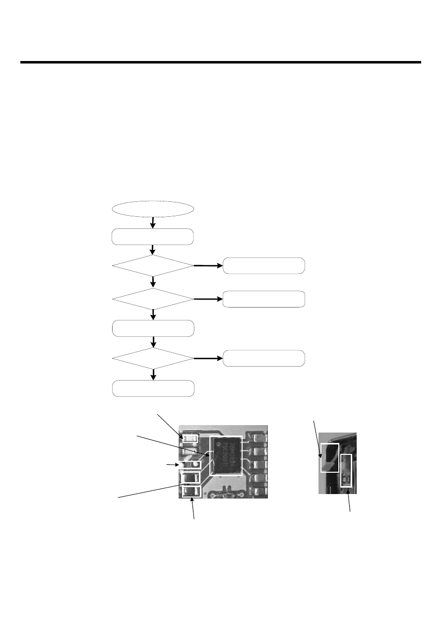
- 147 -
4. TROUBLE SHOOTING
LGE Internal Use Only
Copyright © 2007 LG Electronics. Inc. All right reserved.
Only for training and service purposes
4.17 Touch Screen trouble
Touch Initial sequence of KU990 is:
LCD_VDD_2.8V(C701) goes to 2.8V
→ TOUCH_PENIRQ_N(R702),TOUCH_I2C_SCL(R703) &
TOUCH_I2C_SDA(R704) go to high Touch operation of KU990 is :
A finger is touching on the screen -> TOUCH_PENIRQ_N is low -> I2C is connected -> A finger is
took off from the Screen -> TOUCH_PENIRQ_N is high -> I2C is not connected.
Start
Work well?
Connector Is insert?
Replace the Main board
End
Insert Connector, again
Yes
No
YES
NO
Touchpad Calibration
Replace the Folder
Work well?
End
Yes
No
R702 (TOUCH_PENIRQ_N)
R704(TOUCH_I2C_SDA)
U700
R703 (TOUCH_I2C_SCL)
C701 (LCD_VDD_2.8V)
Touch Window Connector
VGA FPCB Connector
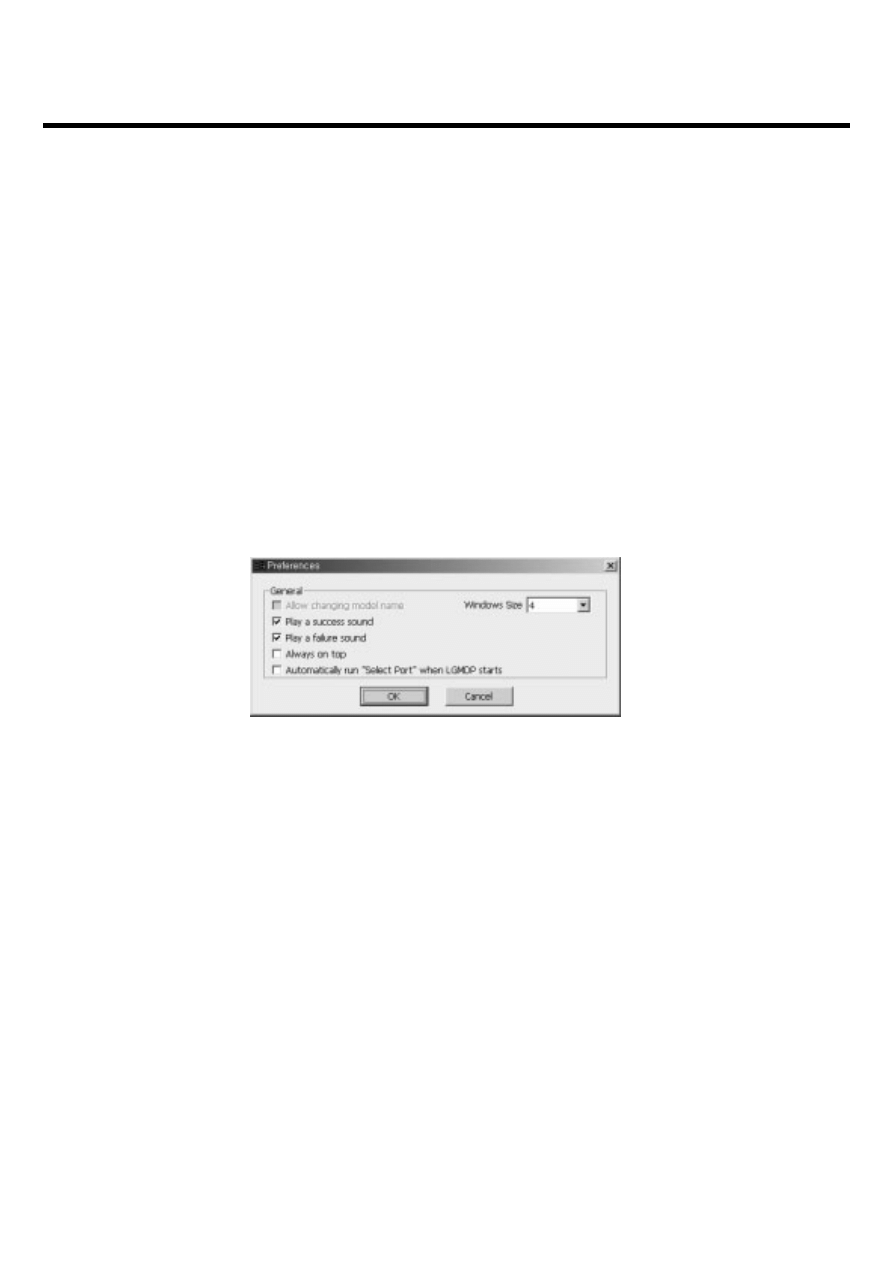
- 148 -
5. DOWNLOAD
5.1 Introduction
LGMDP is a LGE application that allow users to download images from PC to handset. LGMDP is a
download tool with capabilities to upload image files to the handset. LGMDP is designed to be simple
to use and easy enough for the beginner to upload executable images to the handset. LGMDP
supports Windows 2000/XP where the LG (Ver 4.6 or later) USB modem driver is installed.
Additionally, LGMDP allows multi downloading up to 9 handsets at the same time.
5.2 Downloading Procedure
• Connect the phone to your desktop PC using the USB cable and run the LGMDP application. Before
getting started, set up LGMDP preferences from the Preferences of the file menu the way you want.
Click on the File menu and select Preferences.
➢ Play a success sound
It will be played a .wav file when the download has been completed. To enable this simply check the
box.
➢ Always on Top
Check if LGMDP always appears at the top of the window so that user can monitor it all the time.
➢ Automatically run Select Port When LGMDP starts
When LGMDP starts, it will automatically select Select Port button to download new image file.
5. DOWNLOAD
LGE Internal Use Only
Copyright © 2007 LG Electronics. Inc. All right reserved.
Only for training and service purposes
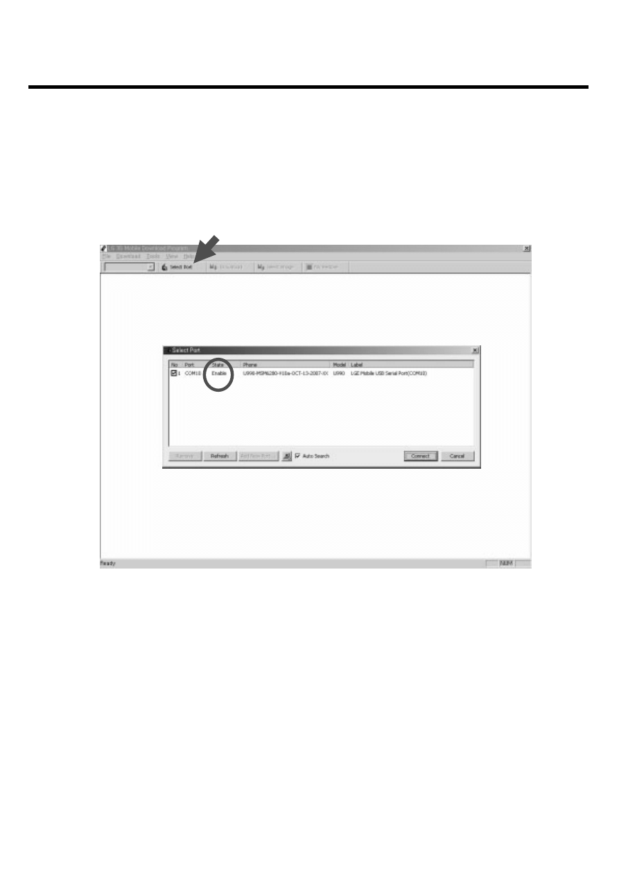
- 149 -
5. DOWNLOAD
LGE Internal Use Only
Copyright © 2007 LG Electronics. Inc. All right reserved.
Only for training and service purposes
5.2.1 Connecting to PC
• Click on the Select Port and then Select Port window will be pop up. Check if state shows Enable for
the port to be connected for downloading images. Then click on the Connect button.
(The port number(COM7) shall be different from that of the port number in the snapshot.)
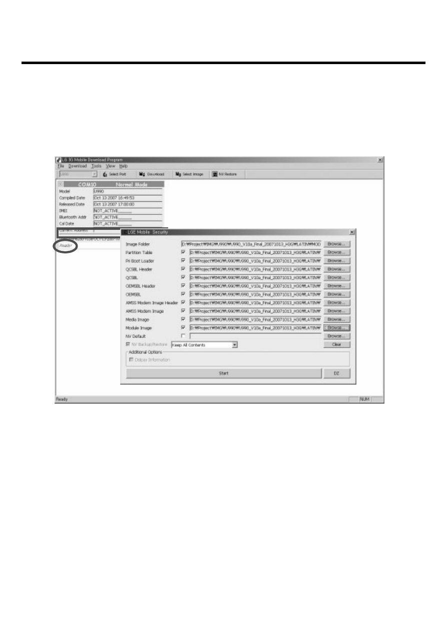
• The status Ready is displayed when the application is ready for downloading. While the images are
transmitted from PC to the handset, a progressive bar
(Red box) indicating the degree of transmission of data is displayed.
- 150 -
5. DOWNLOAD
LGE Internal Use Only
Copyright © 2007 LG Electronics. Inc. All right reserved.
Only for training and service purposes
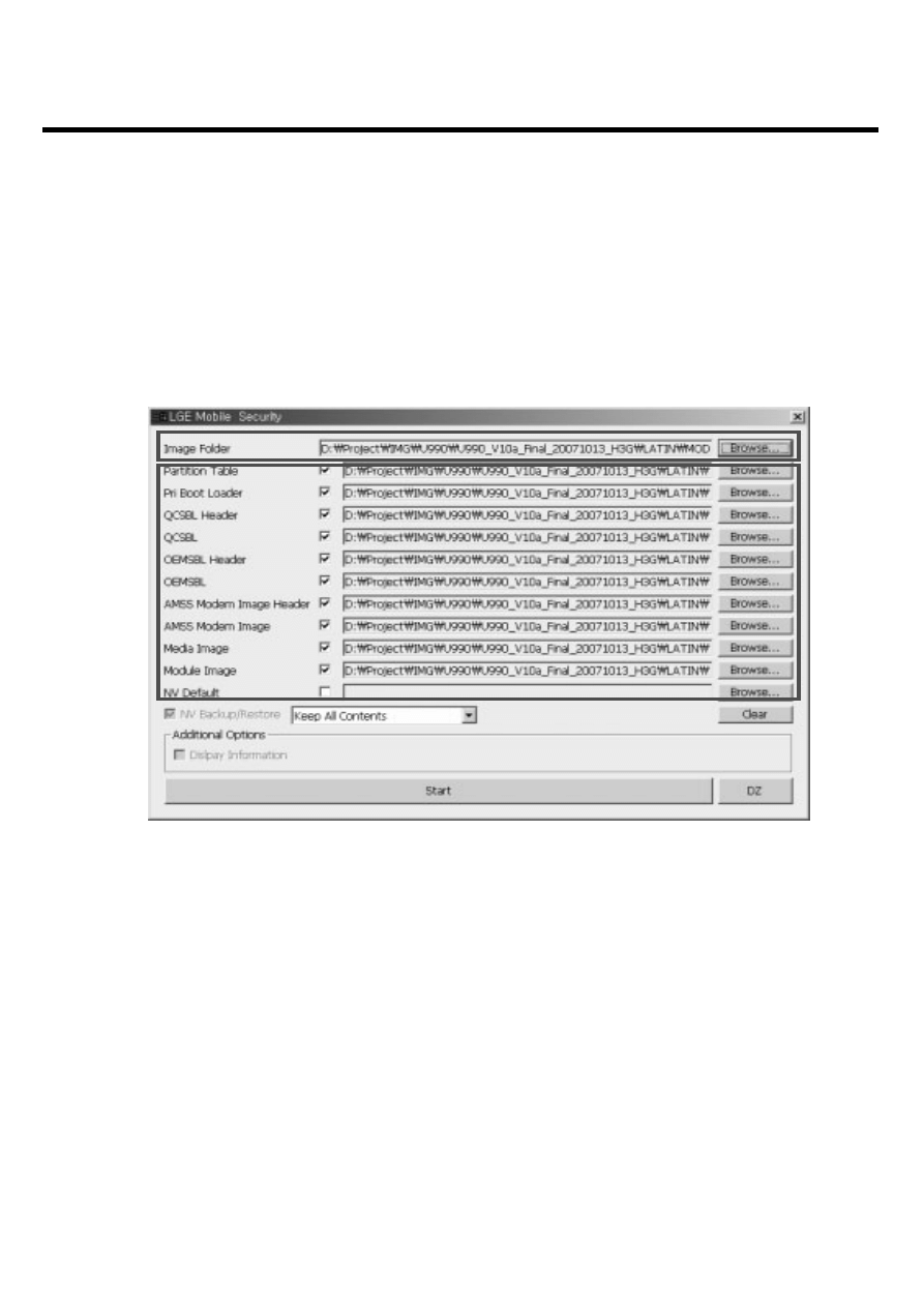
- 151 -
5. DOWNLOAD
LGE Internal Use Only
Copyright © 2007 LG Electronics. Inc. All right reserved.
Only for training and service purposes
1) Image Folder indicates loot path where all image files are placed. To change location of the default
image path, select Browse... button. The edit box shows the file path where images are located.
Please note that all images should be located in a selected folder.
2) Click on the Browse... button to select image files to be downloaded on the handset.
3) NV Backup/Restore: NV Backup/Restore always have to be done, and it is default selected option.
Backup the NV data and restore the backed up NV data automatically.
1)
2)
3)
6)
4)
5)
7)

LGE Internal Use Only
Copyright © 2007 LG Electronics. Inc. All right reserved.
Only for training and service purposes
5. DOWNLOAD
- 152 -
4) Reset database & Contents:
User related data including the setting data on the EFS is reset in the handset. The user contents in
the handset will be erased. If you want to reset all the user data back to the way they were before
you started downloading new images, check the option.
Erase_EFS:
The calibration data, user contents, media, and module are erased. Only calibration data is kept when
NV backup/restore is checked. The user contents and file system physically are wiped out.
Keep All Contents
Maintain user data including WAP, AD, DRM, E-mail, Play lists, and images when downloading a new
S/W images. User data stated above are maintained if this option is selected.
5) Additional Options:
Display Information is defaultly not selected and user cannot choose.
Override partition table is also also defaultly not selected and user cannot choose.
6) Clear: Clearing all directory paths of images in the dialog.
7) Start: Starting downloading the selected individual image.
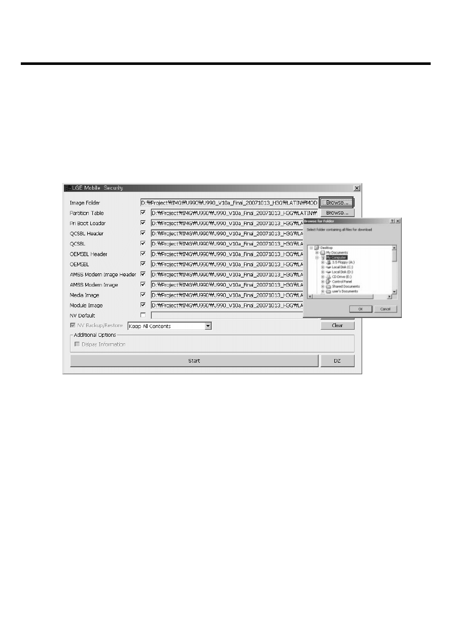
LGE Internal Use Only
Copyright © 2007 LG Electronics. Inc. All right reserved.
Only for training and service purposes
5. DOWNLOAD
- 153 -
5.2.2 Choosing image files
• Select the image folder, where all the image files are located, by clicking on the Browse....
(The folder name shall be different from that of the folder name in the snapshot. The folder name
indicates the path where the image files are located.)
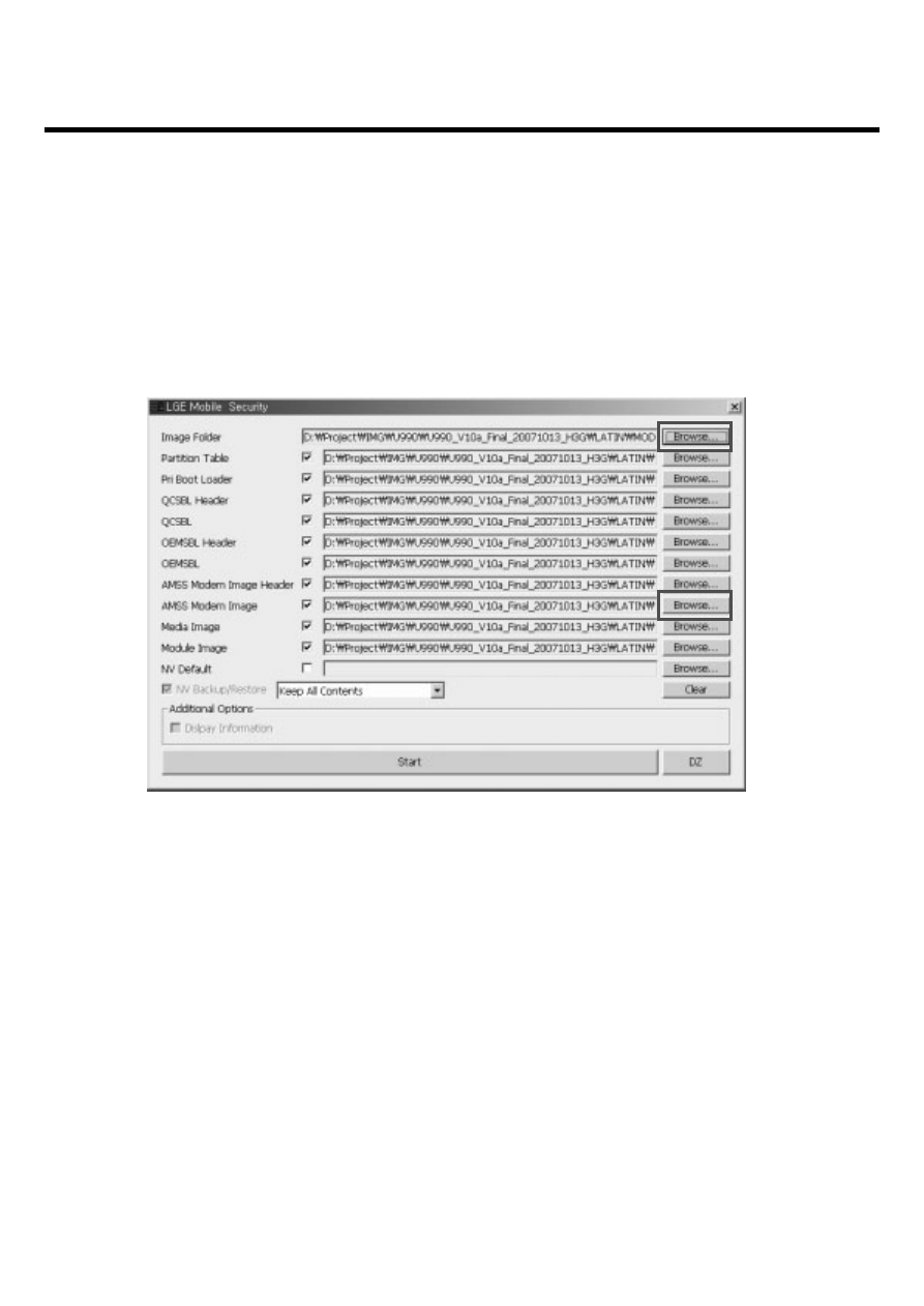
LGE Internal Use Only
Copyright © 2007 LG Electronics. Inc. All right reserved.
Only for training and service purposes
5. DOWNLOAD
- 154 -
Select the path on the Image Folder by clicking on the Browse..., then the LGMDP will automatically
load images accordingly. Also you can select images by manually. For instance, select the path of
AMSS Modem Image file by clicking on the Browse... button. The selected AMSS image will be
downloaded to the handset from the path directory in the PC. Make sure that you have chosen
correct file. In case of wrong AMSS Modem file is selected, the phone may not work.
(The file name shall be different from that of the file name in the snapshot.)
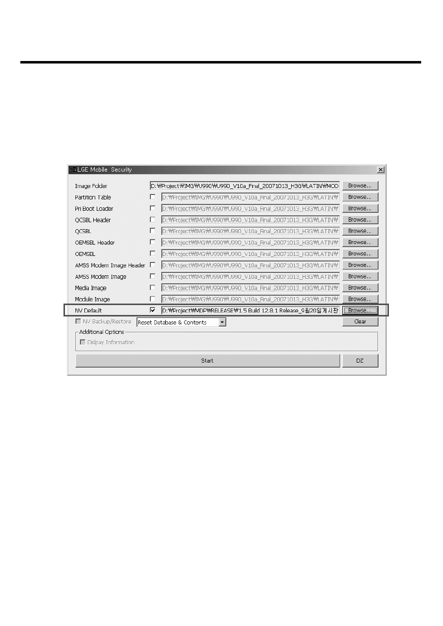
LGE Internal Use Only
Copyright © 2007 LG Electronics. Inc. All right reserved.
Only for training and service purposes
5. DOWNLOAD
- 155 -
• If NV restore is failed, then the NV Data(*.nv2) is erased permanently. In this case, choose the
desired NV file to be downloaded on the handset. To enable this simply check the box or select the
NV file from the LGMDP installation directory by clicking on the Browse... button.
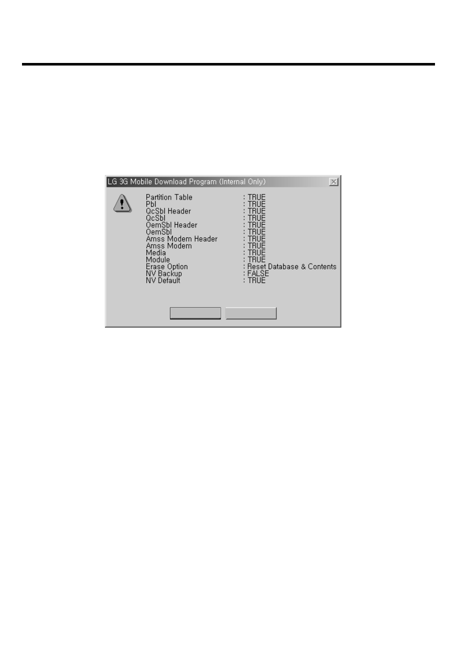
LGE Internal Use Only
Copyright © 2007 LG Electronics. Inc. All right reserved.
Only for training and service purposes
5. DOWNLOAD
- 156 -
Click on the START button to start downloading. A summary of the selected images and option
information window will be displayed. Click on the No button if this is not the setting you are
downloading for. Otherwise click on the Yes button to continue downloading selected image file with
options.
No
Yes
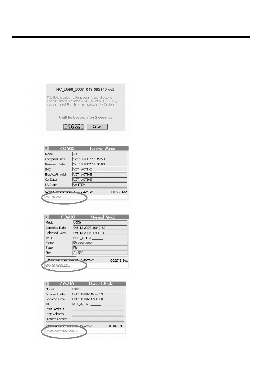
LGE Internal Use Only
Copyright © 2007 LG Electronics. Inc. All right reserved.
Only for training and service purposes
5. DOWNLOAD
- 157 -
• This message box informs that a new file for
NV backup will be created in the displayed
file name in the LGMDP installation
directory.
• Backing up NV data and backed up NV data
will be stored in the LGMDP installation
directory.
• Erasing the existing directories and files
before the Module image is downloaded.
• Downloading the AMSS modem image
5.2.3 Downloading
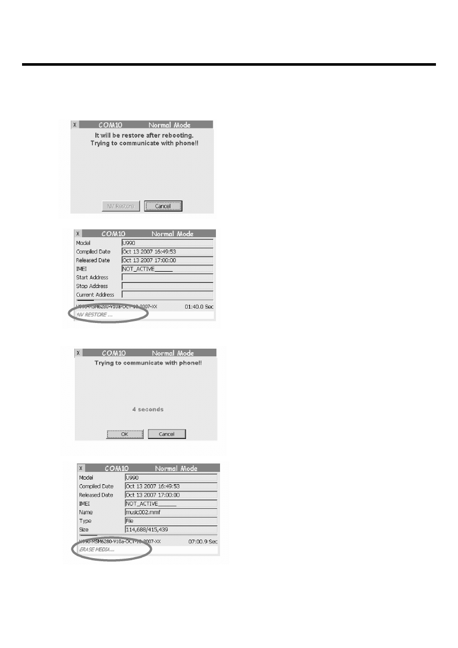
LGE Internal Use Only
Copyright © 2007 LG Electronics. Inc. All right reserved.
Only for training and service purposes
5. DOWNLOAD
- 158 -
• Rebooting the handset and re-establishing
the connection
• Restoring NV data which backed up in the
Backing up process. User can also restore
NV data using NV Default image selection.
• Rebooting the handset and re-establishing
the connection
• Erasing the existing directories and files
before downloading the selected Media
image
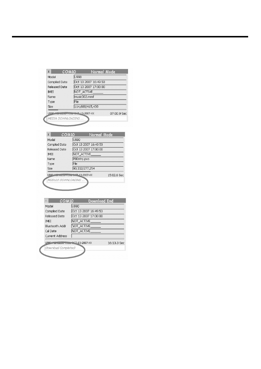
- 159 -
5. DOWNLOAD
LGE Internal Use Only
Copyright © 2007 LG Electronics. Inc. All right reserved.
Only for training and service purposes
• Downloading Media image in progress
• Downloading Module image in progress
• Downloading process has completed
successfully
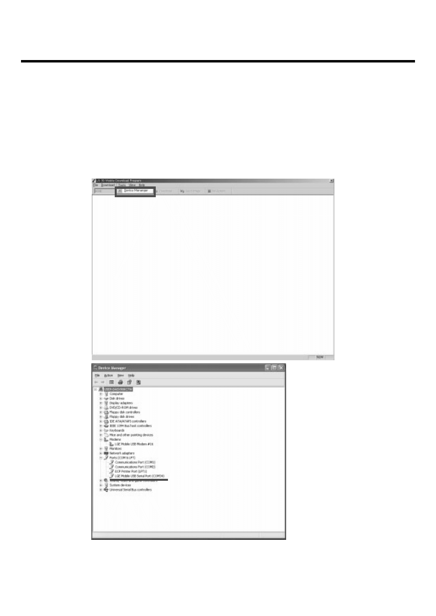
5.2.4 Tools
• Device Manager allows to monitor current hardware that is installed on your PC. Device Manager is
designed to monitor USB connectivity and check where the COM has been installed . Select Device
Manager from the Tools of the file menu.
- 160 -
5. DOWNLOAD
LGE Internal Use Only
Copyright © 2007 LG Electronics. Inc. All right reserved.
Only for training and service purposes
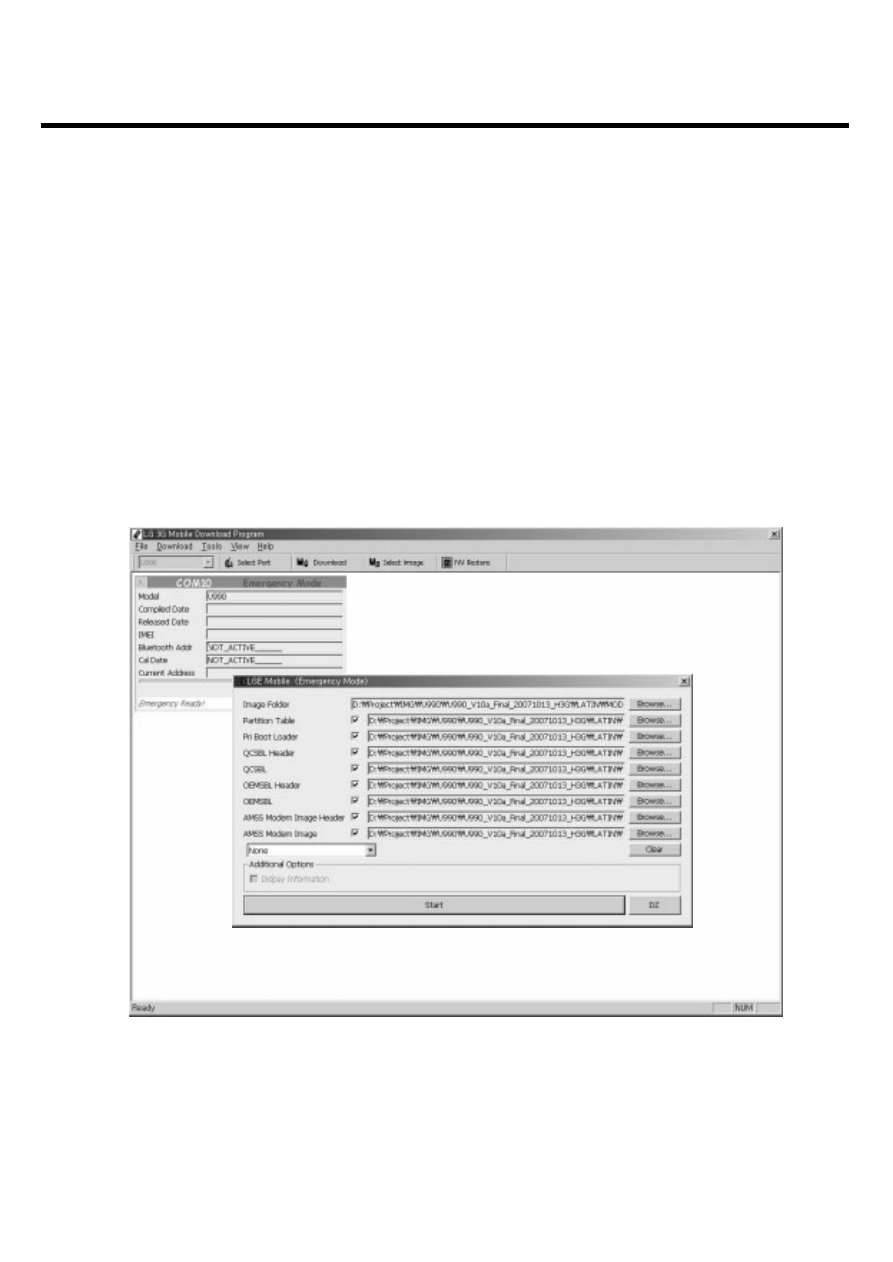
- 161 -
5. DOWNLOAD
LGE Internal Use Only
Copyright © 2007 LG Electronics. Inc. All right reserved.
Only for training and service purposes
5.3 Troubleshooting Download Errors
5.3.1 When the phone does not work
• Reboot the phone in the emergency mode (Simultaneously press 2, 5, and PWR red keys) and
then try to download all the images up to AMSS. In the emergency mode, you can not download
media or module image.
The phone supports a special mode called emergency mode. In this mode, minimum units for
downloading is running so that users can download the images again in case of emergency
situation. (AMSS modem, Media, and Module images can not be running in this mode.)
• The below dialog shows parameters of Select Port when phone is booted in Emergency mode.
Click on the Connect button to continue.
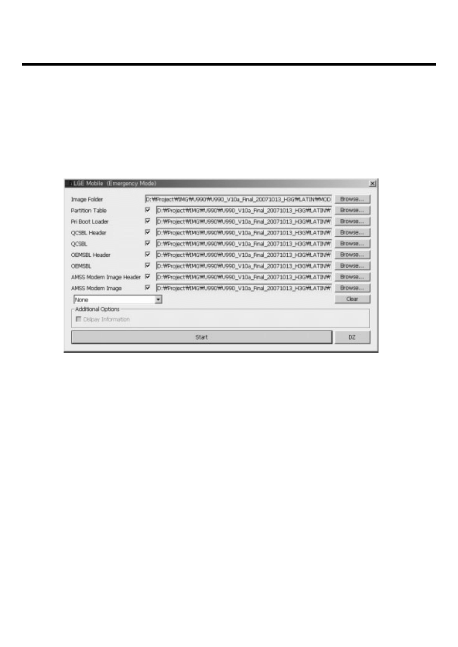
• Choose Image file after clicking on the Browse... button. Make sure that you have chosen the right
image file. After choosing valid images, then click on the Start button to start downloading selected
images. The selected image will be downloaded to the handset from the path directory in the PC.
After downloading images successfully, it will boot to normal mode.
- 162 -
5. DOWNLOAD
LGE Internal Use Only
Copyright © 2007 LG Electronics. Inc. All right reserved.
Only for training and service purposes
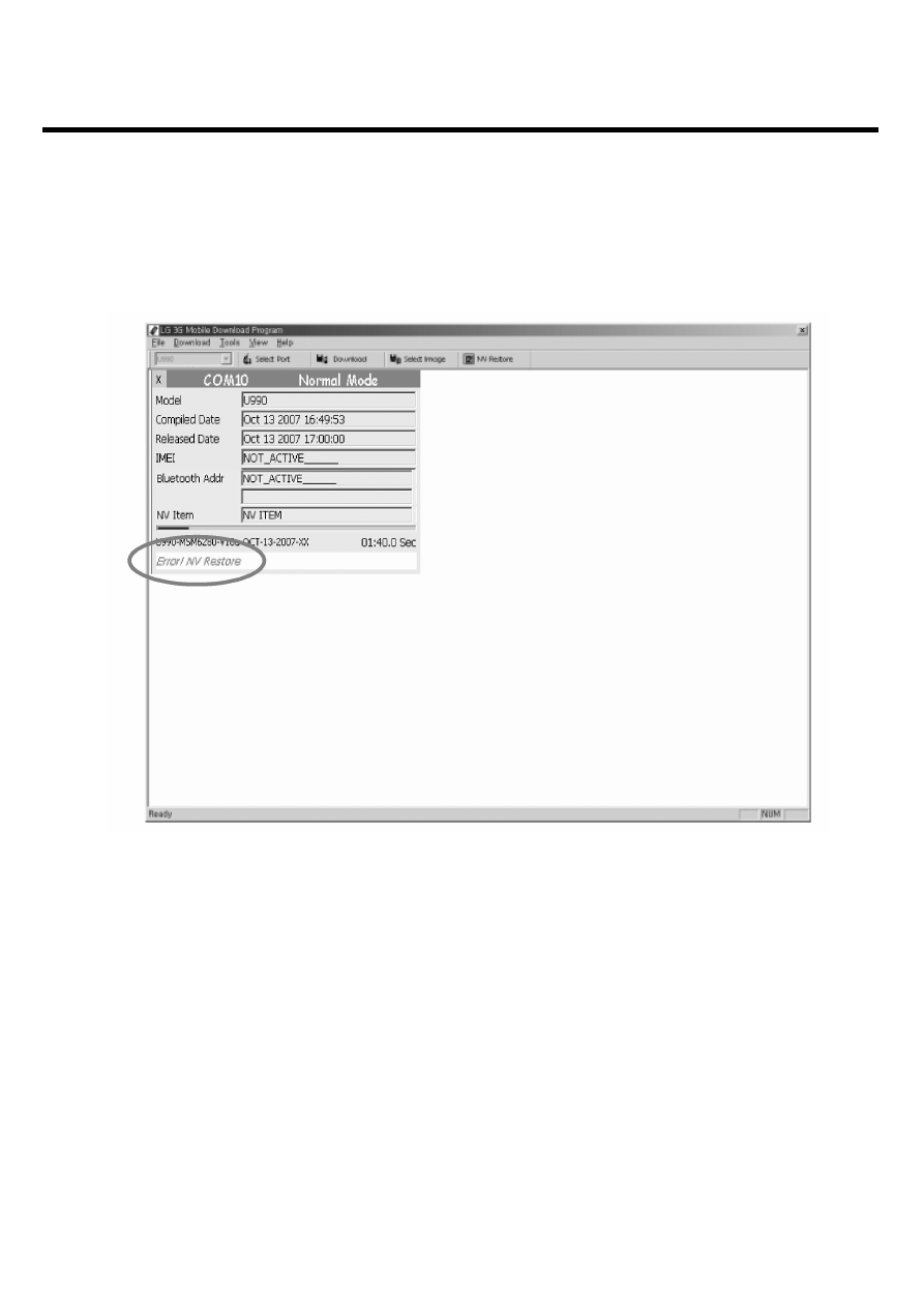
- 163 -
5. DOWNLOAD
LGE Internal Use Only
Copyright © 2007 LG Electronics. Inc. All right reserved.
Only for training and service purposes
5.3.2 NV Restore Error
• Snapshot showing the NV Restore error. Next slide shows the remedial procedure to adopt.
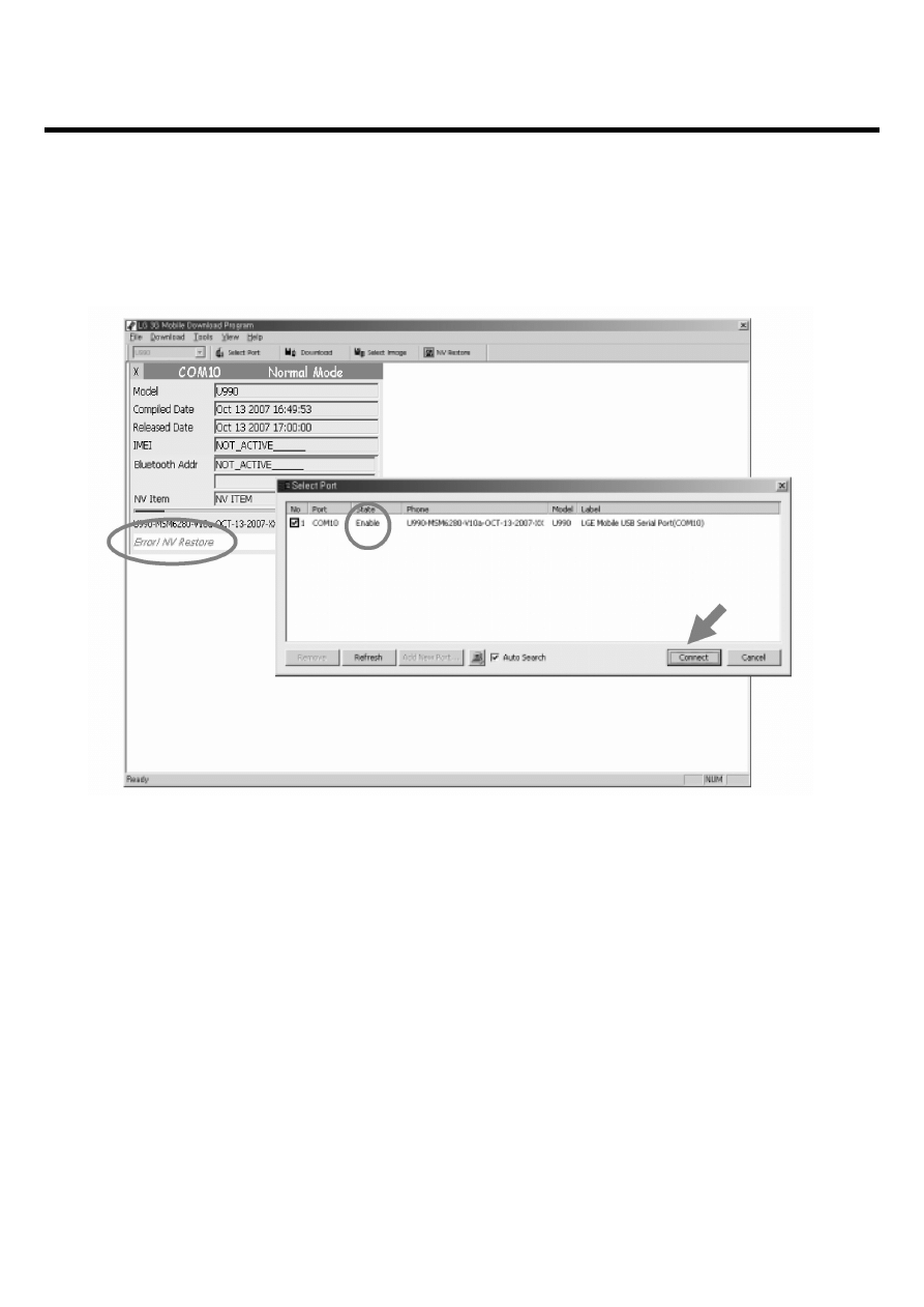
• Connect the handset and Press the Connect button in the Select Port window.
(Enable state in the window indicates that the Phone has been detected and is ready to download.)
- 164 -
5. DOWNLOAD
LGE Internal Use Only
Copyright © 2007 LG Electronics. Inc. All right reserved.
Only for training and service purposes

- 165 -
5. DOWNLOAD
LGE Internal Use Only
Copyright © 2007 LG Electronics. Inc. All right reserved.
Only for training and service purposes
• Click on Browse... . Select the LGMDP installation directory and a list of NV Backup files(*.nv2) will
be shown. These nv files were saved every time NV Backup option was selected, and the name of
the nv file is determined based on the time when NV Backup was done. Choose the desired NV file
to be downloaded on the handset, and click on Start.
5.4 Caution
1) Multi-downloading using the USB hub is not recommendable.
2) If you see the message ‘cal mode’ after ‘completing download’, you must do NV restore and image
(media and module) download.
3) The NV data saved at LGMDP folder as following format.
4) Recommended that the Module and Media Image have to be downloaded at the same time.
5) Erase EFS option will erase everything (media, module, nv items, and user data) in the EFS area.
- 166 -
5. DOWNLOAD
LGE Internal Use Only
Copyright © 2007 LG Electronics. Inc. All right reserved.
Only for training and service purposes
D:\LGMDP\004400-01-429926\_COM14_
LGMDP folder name
IMEI number
Port number
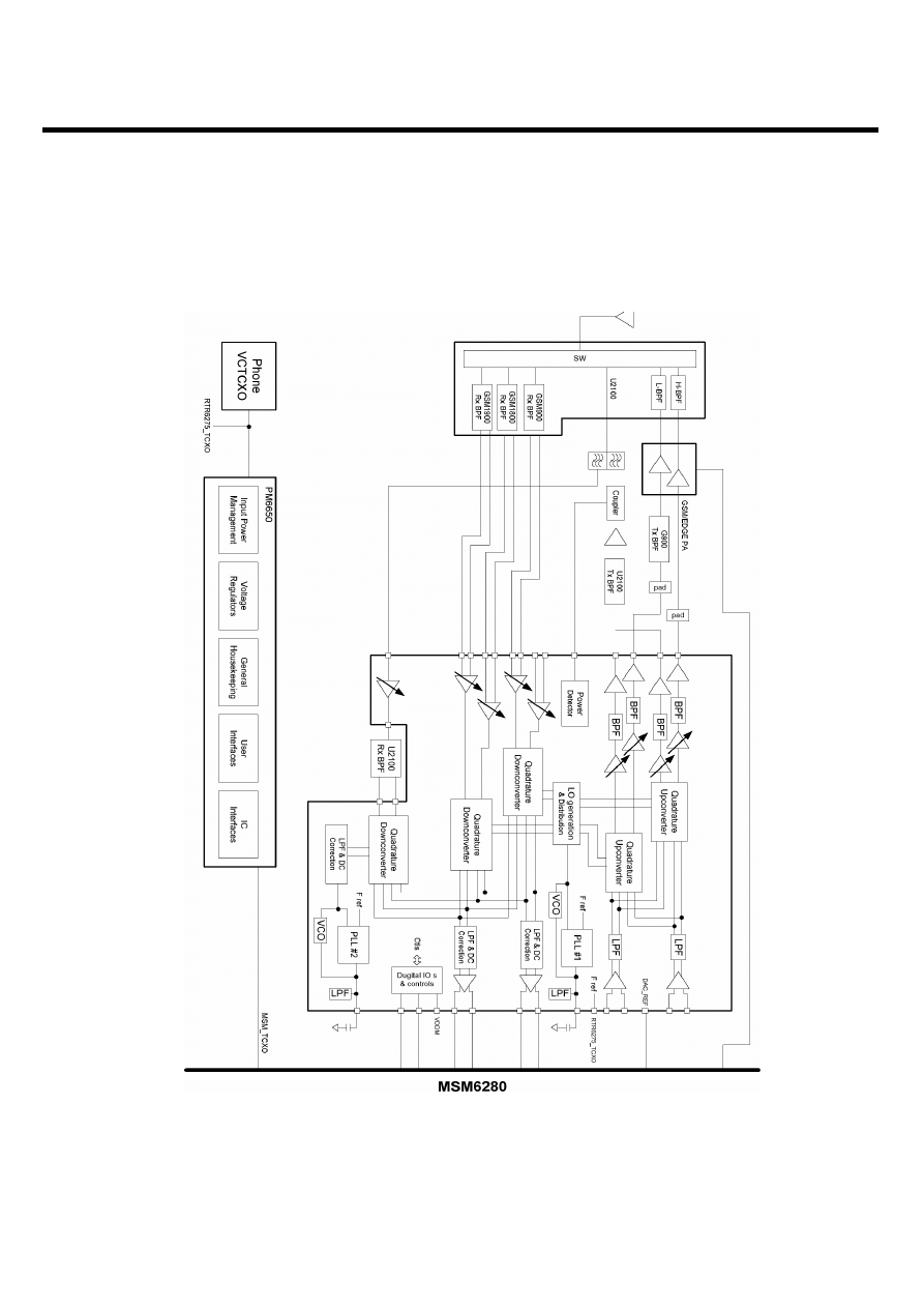
- 167 -
6. BLOCK DIAGRAM
6. BLOCK DIAGRAM
LGE Internal Use Only
Copyright © 2007 LG Electronics. Inc. All right reserved.
Only for training and service purposes
6.1 GSM & UMTS RF Block
[Figure 2.1] UMTS-2100 + EGSM-900/DCS-1800/PCS-1900 RF Functional Block Diagram
- 168 -
6. BLOCK DIAGRAM
LGE Internal Use Only
Copyright © 2007 LG Electronics. Inc. All right reserved.
Only for training and service purposes
[Table 2.1] RF Block Component
Block
Ref. Name
Part Name
Function
Comment
FL100
LSHS-M090UH
Front End Module
ASM+Rx Saw
SW100
KMS518
Test Connector
Calibration, etc
X100 TG-5010LH_19_2M
VCTCXO
19.2MHz
Common
U100
RTR6275
RF Transceiver IC
TRX
M800
LBRQ-2B43A
BT RF Transceiver
BT TRX
Bluetooth
FL103 SAYZ1G95EB0B00
Duplexer
TRX
FL102
EFCH2140TDE1
RX SAW Filter
RX
FL104
EFCH1950TDF1
TX SAW Filter
TX
U105 AWT6277R
TX PAM
TX
UMTS
U104 CP0402A1950DNTR
Coupler
TX
U101
TQM7M5003
TX Dual PAM
TX
GSM
FL101
EFCH897MTDB1
Tx SAW Filter
Tx
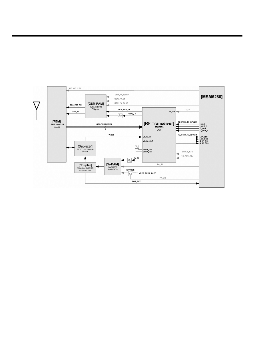
- 169 -
6. BLOCK DIAGRAM
LGE Internal Use Only
Copyright © 2007 LG Electronics. Inc. All right reserved.
Only for training and service purposes
6.2 Interface Diagram
[Figure 2.2] U990 Interface Diagram
- 170 -
6. BLOCK DIAGRAM
Main RF signal
Control signal
LGE Internal Use Only
Copyright © 2007 LG Electronics. Inc. All right reserved.
Only for training and service purposes
Main RF signal
Description
Comment
GSM 900 TX
GSM 900 TX RF Signal
DCS TX
DCS TX RF Signal
PCS TX
PCS TX RF Signal
W- TX
UMTS2100 TX RF Signal
GSM 900 RX
GSM 900 RX RF Signal
DCS RX
DCS RX RF Signal
PCS RX
PCS RX RF Signal
W- RX
UMTS2100 RX RF Signal
TX_I/Q
I/Q for Tx of RF
RX_I/Q
I/Q for Rx of RF
Control signal
Description
Comment
UMTS PA_CTL signal
PA_R1 UMTS Tx High/Low Power Control
PA_ON Power
Amp.
Enable
GSM PA_CTL signal
GSM_PA_BAND DCS or PCS /GSM Mode Selection
GSM_PA_EN Power Amp. Gain Control Enable
GSM_PA_RAMP Power Amp. Gain Control
RF Tranceiver_CTL signal
TX_ON RF Enable Signal
SSBDT_RTR Bidirectional
SSBI
Data
TX_AGC_ADJ UMTS Transmit Gain Control
FEM_CTL signal
ANT_SEL 0,1,2 Ant Switch Module Mode Selection
UMTS,
GSM900Tx/Rx,
DCS Tx/Rx,
PCS Tx/Rx
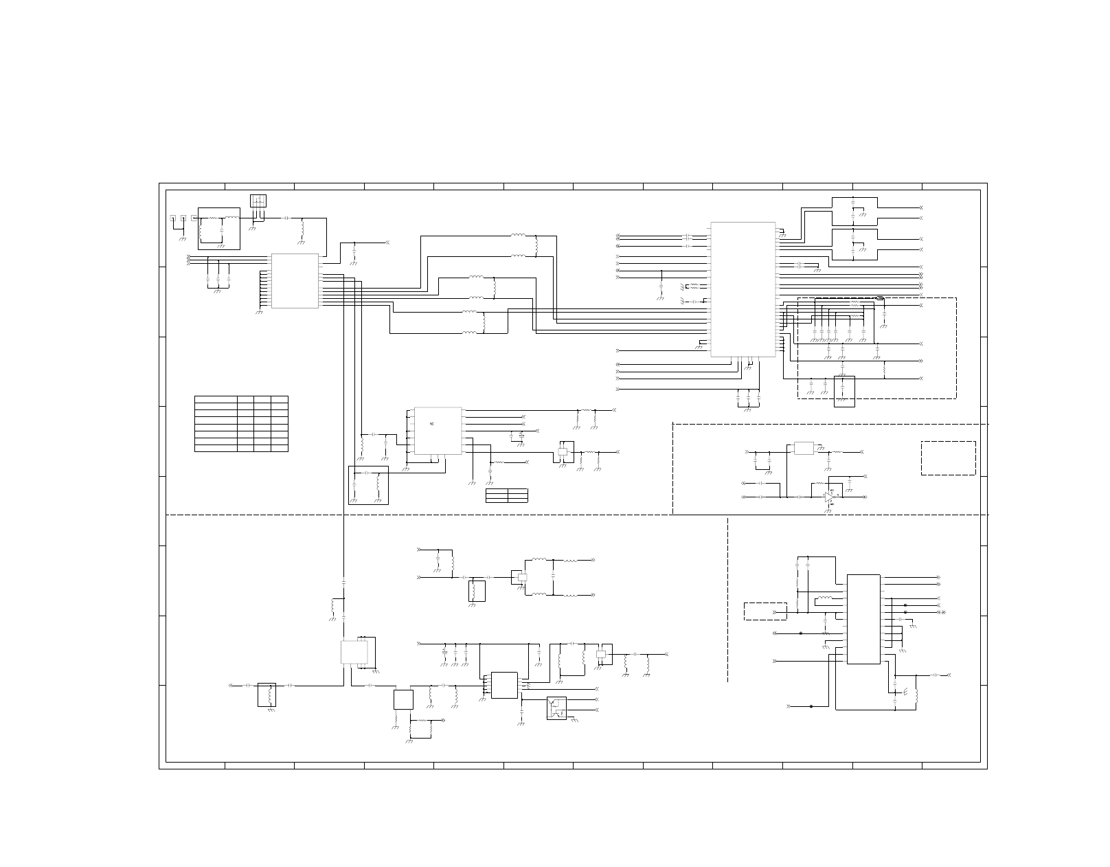
- 171 -
6
11
10
Thermistor circuit deleted
B
HIGH
D
8
F
4
WCDMA
GSM 850/GSM 900 TX
HIGH
H
MODE
D
WCDMA
ANTENNA SWITCH MODULE LOGIC
G
A
PQ
PQ
DCS
LOW
10
1
ANT_SEL1
ANT_SEL2
5
A
11
SMPS circuit for RF
20dB
HIGH
C
9
GSM 1900 RX
GSM_PA_BAND
GSM
(1%)
8
B
F
F
VTUNE-Connected directly to GND
C
C
LOW
LOW
D
LOW
5
4
6
11
12
4
LOW
9
2
HIGH
G
8 dB
11
GSM 1800/GSM 1900 TX
LOW
B
E
GSM
1
7
E
2
TCXO
10 dB
PCS
HIGH
9
12
6
GSM 900 RX
GSM 1800 RX
(1%)
HIGH
near to 48pin
G
10
3
HIGH
7
1
A
F
GSM
HIGH
H
3
D
5
H
ANT_SEL0
DCS/PCS
LOW
E
LOW
3
PQ
PQ
2
H
5
LOW
7
C
12
7
B
GSM 850 RX
LOW
HIGH
8
E
2
8 dB
HIGH
6
8
12
9
G
LOW
LOW
10
A
FM RADIO
Rev. 1.1
4
3
1
LOW
C138
NA
56p
C105
NA
33u
C135
C104
C165
1.2p
22p
C133
L125
1.2nH
0.1u
C139
15nH
L104
1nH
120
R119
0.1u
L118
C121
C149
0.1u
22p
C122
C147
1000p
C123
0.1u
1.5nH
C117
L114
47nH
L120
22p
100p
100ohm
R115
C163
C128
22p
VDDA5
15
16
VDDA6
19
VDDA7
VDDA8
20
28
VDDA9
VDDM
17
VTUNE1
5
18
VTUNE2
26
WLNA_IN
WLNA_OUT
29
35
WMIX_INN
WMIX_INP
34
7
TCXO
21
TEST
TX_IN
50
TX_IP
51
52
TX_QN
TX_QP
53
VCONTROL
56
4
VDDA1
VDDA10
41
45
VDDA11
VDDA12
47
48
VDDA13
VDDA14
49
6
VDDA2
VDDA3
8
9
VDDA4
GPCS_INN
37
36
GPCS_INP
HB_RF_OUT1
46
HB_RF_OUT2
44
43
LB_RF_OUT1
LB_RF_OUT2
42
PGND
57
40
PWD_DET_IN
24
RF_ON
13
RX_IN
RX_IP
12
RX_QN
11
10
RX_QP
R_BIAS1
3
R_BIAS2
27
SBDT
14
U100
CAL_INN
23
22
CAL_INP
54
DAC_REF
DCS_INN
39
38
DCS_INP
EGSM_INN
33
32
EGSM_INP
1
ENV_LNN
ENV_LNP
2
ENV_OUT
55
GCELL_INN
30
GCELL_INP
31
25
GND
47p
C109
RTR6275
100nH
L127
L121
0.01u
2.2nH
VCC
VCCVCO
A5
VDD
D1
VREFDIG
E3
C151
DGND1
D3
DGND2
FREQIN
C1
B2
INTX
ISS
D5
LO1
A3
LO2
A4
LOOPSW
A2
E4
MPXOUT
RFGND
C5
RFIN1
B6
C6
RFIN2
SWPORT
B1
D6
TMUTE
VAFL
E5
VAFR
E6
A6
U103
TEA5766UK
B5
AGND
C2
BUSEN
E2
CLOCK
A1
CPOUT
E1
DATA
D2
C160
22u
1000p
C145
120
R118
51
R124
L122
NA
100
R126
0.1u
C168
C150
2
4
5
3
1
56p
Q100
KRX102E
C162
0.01u
0.01u
C141
15nH
L123
5p
51
R114
C108
5.6nH
L103
1000p
C112
C153
ANT101
C115
56p
27p
47p
2
RFIN
RFOUT
8
VCC1
1
10
VCC2
4
VMODE
VREF
5
C172
AWT6277R
U105
GND1
3
GND2
6
7
GND3
9
GND4
GND5
11
C167
56p
91
R112
5.6p
C169
47p
C113
C124
0.1u
15nH
R117
2.2K
L107
0.1u
C119
L119
C142
0.75p
8p
C136
1nH
8200p
C148
C161
56p
SCDY0003403
50OHM
4
3
COUP
2
IN
1
OUT
TP103
C173
100p
U104
NA
L102
TP102
100p
3300p
C131
C111
R109
10
R123
1000p
C134
68
91
0.1u
R113
C129
1000p
C140
0.5p
C155
C159
8.2p
1u
C137
A
C
G1
G2
L113
KMS-518
SW100
14
GND6
GND7
16
17
GND8
7
GSM_IN
9
GSM_OUT
3
TX_EN
VBATT
4
12
VCC
VRAMP
6
4.7nH
TQM7M5003
U101
2
BS
DCS_PCS_IN
1
DCS_PCS_OUT
15
5
GND1
GND2
8
10
GND3
11
GND4
13
GND5
L109
22nH
X100
2
GND
OUT
3
VCC
4
VCONT
1
R107
2.7
2
G1
3
G2
5
G3
1
IN
4
O1
19.2MHz
EFCH897MTDB1
FL101
120p
C101
C154
56p
C152
3.9p
C127
100p
12
GND5
14
GND6
GND7
15
GND8
17
18
GND9
NC
7
PCS_RX1
22
PCS_RX2
21
25
PGND1
26
PGND2
8
UMTS_TX_RX
VC1
5
4
VC2
VC3
3
VDD
6
ANT
10
DCS_PCS_TX
13
DCS_RX1
20
19
DCS_RX2
EGSM_RX1
24
23
EGSM_RX2
EGSM_TX
16
1
GND1
2
GND2
GND3
9
11
GND4
15nH
FL100
LSHS-M090UH
L112
47p
C114
680
R101
1.8p
180p
C100
C170
C110
180p
C146
10p
L116
1nH
ANT100
L128
4.7nH
TP101
C157
0.1u
R120
C158
1u
100K
C107
12p
C116
180p
180p
C103
L124
3.3nH
L126
8.2nH
C171
56p
5.6nH
L105
R102
0
C125
1u
100K
R122
FL102
EFCH2140TDE1
G1
2
G2
5
IN
1
O1
3
O2
4
EFCH1950TDF1
FL104
G1
2
G2
3
G3
5
IN
1
O1
4
C126
22p
R125
100
L117
1.8nH
L115
1nH
NA
R103
68p
C143
0
L100
R100
12K
5.6nH
L106
TC7SH04FS
C130
22u
U102
1u
C164
C156
2.2p
TP100
22nH
L110
5.1
R104
C166
100p
C102
12nH
L101
4.7nH
22u
C118
FL103
ANT
2
1
GND1
GND2
4
8
GND3
GND4
9
GND5
6
GND6
3
7
RX
5
TX
SAYZY1G95EB0B00
68
R111
ANT102
C144
L111
22nH
1000p
0.01u
C132
C120
0.1u
10K
R121
L108
6p
C106
5.6nH
TX_AGC_ADJ
DAC_REF
WCDMA_MIX_IN_M
WLNA_OUT
RX_WCDMA_2100
VREG_MSMP_2.7V
VDD_RX
VREG_RF_SMPS
VREG_SYNTH_2.6V
VREG_RF_SMPS
TX_QP
TX_QM
TX_IP
TX_IM
RTR6275_TCXO
SSBDT_RTR
RX_QP
RX_QM
RX_IP
RX_IM
TX_ON
PWR_DET
VREG_RF_SMPS
ANT_SEL2
WCDMA_2100_TX_OUT
I2C_SDA
I2C_SCL
FM_INTX
SLEEP_CLK
GSM_PA_BAND
+VPWR
WCDMA_MIX_IN_P
PA_ON
VREG_TCXO_2.85V
+VPWR
WCDMA_2100_TX_OUT
DCS_PCS_TX
GSM_TX
DCS_PCS_TX
GSM_TX
PA_R1
WLNA_OUT
WCDMA_MIX_IN_M
WCDMA_MIX_IN_P
VDD_RX
ANT_SEL0
ANT_SEL1
TRK_LO_ADJ
VREG_TCXO_2.85V
TCXO_BT
VREG_BT_2.85V
TCXO_PM
RTR6275_TCXO
FM_ANT
VREG_MSMP_2.7V
VREG_MMC_3.0V
FM_BUSEN
FM_AUDIO_R
FM_AUDIO_L
RX_WCDMA_2100
PWR_DET
GSM_PA_RAMP
GSM_PA_EN
7. CIRCUIT DIAGRAM
LGE Internal Use Only
Copyright © 2007 LG Electronics. Inc. All right reserved.
Only for training and service purposes
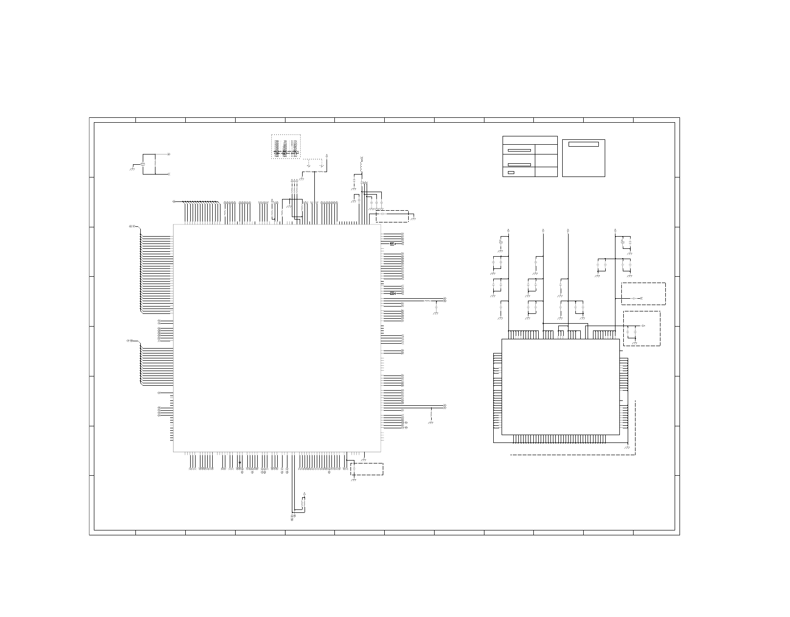
- 172 -
D12(VDDA1) and F12(DAC_REF)
D
E
10%
Place near
1
this pin can be grounded as in MSM6275
E
1
D
Near to B18 (VDD_PLL)
PMIC_AUXIN[1]
7
3
9
1
0
5
6
F
PMIC_AUXIN[2] - PA_THERM
2
B
8-bit, NAND boot
11
12
E
C
10
12
2
H
w18 (Analog VSS guard ring for CODEC)
MSM pin W18
G
7
0 0 0
6
MODE
( +/- 2500ppm for USB Peripheral )
G
Normal boot
BOOT_MODE3
0
( Default Pull-Down)
9
(CODEC VSS)
5
11
4
2
8
4
1
Trusted boot
(VDD_DAC_REF)
A
A
for VSS_THERMAL
MSM pin AD26
8
G
(CAD : 10uF=>Input MSMA_2.6V)
BOOT_MODE2 BOOT_MODE
10%
If you are not Qfuse (security),
B
C
8
12
B
D
A
B
5
H
E
Native, MSM JTAG
6
9
0 1
10
D
F
1 1
F
11
F
NOR boot
HKADC[4] - PCB_Rev_ADC
H
7
HKADC[0] - AMUX_OUT
HKADC[1] - VBATT_SENSE
HKADC[2] - HDET1
16-bit, NAND boot
4
3
7
2
10%
1
G
11
10
9
4
3
ADC
6
HKADC[3] - REMOTE_ADC
1%
Native, ARM JTAG
MODE2 MODE1 MODE0
Place near
(WCMDA 2100 PAM Enable)
3
5
C
(PLLOUT_TEST)
1
0 1 0
12
1%
2200p cap => place between
H
A
8
PCB_Rev_ADC
USB 48M CLK
X 0
HKADC[5] - VBATT_TEMP
C
0.01u
0.01u
C219
C220
C217
1000p
R201
470K
51
R207
C230
VREG_MSMP_2.7V
0.1u
4.7u
C239
0.1u
C228
C204
NA
VREG_MSMA_2.6V
R213
NA
VREG_MSMP_2.7V
0.01u
C214
2200p
C222
R205
51K
C215
0.1u
0.1u
VREG_MSMP_2.7V
C232
R202
150K
C238
0.1u
1M
R200
100K
R206
1000p
C226
48MHz
13
2
X200
ICRT20S48M0X514CR
33nF
C211
C223
0.01u
C216
0.1u
0.1u
VREG_MSME_1.8V
VREG_MSMP_2.7V
C235
C231
0.01u
1u
R210
0
C225
C221
0.01u
R209
NA
0.01u
VREG_MSMC_1.2V
C213
C236
0.1u
R211
2K
NA
R203
NA
C237
R204
51K
2.2K
R217
L200
100nH
TP200
R218
2.2K
VREG_MSMA_2.6V
VREG_MSMP_2.7V
0.01u
0.1u
C210
C229
100K
R208
1u
C234
NA
C203
C212
0.1u
1000p
C218
1000p
0
R215
C227
C224
C200
1u
VREG_MSMP_2.7V
10p
A24
VSS_DIG_9
VSS_PAD1_0
F1
VSS_PAD1_1
K1
M1
VSS_PAD1_2
R1
VSS_PAD1_3
U1
VSS_PAD1_4
VSS_PAD2_0
AF6
AF11
VSS_PAD2_1
AF15
VSS_PAD2_2
VSS_PAD3_0
R26
B17
VSS_PAD3_1
VSS_PAD3_2
A15
VSS_PAD3_3
A9
VREG_MSME_1.8V
VSSA7
V26
W16
VSSA8
W18
VSSA9
VSS_DIG
AC23
VSS_DIG_0
C1
VSS_DIG_1
H1
A14
VSS_DIG_10
VSS_DIG_11
A11
VSS_DIG_12
A5
W1
VSS_DIG_2
VSS_DIG_3
AC1
VSS_DIG_4
AF8
VSS_DIG_5
AF16
VSS_DIG_6
T26
G26
VSS_DIG_7
D26
VSS_DIG_8
VSS7
B25
B26
VSS8
VSS9
D4
A18
VSSA1
VSSA10
W26
VSSA11
AB26
AC16
VSSA12
VSSA13
AC26
AD25
VSSA14
AF23
VSSA15
AF24
VSSA16
VSSA2
A21
D13
VSSA3
D19
VSSA4
VSSA5
P26
VSSA6
U19
VSS36
T16
W8
VSS37
W19
VSS38
VSS39
AA6
A26
VSS4
AC4
VSS41
VSS43
AE1
AE2
VSS44
VSS45
AE25
AE26
VSS46
AF1
VSS47
AF2
VSS48
VSS49
AF25
VSS5
B1
AF26
VSS50
B2
VSS6
M14
VSS21
VSS22
M15
N12
VSS23
VSS24
N13
N14
VSS25
VSS26
N15
P12
VSS27
VSS28
P13
P14
VSS29
VSS3
A25
P15
VSS30
R12
VSS31
VSS32
R13
R14
VSS33
VSS34
R15
T11
VSS35
VDD_PAD3_3
B9
VDD_PAD4_0
A3
B18
VDD_PLL
VSS1
A1
D23
VSS10
F6
VSS11
VSS12
F21
VSS13
H8
H19
VSS14
K10
VSS15
L11
VSS16
L16
VSS17
VSS18
M11
M12
VSS19
A2
VSS2
VSS20
M13
T25
VDD_DIG_6
VDD_DIG_7
G25
VDD_DIG_8
D25
B24
VDD_DIG_9
VDD_MDDI
B21
F2
VDD_PAD1_0
K2
VDD_PAD1_1
VDD_PAD1_2
M2
VDD_PAD1_3
R2
VDD_PAD1_4
U2
AE6
VDD_PAD2_0
AE11
VDD_PAD2_1
AE15
VDD_PAD2_2
R25
VDD_PAD3_0
K25
VDD_PAD3_1
VDD_PAD3_2
B15
U25
VDDA3
VDDA4
U26
VDDA5
Y26
VDDA6
AA26
AE23
VDDA7
VDDA8
AE24
VDDA9
AA16
C2
VDD_DIG_0
H2
VDD_DIG_1
B14
VDD_DIG_10
B11
VDD_DIG_11
VDD_DIG_12
B5
VDD_DIG_2
W2
VDD_DIG_3
AC2
VDD_DIG_4
AE8
VDD_DIG_5
AE16
U200-2
MSM6280_B
AA21
NC
C26
RESERVED
VDDA1
D12
AF17
VDDA10
VDDA2
P23
R16
VDD_EF_USE
AE17
WDOG_EN
WDOG_STB_SBCK1_GPIO0
H25
U8
WE1_N_SDRAM1_WE_N
WE2_N
AF4
XMEM1_CS_N0
W6
AA1
XMEM1_CS_N1_GPIO76
Y4
XMEM1_CS_N2_SDRAM1_CS_N0
XMEM1_CS_N3_SDRAM1_CS_N1_GPIO77
Y6
XMEM1_HWAIT_N
AA2
XMEM1_LWAIT_N_SDRAM1_CAS_N
K8
XMEM2_CS_N0
W14
XMEM2_CS_N1
AC15
XMEM2_CS_N2_GPIO35
W15
AA15
XMEM2_CS_N3_GPIO36
G6
UART2_CTS_N_GPIO90
H6
UART2_DP_RX_DATA_GPIO89
UART2_DP_TX_DATA_GPIO88
E4
UART2_RFR_N_GPIO91
F4
L23
UART3_CTS_N_GPIO86
M21
UART3_DP_RX_DATA_GPIO85
UART3_DP_TX_DATA_GPIO84
M19
L25
UART3_RFR_N_GPIO87
UB1_N_SDRAM1_DQM1
M6
UB2_N
AF10
USB_DAT_VP
N26
N25
USB_OE_TP_N
USB_RX_DATA_GPIO29
N19
USB_SE0_VM
N23
USB_XTAL48_IN
A10
B10
USB_XTAL48_OUT
SYNTH1_GPIO41
H23
B6
SYNTH2_GPIO65
TCK
D16
TCXO
D18
TCXO_EN_GPIO94
F19
TDI
D15
TDO
A17
TMS
F15
TRK_LO_ADJ
L13
H15
TRST_N
H13
TX_AGC_ADJ
TX_ON_GRFC10
H12
P16
UART1_CTS_N_GPIO97
UART1_DP_RX_DATA_GPIO96
M23
UART1_DP_TX_DATA_GPIO95
L26
P21
UART1_RFR_N_PA_POWER_CTL_M_GPIO98
K6
SDRAM1_D11
J1
SDRAM1_D12
SDRAM1_D13
K4
L8
SDRAM1_D14
SDRAM1_D15
L6
SDRAM1_D2
AB2
D1
SDRAM1_D3
AB4
SDRAM1_D4
J6
SDRAM1_D5
G2
SDRAM1_D6
SDRAM1_D7
H4
P4
SDRAM1_D8
SDRAM1_D9
J4
A16
SLEEP_XTAL_IN
B16
SLEEP_XTAL_OUT
F18
SYNTH0_GP_PDM0_GPIO92
RINGER_GPIO18
L19
G1
ROM1_ADV_N_SDRAM1_RAS_N
AB1
ROM1_CLK_SDRAM1_CLK
RTCK
H16
L21
SBCK
J23
SBDT
F26
SBDT1_GPIO1
H26
SBST
SBST1_GPIO93
H18
SDCC_DAT1_GPIO99
F25
M25
SDCC_DAT2_GPIO100
SDCC_DAT3_GPIO101
M26
N4
SDRAM1_CLK_EN
E2
SDRAM1_D0
D2
SDRAM1_D1
J2
SDRAM1_D10
T21
MODE2
T14
NAND2_FLASH_READY_GPIO33
OE1_N
V2
AF7
OE2_N
PA_ON0
F17
PA_ON1_GPIO2
H11
P25
PA_POWER_CTL
AA25
Q_IM_CH0
Q_IM_CH1
W23
Y25
Q_IP_CH0
Q_IP_CH1
V23
B12
Q_OUT
A12
Q_OUT_N
RESIN_N
F13
RESOUT_N
F11
AA4
RESOUT_N_EBI1
MDDIH_DATN
B19
B20
MDDIH_DATP
MDDIH_STBN
A19
A20
MDDIH_STBP
MDP_VSYNC_PRIMARY_GPIO105
AD2
AE3
MDP_VSYNC_SECONDA_GPIO104
MIC1N
AF20
MIC1P
AE20
AF21
MIC2N
AF22
MIC2P
MICBIAS
T15
M16
MMC_CLK_SDCC_CLK_GPIO31
MMC_CMD_GPIO30
H14
L14
MMC_DATA_SDCC_DAT0_GPIO32
MODE0
Y23
MODE1
U23
KEYSENSE3_N_GPIO47
R23
U21
KEYSENSE4_N_GPIO48
LB1_N_SDRAM1_DQM0
L2
LB2_N_A2_0
AE10
LCD_CS_N_GPIO38
AF14
AE13
LCD_EN_GPIO37
LINE_L_IN
AC21
AC22
LINE_L_IP
AC18
LINE_ON
LINE_OP
AC17
AC20
LINE_R_IN
LINE_R_IP
AC19
MDDIC_DATN
A23
A22
MDDIC_DATP
MDDIC_STBN
B23
MDDIC_STBP
B22
Y21
HKAIN4
HKAIN5
AB23
HPH_L
W17
AA17
HPH_R
HPH_VREF
AA19
N16
I2C_SCL_GPIO27
K21
I2C_SDA_GPIO26
AB25
I_IM_CH0
V25
I_IM_CH1
AC25
I_IP_CH0
I_IP_CH1
W25
I_OUT
B13
I_OUT_N
A13
R21
KEYSENSE0_N_GPIO62
KEYSENSE1_N_GPIO63
P19
KEYSENSE2_N_GPIO46
D14
D17
GP_PDM2_PA_RAN_GE1
B8
GRFC0_GPIO3
A8
GRFC1_AUX_SBDT_GPIO4
D9
GRFC2_GPIO5
GRFC3_GPIO6
F10
GRFC4_AUX_SBCK_GPIO7
H10
D11
GRFC5_AUX_SBST_GPIO8
GRFC7_GPIO10
T23
B4
GRFC8_GPIO11
D5
GRFC9_GPIO12
GRFX6_GPIO9
T19
GSM_PA_DAC_REF
AD26
HKAIN0
V21
HKAIN1
AA23
W21
HKAIN2
HKAIN3
V19
F9
GPIO49
GPIO50
B7
GPIO51
A7
GPIO52
D10
L12
GPIO53
F14
GPIO64
F8
GPIO66
GPIO_67
U6
V4
GPIO_68
GPIO_69
R11
GPIO_70
E1
Y1
GPIO_71
GPIO_72
Y2
GPIO_73
V6
W4
GPIO_74
GP_PDM1_PA_RAN_GE0
H17
D2_6
AF5
D2_7
AC7
D2_8
AA8
D2_9
W9
F12
DAC_REF
EAR1ON
AE18
EAR1OP
AF18
GPIO17
K26
G21
GPIO19
A6
GPIO28
GPIO39
F7
GPIO40
D6
D7
GPIO42
H9
GPIO43
GPIO44
D8
A4
GPIO45
CAMIF_HSYNC_GPIO15
E23
CAMIF_PCLK_GPIO82
K23
CAMIF_VSYNC_GPIO16
B3
CCOMP
AA20
D2_0
AC5
AF3
D2_1
AC8
D2_10
AE7
D2_11
D2_12
AA9
W10
D2_13
D2_14
AC9
D2_15
AA10
D2_2
AE4
AC6
D2_3
AE5
D2_4
AA7
D2_5
R19
BT_DATA_GPIO20
E26
BT_SBCK_GPIO23
BT_SBDT_GPIO22
E25
F23
BT_SBST_GPIO24
BT_TX_RX_N_GPIO21
H21
CAMCLK_PO_GP_MN_GPIO13
J21
CAMIF_DATA0_GPIO83
J25
J26
CAMIF_DATA1_GPIO81
CAMIF_DATA2_AUX_TRST_N_GPIO54
D21
CAMIF_DATA3_AUX_TCK_GPIO55
C25
CAMIF_DATA4_AUX_TMS_GPIO56
D22
J19
CAMIF_DATA5_AUX_TDI_GPIO57
CAMIF_DATA6_AUX_TDO_GPIO58
L15
CAMIF_DATA7_GPIO59
D20
F16
CAMIF_DATA8_GPIO60
F20
CAMIF_DATA9_GPIO61
AA11
A2_5
A2_6
AC11
T12
A2_7
W12
A2_8
A2_9
AA12
AF19
AUXIN
AE19
AUXIP
AUXOUT
AA18
AUX_PCM_CLK_GRFC14_GPIO80
K19
N21
AUX_PCM_DIN_GRFC13_GPIO14
G4
AUX_PCM_DOUT_GRFC12_GPIO103
AUX_PCM_SYNC_GRFC11_GPIO102
J8
AE21
BOOT_MODE
BOOT_MODE2
AE22
AD1
BOOT_MODE3
G23
BT_CLK_GPIO25
N1
A1_9
AE9
A2_1
AC12
A2_10
A2_11
AE12
A2_12
AF12
AA13
A2_13
A2_14
AC13
A2_15
W13
A2_16
AE14
AC14
A2_17
A2_18
T13
A2_19
AA14
AF9
A2_2
AF13
A2_20_GPIO34
A2_3
W11
AC10
A2_4
T1
A1_17
A1_18
T2
R8
A1_19
L4
A1_2
T4
A1_20
A1_21
T6
T8
A1_22
U4
A1_23_SDRAM1_DQM2_GPIO78
V1
A1_24_GPIO79
V8
A1_25_SDRAM1_DQM3_GPIO75
M8
A1_3
M4
A1_4
A1_5
N11
N8
A1_6
A1_7
N6
A1_8
N2
MSM6280_A
L1
A1_1
P1
A1_10
A1_11
P2
A1_12
P6
P8
A1_13
A1_14
P11
R4
A1_15
A1_16
R6
C233
10u
U200-1
VGA_CAM_PWR_EN
MMP_INT_N
HP_R
HP_L
MMP_LCD_BYPASS_CS_N
RMT_INT
RMT_ADC
WHEEL_SW_R
WHEEL_SW_L
CAM_MCLK
LCD_RESET_N
VGA_CAM_RESET_N
CAM_SELECT_N
MICROSD_DETECT
UART_TXD
UART_RXD
VGA_CAM_PWDN
BT_DATA
BT_SBDT
BT_SBCK
BT_SBST
BT_TX_RX_N
BT_CLK
TOUCH_I2C_SCL
TOUCH_PENIRQ_N
MMP_HPCM_FSYNC
LCD_LDO_EN
MMP_HPCM_DI
MMP_HPCM_CLK
MMP_RESET_IN_N
MMP_PWR_EN
CODEC_I2C_SCL
CODEC_I2C_SDA
WM_EN
MMP_HPCM_DO
RX_IM
RX_IP
RX_QM
RX_QP
DAC_REF
PA_ON
TCXO_EN
TRK_LO_ADJ
TX_AGC_ADJ
LIN_INVERTER
HOOK_SENSE_N
LCD_VSYNC_OUT
LCD_IF_MODE
EBI2_ADDR[13]
EBI2_ADDR[14]
EBI2_ADDR[12]
EBI2_ADDR[11]
EAR_SENSE_N
LCD_MAKER_ID
TOUCH_I2C_SDA
MSM_MICROSD_DATA[3]
MSM_MICROSD_DATA[2]
MSM_MICROSD_DATA[1]
CAM_MODE1_N
CAM_MODE3_N
CAM_MODE2_N
MMC_SELECT_N
HP_AMP_EN
USB_XTAL_OUT
RESOUT_N
RESET_IN_N
MIC1P
MIC1N
MIC2P
AMUX_OUT
VBAT_TEMP
VBAT_SENSE
RCV+
RCV-
MICBIAS
SPK_L
SPK_R
TX_QM
TX_IM
GSM_PA_EN
TX_QP
TX_IP
ANT_SEL2
GSM_PA_BAND
FM_INTX
TX_ON
PA_R1
ANT_SEL0
ANT_SEL1
LIN_PWM_FREQ
GSM_PA_PWR_CTL_REF
GSM_PA_RAMP
SDRAM_ADDR[0:14]
SDRAM_ADDR[0]
SDRAM_ADDR[1]
SDRAM_ADDR[2]
SDRAM_ADDR[3]
SDRAM_ADDR[4]
SDRAM_ADDR[5]
SDRAM_ADDR[6]
SDRAM_ADDR[7]
SDRAM_ADDR[8]
SDRAM_ADDR[9]
SDRAM_ADDR[10]
SDRAM_ADDR[11]
SDRAM_ADDR[12]
SDRAM_ADDR[13]
SDRAM_ADDR[14]
SDRAM_CLK
SDRAM_RAS_N
SDRAM_CLK_EN
SDRAM_CAS_N
SDRAM_DQM[0]
SDRAM_DQM[1]
SDRAM_DQM[2]
SDRAM_WE_N
SDRAM_DQM[3]
SDRAM_CS_N
USB_XTAL_IN
SLEEP_CLK
BUFF_TCXO
USIM_DATA
KEY_COL[1]
PM_INT_N
PS_HOLD
USIM_CLK
USIM_RST_N
KEY_COL[0]
SSBDT_RTR
I2C_SCL
I2C_SDA
SSBDT_PM
USB_SE0
USB_DAT
KEY_ROW[2]
KEY_ROW[1]
KEY_ROW[0]
USB_OE_N
MSM_MICROSD_CMD
MSM_MICROSD_DATA[0]
MSM_MICROSD_CLK
MMP_CAM_DATA[6]
MMP_CAM_DATA[2]
MMP_CAM_VSYNC
MMP_CAM_DATA[4]
MMP_CAM_DATA[1]
LCD_BL_CTRL
MMP_CAM_DATA[7]
MMP_CAM_DATA[5]
MMP_CAM_DATA[0]
MMP_CAM_PCLK
MMP_CAM_HSYNC
MMP_CAM_DATA[3]
SDRAM_DATA[7]
SDRAM_DATA[6]
SDRAM_DATA[5]
SDRAM_DATA[4]
SDRAM_DATA[3]
SDRAM_DATA[2]
SDRAM_DATA[1]
SDRAM_DATA[0]
EBI2_DATA[0:15]
EBI2_DATA[15]
EBI2_DATA[14]
EBI2_DATA[13]
EBI2_DATA[12]
EBI2_DATA[11]
EBI2_DATA[10]
EBI2_DATA[9]
EBI2_DATA[8]
EBI2_DATA[7]
EBI2_DATA[6]
EBI2_DATA[5]
EBI2_DATA[4]
EBI2_DATA[3]
EBI2_DATA[2]
EBI2_DATA[1]
EBI2_DATA[0]
NAND_ALE
NAND_READY
NAND_CLE
EBI2_WE_N
EBI2_OE_N
NAND_CS_N
MMP_CS_N
USB_XTAL_OUT
USB_XTAL_IN
DAC_REF
FM_BUSEN
USB_SELECT_N
LIN_PWM_MAG
LIN_MOTOR_EN
SDRAM_DATA[0:31]
SDRAM_DATA[31]
SDRAM_DATA[30]
SDRAM_DATA[29]
SDRAM_DATA[28]
SDRAM_DATA[27]
SDRAM_DATA[26]
SDRAM_DATA[25]
SDRAM_DATA[24]
SDRAM_DATA[23]
SDRAM_DATA[22]
SDRAM_DATA[21]
SDRAM_DATA[20]
SDRAM_DATA[19]
SDRAM_DATA[18]
SDRAM_DATA[17]
SDRAM_DATA[16]
SDRAM_DATA[15]
SDRAM_DATA[14]
SDRAM_DATA[13]
SDRAM_DATA[12]
SDRAM_DATA[11]
SDRAM_DATA[10]
SDRAM_DATA[9]
SDRAM_DATA[8]
7. CIRCUIT DIAGRAM
LGE Internal Use Only
Copyright © 2007 LG Electronics. Inc. All right reserved.
Only for training and service purposes
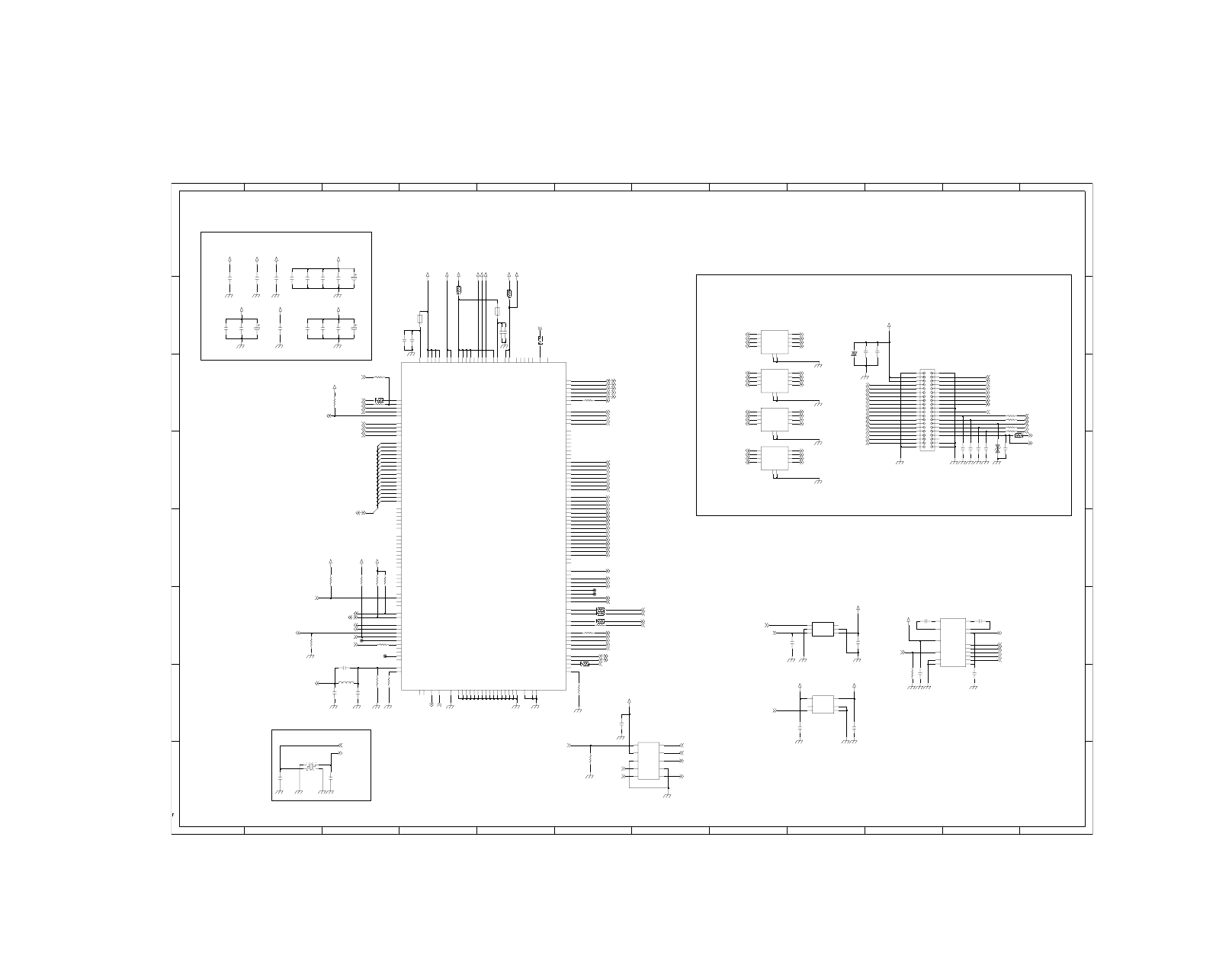
- 173 -
4
LCD BACKLIGHT CHARGE PUMP
8
E
G
3.4K
7
H
5
F
H
12
9
LCD INTERFACE
6
G
12
C
3
4
A
11
7
9
10
1
8
F
H
3
E
1
11
9
SWITCH FOR USB2.0
7
D
8
E
10
D
F
1
2
OTP Program Pin
392ohm 1%
3
A
7
2
10
B
G
B
1
6
D
F
2
ENBY0036001
LCD connector change : 35pin ZIF -> 40pin BTB
6
11
5
9
C
27Mhz XTAL
3
4
A
1%
12
LCD LDO
5
12
8
D
1.0T, Socket
C
2
A
E
H
5
11
G
150mA
6
4
B
GB042-40S-H10-E3000
B
C
10
C310
0.1u
330p
C335
7
INOUT_B3
INOUT_B4
6
0
R308
FL301 ICVE10184E150R500FR
G1
5
G2
10
INOUT_A1
1
2
INOUT_A2
INOUT_A3
3
4
INOUT_A4
9
INOUT_B1
INOUT_B2
8
+VPWR
C313
0.1u
R327
NA
C328
1u
100K
R336
7
C2+
8
C2-
D1
11
12
D2
D3
13
D4
14
D5
1
D6
2
3
EN_SET
GND
10
IN
9
6
OUTCP
15
PGND
U301
AAT3169IFO-T1
4
C1+
C1-
5
MMP_VDD_1.9V
C322
22p
R333
NA
C323
22p
10K
R319
VREG_MSMP_2.7V
LCD_VDD_2.8V
FB301
1u
1K
R321
C317
0.1u
M9
VIDP
VMCLK
P12
P10
VPCLK
VVS
K12
H14
XTALIN
XTALOUT
J14
MMP_VDD_USB_3.3V
C306
M12
VHREF
P8
VIDA
N8
VIDB
P9
VIDC
VIDD
M10
N10
VIDE
N9
VIDF
VIDG
N11
VIDH
P11
N12
VIDI
N7
VIDJ
VIDK
L8
P13
VIDL
L9
VIDM
VIDN
N13
VIDO
M11
VDDCORE1
D8
VDDCORE2
F4
VDDCORE3
J11
VDDCORE4
L7
VDDQ1
L6
VDDQ2
D7
VDD_CIS
M8
VDD_GENERAL
H4
D9
VDD_HOST
D6
VDD_LCD
G2
VDD_MMC
K10
VDD_NAND
D10
VDD_PMU
G4
VDD_SERIAL
E13
VENBYPIN
VENBYPOUT
E11
E12
TDI
D13
TDO
F14
TEST
E14
TMS
D14
TRSTN
TVDATA
G14
TVREF
F13
UARTCTS
L1
UARTRTS
M1
UARTRX
N3
UARTTX
M4
UDN
P4
P3
UDP
P6
UID
URSET
M7
J4
UVBUS
NWEN
K13
RESETN
G13
SCL
N14
SCLK
G1
H2
SCMD
SDA
P14
SDAT0
F1
SDAT1
F2
SDAT2
E5
F3
SDAT3
SPICLK
N2
K3
SPICS
SPIDI
J3
SPIDO
L2
G3
SWP
D11
TCK
E3
LVS
C4
LWRN
NALE
M13
L12
NCLE
NCSN
L13
L14
ND0
L10
ND1
ND15
K11
ND2
J12
H12
ND3
ND4
K14
G12
ND5
J13
ND6
H13
ND7
NRBN
M14
NREN
L11
LD12
C1
LD13
C2
C5
LD14
LD15
C6
D3
LD16
LD17
D1
B6
LD2
LD3
B4
LD4
A4
C3
LD5
A3
LD6
LD7
A2
A1
LD8
LD9
B2
E4
LHS
LRDN
D5
HGINTN
A7
HPCMCLK
H3
HPCMDI
J1
J2
HPCMDO
H1
HPCMFS
B7
HRDN
HWRN
B9
D4
LA0
LACT
E2
LCK
E1
A6
LCS0N
LCS1N
D2
LD0
B5
A5
LD1
LD10
B1
B3
LD11
HD0
D12
HD1
C10
B12
HD10
A12
HD11
HD12
B11
A11
HD13
HD14
C9
B10
HD15
HD2
C12
C13
HD3
C14
HD4
HD5
B14
HD6
C11
B13
HD7
A14
HD8
HD9
A13
GPIO0
P2
M3
GPIO1
GPIO2
P7
N1
GPIO3
GPIO4
P1
GPIO5
M5
N6
GPIO6
GPIO7
M6
P5
GPIO8
N5
GPIO9
A10
HA11
HA12
A9
C8
HA13
C7
HA14
HCS0N
B8
HCS1N
A8
F6
GND1
GND10
H7
GND11
H8
GND12
H9
GND13
J6
J7
GND14
J8
GND15
GND16
J9
F7
GND2
F8
GND3
GND4
F9
GND5
G6
G7
GND6
GND7
G8
G9
GND8
H6
GND9
ABCLK
M2
ADI
L3
K1
ADO
AFS
K2
L5
AGND_USBC
K5
AGND_USBT
F12
AGND_VDAC
AMCLK
N4
AVDD_PLL
E10
L4
AVDD_USBC
AVDD_USBT
K4
H11
AVDD_VDACI
G11
AVDD_VDACP
AVSS_PLL
F11
10p
U302
ZR3453
22p
C315
C331
R315
51
C316
0.1u
100K
100K
R320
R345
X300
FA-238_27MHz_9PF
1
2
3
4
CAM_VDD_IO_2.7V
27MHz
C318
0.1u
0.1u
C314
22p
C304
+VPWR
C325
0.1u
R329
33
1u
C337
C329
1u
VA300
ICVN0505X150FR
0
R300
25
26
27
28
29
CAM_VDD_IO_2.7V
9
21
30
31
32
33
34
35
36
37
38
39
22
40
23
24
12
13
14
15
16
17
18
19
2
20
3
4
5
6
7
8
CN300
1
10
11
VA301
R340
3.3K
CAM_VDD_IO_2.7V
10p
C311
TP303
C339
8p
CAM_VDD_IO_2.7V
51
R314
R339
390
NA
VREG_MMC_3.0V
C320
C333
1u
C327
1u
1u
TP302
LCD_VDD_2.8V
C330
VREG_MMC_3.0V
C326
22p
C307
10p
C305
0.1u
10K
R310
U304
D+
3
D-
5
GND
4
1
HSD1+
7
HSD1-
2
HSD2+
HSD2-
6
SEL
10
9
VCC
8
_OE
0.1u
FSUSB30UMX
C312
1u
MMP_VDD_1.9V
G2
1
INOUT_A1
INOUT_A2
2
3
INOUT_A3
INOUT_A4
4
INOUT_B1
9
8
INOUT_B2
INOUT_B3
7
6
INOUT_B4
MMP_VDD_CORE_1.0V
C338
ICVE10184E150R500FR
FL303
5
G1
10
R311
0
TP301
NA
R313
CAM_VDD_IO_2.7V
51
R316
330p
C334
R318
0
10u
100K
TP300
C308
R331
R312
33
0.1u
VREG_MSMP_2.7V
C303
FB300
0.01u
C336
5
G1
10
G2
1
INOUT_A1
INOUT_A2
2
3
INOUT_A3
INOUT_A4
4
INOUT_B1
9
8
INOUT_B2
INOUT_B3
7
6
INOUT_B4
VREG_USB_3.3V
BGND
6
GND
2
5
SEL
1
STBY
3
VIN
4
VOUT
ICVE10184E150R500FR
FL300
U300
BH28PB1WHFV
NA
R309
51
R317
VREG_MSMP_2.7V
1
3
VOUT
+VPWR
R1114D191D-TR-F
U303
CE
6
2
GND1
5
GND2
4
NC
VDD
LCD_VDD_2.8V
R338
75
0
R325
MMP_VDD_1.9V
VREG_USB_3.3V
R335
0
0
R326
22p
C324
0
C301
R301
0.1u
0.1u
R324
0
C321
10u
C300
8p
C340
6
R322
1K
FL302 ICVE10184E150R500FR
G1
5
G2
10
INOUT_A1
1
2
INOUT_A2
INOUT_A3
3
4
INOUT_A4
9
INOUT_B1
INOUT_B2
8
7
INOUT_B3
INOUT_B4
1u
C332
10u
C309
MMP_VDD_CORE_1.0V
C302
0.1u
2.2uH
L300
1u
LCD_VDD_2.8V
MMP_RESET_IN_N
MMP_HPCM_DI
MMP_HPCM_CLK
MMP_HPCM_FSYNC
MMP_HPCM_DO
MMP_A_MCLK
WLED_1
MMP_CAM_INT
MMP_STROBE_READY
MMP_PWR_EN
C319
USB_SELECT_N
MMP_CS_N
LCD_VSYNC_OUT
MMP_CAM_MCLK
MMP_LCD_CS_N
MMP_LCD_ADS
MMP_LCD_RD_N
MMP_LCD_WE_N
LCD_MAKER_ID
WLED_2
WLED_3
WLED_4
WLED_5
LCD_BL_CTRL
WLED_PWR
+VPWR
LCD_LDO_EN
MMP_LCD_WE_N
MMP_LCD_VSYNC_OUT
WLED_PWR
WLED_2
WLED_4
WLED_5
MMP_INT_N
MMP_I2C_SDA
MMP_I2C_SCL
MMP_STROBE_CHARGE
MMP_CAM_HSYNC
MMP_ADI_ADCDAT
MMP_ADO_DACDAT
MMP_A_BCLK
MMP_A_LRCLK
MMP_LCD_VSYNC_IN
MMP_LCD_VSYNC_OUT
MMP_LCD_VSYNC_IN
MMP_LCD_BYPASS_CS_N
MICROSD_DETECT
MSM_USB_D-
MMP_USB_D-
USB_D+
USB_D-
MSM_USB_D+
MMP_USB_D+
TV_OUT
MMP_CAM_RESET_N
MMP_LCD_DATA[15]
NAND_ALE
MMP_CAM_PCLK
LCD_IF_MODE
LCD_DATA[0]
LCD_DATA[1]
LCD_DATA[2]
LCD_DATA[3]
LCD_DATA[4]
LCD_DATA[5]
LCD_DATA[6]
LCD_DATA[7]
LCD_DATA[14]
LCD_DATA[15]
LCD_DATA[8]
LCD_DATA[9]
LCD_DATA[10]
LCD_DATA[11]
LCD_DATA[12]
LCD_DATA[13]
WLED_1
WLED_3
MMP_LCD_ADS
MMP_LCD_CS_N
LCD_RESET_N
MMP_LCD_RD_N
MMP_LCD_DATA[9]
MMP_LCD_DATA[10]
MMP_LCD_DATA[11]
MMP_LCD_DATA[12]
MMP_LCD_DATA[13]
MMP_LCD_DATA[14]
MMP_LCD_DATA[15]
MMP_CAM_VSYNC
MMP_CAM_DATA[7]
MMP_CAM_DATA[6]
MMP_CAM_DATA[5]
MMP_CAM_DATA[4]
MMP_CAM_DATA[3]
MMP_CAM_DATA[2]
MMP_CAM_DATA[1]
MMP_CAM_DATA[0]
MMP_CAM_PWR_EN
MMP_MICROSD_CLK
MMP_MICROSD_DATA[3]
MMP_MICROSD_DATA[2]
MMP_MICROSD_DATA[1]
MMP_MICROSD_DATA[0]
MMP_XTAL_IN
MMP_XTAL_OUT
MMP_XTAL_IN
MMP_XTAL_OUT
MMP_USB_D+
MMP_USB_D-
VREG_5V
LCD_DATA[12]
LCD_DATA[13]
LCD_DATA[14]
LCD_DATA[15]
EBI2_ADDR[11]
EBI2_ADDR[13]
EBI2_ADDR[14]
MMP_MICROSD_CMD
MMP_LCD_DATA[0]
MMP_LCD_DATA[1]
MMP_LCD_DATA[2]
MMP_LCD_DATA[3]
MMP_LCD_DATA[4]
MMP_LCD_DATA[5]
MMP_LCD_DATA[6]
MMP_LCD_DATA[7]
MMP_LCD_DATA[8]
MMP_LCD_DATA[9]
MMP_LCD_DATA[10]
MMP_LCD_DATA[11]
MMP_LCD_DATA[12]
MMP_LCD_DATA[13]
MMP_LCD_DATA[14]
MMP_LCD_DATA[0]
MMP_LCD_DATA[1]
MMP_LCD_DATA[2]
MMP_LCD_DATA[3]
MMP_LCD_DATA[4]
MMP_LCD_DATA[5]
MMP_LCD_DATA[6]
MMP_LCD_DATA[7]
MMP_LCD_DATA[8]
EBI2_DATA[0:15]
EBI2_DATA[15]
EBI2_DATA[14]
EBI2_DATA[13]
EBI2_DATA[12]
EBI2_DATA[11]
EBI2_DATA[10]
EBI2_DATA[9]
EBI2_DATA[8]
EBI2_DATA[7]
EBI2_DATA[6]
EBI2_DATA[5]
EBI2_DATA[4]
EBI2_DATA[3]
EBI2_DATA[2]
EBI2_DATA[1]
EBI2_DATA[0]
EBI2_ADDR[12]
EBI2_OE_N
EBI2_WE_N
LCD_DATA[0]
LCD_DATA[1]
LCD_DATA[2]
LCD_DATA[3]
LCD_DATA[4]
LCD_DATA[5]
LCD_DATA[6]
LCD_DATA[7]
LCD_DATA[8]
LCD_DATA[9]
LCD_DATA[10]
LCD_DATA[11]
7. CIRCUIT DIAGRAM
LGE Internal Use Only
Copyright © 2007 LG Electronics. Inc. All right reserved.
Only for training and service purposes
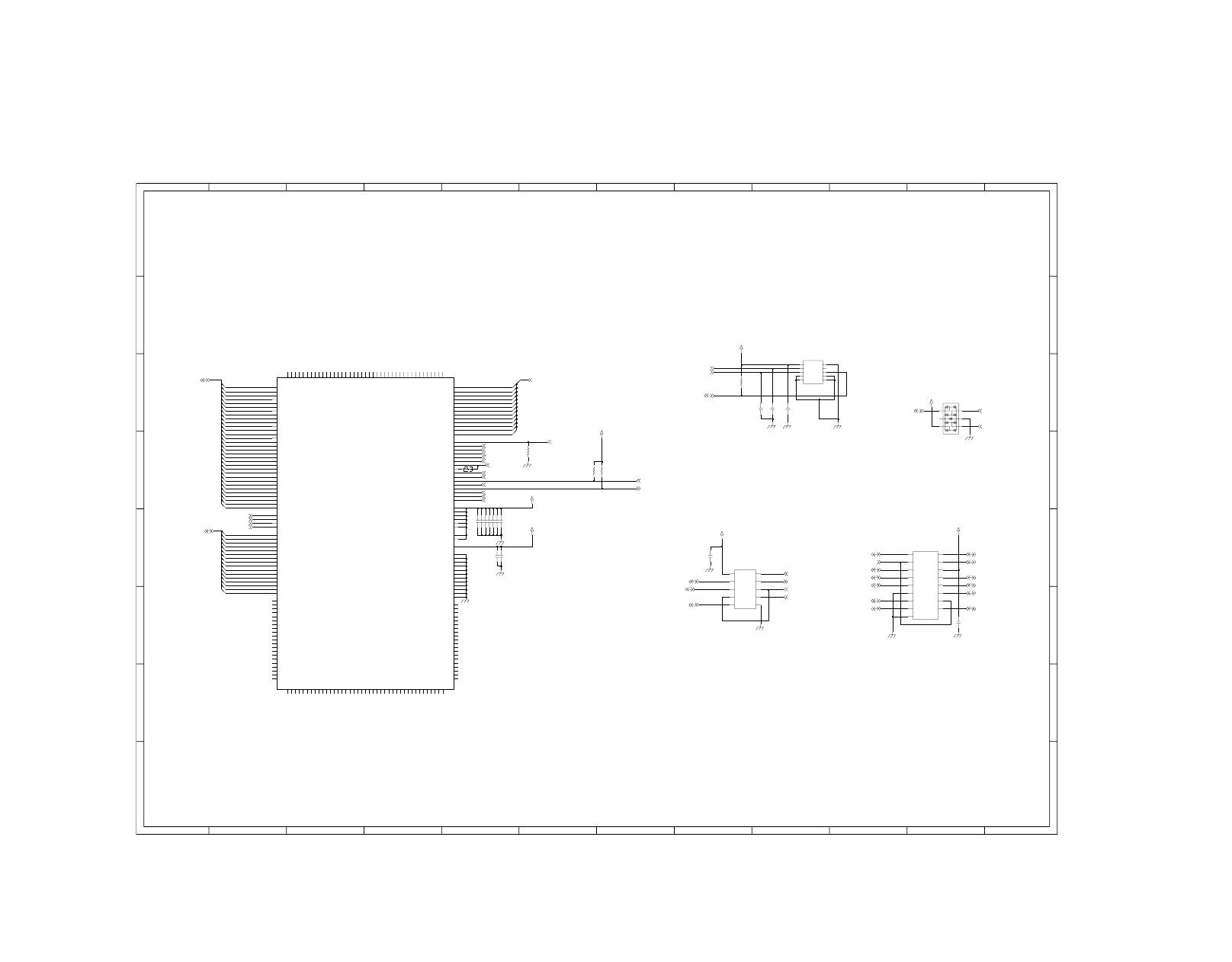
- 174 -
2
12
8
9
B
6
7
H
1
F
11
2
E
F
F
1
E
6
H
A
F
7
11
10
9
5
6
D
9
3
MEMORY (2Gbit 70n NAND FLASH + 1Gbit SDRAM)
D
5
11
3
G
G
G
B
5
D
2
C
3
2
4
1
6
E
G
A
H
12
4
8
12
9
A
B
C
3
MICRO SD SELECT MSM AND MMP
H
E
8
1
4
A
7
USIM
B
8
7
10
10
C
4
11
5
10
D
C
12
C408
0.1u
0.1u
C405
C411
0.1u
_WP
L6
1u
C402
F7
VSS2
G2
VSS3
G13
VSS4
L13
VSS5
P2
VSS6
VSS7
P13
R8
VSS8
VSS9
U2
E6
_CAS
_CE
M9
E5
_CS1
_CS2
D7
D5
_RAS
M10
_RE
D6
_WED
K6
_WEN
NC98
T3
NC99
T7
M2
RY__BY
C7
VCCD1
VCCD2
D2
VCCD3
D13
V3
VCCD4
VCCD5
V8
VCCD6
V12
K12
VCCN2
VCCQD1
V4
V9
VCCQD2
C6
VSS1
VSS10
U6
VSS11
U10
U13
VSS12
NC83
N3
NC84
N4
N5
NC85
N6
NC86
NC87
N9
N10
NC88
N11
NC89
B1
NC9
NC90
N12
N13
NC91
NC92
P7
P8
NC93
NC94
R2
R7
NC95
NC96
R9
T2
NC97
K5
NC69
A13
NC7
NC70
K10
K11
NC71
NC72
K13
K14
NC73
L1
NC74
NC75
L2
NC76
L3
L4
NC77
NC78
L5
L14
NC79
A14
NC8
NC80
M5
M6
NC81
NC82
N2
NC54
H5
H6
NC55
NC56
J2
J3
NC57
J4
NC58
NC59
J5
NC6
A12
NC60
J6
J10
NC61
NC62
J11
J12
NC63
NC64
J13
NC65
K1
K2
NC66
K3
NC67
NC68
K4
A4
NC4
F11
NC40
NC41
F12
F13
NC42
G3
NC43
G4
NC44
G5
NC45
NC46
G6
G7
NC47
NC48
G8
G9
NC49
A11
NC5
NC50
G10
H2
NC51
NC52
H3
H4
NC53
E7
NC25
NC26
E8
E9
NC27
NC28
E10
E11
NC29
NC3
A3
NC30
E12
E13
NC31
NC32
F2
F3
NC33
NC34
F4
F5
NC35
NC36
F6
NC37
F8
F9
NC38
NC39
F10
Y12
NC121
NC122
Y13
Y14
NC123
B11
NC13
B12
NC14
NC15
B13
B14
NC16
NC17
C1
C2
NC18
C5
NC19
A2
NC2
C13
NC20
C14
NC21
D1
NC22
NC23
D14
E1
NC24
NC107
V14
W1
NC108
W2
NC109
B3
NC11
NC110
W3
W4
NC111
NC112
W11
W12
NC113
NC114
W13
W14
NC115
NC116
Y1
Y2
NC117
Y3
NC118
Y4
NC119
B4
NC12
NC120
Y11
L10
IO3
L12
IO4
J9
IO5
H12
IO6
H10
IO7
IO8
G12
IO9
M12
A1
NC1
B2
NC10
T13
NC100
U1
NC101
NC102
U3
U14
NC103
V1
NC104
NC105
V2
NC106
V13
U7
DQ7
DQ8
T9
T10
DQ9
U8
DQM0
DQM1
T8
V7
DQM2
U9
DQM3
M11
IO1
IO10
L9
IO11
L11
IO12
K9
H13
IO13
IO14
H11
IO15
H9
IO16
G11
M13
IO2
P5
DQ20
DQ21
R5
DQ22
P6
R6
DQ23
P9
DQ24
P10
DQ25
DQ26
R10
DQ27
P11
DQ28
R11
P12
DQ29
V5
DQ3
DQ30
R12
R13
DQ31
DQ4
U5
DQ5
T6
V6
DQ6
D8
CKE
M4
CLE
C8
CLK
DQ0
U4
DQ1
T4
DQ10
V10
T11
DQ11
DQ12
U11
V11
DQ13
DQ14
T12
U12
DQ15
DQ16
P3
DQ17
R3
DQ18
P4
R4
DQ19
DQ2
T5
C3
A0
D3
A1
E4
A10
D9
A11
A12
C9
E3
A2
E2
A3
D12
A4
C12
A5
D11
A6
C11
A7
D10
A8
C10
A9
M3
ALE
C4
BA0
D4
BA1
TYA000BC00HOGG
U402
R402
100K
1
NC1
NC2
5
NC3
9
13
NC4
15
NO1
3
NO2
NO3
7
NO4
11
17
PGND
V+
14
U401
MAX4701ETE+T
16
COM1
COM2
4
8
COM3
COM4
12
GND
6
2
IN1_IN2
10
IN3_IN4
33p
C401
10K
R403
0.01u
C412
C406
0.1u
VREG_USIM_3.0V
VREG_MSMP_2.7V
C410
0.01u
C413
0.01u
C400
33p
0.1u
C407
GND3
9
10
GND4
0.1u
C409
J400
1
C1
2
C2
C3
3
4
C5
C6
5
C7
6
GND1
7
8
GND2
0.1u
C404
R401
100K
+VPWR
0
R404
VREG_MSMP_2.7V
VREG_USIM_3.0V
+VPWR
2
NO1
10
NO2
VCC
1
SLAS4717EPMTR2G
U400
COM1
3
COM2
9
GND
6
4
IN1
8
IN2
NC1
5
7
NC2
0.1u
15K
R400
VREG_MSME_1.8V
C403
1
2
3
4
5
6
D400
PLR0504F
MSM_MICROSD_DATA[0]
MMP_MICROSD_DATA[0]
MSM_MICROSD_DATA[1]
MMP_MICROSD_DATA[1]
MSM_MICROSD_DATA[2]
MMP_MICROSD_DATA[2]
MICROSD_DATA[2]
USIM_P_RST_N
USIM_P_DATA
USIM_P_CLK
MSM_MICROSD_CLK
MSM_MICROSD_CMD
NAND_READY
RESOUT_N
MMP_MICROSD_DATA[3]
MSM_MICROSD_DATA[3]
USIM_P_DATA
USIM_P_RST_N
USIM_P_CLK
SDRAM_CLK
SDRAM_WE_N
SDRAM_ADDR[14]
SDRAM_ADDR[13]
SDRAM_CLK_EN
NAND_CLE
NAND_ALE
NAND_CS_N
EBI2_OE_N
EBI2_DATA[8]
EBI2_DATA[9]
EBI2_DATA[10]
EBI2_DATA[11]
EBI2_DATA[12]
EBI2_DATA[13]
EBI2_DATA[14]
EBI2_DATA[15]
MMC_SELECT_N
MMP_MICROSD_CMD
MICROSD_CLK
MICROSD_CMD
MMP_MICROSD_CLK
MMC_SELECT_N
MICROSD_DATA[3]
MICROSD_DATA[1]
MICROSD_DATA[0]
SDRAM_DATA[26]
SDRAM_DATA[27]
SDRAM_DATA[29]
SDRAM_DATA[30]
SDRAM_DATA[31]
SDRAM_DATA[16]
SDRAM_DATA[17]
SDRAM_DATA[22]
SDRAM_DATA[18]
SDRAM_DATA[19]
SDRAM_DATA[23]
SDRAM_DATA[20]
SDRAM_DATA[21]
SDRAM_DATA[0:31]
SDRAM_ADDR[1]
SDRAM_ADDR[2]
SDRAM_ADDR[4]
SDRAM_ADDR[3]
SDRAM_ADDR[9]
SDRAM_ADDR[5]
SDRAM_ADDR[8]
SDRAM_ADDR[7]
SDRAM_ADDR[6]
SDRAM_ADDR[10]
SDRAM_ADDR[11]
SDRAM_ADDR[12]
SDRAM_ADDR[0]
SDRAM_ADDR[0:12]
SDRAM_CS_N
EBI2_WE_N
SDRAM_CAS_N
SDRAM_RAS_N
SDRAM_DQM[0]
SDRAM_DQM[1]
SDRAM_DQM[2]
SDRAM_DQM[3]
EBI2_DATA[0:15]
EBI2_DATA[0]
EBI2_DATA[1]
EBI2_DATA[2]
EBI2_DATA[3]
EBI2_DATA[4]
EBI2_DATA[5]
EBI2_DATA[6]
EBI2_DATA[7]
SDRAM_DATA[1]
SDRAM_DATA[0]
SDRAM_DATA[6]
SDRAM_DATA[2]
SDRAM_DATA[8]
SDRAM_DATA[7]
SDRAM_DATA[3]
SDRAM_DATA[12]
SDRAM_DATA[10]
SDRAM_DATA[9]
SDRAM_DATA[5]
SDRAM_DATA[4]
SDRAM_DATA[13]
SDRAM_DATA[11]
SDRAM_DATA[15]
SDRAM_DATA[14]
SDRAM_DATA[24]
SDRAM_DATA[25]
SDRAM_DATA[28]
7. CIRCUIT DIAGRAM
LGE Internal Use Only
Copyright © 2007 LG Electronics. Inc. All right reserved.
Only for training and service purposes
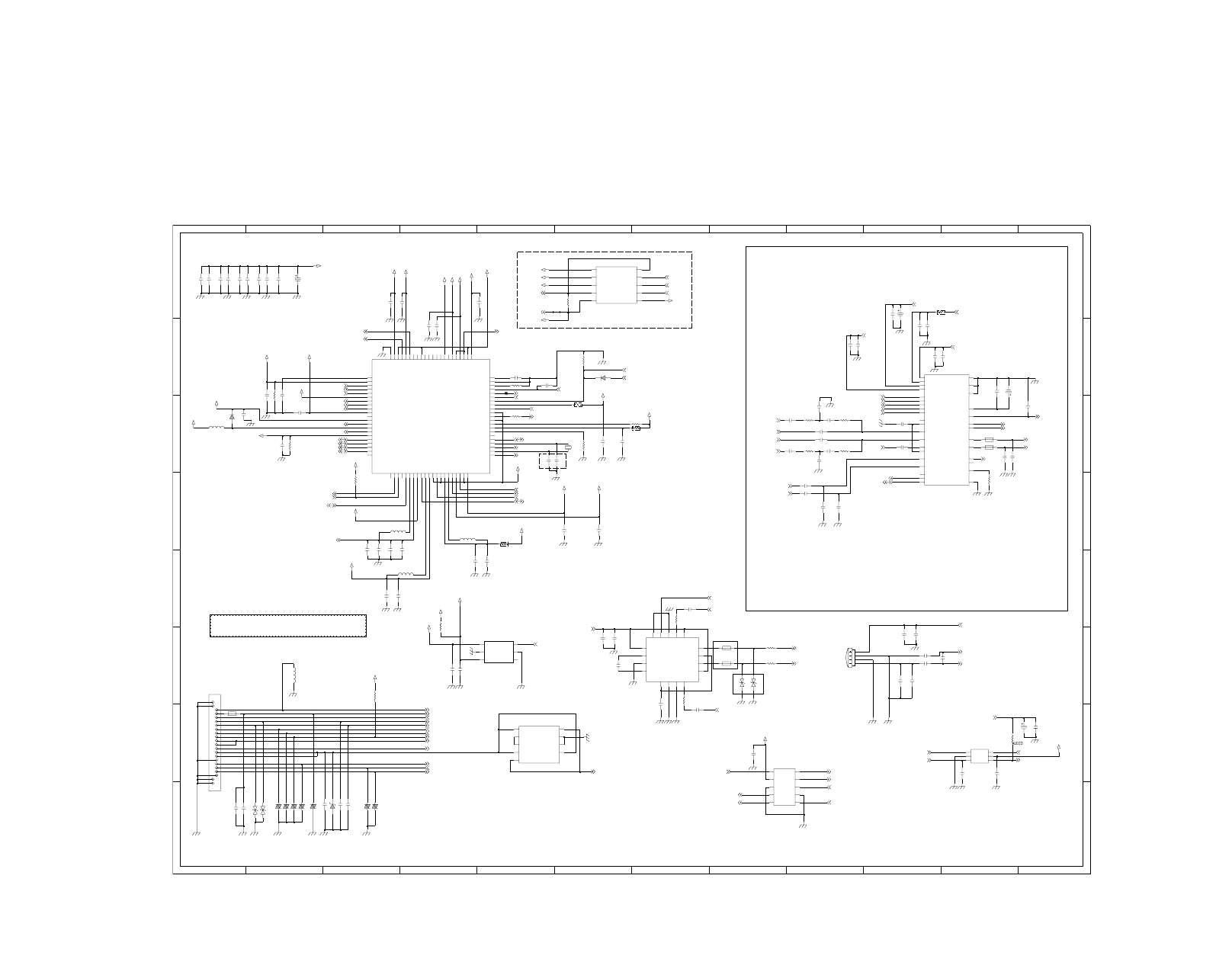
- 175 -
8
C
A
VDD_MAIN : 0.1uF
10
9
4
8
H
B
1
USB/REMOCON_SEL
PMIC
10
CHARGING
VSW_5V : 4.7uF
6
1608
F
4
H
7
A
VDD_RUIM : 0.1uF
MMI 18Pin CONNECTOR
E
1608
VDD_MSMC : 4.7uF
Rev. 1.0
12
9
1608
11
1608
VDD_WLAN : 0.1uF
A
VDD_ANA : 0.1uF
--->> USB_VBUS , FLASH_DRV_N , KPD_DRV_N , KEY_ON_SW_N , MOT_PWR-
OVP
D
10
10
7
F
E
G
D
4
1608
H
6
5
1
Rev. 1.1
7
11
2012
11
3
G
12
3
G
1608
HEADPHONE AMP
E
2
VDD_MSM : 0.1uF
3
5
1608
8
2
7
A
8
3
F
C
VDD_MSME : 4.7uF
PMIC VPWR BYPASS
2
1
4
G
AUDIO DAC/ADC, AMP etc. (WM8983)
PQ
PQ
11
E
1
(1%)
9
H
F
B
CAM/HP MIC SEL
1608
12
12
VDD_PA : 4.7uF
2
Power Line --> Route carefully!!!!!
MIC
9
Draw the Artwork_line thickly !!!!!
U505
NUS3065MUTAG
CNTRL
3
4
DRAIN
DRAIN_THERMAL
9
GATE
6
2
GND
IN
1
7
OUT
5
SRC
8
VCC
2.2u
C511
R524
68
EVLC14S02050
C504
+VPWR
VA505
SVSS
16
_SHDN
4.7u
C1N
4
2
C1P
INL+
15
INL_
14
7
INR+
INR_
8
OUTL
12
OUTR
10
3
PGND
PVDD
1
5
PVSS
P_G
17
SGND
6
13
SVDD1
9
SVDD2
11
U504
MAX9722BETE
R520
0
VREG_MSMP_2.7V
0.1
R504
FB501
4.7u
C565
R505
VREG_MSMC_1.2V
470K
10u
FB500
C555
C577
1u
RB521S-30
D501
80
REF_OUT(MPP8)
VREG_SYNT
81
AMUX_OUT
82
VDD_MAIN
83
VREG_TCXO
84
GND_SLUG
85
PON_RESET_N
9
VREG_RFTX
73
74
SPKR_BYP
75
SPKR_OUT_P
SPKR_IN_P
76
VDD_SPKR
77
SPKR_IN_M
78
SPKR_OUT_M
79
FLSH_DRV_N
8
CBL1PWR_N(MPP4)
66
VREG_RFRX2
67
CBL0PWR_N(MPP3)
68
69
VREG_RFRX1
BAT_FET_N
7
AMUX_IN1(MPP1)
70
VDD_RF
71
AMUX_IN2(MPP2)
72
MSM_INT_N
59
VBAT
6
VCOIN
60
61
REF_ISET
REF_GND
62
REF_BYP
63
VREG_WLAN
64
VDD_WLAN
65
SBST
51
VDD_MSM
52
TCXO_OUT
53
54
VDD_ANA
TCXO_EN
55
VREG_MSMA
56
PS_HOLD
57
TCXO_IN
58
XTAL_IN
44
SLEEP_CLK
45
46
XTAL_OUT
SBDT
47
VBACKUP
48
SBCK
49
ISNS_M
5
VREG_MSMP
50
VSW_MSME
37
RUIM_CLK(MPP10)
38
39
VREG_MMC
CHG_CTL_N
4
RUIM_M_RST(MPP5)
40
VDD_RUIM
41
VREG_RUIM
42
RUIM_RST(MPP6)
43
ISNS_P
3
RUIM_M_IO(MPP11)
30
31
VSW_MSMC
VREG_MSMC
32
VDD_MSMC
33
RUIM_M_CLK(MPP9)
34
VDD_MSME
35
VREG_MSME
36
LCD_DRV_N
22
KPD_DRV_N
23
24
KPDPWR_N
VIB_DRV_N
25
RUIM_IO(MPP12)
26
VSW_PA
27
VREG_PA
28
VDD_PA
29
USB_CTL_N
15
USB_VBUS
16
USB_DAT
17
USB_D_P
18
19
USB_SE0
VCHG
2
USB_D_M
20
GP1_DRV_N(MPP7)
21
ADC_BYP
1
VREG_USB
10
11
USB_ID
VREG_5V
12
USB_OE_N
13
VSW_5V
14
NC7SB3157L6X
A
4
B0
3
1
B1
2
GND
6
S
5
VCC
U501
PM6650-2M
SD12T1G
D
502
U506
VBATT
10u
C563
NA
+VPWR
C550
121K
C580
47p
R506
1u
C529
4.7uH
L503
0.1u
C514
C509
4.7u
+VPWR
VREG_MSMA_2.6V
R525
68
1000p
C557
C535
EVLC14S02050
VA504
1u
600
FB503
C532
1u
0.1u
C502
VGA_VDD_1.8V
R2_GPIO3
6
RIN
5
4
RIP
ROUT1
29
ROUT2
23
16
SCLK
SDIN
17
27
VMID
+VPWR
DACDAT
10
DBVDD
14
DCVDD
13
12
DGND
L2_GPIO2
3
LIN
2
1
LIP
LOUT1
30
25
LOUT2
7
LRC
11
MCLK
MICBIAS
32
18
MODE
OUT3
22
21
OUT4
33
PGND
U502
ADCDAT
9
28
AGND1
24
AGND2
AUXL
19
AUXR
20
31
AVDD1
AVDD2
26
8
BCLK
15
CSB_GPIO1
4.7u
C520
WM8983
C568
22n
0.1u
FB502
600
C559
4.7u
C561
0.1u
C540
33u
C500
C533
4.7n
R511
18K
0.22u
10K
R507
C578
BASE1
8
BASE2
7
3
COLLECTOR
DRAIN
5
1
EMITTER1
EMITTER2
2
6
GATE
9
P_COLLECTOR
P_DRAIN
10
SOURCE
4
X500
32.768KHz
12
NUS3116MTR2G
U500
R509
VREG_TCXO_2.85V
51
C587
4
7p
2.2u
C515
R533
0
R522
15K
4.7u
C508
VA508
PRSB6.8C
VA501
ULCE0505C015FR
10u
C579
10u
C525
C503
0.1u
10p
C588
VREG_MSMP_2.7V
1u
C572
VREG_5V
C571
1u
4.7u
C538
SEL
10
9
VCC
8
_OE
C506
4.7u
FSUSB30UMX U507
D+
3
D-
5
GND
4
1
HSD1+
7
HSD1-
2
HSD2+
HSD2-
6
15K
R529
C584
VBATT
0.1u
C534
EVLC14S02050
1u
VA503
MIDI_3.3V
0.01u
C581
C528
C507
4.7u
VREG_BT_2.85V
0.1u
10u
C513
1u
C570
VREG_USB_3.3V
4.7u
C558
R515
51K
1u
C512
C569
NA
VREG_SYNTH_2.6V
C510
1u
C537
4.7u
L500
100K
R519
smd_2520h1_6_r
4.7uH
4.7n
C542
C560
NA
C531
4.7u
C564
47p
0.1u
C505
1K
R516
0.1u
C501
C556
VA500
ULCE0505C015FR
47K
R514
0.1u
8
9
12
13
14
15
16
17
18
19
2
20
21
22
3
4
5
6
7
CN500
1
10
11
R510
1K
C541
1u
+5V_PWR
1u
C549
1u
C548
10K
R518
C536
1u
4.7uH
L502
TP500
C553
C518
4.7u
2.2u
R528
100K
PRSB6.8C
C574
VA502
EVLC14S02050
+VPWR
C590
2.2u
VREG_WM_2.7V
C539
1u
2
G1
3
G2
1
O
4
P
0
R508
SPM0204HE5-PB-3
MIC500
D500
RB521S-30
22p
C546
12n
C547
33p
C575
C524
0.1u
+VPWR
10p
C522
0.1u
ind_2x1_6h1_r
C583
4.7uH
L501
0.1u
C527
USB_VBUS
+VPWR
NA
C544
10p
C576
EVLC14S02050
C519
VA506
C573
VBATT
+5V_PWR
VBATT
0.1u
C552
PRSB6.8C
USB_VBUS
VREG_USIM_3.0V
2.2u
C551
NA
VREG_MSME_1.8V
C521
0.1u
C567
22n
+VPWR
VA507
PRSB6.8C
R1180D331B
CE_OR_NC
6
2
GND1
5
GND2
NC
4
VDD
1
VOUT
3
47p
U503
C586
22p
C545
C543
NA
R513
FB504
0
51K
R512
2.2K
R530
C589
VREG_MSMP_2.7V
12n
33p
C530
C585
1u
18K
R517
2.2uH
L504
R521
NA
1u
C523
MMP_VDD_USB_3.3V
1u
C566
VREG_MMC_3.0V
C562
VREG_5V
0.22u
22u
C554
1u
C526
C516
4.7u
C517
0.1u
MIDI_EAR_R
MIC_PWR
MID_MICP
WM_EN
MIC_PWR
TV_OUT
ICHARGE
EAR_MIC_P
RMT_PWR_ON_N
MMP_A_MCLK
EAR_SENSE_N
CAM_MIC+
EAR_MIC_P
CODEC_I2C_SCL
CODEC_I2C_SDA
MICBIAS
HP_R
HP_L
MIDI_EAR_L
HP_EAR_L
MIC2P
HP_EAR_R
MID_MICP
SPK_L
SPK_R
FM_AUDIO_L
FM_AUDIO_R
MMP_A_BCLK
MMP_ADO_DACDAT
MMP_A_LRCLK
MMP_ADI_ADCDAT
SPK_OUT-
SPK_OUT+
VREG_5V
VREG_WM_2.7V
VREG_MSME_1.8V
MIDI_3.3V
RMT_INT-USB_D+
RMT_ADC-USB_D-
VBATT
+5V_PWR
RMT_INT
RMT_ADC
EAR_SENSE_N
USB_D+
USB_D-
RMT_INT-USB_D+
RMT_ADC-USB_D-
FM_ANT
UART_TXD
MIDI_3.3V
HP_AMP_EN
HP_EAR_L
HP_EAR_R
GSM_PA_PWR_CTL_REF
AMUX_OUT
RESET_IN_N
BUFF_TCXO
PS_HOLD
FLSH_DRV_N
ICHARGEOUT
CHG_CNT_N
USB_CNT_N
BATT_FET_N
MIC1P
MIC1N
VREG_RF_SMPS
USB_VBUS
UART_RXD
MIDI_EAR_L
MIDI_EAR_R
EAR_SENSE_N
USB_OE_N
USB_CNT_N
USB_DAT
MSM_USB_D+
USB_SE0
MSM_USB_D-
KYPD_LED_EN
PM_ON_SW_N
USIM_P_DATA
ICHARGE
USIM_DATA
USIM_CLK
USIM_P_CLK
CHG_CNT_N
USIM_RST_N
USIM_P_RST_N
SLEEP_CLK
SSBDT_PM
ICHARGEOUT
TCXO_EN
JTAG_PS_HOLD
TCXO_PM
PM_INT_N
V_BACK_UP
RMT_PWR_ON_N
BATT_FET_N
7. CIRCUIT DIAGRAM
LGE Internal Use Only
Copyright © 2007 LG Electronics. Inc. All right reserved.
Only for training and service purposes
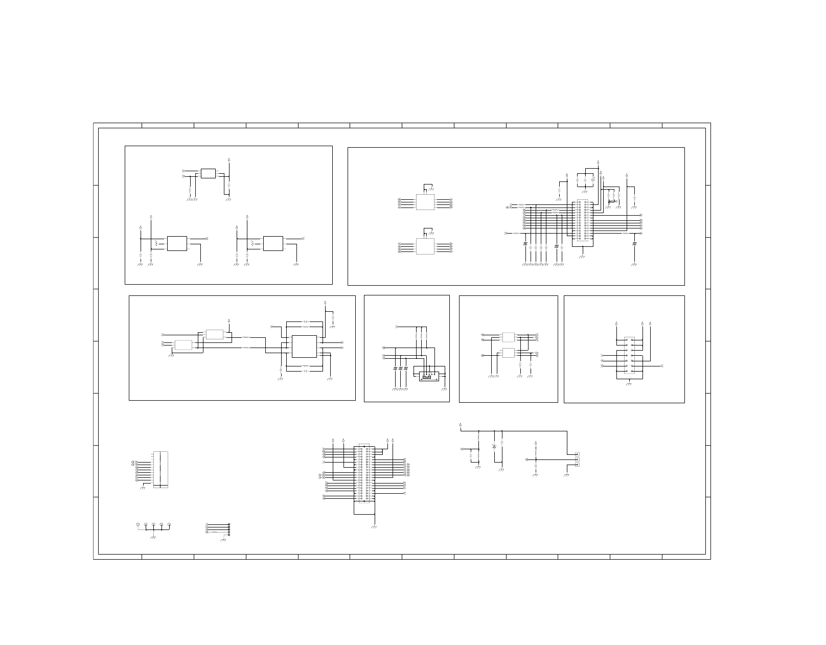
- 176 -
PWR
URXD
UTXD
3G
2.5G
GND
RX
TX
VCHAR
ON_SW
VBAT
C
H
F
D
H
AXK714247G
1
5
2
G
E
2
B
12
C
E
6
F
A
GB042-30S-H10-E3000
H
2
9
3
1
4
5
4
10
E
G
C
D
7
150mA
10
ESSY0004701
1
11
11
11
7
MODE SWITCH
3
9
10
B
H
5
8
D
5MP CAM LDO
6
7
Strobe(Xenon Lamp) Flash Interface
10
12
4
8
JTAG CONNECTOR
FOR NEST JIG
5
D
MODE1
PCB ARRAY TP
2
(BATTERY PAD 1.5 X 3.4)
G
12
8
3
F
C
MAIN - SUB B to B Conn.
8
A
9
6
F
9
4
3
5M CAMERA INTERFACE
6
12
MODE3
11
E
7
1608
1
SWITCH FOR 5M VT CALL
MODE2
VGA CAM LDO
150mA
G
AXK740327G
LINEAR MOTOR DRIVER ( AUDIO AMP )
1u
C603
1u
CAM_VDD_SA_2.7V
VREG_MMC_3.0V
CAM_VDD_IO_2.7V
P2 P3
P4
C608
SSP-132MHT
SW600
G1
G2
G3
G4
P1
R613
51K
C605
VBATT
0.1u
C615
1u
OUT611
1u
C619
EVLC14S02050
VA604
10p
C610
30
17
18
19
20
21
22
23
24
14
15
2
3
4
5
6
7
8
9
16
25
26
27
28
29
CN600
1
10
11
12
13
TP602
VREG_MSMP_2.7V
0.1u
U603
TC7SZ86FU
GND
3
2
IN_A
1
IN_B
4
OUT_Y
VCC
5
C623
OJ603
U604
NC7SB3157L6X
A
4
B0
3
1
B1
2
GND
6
S
5
VCC
0.1u
C612
C606
10p
R601 10
0.1u
C626
R615
100K
0.1u
C622
U600
BH28PB1WHFV
BGND
6
GND
2
SEL
5
1
STBY
VIN
3
4
VOUT
C620
8
9
2200p
3
30
31
32
33
34
35
36
37
38
39
4
40
5
6
7
15
16
17
18
19
2
20
21
22
23
24
25
26
27
28
29
CN603
G1
G2
1
10
11
12
13
14
OJ602
CAM_VDD_SA_2.7V
0
R626
1u
C617
R607
33
TP600
1u
C604
VA603
EVLC14S02050
5
G1
10
G2
1
INOUT_A1
INOUT_A2
2
3
INOUT_A3
INOUT_A4
4
9
INOUT_B1
8
INOUT_B2
INOUT_B3
7
6
INOUT_B4
ICVE10184E070R100FR
FL600
U602
R1114D271D
CE_OR_NC
6
2
GND1
5
GND2
NC
4
VDD
1
VOUT
3
NC7SB3157L6X
U607
4
A
3
B0
B1
1
GND
2
S
6
VCC
5
0.1u
C621
VGA_VDD_2.7V
TP604
OUT608
OJ604
100K
R611
INSTPAR
0.1u
D600
PSD05-LF
+VPWR
C607
10p
C611
TP603
GND1
2
GND2
5
4
NC
1
VDD
3
VOUT
VREG_MSMP_2.7V
+VPWR
CAM_VDD_AF_2.7V
R1114D271D
U601
6
CE_OR_NC
CAM_VDD_CORE_1.2V
OJ601
0.1u
C627
51K
R612
+VPWR
100K
R619
470K
R621
VA601
ICVL0518100Y500FR
1u
7
8
9
10
11
12
13
14
C616
CN601
1
2
3
4
5
6
2200p
VA602
TP601
C624
C614
EVLC18S02015
0.1u
C601
CTS
12
DSR
10
1
GND
NC1
4
7
NC2
NC3
8
9
NC4
5
ON_SW
11
RTS
RX
2
3
TX
VBAT
6
0.1u
C625
+VPWR
CN602
10u
C618
+VPWR
ICVL0518100Y500FR
VA600
10u
1u
C600
R610
100K
VREG_BT_2.85V
VA605
EVLC14S02050
CAM_VDD_IO_2.7V
VREG_5V
80.6K
OJ600
R622
R604
10
VREG_MSMP_2.7V
OUT614
CAM_VDD_SD_1.8V
10
R603
10p
VREG_MMC_3.0V
+VPWR
C613
C609
0.1u
R608
10
G1
5
G2
10
INOUT_A1
1
2
INOUT_A2
INOUT_A3
3
INOUT_A4
4
9
INOUT_B1
INOUT_B2
8
7
INOUT_B3
INOUT_B4
6
GND
3
2
IN_A
1
IN_B
4
OUT_Y
VCC
5
FL601
ICVE10184E070R100FR
VREG_MMC_3.0V
U605
TC7SZ86FU
5
VO+
8
VO-
_SHUTDOWN
1
680K
R623
U606
TPA6205A1DRBR
2
BYPASS
7
GND
IN+
3
4
IN-
9
PGND
VDD
6
C602
1u
R602 10
VGA_CAM_PWR_EN
+5V_PWR
R614
51K
MMP_CAM_DATA[3]
5M_CAM_DATA[0]
5M_CAM_DATA[1]
5M_CAM_DATA[2]
5M_CAM_DATA[3]
MMP_CAM_DATA[4]
MMP_CAM_DATA[5]
MMP_CAM_DATA[6]
MMP_CAM_DATA[7]
5M_CAM_DATA[4]
5M_CAM_DATA[5]
5M_CAM_DATA[6]
5M_CAM_DATA[7]
VBATT
UART_TXD
UART_RXD
PM_ON_SW_N
MSM_USB_D+
MSM_USB_D-
USB_VBUS
MMP_CAM_PWR_EN
SPK_OUT+
SPK_OUT-
VBATT
HOOK_SENSE_N
EAR_MIC_P
5M_CAM_MCLK
CAM_MCLK
VGA_CAM_MCLK
STROBE_TRIGGER
PM_ON_SW_N
UART_RXD
UART_TXD
MMP_CAM_PCLK
5M_CAM_DATA[0]
5M_CAM_DATA[1]
5M_CAM_DATA[2]
5M_CAM_DATA[3]
5M_CAM_DATA[4]
5M_CAM_DATA[5]
5M_CAM_DATA[6]
5M_CAM_DATA[7]
MMP_CAM_RESET_N
MMP_CAM_INT
MMP_CAM_HSYNC
MMP_CAM_VSYNC
MMP_I2C_SDA
MMP_I2C_SCL
5M_CAM_MCLK
VREG_MSMP_2.7V
CAM_MODE3_N
CAM_MODE2_N
CAM_MODE1_N
MMP_CAM_DATA[0]
MMP_CAM_DATA[1]
MMP_CAM_DATA[2]
MICROSD_DATA[1]
MICROSD_DETECT
MICROSD_CLK
MICROSD_DATA[0]
MICROSD_CMD
CAM_VDD_AF_2.7V
CAM_MIC+
WHEEL_SW_L
WHEEL_SW_R
CAM_VDD_SD_1.8V
V_BACK_UP
MMP_CAM_MCLK
5M_CAM_MCLK
STROBE_TRIGGER
FLSH_DRV_N
VBAT_SENSE
VBAT_TEMP
CAM_SELECT_N
LIN_PWM_MAG
LIN_INVERTER
LIN_PWM_FREQ
LIN_MOTOR_EN
MOTOR-
MOTOR+
TCXO_BT
BT_TX_RX_N
BT_SBST
BT_SBCK
BT_SBDT
BT_CLK
BT_DATA
MMP_STROBE_CHARGE
MMP_STROBE_READY
MMP_CAM_PWR_EN
MMP_CAM_PWR_EN
+VPWR
MICROSD_DATA[3]
MICROSD_DATA[2]
7. CIRCUIT DIAGRAM
LGE Internal Use Only
Copyright © 2007 LG Electronics. Inc. All right reserved.
Only for training and service purposes
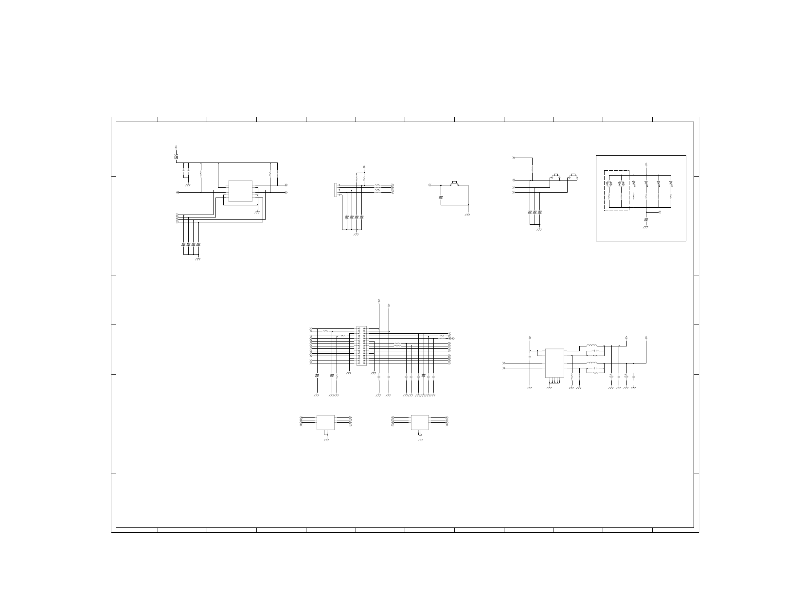
- 177 -
2
12
D
9
6
KEY PCB BACKLIGHT LEDs
G
D
2
4
5
C
12
2
TOUCH SCREEN DRIVER IC
F
8
4
E
12
11
KEY
A
10
F
10
H
F
C
H
7
3
11
END
E
G
E
G
12
SIDE KEY
F
C
1
5
D
7
A
9
8
CLR
H
6
E
10
3
9
2
3
3
B
1
4
ON_SW KEY
11
(GREEN)
Rev. 1.1
(WHITE)
(RED)
PQ
6
10
5
8
D
Touch Driver IC change : TSC2003 -> TSC2007
4
9
8
B
1
H
5
7
G
11
SEND
6
7
C
1
R711
47
470
R709
R710
470
470
R708
LD701
SSC-FR104-II1
0
R700
10
R719
51K
R706
4.7uH
L700
R701
CAM_VDD_CORE_1.2V
VA712
EVLC14S02050
VGA_VDD_2.7V
51K
R712
6
200
5
G1
10
G2
INOUT_A1
1
2
INOUT_A2
INOUT_A3
3
4
INOUT_A4
9
INOUT_B1
INOUT_B2
8
7
INOUT_B3
INOUT_B4
100p
ICVE10184E070R100FR
FL701
701
C704
EVLC14S02050
VA709
R725
10
VA704
EVLC14S02050
C702
100p
10
R724
EVLC14S02050
VA711
700
A0
A1
C2
A1
AUX
GND
D2
PENIRQ-
B1
D1
SCL
C1
SDA
VDD_REF
A2
A3
X+
C3
X-
B3
Y+
D3
Y-
VA702
TSC2007IYZGR
U700
B2
EVLC14S02050
2.2u
C706
51K
R705
0.1u
LCD_VDD_2.8V
C701
16
25
26
27
28
29
30
17
18
19
20
21
22
23
24
1
10
11
12
13
14
15
2
3
4
5
6
7
8
9
CN701
SSC-FR104-II1
200
R714
LD703
VREG_MSMP_2.7V
R731
56K
R707
470
L701
4.7uH
C711
0.1u
R703
2.7K
10p
C713
EVL14K02200
VA708
EVL14K02200
VA700
R718
10
56K
R730
4.7u
C705
EVLC18S02015
VA701
EVLC14S02050
VA715
R728
56K
SSC-TWH104-HL
LD704
R715
47
R729
+VPWR
NA
resistor
10p
C715
EVLC14S02050
VA707
EVLC14S02050
VA706
10
R717
VA714
ICVL0518100Y500FR
SSC-TWH104-HL
R713
47
LD700
4.7u
NA
R702
C703
LEGG-S14G
LD702
VA705
10
R720
EVLC14S02050
G1
5
G2
10
INOUT_A1
1
2
INOUT_A2
INOUT_A3
3
4
INOUT_A4
9
INOUT_B1
INOUT_B2
8
7
INOUT_B3
INOUT_B4
6
END
C712
FL700
ICVE10184E070R100FR
5
10p
CN700
1
2
3
4
C700
1u
EVLC18S02015
VA713
C709
0.1u
2.7K
R704
C708
2.2u
MMP_VDD_CORE_1.0V
LD705
LEGG-S14G
VA710
EVLC14S02050
47
R716
VGA_VDD_1.8V
39K
R726
C714
10p
0.1u
C710
FB2
5
GND1
3
6
GND2
LX1
11
8
LX2
PGND1
7
10
PGND2
12
VIN1
9
VIN2
AAT2510IWP-AA-T1
U701
13
BGND
EN1
1
4
EN2
2
FB1
4.7u
C707
X-
KEY_ROW[0]
KEY_ROW[1]
KEY_COL[1]
KEY_COL[0]
KYPD_LED_EN
+VPWR
EVLC14S02050
VA703
VGA_CAM_DATA[2]
VGA_CAM_DATA[3]
VGA_CAM_DATA[4]
VGA_CAM_DATA[7]
I2C_SDA
I2C_SCL
MMP_CAM_VSYNC
MMP_CAM_HSYNC
VGA_CAM_RESET_N
RCV+
RCV-
MOTOR+
MOTOR-
x+
x-
Y+
Y-
MMP_CAM_PWR_EN
MMP_PWR_EN
VGA_CAM_DATA[6]
Y-
Y+
X+
KEY_ROW[2]
PM_ON_SW_N
VREG_MSMP_2.7V
KEY_COL[0]
KEY_COL[1]
TOUCH_PENIRQ_N
TOUCH_I2C_SCL
TOUCH_I2C_SDA
MMP_CAM_DATA[0]
MMP_CAM_DATA[1]
MMP_CAM_DATA[2]
MMP_CAM_DATA[3]
VGA_CAM_DATA[0]
VGA_CAM_DATA[1]
VGA_CAM_DATA[2]
VGA_CAM_DATA[3]
MMP_CAM_DATA[4]
MMP_CAM_DATA[5]
MMP_CAM_DATA[6]
MMP_CAM_DATA[7]
VGA_CAM_DATA[4]
VGA_CAM_DATA[5]
VGA_CAM_DATA[6]
VGA_CAM_DATA[7]
VGA_CAM_PWDN
VGA_CAM_DATA[5]
VGA_CAM_MCLK
MMP_CAM_PCLK
VGA_CAM_DATA[0]
VGA_CAM_DATA[1]
7. CIRCUIT DIAGRAM
LGE Internal Use Only
Copyright © 2007 LG Electronics. Inc. All right reserved.
Only for training and service purposes
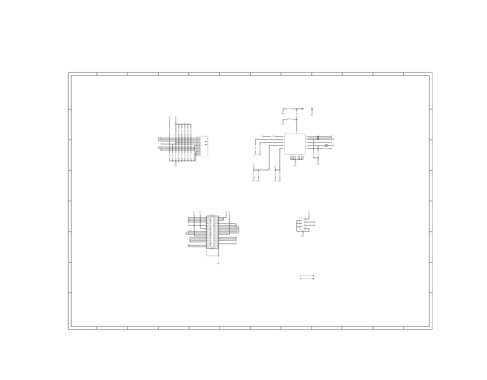
- 178 -
E
B
8
F
5
9
11
6
7
F
A
2
6
8
10
F
11
7
MAIN - SUB B to B Conn.
12
BLUETOOTH
LG INNOTEK
B
D
C
A
C
9
Micro SD
SPEAKER +/-
G
D
5
10
8
WHEEL CONNECTOR
10
11
4
A
E
2
6
F
12
6
C
12
D
7
H
Header
B
B
AXK840225WG
10
D
5
G
9
E
3
11
SPEAKER PAD
5
4
7
3
H
1
8
1
12
A
C
E
9
VREG_MMC_3.0V
C810
33p
TP802
VREG_MSMP_2.7V
TP801
10K
R809
R801
100K
VREG_MSMP_2.7V
100K
R804
C804
1u
35
36
37
38
39
4
40
5
6
7
8
9
20
21
22
23
24
25
26
27
28
29
3
30
31
32
33
34
G1
G2
1
10
11
12
13
14
15
16
17
18
19
2
C802
CN801
1000p
CN800
1
2
3
4
5
6
7
OUT801
0
R807
C803
VREG_MSMP_2.7V
VREG_BT_2.85V
1u
C800
NA
0
R800
BT_ANT
VREG_MMC_3.0V
C814
2.2u
C807
C811
100p
1u
R803
100K
100K
R802
33p
R810
C812
0.1u
GND3
GND4
15
17
PGND1
PGND2
18
19
PGND3
PGND4
20
RX_BB_TX_BB
13
SBCK
11
12
SBDT
SBST
4
5
SYNC_DET_TX_EN
3
VCC_OUT
14
VDD_BAT
VDD_INT
2
VDD_MSM
10
7
XTAL_IN
M800
LBRQ-2B43A
ANT
16
9
CLK_REF
1
GND1
GND2
6
8
33p
C806
C805
C808
33p
33p
+VPWR
BT_GND
VDD
VSS
100K
R805
CD_DAT3_CS
CLK_SCLK
CMD_DI
COMMON
DAT0_DO
DAT1_RSV
DAT2_RSV
DETECT
DUMMY1
DUMMY2
100p
C813
S800 SCHA1B0102
C801
NA
L800
1000p
R806
100K
33p
R811
VREG_BT_2.85V
C809
33p
OUT800
VREG_MSMP_2.7V
TP800
10K
R808
BT_SBDT
BT_SBCK
BT_SBST
BT_TX_RX_N
TCXO_BT
MMP_CAM_PWR_EN
WHEEL_SW_L
WHEEL_SW_R
CAM_MIC+
MICROSD_DATA[3]
MICROSD_DATA[2]
MICROSD_DATA[1]
MICROSD_DATA[0]
MICROSD_CMD
MICROSD_DETECT
MICROSD_CLK
SPK_OUT+
SPK_OUT-
HOOK_SENSE_N
EAR_MIC_P
BT_DATA
BT_CLK
MICROSD_DETECT
MICROSD_CLK
MICROSD_CMD
V_BACK_UP
CAM_VDD_SD_1.8V
CAM_VDD_AF_2.7V
BT_DATA
BT_CLK
WHEEL_SW_L
WHEEL_SW_R
SPK_OUT+
SPK_OUT-
MICROSD_DATA[2]
MICROSD_DATA[1]
MICROSD_DATA[0]
MICROSD_DATA[3]
BT_SBCK
BT_SBDT
BT_SBST
BT_TX_RX_N
TCXO_BT
7. CIRCUIT DIAGRAM
LGE Internal Use Only
Copyright © 2007 LG Electronics. Inc. All right reserved.
Only for training and service purposes
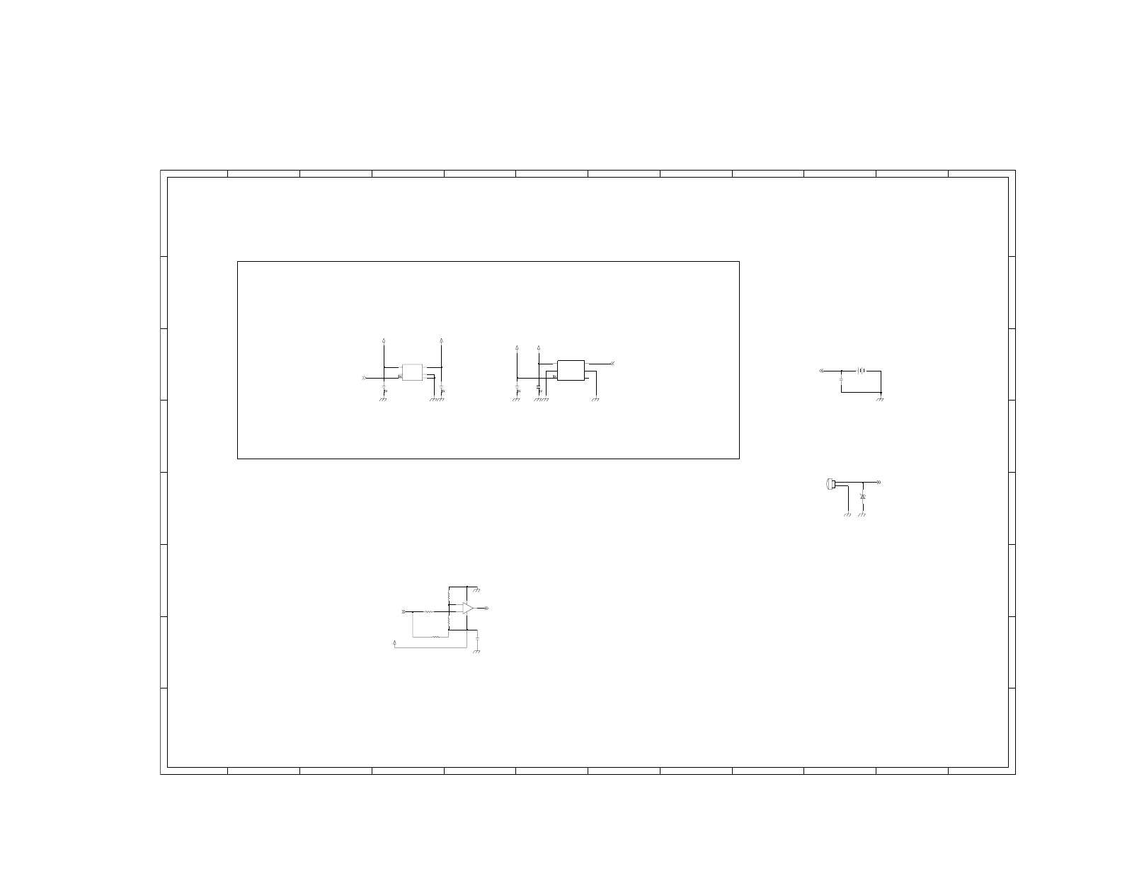
- 179 -
LGE Internal Use Only
D
H
7
6
G
11
F
5
2
G
12
E
10
1
B
5
4
2
150mA
D
6
B
E
A
7
F
A
11
150mA
6
3
6
4
2
F
B
8
H
D
1
8
4
9
7
G
H
12
D
9
B
3
H
10
C
A
11
1
3
7
1
C
12
8
10
5MP CAMERA POWER
10
Headset Hook Switch
F
4
C
C
A
8
CAM MIC
9
3
2
5
E
12
E
11
G
5
BACK_UP BATTERY
9
(VDD_SD)
1u
BAT900
C900
R1114D271D
U901
6
CE_OR_NC
GND1
2
GND2
5
4
NC
1
VDD
3
VOUT
1u
1u
C904
CAM_VDD_SD_1.8V
C903
C901
1u
R905
10K
+VPWR
VREG_MSMP_2.7V
R907
5.1K
C905
0.1u
100K
R906
1M
R904
2
GND
1
OUT
VCC
5
3
VIN+
VIN-
4
1u
U902
NCS2200SQ2T2G
6
CE
GND1
2
GND2
5
NC
4
1
VDD
VOUT
3
C902
CAM_VDD_AF_2.7V
U900
R1114D181D
INSTPAR
PLW0501H-LF
ZD900
MIC900
SPOB-413S42-RC3310BC
1
2
+VPWR
V_BACK_UP
CAM_MIC+
MMP_CAM_PWR_EN
MMP_CAM_PWR_EN
HOOK_SENSE_N
EAR_MIC_P
7. CIRCUIT DIAGRAM
Copyright © 2007 LG Electronics. Inc. All right reserved.
Only for training and service purposes
- 180 -
LGMC
8
9
11
1
2
D
F
G
A
12
D
A
4
6
B
11
12
1
2
H
G
D
11
2
10
11
7
5
6
12
C
A
7
F
3
12
CONNECT TO CAMERA MODULE
C
AXT628124-Header
B
3
2
E
10
D
E
8
G
1
F
10
4
5
8
H
5
B
5
4
C
8
9
6
B
7
10
H
A
9
3
4
C
1
3
6
7
H
GB042-30P-H1--E3000
ENBY0041601
CONNECT TO MAIN PCB
E
F
CAMERA FPCB CONNECTOR
G
9
E
30
31
32
4
5
6
7
8
9
17
18
19
2
20
21
22
23
24
25
26
27
28
29
3
CN1001
1
10
11
12
13
14
15
16
CAM_VDD_SA_2.7V CAM_VDD_AF_2.7V
CAM_VDD_SD_1.8V
CAM_VDD_IO_2.7V
CAM_VDD_IO_2.7V
CAM_VDD_SA_2.7V
TP1003
CAM_VDD_CORE_1.2V
CAM_VDD_AF_2.7V
TP1002
20
21
22
23
24
TP1000
TP1001
4
5
6
7
8
9
16
25
26
27
28
29
30
17
18
19
1
10
11
12
13
14
15
2
3
CAM_VDD_SD_1.8V
CAM_VDD_CORE_1.2V
CN1000
STROBE_TRIGGER
MMP_CAM_PCLK
MMP_CAM_INT
5M_CAM_DATA[7]
5M_CAM_DATA[5]
5M_CAM_DATA[3]
5M_CAM_DATA[1]
MMP_CAM_RESET_N
MMP_CAM_HSYNC
MMP_CAM_VSYNC
MMP_I2C_SDA
MMP_I2C_SCL
MMP_CAM_MCLK
5M_CAM_DATA[0]
5M_CAM_DATA[2]
5M_CAM_DATA[4]
5M_CAM_DATA[6]
STROBE_TRIGGER
MMP_CAM_PCLK
MMP_CAM_INT
5M_CAM_DATA[7]
5M_CAM_DATA[5]
5M_CAM_DATA[3]
5M_CAM_DATA[1]
MMP_CAM_MCLK
MMP_I2C_SCL
MMP_I2C_SDA
MMP_CAM_VSYNC
MMP_CAM_HSYNC
MMP_CAM_RESET_N
5M_CAM_DATA[6]
5M_CAM_DATA[4]
5M_CAM_DATA[2]
5M_CAM_DATA[0]
7. CIRCUIT DIAGRAM
LGE Internal Use Only
Copyright © 2007 LG Electronics. Inc. All right reserved.
Only for training and service purposes
- 181 -
LGE Internal Use Only
LGMC
D
GB042-30P-H10-E3000
A
H
1
5
F
6
4
7
1
5
7
8
2
D
7
E
8
10
6
8
9
E
B
1
2
12
B
6
C
C
3
9
H
7
F
G
H
E
C
4
11
F
AXK720147G
G
H
4
F
5
D
3
RECEIVER +/-
RECEIVER PAD
D
E
G
10
6
2
5
12
3
8
2
MOTOR +/-
B
10
1
11
10
9
4
3
C
B
G
A
9
VGA_VDD_2.7V
VGA_VDD_1.8V
17
18
19
2
20
3
4
5
6
7
8
9
CN1200
1
10
11
12
13
14
15
16
1
10
2
3
4
5
6
7
8
9
G1
G2
G3
G4
CN1202
OUT1203
OUT1201
OUT1202
OUT1200
VGA_VDD_2.7V
28
29
30
17
18
19
20
21
22
23
24
VGA_VDD_1.8V
12
13
14
15
2
3
4
5
6
7
8
9
16
25
26
27
CN1201
1
10
11
VGA_CAM_DATA[7]
VGA_CAM_DATA[6]
MOTOR-
RCV-
Y-
x-
Y+
x+
VGA_CAM_PWDN
CAM_PCLK
VGA_CAM_MCLK
I2C_SDA
CAM_VSYNC
VGA_CAM_RESET_N
CAM_HSYNC
I2C_SCL
x+
Y+
RCV+
RCV-
MOTOR+
MOTOR-
x-
Y-
VGA_CAM_DATA[4]
VGA_CAM_DATA[3]
VGA_CAM_DATA[2]
VGA_CAM_DATA[1]
VGA_CAM_DATA[0]
CAM_PCLK
VGA_CAM_MCLK
VGA_CAM_RESET_N
I2C_SCL
I2C_SDA
CAM_HSYNC
CAM_VSYNC
VGA_CAM_DATA[7]
VGA_CAM_DATA[6]
VGA_CAM_DATA[5]
VGA_CAM_PWDN
MOTOR+
RCV+
VGA_CAM_DATA[5]
VGA_CAM_DATA[0]
VGA_CAM_DATA[1]
VGA_CAM_DATA[2]
VGA_CAM_DATA[3]
VGA_CAM_DATA[4]
7. CIRCUIT DIAGRAM
Copyright © 2007 LG Electronics. Inc. All right reserved.
Only for training and service purposes
- 182 -
LGE Internal Use Only
Copyright © 2007 LG Electronics. Inc. All right reserved.
Only for training and service purposes
LGMC
8
F
G
H
7
8
9
10
1
2
3
4
5
6
7
LOCK KEY
FOCUS
5
6
2
3
4
5
6
7
8
9
10
11
12
A
9
1
0
11
12
A
B
C
D
CAMERA
H
B
C
D
E
F
G
D
E
C
4
1
2
3
4
5
6
7
8
9
10
1
2
3
1
B
C
D
E
F
G
H
B
E
F
G
H
2
3
4
5
CN1100
1
SW1100
KEY_ROW[1]
KEY_ROW[0]
KEY_COL[0]
KEY_COL[1]
KEY_ROW[0]
KEY_ROW[1]
KEY_COL[0]
KEY_COL[1]
1100
7. CIRCUIT DIAGRAM
LGE Internal Use Only
Copyright © 2007 LG Electronics. Inc. All right reserved.
Only for training and service purposes
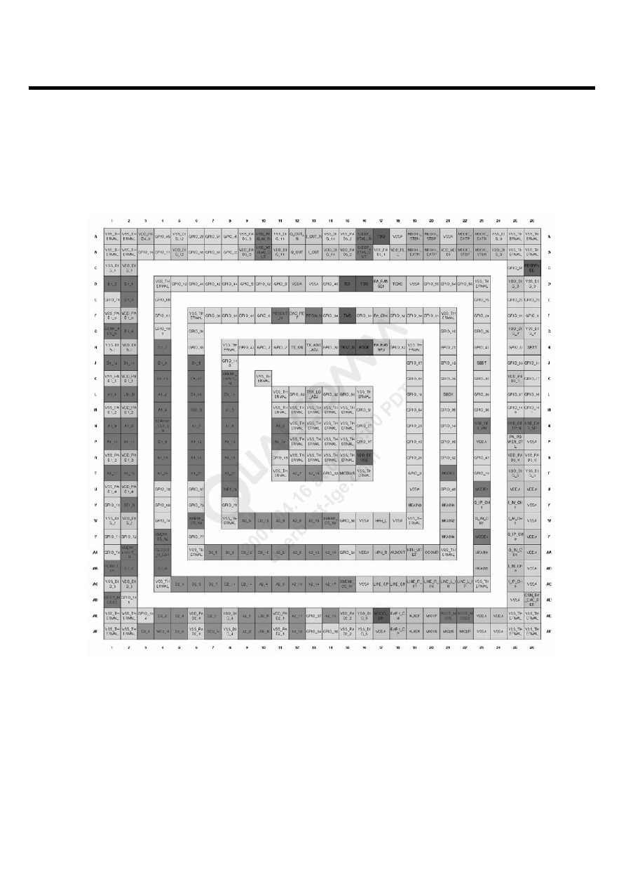
- 183 -
8. BGA IC PIN MAP
1. MSM6280
(Top View)
8. BGA IC PIN MAP
LGE Internal Use Only
Copyright © 2007 LG Electronics. Inc. All right reserved.
Only for training and service purposes
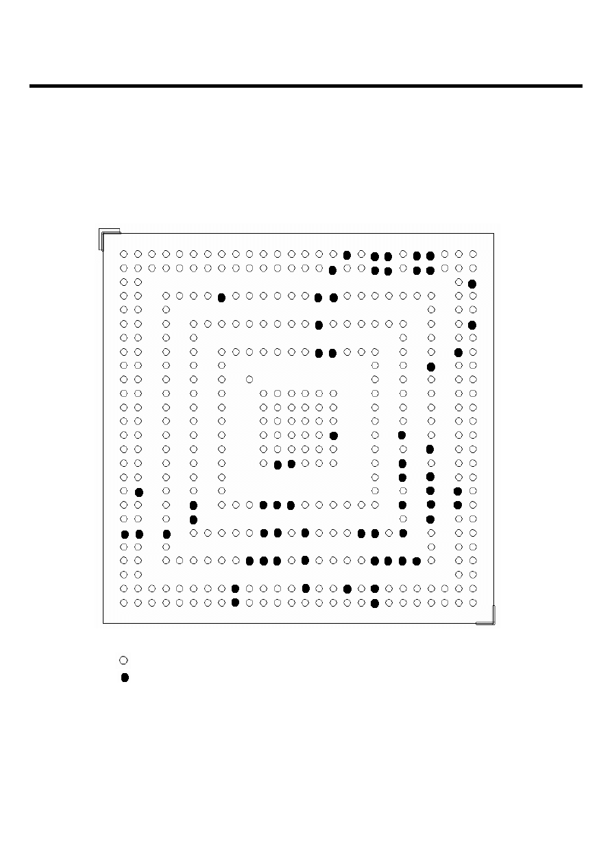
- 184 -
8. BGA IC PIN MAP
1. MSM6280
(Top View)
LGE Internal Use Only
Copyright © 2007 LG Electronics. Inc. All right reserved.
Only for training and service purposes
1 2 3 4 5 6 7 8 9
10 11 12 13 14 15 16 17 18 19 20 21 22 23 24 25 26
A
B
C
D
E
F
G
H
J
K
L
M
N
P
R
T
U
V
W
Y
AA
AB
AC
AD
AE
AF
A
B
C
D
E
F
G
H
J
K
L
M
N
P
R
T
U
V
W
Y
AA
AB
AC
AD
AE
AF
1 2 3 4 5 6 7 8 9
10 11 12 13 14 15 16 17 18 19 20 21 22 23 24 25 26
Not used
Used
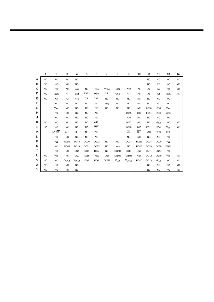
- 185 -
8. BGA IC PIN MAP
2. MCP (Top View)
LGE Internal Use Only
Copyright © 2007 LG Electronics. Inc. All right reserved.
Only for training and service purposes
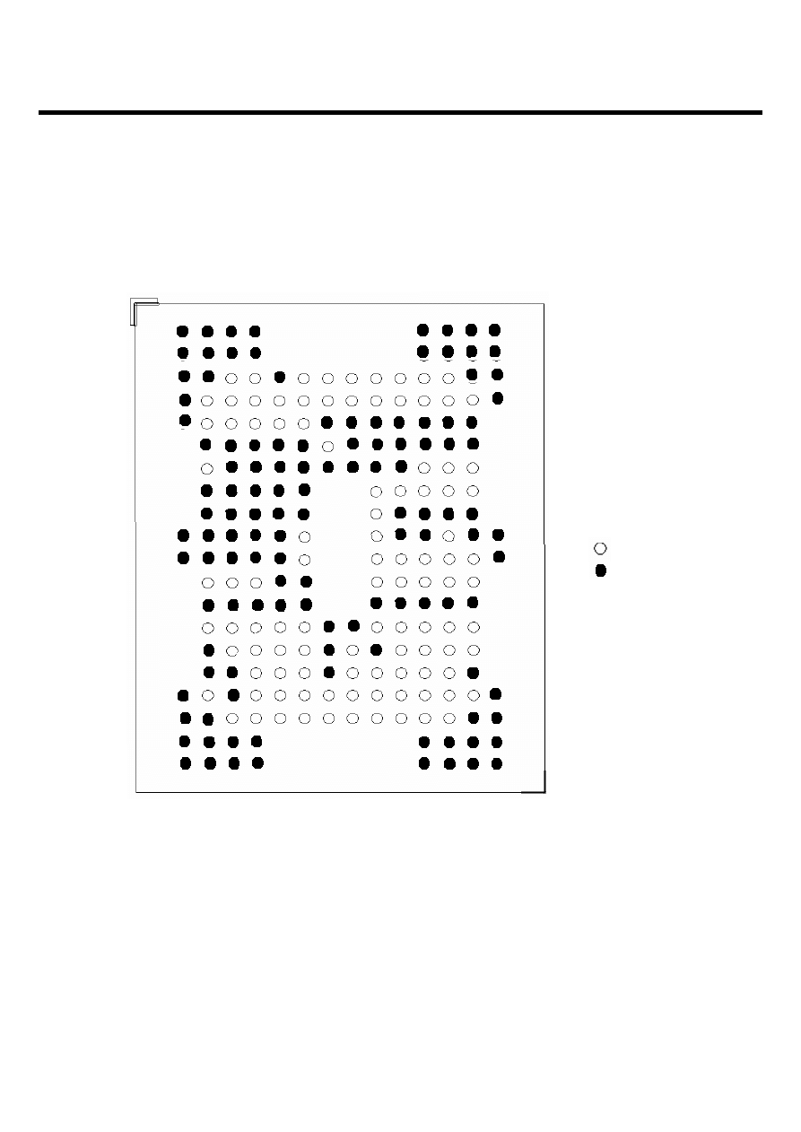
- 186 -
8. BGA IC PIN MAP
2. MCP (Top View)
LGE Internal Use Only
Copyright © 2007 LG Electronics. Inc. All right reserved.
Only for training and service purposes
Not used
Used
1 2 3 4 5 6 7 8 9
10 11 12 13 14
A
B
C
D
E
F
G
H
J
K
L
M
N
P
R
T
U
V
W
Y
1 2 3 4 5 6 7 8 9
10 11 12 13 14
A
B
C
D
E
F
G
H
J
K
L
M
N
P
R
T
U
V
W
Y
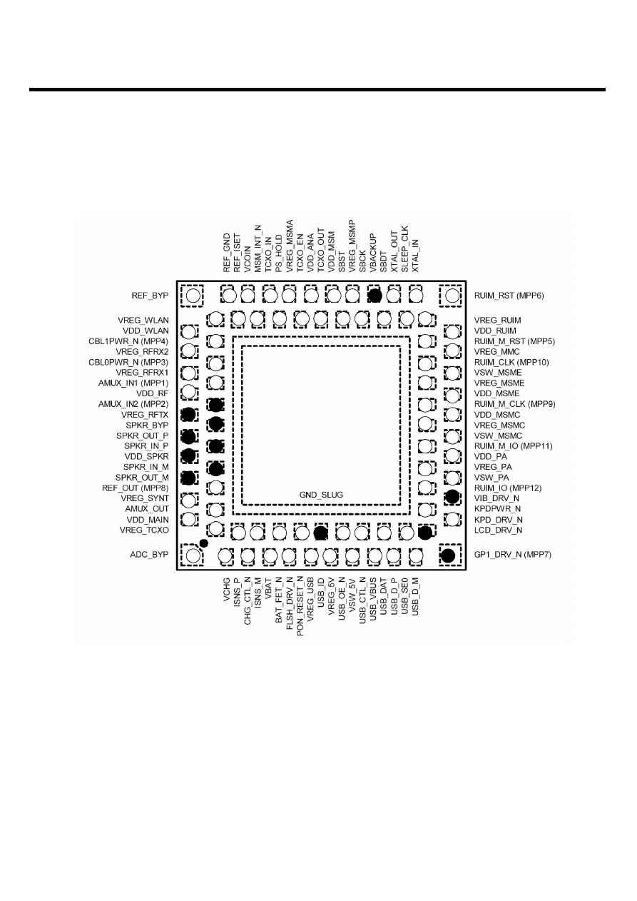
- 187 -
8. BGA IC PIN MAP
3. PM6650-2 (PMIC)
LGE Internal Use Only
Copyright © 2007 LG Electronics. Inc. All right reserved.
Only for training and service purposes
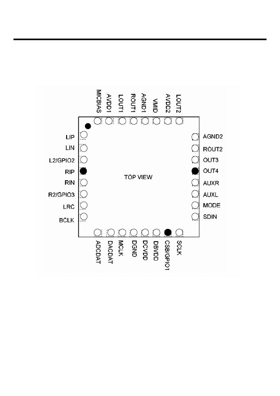
- 188 -
8. BGA IC PIN MAP
4. WM8983 (Audio codec)
LGE Internal Use Only
Copyright © 2007 LG Electronics. Inc. All right reserved.
Only for training and service purposes
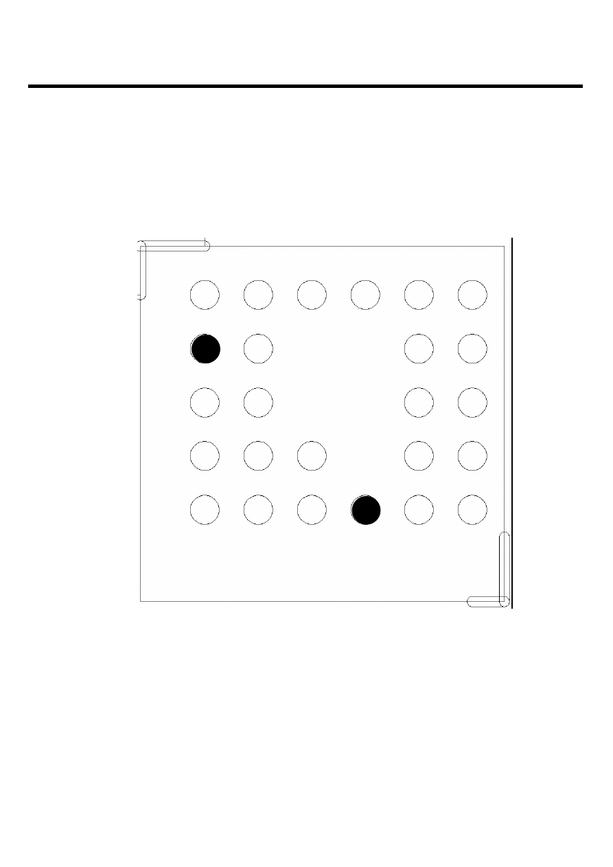
- 189 -
8. BGA IC PIN MAP
5. FM RADIO
LGE Internal Use Only
Copyright © 2007 LG Electronics. Inc. All right reserved.
Only for training and service purposes
A
B
C
D
E
1
2
3
4
5
6
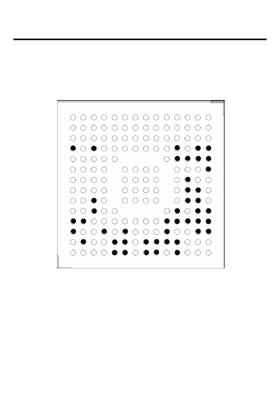
- 190 -
8. BGA IC PIN MAP
LGE Internal Use Only
Copyright © 2007 LG Electronics. Inc. All right reserved.
Only for training and service purposes
6. ZORAN(ZR3453)
A
B
C
D
E
F
G
H
J
K
L
M
N
1
2
3
4
5
6
7
8
9
10
11
12
13
14
P
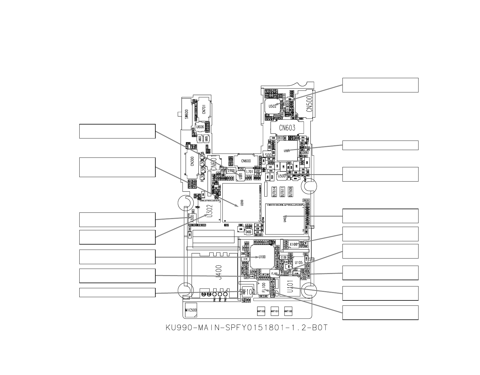
- 191 -
LGE Internal Use Only
9. PCB LAYOUT
Copyright © 2007 LG Electronics. Inc. All right reserved.
Only for training and service purposes
<LDO IC>
- 1.0V, 1.2V power supply
<Xtal>
- Check the frequency (27MHz)
<Multi media IC>
- Camcorder, Camera operation
<RF IC>
- GSM, WCDMA TX/RX operation
<UMTS RX SAW filter>
- WCDMA RX operation
<RF SW>
<Baseband and RF IC>
- Check the battery voltage and
Outputs of LDOs-Rx operation
<Charging IC>
- Check the TA and bettery
<Audio Codec>
- Headset, speaker operation
<Memory IC>- Check S/W
download
<Xtal>- Check the frequency
(19.2MHz)
<GSM900 TX SAW filter>
- GSM900 TX operation
<UMTS Duplexer>
- WCDMA RX,TX separation
<GSM PAM>- GSM TX
amplifier operation
<FEM>- RX, TX
switching selection
<PM IC>- Power management
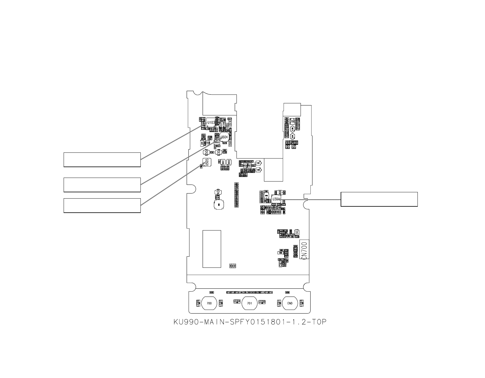
- 192 -
LGE Internal Use Only
Copyright © 2007 LG Electronics. Inc. All right reserved.
Only for training and service purposes
9. PCB LAYOUT
<FM radio IC>
- FM radio operation
<Headphone AMP>
- Headset operation
<OVP IC>
- Over voltage protection
<Charge Pump>
- LCD backlight charge pump
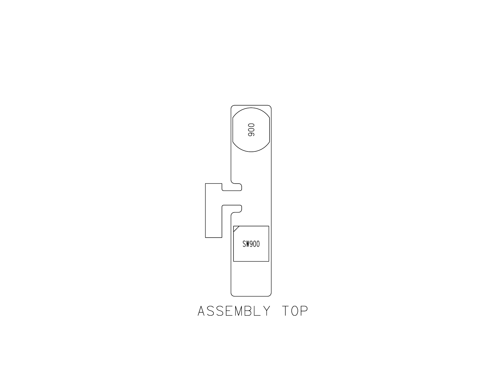
- 193 -
LGE Internal Use Only
Copyright © 2007 LG Electronics. Inc. All right reserved.
Only for training and service purposes
9. PCB LAYOUT
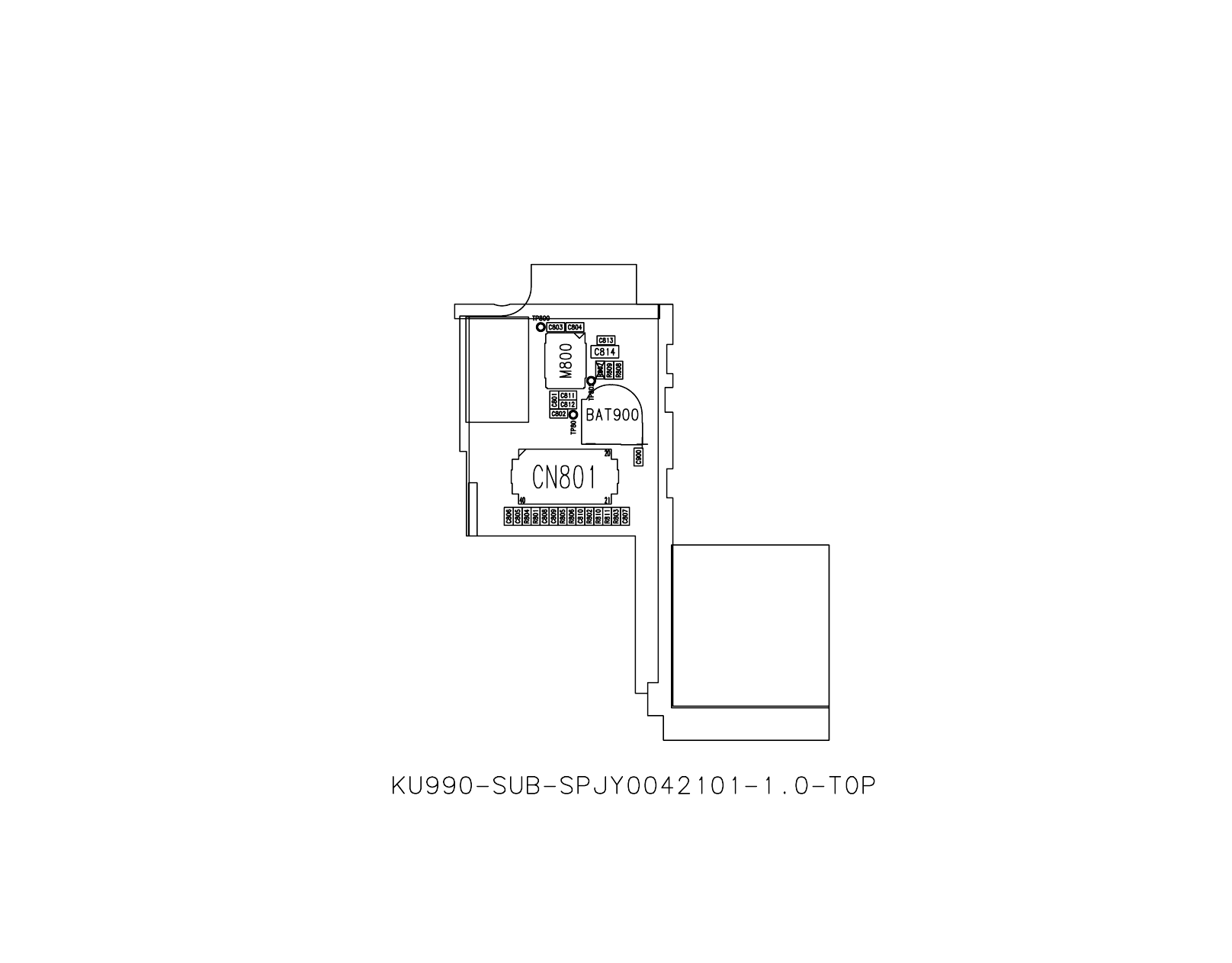
- 194 -
LGE Internal Use Only
Copyright © 2007 LG Electronics. Inc. All right reserved.
Only for training and service purposes
9. PCB LAYOUT
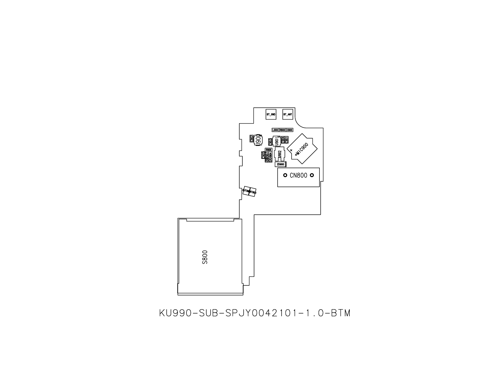
- 195 -
LGE Internal Use Only
Copyright © 2007 LG Electronics. Inc. All right reserved.
Only for training and service purposes
9. PCB LAYOUT
- 196 -
LGE Internal Use Only
Copyright © 2007 LG Electronics. Inc. All right reserved.
Only for training and service purposes
9. PCB LAYOUT
- 197 -
LGE Internal Use Only
Copyright © 2007 LG Electronics. Inc. All right reserved.
Only for training and service purposes
9. PCB LAYOUT

- 198 -
LGE Internal Use Only
Copyright © 2007 LG Electronics. Inc. All right reserved.
Only for training and service purposes
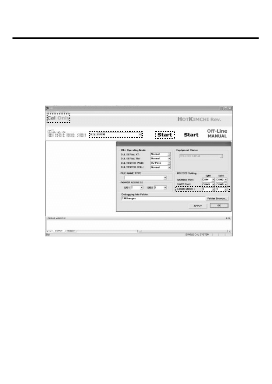
LGE Internal Use Only
Copyright © 2007 LG Electronics. Inc. All right reserved.
Only for training and service purposes
10. Calibration
- 199 -
10. Calibration
10.1 Usage of Hot-Kimchi
10.1.1 Calibration
• Procedure
1. Click SETTING in menu, and logic operation in sub-menu.
Choose “1” in LOGIC MODE (means calibration alone)
2.Select the model name which you want in list box
3.Click Start button to calibrate a phone
Model Name
Calibration only
- 200 -
10. Calibration
10.1.2 Basic Setting
• Contents
√ Click SETTING in menu, and logic operation in sub-menu.
√ You can select how to control AT comm, Testset, and Power supply in DLL Operating Mode.
√ You can set UART Port and logic mode. (mode 1 : Calibration alone)
√ You can set Result File’s name type. If you choose “TIME”, the saved files’ name is saved in a run -
time.
√ You can run the multi mode (S/B1,S/B2 : You can use S/B1 for only one port.)
√ You can set the path of HOTKIMCHI program.
LGE Internal Use Only
Copyright © 2007 LG Electronics. Inc. All right reserved.
Only for training and service purposes
- 201 -
10. Calibration
10.1.3 Log of Calibration and Test
• Contents
√ On Running, Log window is created in center area. It displays logs of command, and measurements
of Calibration or Autotest.
√ The result files are saved in the directory “~janghee\debug\Cal”, “~janghee\debug\Auto”, or
“~janghee\debug\CalAuto”.
LGE Internal Use Only
Copyright © 2007 LG Electronics. Inc. All right reserved.
Only for training and service purposes

- 202 -
LGE Internal Use Only
Copyright © 2007 LG Electronics. Inc. All right reserved.
Only for training and service purposes
- 203 -
1
2
87
4
90 4
6
7
8
9
14 15 20
19
18
23
21
17
24 25
29 30 31
32
33 36
37
38
39
40
41
42
35
34
28
27
26
22
13
12
11
10
16
57
56
54
53
52
51
89
71
72
73
74
82
83
85
84
55 59 60 65 66
67
68 69 70
50
48
86
3
46
49
47
43
45
44
58
61 62
63 64
88
75
76 77 78 79
81
80
11. EXPLODED VIEW & REPLACEMENT PART LIST
11.1 EXPLODED VIEW
LGE Internal Use Only
Copyright © 2007 LG Electronics. Inc. All right reserved.
Only for training and service purposes
- 204 -
LGE Internal Use Only
Copyright © 2007 LG Electronics. Inc. All right reserved.
Only for training and service purposes
A
B
C
D
ASS'Y EXPLODED VIEW
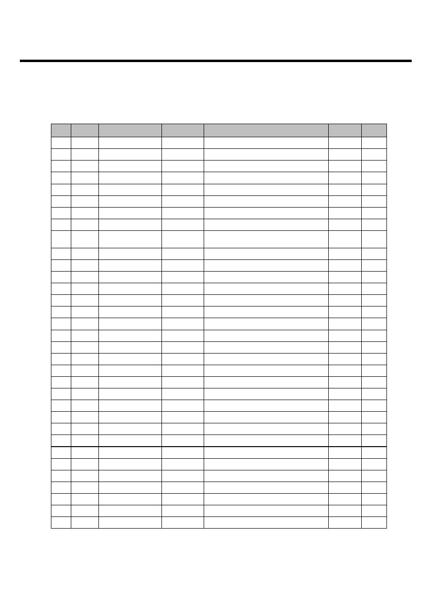
LGE Internal Use Only
Copyright © 2007 LG Electronics. Inc. All right reserved.
Only for training and service purposes
11. EXPLODED VIEW & REPLACEMENT PART LIST
- 205 -
11.2 Replacement Parts
<Mechanic component>
Note: This Chapter is used for reference, Part order
is ordered by SBOM standard on GCSC
Level
Location
No.
Description
Part Number
Spec
Color
Remark
1
IMT,BAR/FLIP
TIMT0000711
Black
2
AAAY00
ADDITION
AAAY0260102
Without Color
3
WSAY00
SOFTWARE,APPLICATION
WSAY0113601
; , , ,WORLD WIDE , ,
3
MCCL00
CAP,BOX
MCCL0001103
BOX, TW, , , , ,
Without Color
3
MCJZ00
COVER
MCJZ0049101
BOX, TW, , , , ,
Without Color
3
MLAC00
LABEL,BARCODE
MLAC0004501
Export(105*40)
Without Color
3
MLAJ00
LABEL,MASTER BOX
MLAJ0004401
LABEL,MASTER BOX(for C1300i NEW_CGR)
Without Color
3
MLAP00
LABEL,UNIT
MLAP0001115
Reliance Seal Label
Without Color
3
MPAA00
PACKING,BLISTER(LOWE
R)
MPAA0002003
PRESS, PB, , , , ,
Without Color
3
MPAB00
PACKING,BLISTER(UPPER
)
MPAB0001603
PRESS, PB, , , , ,
Without Color
3
MPCY00
PALLET
MPCY0011201
PALLET(for G5400 O2U 1200x1000_Wooden)
Silver
2
APEY00
PHONE
APEY0415111
Black
3
ACGK00
COVER ASSY,FRONT
ACGK0093401
Without Color
4
ACGZ00
COVER ASSY
ACGZ0013901
UPPER
Without Color
5
MCJZ00
COVER
MCJZ0046501
MOLD, PC LUPOY SC-1004A, , , , ,
Black
5
6
MICA01
INSERT,FRONT
MICA0013901
2.2X4.0
Without Color
9
5
MFBB00
FILTER,RECEIVER
MFBB0023201
COMPLEX, (empty), , , , ,
Without Color
4
5
MPBM00
PAD,RECEIVER
MPBM0019201
COMPLEX, (empty), , , , ,
Without Color
7
5
MTAF
TAPE,MOTOR
MTAF0006001
Without Color
6
5
MTAK00
TAPE,CAMERA
MTAK0002501
COMPLEX, (empty), , , , ,
Without Color
8
4
ACHA00
COVER SUB ASSY,FRONT
ACHA0001801
Without Color
5
MBJL00
BUTTON,SIDE
MBJL0042701
MOLD, ABS MP-211, , , , ,
Silver
27
5
MCCC00
CAP,EARPHONE JACK
MCCC0045901
COMPLEX, (empty), , , , ,
Black
`4
5
MCJK00
COVER,FRONT
MCJK0073001
MOLD, PC LUPOY SC-1004A, , , , ,
Black
22
6
MICA00
INSERT,FRONT
MICA0019901
M1.4 D2.2 L1.5
Gold
34
5
MDAG00
DECO,FRONT
MDAG0028401
MOLD, PC LUPOY SC-1004A, , , , ,
Black
17
5
MKBZ00
KNOB
MKBZ0002101
MOLD, PC LUPOY SC-1004A, , , , ,
Black
25
5
MLEA00
LOCKER,BATTERY
MLEA0039301
MOLD, PC LUPOY SC-1004A, , , , ,
Black
18
5
MPBT00
PAD,CAMERA
MPBT0044701
COMPLEX, (empty), , , , ,
Without Color
33
5
MSDC00
SPRING,LOCKER
MSDC0010601
Without Color
19
5
MSIY00
SHAFT
MSIY0001201
CUTTING, STS, , , , ,
Silver
29
5
MTAA00
TAPE,DECO
MTAA0142501
COMPLEX, (empty), , , , ,
Without Color
23
5
MTAA01
TAPE,DECO
MTAA0142601
COMPLEX, (empty), , , , ,
Without Color
21
LGE Internal Use Only
Copyright © 2007 LG Electronics. Inc. All right reserved.
Only for training and service purposes
11. EXPLODED VIEW & REPLACEMENT PART LIST
- 206 -
Level
Location
No.
Description
Part Number
Spec
Color
Remark
5
MTAA02
TAPE,DECO
MTAA0142701
COMPLEX, (empty), , , , ,
Without Color
20
5
MTAA03
TAPE,DECO
MTAA0142801
COMPLEX, (empty), , , , ,
Without Color
16
5
MTAA04
TAPE,DECO
MTAA0146601
COMPLEX, (empty), , , , ,
Without Color
26
5
MTAB00
TAPE,PROTECTION
MTAB0185401
COMPLEX, (empty), , , , ,
Without Color
28
5
MTAC00
TAPE,SHIELD
MTAC0057901
COMPLEX, (empty), , , , ,
Without Color
32
5
MTAC01
TAPE,SHIELD
MTAC0058101
COMPLEX, (empty), , , , ,
Without Color
31
5
MTAZ00
TAPE
MTAZ0193901
COMPLEX, (empty), , , , ,
Black
11
5
MTAZ01
TAPE
MTAZ0195701
COMPLEX, (empty), , , , ,
Without Color
12
5
MTAZ02
TAPE
MTAZ0195801
COMPLEX, (empty), , , , ,
Without Color
15
5
MTAZ03
TAPE
MTAZ0195901
COMPLEX, (empty), , , , ,
Without Color
24
4
MKAG00
KEYPAD,MAIN
MKAG0000901
MOLD, PC LUPOY SC-1004A, , , , ,
Black
35
4
MLAZ00
LABEL
MLAZ0038303
PRINTING, (empty), , , , ,
White
4
MPBG00
PAD,LCD
MPBG0065101
COMPLEX, (empty), , , , ,
Black
4
MPBG01
PAD,LCD
MPBG0068901
COMPLEX, (empty), , , , ,
Without Color
4
MPBT00
PAD,CAMERA
MPBT0044901
COMPLEX, (empty), , , , ,
Without Color
38
4
MPBZ00
PAD
MPBZ0193801
COMPLEX, (empty), , , , ,
Without Color
4
MTAB00
TAPE,PROTECTION
MTAB0182801
COMPLEX, (empty), , , , ,
Without Color
1
4
MTAB01
TAPE,PROTECTION
MTAB0182901
COMPLEX, (empty), , , , ,
Without Color
3
4
MTAC00
TAPE,SHIELD
MTAC0058201
COMPLEX, (empty), , , , ,
Without Color
4
MTAD00
TAPE,WINDOW
MTAD0072001
COMPLEX, (empty), , , , ,
Without Color
4
MWAC00
WINDOW,LCD
MWAC0083101
COMPLEX, (empty), , , , ,
Without Color
4
SACY00
PCB ASSY,FLEXIBLE
SACY0063001
5
SACE00
PCB ASSY,FLEXIBLE,SMT
SACE0057301
6
SACC00
PCB ASSY,FLEXIBLE,SMT
BOTTOM
SACC0036101
7
ENBY00
CONNECTOR,BOARD TO
BOARD
ENBY0018601
10 PIN,.4 mm,STRAIGHT , ,H=0.9, SOCKET
6
SACD00
PCB ASSY,FLEXIBLE,SMT
TOP
SACD0047101
7
ENBY00
CONNECTOR,BOARD TO
BOARD
ENBY0019501
20 PIN,.4 mm,ETC , ,H=1.5, Socket
7
ENBY01
CONNECTOR,BOARD TO
BOARD
ENBY0040601
30 PIN,0.4 mm,ETC , ,H=1.0 ,; , ,0.40MM ,STRAIGHT
,MALE ,SMD ,R/TP , ,
6
SPCY00
PCB,FLEXIBLE
SPCY0106101
POLYI ,0.4 mm,Mutil-5,VGA-CAM ,; , , , , , , , , ,
4
SJMY00
VIBRATOR,MOTOR
SJMY0008502
3 V,1.0 A,10*3.6T ,2.0Vrms 175HZ linear motor 1.5G ,;
,3V , , ,1.5G , , , ,
36
4
SURY00
RECEIVER
SURY0012801
37
4
SVCY00
CAMERA
SVCY0014601
CMOS ,MEGA ,5M AF, Sony 1/2.8", HPCB
39
4
SVCY01
CAMERA
SVCY0014001
CMOS ,VGA ,5.5x11.4x3.2t, Magna 1/7.4"
LGE Internal Use Only
Copyright © 2007 LG Electronics. Inc. All right reserved.
Only for training and service purposes
11. EXPLODED VIEW & REPLACEMENT PART LIST
- 207 -
Level
Location
No.
Description
Part Number
Spec
Color
Remark
4
SVLM00
LCD MODULE
SVLM0025501
MAIN ,240*400 ,45.08*75*2.2 ,262k ,TFT ,TM ,DAC
IC(Sharp) ,
10
3
ACGM00
COVER ASSY,REAR
ACGM0094701
Without Color
4
ENZY00
CONNECTOR,ETC
ENZY0019901
3 PIN,3 mm,STRAIGHT , ,
70
4
ESQY00
SWITCH,ROTARY
ESQY0001201
6 V,0.005 A,HORIZONTAL ,0.04 G,KU990 Wheel Switch
,; ,2C2P ,6VDC ,0.5MA ,HORIZONTAL ,
81
4
MCJN00
COVER,REAR
MCJN0069201
MOLD, PC LUPOY SC-1004A, , , , ,
Black
75
4
MDAD00
DECO,CAMERA
MDAD0032801
PRESS, Al, 0.3, , , ,
Black
80
4
MFBC00
FILTER,SPEAKER
MFBC0033001
COMPLEX, (empty), , , , ,
Without Color
64
4
MFBD00
FILTER,MIKE
MFBD0025301
COMPLEX, (empty), , , , ,
Without Color
74
4
MFBD01
FILTER,MIKE
MFBD0025401
COMPLEX, (empty), , , , ,
Black
62
4
MLAB00
LABEL,A/S
MLAB0001102
C2000 USASV DIA 4.0
White
4
MPBH00
PAD,MIKE
MPBH0032201
COMPLEX, (empty), , , , ,
Without Color
57,71
4
MPBH01
PAD,MIKE
MPBH0032301
COMPLEX, (empty), , , , ,
Without Color
4
MPBH02
PAD,MIKE
MPBH0032401
COMPLEX, (empty), , , , ,
Without Color
72
4
MPBM00
PAD,RECEIVER
MPBM0019401
COMPLEX, (empty), , , , ,
Without Color
59
4
MPBT00
PAD,CAMERA
MPBT0044801
COMPLEX, (empty), , , , ,
Without Color
4
MPBU00
PAD,CONNECTOR
MPBU0007601
COMPLEX, (empty), , , , ,
Without Color
56
4
MPBU01
PAD,CONNECTOR
MPBU0007701
COMPLEX, (empty), , , , ,
Without Color
68
4
MPBZ00
PAD
MPBZ0187301
COMPLEX, (empty), , , , ,
Without Color
76
4
MPFZ01
PLATE
MPFZ0029901
COMPLEX, (empty), , , , ,
Without Color
82
4
MSDD00
SPRING,PLATE
MSDD0006701
PRESS, Bs, 0.15, , , ,
Gold
66
4
MSDD01
SPRING,PLATE
MSDD0006901
PRESS, Bs, , , , ,
Gold
63
4
MTAA00
TAPE,DECO
MTAA0142901
COMPLEX, (empty), , , , ,
Without Color
79
4
MTAC00
TAPE,SHIELD
MTAC0058301
COMPLEX, (empty), , , , ,
Without Color
69
4
MTAD00
TAPE,WINDOW
MTAD0072101
COMPLEX, (empty), , , , ,
Without Color
77
4
MTAJ00
TAPE,FLEXIBLE PCB
MTAJ0001701
COMPLEX, (empty), , , , ,
Without Color
60
4
MTAZ00
TAPE
MTAZ0194001
COMPLEX, (empty), , , , ,
Without Color
47
4
MTAZ01
TAPE
MTAZ0197401
COMPLEX, (empty), 0.1, , , ,
Without Color
65
4
MWAE00
WINDOW,CAMERA
MWAE0028001
CUTTING, Quartz Glass, , , , ,
Without Color
78
4
MWAE01
WINDOW,CAMERA
MWAE0026401
MOLD, Polyarylamide IXEF 1032, , , , ,
Without Color
67
3
MLAK00
LABEL,MODEL
MLAK0006901
5
MLAZ00
LABEL
MLAZ0038301
PID Label 4 Array
Without Color
LGE Internal Use Only
Copyright © 2007 LG Electronics. Inc. All right reserved.
Only for training and service purposes
11. EXPLODED VIEW & REPLACEMENT PART LIST
- 208 -
Level
Location
No.
Description
Part Number
Spec
Color
Remark
4
SNGF00
ANTENNA,GSM,FIXED
SNGF0027102
3.0 ,-2.0 dBd, ,EGSM+DCS+PCS+W-BAND I, INTERNAL
,; ,QUAD ,-2.0 ,50 ,3.0
58,73
4
SNGF01
ANTENNA,GSM,FIXED
SNGF0027201
3.0 ,-2.0 dBd, ,BLUETOOTH, INTERNAL ,; ,SINGLE ,-2.0
,50 ,3.0
3
GMEY00
SCREW MACHINE,BIND
GMEY0010601
1.4 mm,2.5 mm,MSWR3(BK) ,N ,+ ,NYLOK
Black
84
3
SACY00
PCB ASSY,FLEXIBLE
SACY0063003
4
SACE00
PCB ASSY,FLEXIBLE,SMT
SACE0057302
5
SACD00
PCB ASSY,FLEXIBLE,SMT
TOP
SACD0047102
6
CN601
CONNECTOR,BOARD TO
BOARD
ENBY0041601
28 PIN,0.4 mm,ETC , ,B to B ,; , ,0.40MM ,[empty] ,MALE
,SMD ,BK , ,
6
ENBY01
CONNECTOR,BOARD TO
BOARD
ENBY0040601
30 PIN,0.4 mm,ETC , ,H=1.0 ,; , ,0.40MM ,STRAIGHT
,MALE ,SMD ,R/TP , ,
5
SPCY00
PCB,FLEXIBLE
SPCY0103601
POLYI ,0.2 mm,DOUBLE ,5M-F-CAM ,; , , , , , , , , ,
3
SAFY00
PCB ASSY,MAIN
SAFY0203411
44
4
SAFB00
PCB ASSY,MAIN,INSERT
SAFB0075601
5
ADCA00
DOME ASSY,METAL
ADCA0069301
Without Color
43
5
SPKY00
PCB,SIDEKEY
SPKY0049301
POLYI ,0.2 mm,DOUBLE , ,; , , , , , , , , ,
4
SAFF00
PCB ASSY,MAIN,SMT
SAFF0124311
5
SAFC00
PCB ASSY,MAIN,SMT
BOTTOM
SAFC0091501
6
C100
CAP,CERAMIC,CHIP
ECCH0001002
180 pF,50V ,J ,NP0 ,TC ,1005 ,R/TP
6
C101
CAP,CERAMIC,CHIP
ECCH0000129
120 pF,50V,J,NP0,TC,1005,R/TP
6
C102
INDUCTOR,CHIP
ELCH0001401
15 nH,J ,1005 ,R/TP ,Pb Free
6
C103
CAP,CERAMIC,CHIP
ECCH0001002
180 pF,50V ,J ,NP0 ,TC ,1005 ,R/TP
6
C104
CAP,CERAMIC,CHIP
ECCH0000196
0.75 pF,50V ,C ,NP0 ,TC ,1005 ,R/TP
6
C105
CAP,CHIP,MAKER
ECZH0000841
56 pF,50V ,J ,NP0 ,TC ,1005 ,R/TP
6
C106
CAP,CERAMIC,CHIP
ECCH0000107
6 pF,50V,D,NP0,TC,1005,R/TP
6
C107
CAP,CERAMIC,CHIP
ECCH0001002
180 pF,50V ,J ,NP0 ,TC ,1005 ,R/TP
6
C108
CAP,CHIP,MAKER
ECZH0000806
5 pF,50V ,C ,NP0 ,TC ,1005 ,R/TP
6
C110
CAP,CERAMIC,CHIP
ECCH0001002
180 pF,50V ,J ,NP0 ,TC ,1005 ,R/TP
6
C111
CAP,CERAMIC,CHIP
ECCH0000149
3.3 nF,50V,K,X7R,HD,1005,R/TP
6
C112
CAP,CERAMIC,CHIP
ECCH0000143
1 nF,50V,K,X7R,HD,1005,R/TP
6
C116
CAP,CHIP,MAKER
ECZH0000816
12 pF,50V ,J ,NP0 ,TC ,1005 ,R/TP
6
C117
CAP,CERAMIC,CHIP
ECCH0000115
22 pF,50V,J,NP0,TC,1005,R/TP
6
C118
CAP,CERAMIC,CHIP
ECCH0000393
22 uF,6.3V ,M ,X5R ,HD ,2012 ,R/TP
11.2 Replacement Parts
<Main component>
Note: This Chapter is used for reference, Part order
is ordered by SBOM standard on GCSC
LGE Internal Use Only
Copyright © 2007 LG Electronics. Inc. All right reserved.
Only for training and service purposes
11. EXPLODED VIEW & REPLACEMENT PART LIST
- 209 -
Level
Location
No.
Description
Part Number
Spec
Color
Remark
6
C119
CAP,CERAMIC,CHIP
ECCH0000182
0.1 uF,10V ,K ,X5R ,HD ,1005 ,R/TP
6
C120
CAP,CERAMIC,CHIP
ECCH0000182
0.1 uF,10V ,K ,X5R ,HD ,1005 ,R/TP
6
C121
CAP,CERAMIC,CHIP
ECCH0000182
0.1 uF,10V ,K ,X5R ,HD ,1005 ,R/TP
6
C122
CAP,CERAMIC,CHIP
ECCH0000182
0.1 uF,10V ,K ,X5R ,HD ,1005 ,R/TP
6
C123
CAP,CERAMIC,CHIP
ECCH0000182
0.1 uF,10V ,K ,X5R ,HD ,1005 ,R/TP
6
C124
CAP,CERAMIC,CHIP
ECCH0000182
0.1 uF,10V ,K ,X5R ,HD ,1005 ,R/TP
6
C125
CAP,CERAMIC,CHIP
ECCH0004904
1 uF,6.3V ,K ,X5R ,TC ,1005 ,R/TP
6
C126
CAP,CERAMIC,CHIP
ECCH0000115
22 pF,50V,J,NP0,TC,1005,R/TP
6
C127
CAP,CHIP,MAKER
ECZH0000813
100 pF,50V ,J ,NP0 ,TC ,1005 ,R/TP
6
C128
CAP,CERAMIC,CHIP
ECCH0000115
22 pF,50V,J,NP0,TC,1005,R/TP
6
C129
CAP,CERAMIC,CHIP
ECCH0000182
0.1 uF,10V ,K ,X5R ,HD ,1005 ,R/TP
6
C130
CAP,CERAMIC,CHIP
ECCH0000393
22 uF,6.3V ,M ,X5R ,HD ,2012 ,R/TP
6
C131
CAP,CHIP,MAKER
ECZH0000813
100 pF,50V ,J ,NP0 ,TC ,1005 ,R/TP
6
C132
CAP,CERAMIC,CHIP
ECCH0000155
10 nF,16V,K,X7R,HD,1005,R/TP
6
C133
CAP,CERAMIC,CHIP
ECCH0000115
22 pF,50V,J,NP0,TC,1005,R/TP
6
C134
CAP,CERAMIC,CHIP
ECCH0000143
1 nF,50V,K,X7R,HD,1005,R/TP
6
C135
CAP,TANTAL,CHIP
ECTH0005501
33 uF,10V ,M ,L_ESR ,2012 ,R/TP ,; , ,[empty] ,[empty] ,
,-55TO+125C , ,[empty] ,[empty] ,[empty] ,[empty]
6
C136
CAP,CERAMIC,CHIP
ECCH0000109
8 pF,50V,D,NP0,TC,1005,R/TP
6
C137
CAP,CERAMIC,CHIP
ECCH0004904
1 uF,6.3V ,K ,X5R ,TC ,1005 ,R/TP
6
C139
CAP,CERAMIC,CHIP
ECCH0000182
0.1 uF,10V ,K ,X5R ,HD ,1005 ,R/TP
6
C140
CAP,CERAMIC,CHIP
ECCH0000143
1 nF,50V,K,X7R,HD,1005,R/TP
6
C141
CAP,CERAMIC,CHIP
ECCH0000155
10 nF,16V,K,X7R,HD,1005,R/TP
6
C142
CAP,CERAMIC,CHIP
ECCH0000196
0.75 pF,50V ,C ,NP0 ,TC ,1005 ,R/TP
6
C143
CAP,CHIP,MAKER
ECZH0000844
68 pF,50V ,J ,NP0 ,TC ,1005 ,R/TP
6
C144
CAP,CERAMIC,CHIP
ECCH0000143
1 nF,50V,K,X7R,HD,1005,R/TP
6
C145
CAP,CERAMIC,CHIP
ECCH0000143
1 nF,50V,K,X7R,HD,1005,R/TP
6
C146
CAP,CERAMIC,CHIP
ECCH0000110
10 pF,50V,D,NP0,TC,1005,R/TP
6
C147
CAP,CERAMIC,CHIP
ECCH0000143
1 nF,50V,K,X7R,HD,1005,R/TP
6
C148
CAP,CHIP,MAKER
ECZH0001105
8200 pF,16V ,K ,X7R ,HD ,1005 ,R/TP
6
C149
CAP,CERAMIC,CHIP
ECCH0000115
22 pF,50V,J,NP0,TC,1005,R/TP
6
C152
CAP,CERAMIC,CHIP
ECCH0000195
3.9 pF,50V ,C ,NP0 ,TC ,1005 ,R/TP
6
C153
CAP,CHIP,MAKER
ECZH0000841
56 pF,50V ,J ,NP0 ,TC ,1005 ,R/TP
6
C154
CAP,CHIP,MAKER
ECZH0000841
56 pF,50V ,J ,NP0 ,TC ,1005 ,R/TP
6
C155
CAP,CERAMIC,CHIP
ECCH0000101
.5 pF,50V ,C ,NP0 ,TC ,1005 ,R/TP
6
C156
CAP,CERAMIC,CHIP
ECCH0000901
2.2 pF,50V ,C ,NP0 ,TC ,1005 ,R/TP
6
C159
CAP,CHIP,MAKER
ECZH0000846
8.2 pF,50V ,C ,NP0 ,TC ,1005 ,R/TP
LGE Internal Use Only
Copyright © 2007 LG Electronics. Inc. All right reserved.
Only for training and service purposes
11. EXPLODED VIEW & REPLACEMENT PART LIST
- 210 -
Level
Location
No.
Description
Part Number
Spec
Color
Remark
6
C160
CAP,TANTAL,CHIP
ECTH0004101
22 uF,6.3V ,M ,STD ,1608 ,R/TP
6
C161
CAP,CHIP,MAKER
ECZH0000841
56 pF,50V ,J ,NP0 ,TC ,1005 ,R/TP
6
C162
CAP,CERAMIC,CHIP
ECCH0000155
10 nF,16V,K,X7R,HD,1005,R/TP
6
C163
CAP,CHIP,MAKER
ECZH0000813
100 pF,50V ,J ,NP0 ,TC ,1005 ,R/TP
6
C164
CAP,CERAMIC,CHIP
ECCH0004904
1 uF,6.3V ,K ,X5R ,TC ,1005 ,R/TP
6
C167
CAP,CHIP,MAKER
ECZH0000841
56 pF,50V ,J ,NP0 ,TC ,1005 ,R/TP
6
C168
CAP,CHIP,MAKER
ECZH0000841
56 pF,50V ,J ,NP0 ,TC ,1005 ,R/TP
6
C169
CAP,CERAMIC,CHIP
ECCH0000185
5.6 pF,50V ,C ,NP0 ,TC ,1005 ,R/TP
6
C170
CAP,CERAMIC,CHIP
ECCH0000178
1.8 pF,50V ,D ,NP0 ,TC ,1005 ,R/TP
6
C173
CAP,CHIP,MAKER
ECZH0000813
100 pF,50V ,J ,NP0 ,TC ,1005 ,R/TP
6
C200
CAP,CERAMIC,CHIP
ECCH0000110
10 pF,50V,D,NP0,TC,1005,R/TP
6
C214
CAP,CERAMIC,CHIP
ECCH0000155
10 nF,16V,K,X7R,HD,1005,R/TP
6
C218
CAP,CERAMIC,CHIP
ECCH0000143
1 nF,50V,K,X7R,HD,1005,R/TP
6
C219
CAP,CERAMIC,CHIP
ECCH0000155
10 nF,16V,K,X7R,HD,1005,R/TP
6
C222
CAP,CERAMIC,CHIP
ECCH0000147
2.2 nF,50V,K,X7R,HD,1005,R/TP
6
C223
CAP,CERAMIC,CHIP
ECCH0000161
33 nF,16V,K,X7R,HD,1005,R/TP
6
C231
CAP,CERAMIC,CHIP
ECCH0000155
10 nF,16V,K,X7R,HD,1005,R/TP
6
C232
CAP,CERAMIC,CHIP
ECCH0000182
0.1 uF,10V ,K ,X5R ,HD ,1005 ,R/TP
6
C233
CAP,TANTAL,CHIP
ECTH0003701
10 uF,6.3V ,M ,L_ESR ,1608 ,R/TP
6
C235
CAP,CERAMIC,CHIP
ECCH0000182
0.1 uF,10V ,K ,X5R ,HD ,1005 ,R/TP
6
C236
CAP,CERAMIC,CHIP
ECCH0000182
0.1 uF,10V ,K ,X5R ,HD ,1005 ,R/TP
6
C238
CAP,CERAMIC,CHIP
ECCH0000182
0.1 uF,10V ,K ,X5R ,HD ,1005 ,R/TP
6
C239
CAP,TANTAL,CHIP,MAKER
ECTZ0004701
4.7 uF,6.3V ,M ,STD ,1608 ,R/TP
6
C300
CAP,TANTAL,CHIP
ECTH0003701
10 uF,6.3V ,M ,L_ESR ,1608 ,R/TP
6
C301
CAP,CERAMIC,CHIP
ECCH0000182
0.1 uF,10V ,K ,X5R ,HD ,1005 ,R/TP
6
C303
CAP,CERAMIC,CHIP
ECCH0000182
0.1 uF,10V ,K ,X5R ,HD ,1005 ,R/TP
6
C308
CAP,TANTAL,CHIP
ECTH0003701
10 uF,6.3V ,M ,L_ESR ,1608 ,R/TP
6
C309
CAP,TANTAL,CHIP
ECTH0003701
10 uF,6.3V ,M ,L_ESR ,1608 ,R/TP
6
C310
CAP,CERAMIC,CHIP
ECCH0000182
0.1 uF,10V ,K ,X5R ,HD ,1005 ,R/TP
6
C311
CAP,CERAMIC,CHIP
ECCH0000110
10 pF,50V,D,NP0,TC,1005,R/TP
6
C321
CAP,CERAMIC,CHIP
ECCH0000182
0.1 uF,10V ,K ,X5R ,HD ,1005 ,R/TP
6
C322
CAP,CERAMIC,CHIP
ECCH0000115
22 pF,50V,J,NP0,TC,1005,R/TP
6
C323
CAP,CERAMIC,CHIP
ECCH0000115
22 pF,50V,J,NP0,TC,1005,R/TP
6
C324
CAP,CERAMIC,CHIP
ECCH0000115
22 pF,50V,J,NP0,TC,1005,R/TP
6
C325
CAP,CERAMIC,CHIP
ECCH0000115
22 pF,50V,J,NP0,TC,1005,R/TP
6
C326
CAP,CERAMIC,CHIP
ECCH0000115
22 pF,50V,J,NP0,TC,1005,R/TP
6
C339
CAP,CERAMIC,CHIP
ECCH0000109
8 pF,50V,D,NP0,TC,1005,R/TP
LGE Internal Use Only
Copyright © 2007 LG Electronics. Inc. All right reserved.
Only for training and service purposes
11. EXPLODED VIEW & REPLACEMENT PART LIST
- 211 -
Level
Location
No.
Description
Part Number
Spec
Color
Remark
6
C340
CAP,CERAMIC,CHIP
ECCH0000109
8 pF,50V,D,NP0,TC,1005,R/TP
6
C403
CAP,CERAMIC,CHIP
ECCH0000182
0.1 uF,10V ,K ,X5R ,HD ,1005 ,R/TP
6
C404
CAP,CERAMIC,CHIP
ECCH0000182
0.1 uF,10V ,K ,X5R ,HD ,1005 ,R/TP
6
C405
CAP,CERAMIC,CHIP
ECCH0000182
0.1 uF,10V ,K ,X5R ,HD ,1005 ,R/TP
6
C406
CAP,CERAMIC,CHIP
ECCH0000182
0.1 uF,10V ,K ,X5R ,HD ,1005 ,R/TP
6
C407
CAP,CERAMIC,CHIP
ECCH0000182
0.1 uF,10V ,K ,X5R ,HD ,1005 ,R/TP
6
C408
CAP,CERAMIC,CHIP
ECCH0000182
0.1 uF,10V ,K ,X5R ,HD ,1005 ,R/TP
6
C409
CAP,CERAMIC,CHIP
ECCH0000182
0.1 uF,10V ,K ,X5R ,HD ,1005 ,R/TP
6
C410
CAP,CERAMIC,CHIP
ECCH0000155
10 nF,16V,K,X7R,HD,1005,R/TP
6
C411
CAP,CERAMIC,CHIP
ECCH0000182
0.1 uF,10V ,K ,X5R ,HD ,1005 ,R/TP
6
C500
CAP,TANTAL,CHIP
ECTH0005501
33 uF,10V ,M ,L_ESR ,2012 ,R/TP ,; , ,[empty] ,[empty] ,
,-55TO+125C , ,[empty] ,[empty] ,[empty] ,[empty]
6
C501
CAP,CERAMIC,CHIP
ECCH0000182
0.1 uF,10V ,K ,X5R ,HD ,1005 ,R/TP
6
C502
CAP,CERAMIC,CHIP
ECCH0000182
0.1 uF,10V ,K ,X5R ,HD ,1005 ,R/TP
6
C503
CAP,CERAMIC,CHIP
ECCH0000182
0.1 uF,10V ,K ,X5R ,HD ,1005 ,R/TP
6
C504
CAP,CERAMIC,CHIP
ECCH0006201
4.7 uF,6.3V ,K ,X5R ,TC ,1608 ,R/TP
6
C505
CAP,CERAMIC,CHIP
ECCH0000182
0.1 uF,10V ,K ,X5R ,HD ,1005 ,R/TP
6
C506
CAP,CERAMIC,CHIP
ECCH0006201
4.7 uF,6.3V ,K ,X5R ,TC ,1608 ,R/TP
6
C507
CAP,CERAMIC,CHIP
ECCH0000182
0.1 uF,10V ,K ,X5R ,HD ,1005 ,R/TP
6
C508
CAP,CERAMIC,CHIP
ECCH0006201
4.7 uF,6.3V ,K ,X5R ,TC ,1608 ,R/TP
6
C509
CAP,CERAMIC,CHIP
ECCH0006201
4.7 uF,6.3V ,K ,X5R ,TC ,1608 ,R/TP
6
C510
CAP,CERAMIC,CHIP
ECCH0004904
1 uF,6.3V ,K ,X5R ,TC ,1005 ,R/TP
6
C511
CAP,CHIP,MAKER
ECZH0001421
2.2 uF,6.3V ,K ,X5R ,HD ,1608 ,R/TP
6
C512
CAP,CHIP,MAKER
ECZH0003501
1 uF,6.3V ,K ,X5R ,HD ,1608 ,R/TP
6
C513
CAP,TANTAL,CHIP
ECTH0004807
10 uF,10V ,M ,STD ,1608 ,R/TP ,; , ,[empty] ,[empty] , ,-
55TO+125C , ,[empty] ,[empty] ,[empty] ,[empty]
6
C514
CAP,CERAMIC,CHIP
ECCH0000182
0.1 uF,10V ,K ,X5R ,HD ,1005 ,R/TP
6
C515
CAP,CERAMIC,CHIP
ECCH0000198
2.2 uF,6.3V ,M ,X5R ,TC ,1005 ,R/TP
6
C518
CAP,CERAMIC,CHIP
ECCH0007801
4.7 uF,10V ,Z ,Y5V ,HD ,1608 ,R/TP
6
C519
CAP,CERAMIC,CHIP
ECCH0000182
0.1 uF,10V ,K ,X5R ,HD ,1005 ,R/TP
6
C522
CAP,CERAMIC,CHIP
ECCH0000182
0.1 uF,10V ,K ,X5R ,HD ,1005 ,R/TP
6
C523
CAP,CERAMIC,CHIP
ECCH0004904
1 uF,6.3V ,K ,X5R ,TC ,1005 ,R/TP
6
C524
CAP,CERAMIC,CHIP
ECCH0000182
0.1 uF,10V ,K ,X5R ,HD ,1005 ,R/TP
6
C525
CAP,TANTAL,CHIP
ECTH0004807
10 uF,10V ,M ,STD ,1608 ,R/TP ,; , ,[empty] ,[empty] , ,-
55TO+125C , ,[empty] ,[empty] ,[empty] ,[empty]
6
C526
CAP,CERAMIC,CHIP
ECCH0004904
1 uF,6.3V ,K ,X5R ,TC ,1005 ,R/TP
6
C527
CAP,CERAMIC,CHIP
ECCH0000182
0.1 uF,10V ,K ,X5R ,HD ,1005 ,R/TP
6
C528
CAP,CERAMIC,CHIP
ECCH0006201
4.7 uF,6.3V ,K ,X5R ,TC ,1608 ,R/TP

LGE Internal Use Only
Copyright © 2007 LG Electronics. Inc. All right reserved.
Only for training and service purposes
11. EXPLODED VIEW & REPLACEMENT PART LIST
- 212 -
Level
Location
No.
Description
Part Number
Spec
Color
Remark
6
C529
CAP,CERAMIC,CHIP
ECCH0004904
1 uF,6.3V ,K ,X5R ,TC ,1005 ,R/TP
6
C530
CAP,CERAMIC,CHIP
ECCH0000199
12 nF,16V ,K ,X7R ,HD ,1005 ,R/TP
6
C532
CAP,CERAMIC,CHIP
ECCH0004904
1 uF,6.3V ,K ,X5R ,TC ,1005 ,R/TP
6
C533
CAP,CERAMIC,CHIP
ECCH0000151
4.7 nF,25V,K,X7R,HD,1005,R/TP
6
C534
CAP,CERAMIC,CHIP
ECCH0004904
1 uF,6.3V ,K ,X5R ,TC ,1005 ,R/TP
6
C535
CAP,CERAMIC,CHIP
ECCH0004904
1 uF,6.3V ,K ,X5R ,TC ,1005 ,R/TP
6
C536
CAP,CERAMIC,CHIP
ECCH0004904
1 uF,6.3V ,K ,X5R ,TC ,1005 ,R/TP
6
C537
CAP,CERAMIC,CHIP
ECCH0006201
4.7 uF,6.3V ,K ,X5R ,TC ,1608 ,R/TP
6
C538
CAP,CERAMIC,CHIP
ECCH0006201
4.7 uF,6.3V ,K ,X5R ,TC ,1608 ,R/TP
6
C539
CAP,CERAMIC,CHIP
ECCH0004904
1 uF,6.3V ,K ,X5R ,TC ,1005 ,R/TP
6
C540
CAP,CERAMIC,CHIP
ECCH0006201
4.7 uF,6.3V ,K ,X5R ,TC ,1608 ,R/TP
6
C541
CAP,CERAMIC,CHIP
ECCH0004904
1 uF,6.3V ,K ,X5R ,TC ,1005 ,R/TP
6
C542
CAP,CERAMIC,CHIP
ECCH0000151
4.7 nF,25V,K,X7R,HD,1005,R/TP
6
C545
CAP,CERAMIC,CHIP
ECCH0000115
22 pF,50V,J,NP0,TC,1005,R/TP
6
C546
CAP,CERAMIC,CHIP
ECCH0000115
22 pF,50V,J,NP0,TC,1005,R/TP
6
C547
CAP,CERAMIC,CHIP
ECCH0000199
12 nF,16V ,K ,X7R ,HD ,1005 ,R/TP
6
C548
CAP,CERAMIC,CHIP
ECCH0004904
1 uF,6.3V ,K ,X5R ,TC ,1005 ,R/TP
6
C549
CAP,CERAMIC,CHIP
ECCH0004904
1 uF,6.3V ,K ,X5R ,TC ,1005 ,R/TP
6
C552
CAP,CHIP,MAKER
ECZH0001421
2.2 uF,6.3V ,K ,X5R ,HD ,1608 ,R/TP
6
C553
CAP,CHIP,MAKER
ECZH0001421
2.2 uF,6.3V ,K ,X5R ,HD ,1608 ,R/TP
6
C554
CAP,CERAMIC,CHIP
ECCH0000393
22 uF,6.3V ,M ,X5R ,HD ,2012 ,R/TP
6
C555
CAP,CERAMIC,CHIP
ECCH0005604
10 uF,6.3V ,M ,X5R ,TC ,1608 ,R/TP
6
C556
CAP,CERAMIC,CHIP
ECCH0000182
0.1 uF,10V ,K ,X5R ,HD ,1005 ,R/TP
6
C557
CAP,CERAMIC,CHIP
ECCH0000143
1 nF,50V,K,X7R,HD,1005,R/TP
6
C558
CAP,CERAMIC,CHIP
ECCH0006201
4.7 uF,6.3V ,K ,X5R ,TC ,1608 ,R/TP
6
C559
CAP,CERAMIC,CHIP
ECCH0000182
0.1 uF,10V ,K ,X5R ,HD ,1005 ,R/TP
6
C560
CAP,CERAMIC,CHIP
ECCH0006201
4.7 uF,6.3V ,K ,X5R ,TC ,1608 ,R/TP
6
C561
CAP,CERAMIC,CHIP
ECCH0000182
0.1 uF,10V ,K ,X5R ,HD ,1005 ,R/TP
6
C586
CAP,CERAMIC,CHIP
ECCH0000122
47 pF,50V,J,NP0,TC,1005,R/TP
6
C587
CAP,CERAMIC,CHIP
ECCH0000122
47 pF,50V,J,NP0,TC,1005,R/TP
6
C589
CAP,CHIP,MAKER
ECZH0000830
33 pF,50V ,J ,NP0 ,TC ,1005 ,R/TP
6
C590
CAP,CERAMIC,CHIP
ECCH0000198
2.2 uF,6.3V ,M ,X5R ,TC ,1005 ,R/TP
6
C600
CAP,TANTAL,CHIP
ECTH0003701
10 uF,6.3V ,M ,L_ESR ,1608 ,R/TP
6
C601
CAP,CERAMIC,CHIP
ECCH0000182
0.1 uF,10V ,K ,X5R ,HD ,1005 ,R/TP
6
C602
CAP,CERAMIC,CHIP
ECCH0004904
1 uF,6.3V ,K ,X5R ,TC ,1005 ,R/TP
6
C613
CAP,CERAMIC,CHIP
ECCH0000110
10 pF,50V,D,NP0,TC,1005,R/TP
6
C619
CAP,CERAMIC,CHIP
ECCH0004904
1 uF,6.3V ,K ,X5R ,TC ,1005 ,R/TP
LGE Internal Use Only
Copyright © 2007 LG Electronics. Inc. All right reserved.
Only for training and service purposes
11. EXPLODED VIEW & REPLACEMENT PART LIST
- 213 -
Level
Location
No.
Description
Part Number
Spec
Color
Remark
6
C620
CAP,CERAMIC,CHIP
ECCH0000147
2.2 nF,50V,K,X7R,HD,1005,R/TP
6
C623
CAP,CERAMIC,CHIP
ECCH0000182
0.1 uF,10V ,K ,X5R ,HD ,1005 ,R/TP
6
C624
CAP,CERAMIC,CHIP
ECCH0000147
2.2 nF,50V,K,X7R,HD,1005,R/TP
6
C625
CAP,CERAMIC,CHIP
ECCH0005604
10 uF,6.3V ,M ,X5R ,TC ,1608 ,R/TP
6
C626
CAP,CERAMIC,CHIP
ECCH0000182
0.1 uF,10V ,K ,X5R ,HD ,1005 ,R/TP
6
C627
CAP,CERAMIC,CHIP
ECCH0000182
0.1 uF,10V ,K ,X5R ,HD ,1005 ,R/TP
6
C702
CAP,CHIP,MAKER
ECZH0000813
100 pF,50V ,J ,NP0 ,TC ,1005 ,R/TP
6
C703
CAP,CERAMIC,CHIP
ECCH0006201
4.7 uF,6.3V ,K ,X5R ,TC ,1608 ,R/TP
6
C704
CAP,CHIP,MAKER
ECZH0000813
100 pF,50V ,J ,NP0 ,TC ,1005 ,R/TP
6
C705
CAP,TANTAL,CHIP,MAKER
ECTZ0004701
4.7 uF,6.3V ,M ,STD ,1608 ,R/TP
6
C706
CAP,CHIP,MAKER
ECZH0001421
2.2 uF,6.3V ,K ,X5R ,HD ,1608 ,R/TP
6
C707
CAP,TANTAL,CHIP,MAKER
ECTZ0004701
4.7 uF,6.3V ,M ,STD ,1608 ,R/TP
6
C708
CAP,CHIP,MAKER
ECZH0001421
2.2 uF,6.3V ,K ,X5R ,HD ,1608 ,R/TP
6
CN300
CONNECTOR,BOARD TO
BOARD
ENBY0036001
40 PIN,0.4 mm,ETC , ,H=1.0, Socket
6
CN500
CONNECTOR,I/O
ENRY0006401
18 PIN,0.4 mm,ANGLE , ,H=2.5, Reverse Type
6
CN600
CONNECTOR,BOARD TO
BOARD
ENBY0040701
30 PIN, mm,ETC , , ,; , ,0.40MM ,STRAIGHT ,FEMALE
,SMD ,R/TP ,1.0 ,
6
CN601
CONNECTOR,BOARD TO
BOARD
ENBY0035201
14 PIN,0.4 mm,ETC , ,H=2.0, Socket
6
CN603
CONNECTOR,BOARD TO
BOARD
ENBY0029501
40 PIN,0.4 mm,ETC , ,H=3.0, Socket
6
CN701
CONNECTOR,BOARD TO
BOARD
ENBY0040701
30 PIN, mm,ETC , , ,; , ,0.40MM ,STRAIGHT ,FEMALE
,SMD ,R/TP ,1.0 ,
6
D400
DIODE,TVS
EDTY0008607
SC70-6L ,6 V,200 W,R/TP ,PB-FREE
6
D501
DIODE,SWITCHING
EDSY0011901
EMD2 ,30 V,1 A,R/TP ,VF=1.5V(IF=200mA) ,
IR=30uA(VR=10V)
6
D502
DIODE,TVS
EDTY0007401
SMD ,12 V,350 W,R/TP ,
6
D600
DIODE,TVS
EDTY0008601
SOD-323 ,6 V,400 W,R/TP ,PB-FREE
6
FB500
FILTER,BEAD,CHIP
SFBH0001501
120 ohm,1608 ,
6
FB501
FILTER,BEAD,CHIP
SFBH0001501
120 ohm,1608 ,
6
FB504
FILTER,BEAD,CHIP
SFBH0008103
1000 ohm,1005 ,chip bead, 200mA,DCR0.9ohm ,; , ,
,SMD ,R/TP
6
FL100
FILTER,SEPERATOR
SFAY0010002
900,1800 ,1900.2100 , dB, dB, dB, dB,ETC ,GSM
TRIPLE, WCDMA2100 FEM, 5X4X1.3
6
FL101
FILTER,SAW
SFSY0030201
897.5 MHz,1.4*1.1*0.6 ,SMD ,Pb-
free_SAW_GSM900_Tx
6
FL102
FILTER,SAW
SFSY0031201
2140 MHz,1.4*1.1*0.62 ,SMD ,2110M~2170M, IL 2.0,
5pin, U-B, 50-100_10, WCDMA BAND I Rx ,; ,2140
,1.4*1.1*0.62 ,SMD ,R/TP
6
FL103
DUPLEXER,IMT
SDMY0001202
1950 MHz,2140 MHz,1.8 dB,2.4 dB,43 dB,45
dB,3.0*2.5*1.1 ,SMD ,SAW DUPLEXER ,; ,2140 ,45
,1950 ,43 ,2.4 ,1.8 ,3.0*2.5*1.1 ,DUAL ,SMD ,R/TP

LGE Internal Use Only
Copyright © 2007 LG Electronics. Inc. All right reserved.
Only for training and service purposes
11. EXPLODED VIEW & REPLACEMENT PART LIST
- 214 -
Level
Location
No.
Description
Part Number
Spec
Color
Remark
6
FL104
FILTER,SAW
SFSY0031101
1950 MHz,1.4*1.1*0.62 ,SMD ,RF Filter for WCDMA
2Ghz ,; ,1950 ,1.4*1.1*0.62 ,SMD ,P/TR
6
FL300
FILTER,EMI/POWER
SFEY0011601
SMD ,SMD ,18 V,4ch. EMI_ESD Filter (50 Ohm,15pF)
6
FL301
FILTER,EMI/POWER
SFEY0011601
SMD ,SMD ,18 V,4ch. EMI_ESD Filter (50 Ohm,15pF)
6
FL302
FILTER,EMI/POWER
SFEY0011601
SMD ,SMD ,18 V,4ch. EMI_ESD Filter (50 Ohm,15pF)
6
FL303
FILTER,EMI/POWER
SFEY0011601
SMD ,SMD ,18 V,4ch. EMI_ESD Filter (50 Ohm,15pF)
6
J400
CONN,SOCKET
ENSY0018701
6 PIN,ETC , ,2.54 mm,H=1.8
6
L100
CAP,CERAMIC,CHIP
ECCH0000185
5.6 pF,50V ,C ,NP0 ,TC ,1005 ,R/TP
6
L101
INDUCTOR,CHIP
ELCH0001035
4.7 nH,S ,1005 ,R/TP ,PBFREE
6
L103
INDUCTOR,CHIP
ELCH0001036
5.6 nH,S ,1005 ,R/TP ,PBFREE
6
L104
INDUCTOR,CHIP
ELCH0001031
15 nH,J ,1005 ,R/TP ,PBFREE
6
L105
INDUCTOR,CHIP
ELCH0001036
5.6 nH,S ,1005 ,R/TP ,PBFREE
6
L106
INDUCTOR,CHIP
ELCH0005014
5.6 nH,S ,1005 ,R/TP ,
6
L107
INDUCTOR,CHIP
ELCH0001031
15 nH,J ,1005 ,R/TP ,PBFREE
6
L108
INDUCTOR,CHIP
ELCH0005014
5.6 nH,S ,1005 ,R/TP ,
6
L109
INDUCTOR,CHIP
ELCH0005004
22 nH,J ,1005 ,R/TP ,
6
L110
INDUCTOR,CHIP
ELCH0004711
22 nH,J ,1005 ,R/TP ,
6
L111
INDUCTOR,CHIP
ELCH0005004
22 nH,J ,1005 ,R/TP ,
6
L112
INDUCTOR,CHIP
ELCH0004710
15 nH,J ,1005 ,R/TP ,
6
L113
INDUCTOR,CHIP
ELCH0004704
4.7 nH,S ,1005 ,R/TP ,
6
L114
INDUCTOR,CHIP
ELCH0004707
1.5 nH,S ,1005 ,R/TP ,
6
L115
INDUCTOR,CHIP
ELCH0004703
1 nH,S ,1005 ,R/TP ,
6
L116
INDUCTOR,CHIP
ELCH0004703
1 nH,S ,1005 ,R/TP ,
6
L117
INDUCTOR,CHIP
ELCH0004708
2.7 nH,S ,1005 ,R/TP ,
6
L118
INDUCTOR,CHIP
ELCH0004703
1 nH,S ,1005 ,R/TP ,
6
L119
INDUCTOR,CHIP
ELCH0004703
1 nH,S ,1005 ,R/TP ,
6
L121
INDUCTOR,CHIP
ELCH0004721
2.2 nH,S ,1005 ,R/TP ,
6
L123
INDUCTOR,CHIP
ELCH0004710
15 nH,J ,1005 ,R/TP ,
6
L124
INDUCTOR,CHIP
ELCH0004709
3.3 nH,S ,1005 ,R/TP ,
6
L125
INDUCTOR,CHIP
ELCH0004703
1 nH,S ,1005 ,R/TP ,
6
L126
INDUCTOR,CHIP
ELCH0004705
8.2 nH,J ,1005 ,R/TP ,
6
L128
INDUCTOR,CHIP
ELCH0004704
4.7 nH,S ,1005 ,R/TP ,
6
L200
INDUCTOR,CHIP
ELCH0005009
100 nH,J ,1005 ,R/TP ,
6
L500
INDUCTOR,SMD,POWER
ELCP0008001
4.7 uH,M ,2.5*2.0*1.0 ,R/TP ,
6
L501
INDUCTOR,SMD,POWER
ELCP0008004
4.7 uH,M ,1 ,R/TP , ,; , ,0.3NH , , , , , ,NON SHIELD
,2.5X2X1MM ,11MM ,R/TP
6
L502
INDUCTOR,SMD,POWER
ELCP0008001
4.7 uH,M ,2.5*2.0*1.0 ,R/TP ,
6
L503
INDUCTOR,SMD,POWER
ELCP0008001
4.7 uH,M ,2.5*2.0*1.0 ,R/TP ,
LGE Internal Use Only
Copyright © 2007 LG Electronics. Inc. All right reserved.
Only for training and service purposes
11. EXPLODED VIEW & REPLACEMENT PART LIST
- 215 -
Level
Location
No.
Description
Part Number
Spec
Color
Remark
6
L700
INDUCTOR,SMD,POWER
ELCP0008001
4.7 uH,M ,2.5*2.0*1.0 ,R/TP ,
6
L701
INDUCTOR,SMD,POWER
ELCP0008001
4.7 uH,M ,2.5*2.0*1.0 ,R/TP ,
6
MIC500
MICROPHONE
SUMY0010603
PIN ,42 dB,4.72*3.76*1.25 ,MEMS MIC , , , ,OMNI
,1.5TO5V , ,SMD
6
Q100
TR,BJT,ARRAY
EQBA0000602
TESV ,200 mW,R/TP ,EPITAXIAL PLANAR NPN/PNP
TRANSISTOR
6
R100
RES,CHIP,MAKER
ERHZ0000212
12 Kohm,1/16W ,F ,1005 ,R/TP
6
R101
RES,CHIP,MAKER
ERHZ0000310
680 ohm,1/16W ,F ,1005 ,R/TP
6
R104
RES,CHIP,MAKER
ERHZ0003801
5.1 ohm,1/16W ,J ,1005 ,R/TP
6
R107
RES,CHIP
ERHY0013101
2.7 ohm,1/16W ,J ,1005 ,R/TP
6
R109
RES,CHIP,MAKER
ERHZ0000402
10 ohm,1/16W ,J ,1005 ,R/TP
6
R111
RES,CHIP,MAKER
ERHZ0000504
68 ohm,1/16W ,J ,1005 ,R/TP
6
R112
RES,CHIP,MAKER
ERHZ0000517
91 ohm,1/16W ,J ,1005 ,R/TP
6
R113
RES,CHIP,MAKER
ERHZ0000517
91 ohm,1/16W ,J ,1005 ,R/TP
6
R114
RES,CHIP,MAKER
ERHZ0000490
51 ohm,1/16W ,J ,1005 ,R/TP
6
R115
RES,CHIP
ERHY0003301
100 ohm,1/16W ,J ,1005 ,R/TP
6
R117
RES,CHIP,MAKER
ERHZ0000443
2200 ohm,1/16W ,J ,1005 ,R/TP
6
R118
RES,CHIP,MAKER
ERHZ0000411
120 ohm,1/16W ,J ,1005 ,R/TP
6
R119
RES,CHIP,MAKER
ERHZ0000411
120 ohm,1/16W ,J ,1005 ,R/TP
6
R120
RES,CHIP,MAKER
ERHZ0000406
100 Kohm,1/16W ,J ,1005 ,R/TP
6
R123
RES,CHIP,MAKER
ERHZ0000504
68 ohm,1/16W ,J ,1005 ,R/TP
6
R124
RES,CHIP,MAKER
ERHZ0000490
51 ohm,1/16W ,J ,1005 ,R/TP
6
R125
RES,CHIP,MAKER
ERHZ0000201
100 ohm,1/16W ,F ,1005 ,R/TP
6
R126
RES,CHIP,MAKER
ERHZ0000201
100 ohm,1/16W ,F ,1005 ,R/TP
6
R200
RES,CHIP,MAKER
ERHZ0000407
1000 Kohm,1/16W ,J ,1005 ,R/TP
6
R201
RES,CHIP,MAKER
ERHZ0000537
680000 ohm,1/16W ,F ,1005 ,R/TP
6
R202
RES,CHIP,MAKER
ERHZ0000222
150 Kohm,1/16W ,F ,1005 ,R/TP
6
R204
RES,CHIP,MAKER
ERHZ0000493
51 Kohm,1/16W ,J ,1005 ,R/TP
6
R205
RES,CHIP,MAKER
ERHZ0000493
51 Kohm,1/16W ,J ,1005 ,R/TP
6
R206
RES,CHIP,MAKER
ERHZ0000406
100 Kohm,1/16W ,J ,1005 ,R/TP
6
R207
RES,CHIP,MAKER
ERHZ0000490
51 ohm,1/16W ,J ,1005 ,R/TP
6
R211
RES,CHIP,MAKER
ERHZ0000437
2 Kohm,1/16W ,J ,1005 ,R/TP
6
R312
RES,CHIP,MAKER
ERHZ0000463
33 ohm,1/16W ,J ,1005 ,R/TP
6
R314
RES,CHIP,MAKER
ERHZ0000490
51 ohm,1/16W ,J ,1005 ,R/TP
6
R315
RES,CHIP,MAKER
ERHZ0000490
51 ohm,1/16W ,J ,1005 ,R/TP
6
R316
RES,CHIP,MAKER
ERHZ0000490
51 ohm,1/16W ,J ,1005 ,R/TP
6
R317
RES,CHIP,MAKER
ERHZ0000490
51 ohm,1/16W ,J ,1005 ,R/TP
6
R319
RES,CHIP,MAKER
ERHZ0000405
10 Kohm,1/16W ,J ,1005 ,R/TP
LGE Internal Use Only
Copyright © 2007 LG Electronics. Inc. All right reserved.
Only for training and service purposes
11. EXPLODED VIEW & REPLACEMENT PART LIST
- 216 -
Level
Location
No.
Description
Part Number
Spec
Color
Remark
6
R320
RES,CHIP,MAKER
ERHZ0000406
100 Kohm,1/16W ,J ,1005 ,R/TP
6
R321
RES,CHIP,MAKER
ERHZ0000404
1 Kohm,1/16W ,J ,1005 ,R/TP
6
R322
RES,CHIP,MAKER
ERHZ0000404
1 Kohm,1/16W ,J ,1005 ,R/TP
6
R329
RES,CHIP,MAKER
ERHZ0000463
33 ohm,1/16W ,J ,1005 ,R/TP
6
R340
RES,CHIP,MAKER
ERHZ0000267
3300 ohm,1/16W ,F ,1005 ,R/TP
6
R401
RES,CHIP,MAKER
ERHZ0000406
100 Kohm,1/16W ,J ,1005 ,R/TP
6
R402
RES,CHIP,MAKER
ERHZ0000406
100 Kohm,1/16W ,J ,1005 ,R/TP
6
R403
RES,CHIP,MAKER
ERHZ0000405
10 Kohm,1/16W ,J ,1005 ,R/TP
6
R504
RES,CHIP,MAKER
ERHZ0003901
0.1 ohm,1/4W ,F ,2012 ,R/TP ,; ,0.1 ,1% ,1/4W ,2012
,R/TP
6
R506
RES,CHIP,MAKER
ERHZ0004201
121000 ohm,1/16W ,F ,1005 ,R/TP
6
R507
RES,CHIP,MAKER
ERHZ0000203
10 Kohm,1/16W ,F ,1005 ,R/TP
6
R509
RES,CHIP,MAKER
ERHZ0000490
51 ohm,1/16W ,J ,1005 ,R/TP
6
R510
RES,CHIP,MAKER
ERHZ0000404
1 Kohm,1/16W ,J ,1005 ,R/TP
6
R511
RES,CHIP,MAKER
ERHZ0000431
18 Kohm,1/16W ,J ,1005 ,R/TP
6
R512
RES,CHIP,MAKER
ERHZ0000493
51 Kohm,1/16W ,J ,1005 ,R/TP
6
R514
RES,CHIP,MAKER
ERHZ0000486
47 Kohm,1/16W ,J ,1005 ,R/TP
6
R515
RES,CHIP,MAKER
ERHZ0000493
51 Kohm,1/16W ,J ,1005 ,R/TP
6
R516
RES,CHIP,MAKER
ERHZ0000404
1 Kohm,1/16W ,J ,1005 ,R/TP
6
R517
RES,CHIP,MAKER
ERHZ0000431
18 Kohm,1/16W ,J ,1005 ,R/TP
6
R518
RES,CHIP,MAKER
ERHZ0000405
10 Kohm,1/16W ,J ,1005 ,R/TP
6
R519
RES,CHIP,MAKER
ERHZ0000406
100 Kohm,1/16W ,J ,1005 ,R/TP
6
R524
RES,CHIP,MAKER
ERHZ0000504
68 ohm,1/16W ,J ,1005 ,R/TP
6
R525
RES,CHIP,MAKER
ERHZ0000504
68 ohm,1/16W ,J ,1005 ,R/TP
6
R603
RES,CHIP,MAKER
ERHZ0000402
10 ohm,1/16W ,J ,1005 ,R/TP
6
R608
RES,CHIP,MAKER
ERHZ0000402
10 ohm,1/16W ,J ,1005 ,R/TP
6
R610
RES,CHIP,MAKER
ERHZ0000406
100 Kohm,1/16W ,J ,1005 ,R/TP
6
R611
RES,CHIP,MAKER
ERHZ0000406
100 Kohm,1/16W ,J ,1005 ,R/TP
6
R612
RES,CHIP,MAKER
ERHZ0000493
51 Kohm,1/16W ,J ,1005 ,R/TP
6
R613
RES,CHIP,MAKER
ERHZ0000493
51 Kohm,1/16W ,J ,1005 ,R/TP
6
R614
RES,CHIP,MAKER
ERHZ0000493
51 Kohm,1/16W ,J ,1005 ,R/TP
6
R615
RES,CHIP,MAKER
ERHZ0000406
100 Kohm,1/16W ,J ,1005 ,R/TP
6
R619
RES,CHIP,MAKER
ERHZ0000406
100 Kohm,1/16W ,J ,1005 ,R/TP
6
R621
RES,CHIP,MAKER
ERHZ0000288
470 Kohm,1/16W ,F ,1005 ,R/TP
6
R622
RES,CHIP,MAKER
ERHZ0000318
80.6 Kohm,1/16W ,F ,1005 ,R/TP
6
R623
RES,CHIP,MAKER
ERHZ0000537
680000 ohm,1/16W ,F ,1005 ,R/TP
6
R626
RES,CHIP,MAKER
ERHZ0000701
0 ohm,1/10W ,J ,1608 ,R/TP
LGE Internal Use Only
Copyright © 2007 LG Electronics. Inc. All right reserved.
Only for training and service purposes
11. EXPLODED VIEW & REPLACEMENT PART LIST
- 217 -
Level
Location
No.
Description
Part Number
Spec
Color
Remark
6
R726
RES,CHIP,MAKER
ERHZ0000476
39 Kohm,1/16W ,J ,1005 ,R/TP
6
R728
RES,CHIP
ERHY0000147
56K ohm,1/16W,F,1005,R/TP
6
R730
RES,CHIP
ERHY0000147
56K ohm,1/16W,F,1005,R/TP
6
R731
RES,CHIP
ERHY0000147
56K ohm,1/16W,F,1005,R/TP
6
SW100
CONN,RF SWITCH
ENWY0005301
,SMD , dB,H=1.85 ,; ,3.00MM ,STRAIGHT ,RF ADAPTER
,SMD ,R/TP ,AU , ,
6
SW600
SWITCH,SLIDE
ESSY0004701
4 V,300 mA,HORIZONTAL , G,Slide Switch ,; ,1C3P
,[empty] ,[empty] ,[empty] ,1.5N , ,TP
6
U100
IC
EUSY0300502
QFN ,56 PIN,R/TP ,chartered,GSM, WCDMA Single RF
Transceiver, 8X8X0.9 ,; ,IC,Tx/Rx
6
U101
PAM
SMPY0013501
35 dBm,51 %, A, dBc, dB,7x7x1.1 ,SMD ,Polar Edge
6
U102
IC
EUSY0278501
SON5-P-0.50 ,5 PIN,R/TP ,INVERTER GATE, Pb Free
6
U104
COUPLER,RF
DIRECTIONAL
SCDY0003403
-18 dB,-.25 dB,-33 dB,1.0*0.58*0.35 ,SMD ,1920M ~
1980M, 4pin, Pb Free , ,[empty] , , ,SMD ,R/TP
6
U105
PAM
SMPY0013301
dBm,43 %, A,-40 dBc,26 dB,4x4x1.1 ,SMD ,2.1GHz,
HSDPA
6
U200
IC
EUSY0295601
CSP ,409 PIN,R/TP ,WCDMA/GSM/GPRS/EDGE/HSDPA
Base Band
6
U302
IC
EUSY0330701
FPBGA ,180 PIN,R/TP ,5M Camera,VGA30,Multi audio
codec
6
U402
IC
EUSY0333402
FBGA ,225 PIN,ETC ,2G(LB/128Mx16/2.7V)
NAND+1G(8Mx4x32) SDRAM ,; ,IC,MCP
6
U500
IC
EUSY0332901
WDFN ,8 PIN,R/TP ,-12V, 6.3A, Single P-MOSFET &
DUAL Transistor
6
U501
IC
EUSY0306302
BCCS ,84 PIN,R/TP ,7x7, MSMC(1.2V), pbfree
6
U502
IC
EUSY0342001
QFN ,32 PIN,R/TP ,CODEC,3D, 5band equalizer,Stereo
HP AMP, Stereo SPKAMP ,; ,IC,Audio Codec
6
U603
IC
EUSY0140901
SSOP5-P-0.65 ,5 PIN,R/TP ,XOR GATE, Pb Free
6
U605
IC
EUSY0140901
SSOP5-P-0.65 ,5 PIN,R/TP ,XOR GATE, Pb Free
6
U606
IC
EUSY0335701
QFN ,8 PIN,R/TP ,1.2W, Mono, Differencial Audio AMP
6
U701
IC
EUSY0251501
DFN33-12 ,12 PIN,R/TP
,DUALDCDC_DMBpower,400mA,600mA,1Mhz
6
VA300
VARISTOR
SEVY0004101
5.6 V, ,SMD ,360pF, 1005
6
VA301
DIODE,TVS
EDTY0009401
VMN2 ,5 V,10 W,R/TP ,1.0*0.6*0.4 ,; , ,7.82V , , ,100mW
,[empty] ,[empty] ,2P ,1
6
VA500
VARISTOR
SEVY0007301
5 V,<0.5pF ,SMD ,
6
VA501
VARISTOR
SEVY0007301
5 V,<0.5pF ,SMD ,
6
VA502
VARISTOR
SEVY0001001
14 V, ,SMD ,50pF, 1005
6
VA503
VARISTOR
SEVY0001001
14 V, ,SMD ,50pF, 1005
6
VA504
VARISTOR
SEVY0001001
14 V, ,SMD ,50pF, 1005
6
VA505
VARISTOR
SEVY0001001
14 V, ,SMD ,50pF, 1005
6
VA506
VARISTOR
SEVY0001001
14 V, ,SMD ,50pF, 1005
6
VA507
DIODE,TVS
EDTY0008606
DFN-2 ,7.82 V,150 mW,R/TP ,PB-FREE

LGE Internal Use Only
Copyright © 2007 LG Electronics. Inc. All right reserved.
Only for training and service purposes
11. EXPLODED VIEW & REPLACEMENT PART LIST
- 218 -
Level
Location
No.
Description
Part Number
Spec
Color
Remark
6
VA508
DIODE,TVS
EDTY0008606
DFN-2 ,7.82 V,150 mW,R/TP ,PB-FREE
6
VA601
VARISTOR
SEVY0004301
18 V, ,SMD ,10pF, 1005
6
VA603
VARISTOR
SEVY0001001
14 V, ,SMD ,50pF, 1005
6
VA604
VARISTOR
SEVY0001001
14 V, ,SMD ,50pF, 1005
6
VA605
VARISTOR
SEVY0001001
14 V, ,SMD ,50pF, 1005
6
X100
VCTCXO
EXSK0007802
19.2 MHz,1.5 PPM,10 pF,SMD ,3.3*2.5*1.0 , ,; , ,2PPM
,2.8V , , , , ,SMD ,P/TP
6
X200
RESONATOR
EXRY0002401
48 MHz,.5 %,14 pF,SMD ,2.0*1.2*0.65 ,Outgoing
Tolerance 0.2%, 0.05% at -40'C ~ +85C, Built-In Cap
6
X300
X-TAL
EXXY0023301
27 MHz,50 PPM,9 pF,50 ohm,SMD ,3.2*2.5*0.7 ,30ppm
at -20'C ~ +70'C, Pb Free
6
X500
X-TAL
EXXY0018701
32.768 KHz,20 PPM,12.5 pF,70 Kohm,SMD ,3.2*1.5*0.9
,
5
SAFD00
PCB ASSY,MAIN,SMT TOP
SAFD0091001
6
C109
CAP,CERAMIC,CHIP
ECCH0000122
47 pF,50V,J,NP0,TC,1005,R/TP
6
C113
CAP,CERAMIC,CHIP
ECCH0000122
47 pF,50V,J,NP0,TC,1005,R/TP
6
C114
CAP,CERAMIC,CHIP
ECCH0000122
47 pF,50V,J,NP0,TC,1005,R/TP
6
C115
CAP,CERAMIC,CHIP
ECCH0000122
47 pF,50V,J,NP0,TC,1005,R/TP
6
C150
CAP,CERAMIC,CHIP
ECCH0000182
0.1 uF,10V ,K ,X5R ,HD ,1005 ,R/TP
6
C151
CAP,CERAMIC,CHIP
ECCH0000155
10 nF,16V,K,X7R,HD,1005,R/TP
6
C157
CAP,CERAMIC,CHIP
ECCH0000182
0.1 uF,10V ,K ,X5R ,HD ,1005 ,R/TP
6
C158
CAP,CERAMIC,CHIP
ECCH0004904
1 uF,6.3V ,K ,X5R ,TC ,1005 ,R/TP
6
C166
CAP,CHIP,MAKER
ECZH0000813
100 pF,50V ,J ,NP0 ,TC ,1005 ,R/TP
6
C171
CAP,CHIP,MAKER
ECZH0000841
56 pF,50V ,J ,NP0 ,TC ,1005 ,R/TP
6
C172
CAP,CHIP,MAKER
ECZH0000826
27 pF,50V ,J ,NP0 ,TC ,1005 ,R/TP
6
C210
CAP,CERAMIC,CHIP
ECCH0000155
10 nF,16V,K,X7R,HD,1005,R/TP
6
C211
CAP,CERAMIC,CHIP
ECCH0000155
10 nF,16V,K,X7R,HD,1005,R/TP
6
C212
CAP,CERAMIC,CHIP
ECCH0000182
0.1 uF,10V ,K ,X5R ,HD ,1005 ,R/TP
6
C213
CAP,CERAMIC,CHIP
ECCH0000155
10 nF,16V,K,X7R,HD,1005,R/TP
6
C215
CAP,CERAMIC,CHIP
ECCH0000182
0.1 uF,10V ,K ,X5R ,HD ,1005 ,R/TP
6
C216
CAP,CERAMIC,CHIP
ECCH0000182
0.1 uF,10V ,K ,X5R ,HD ,1005 ,R/TP
6
C217
CAP,CERAMIC,CHIP
ECCH0000143
1 nF,50V,K,X7R,HD,1005,R/TP
6
C220
CAP,CERAMIC,CHIP
ECCH0000155
10 nF,16V,K,X7R,HD,1005,R/TP
6
C221
CAP,CERAMIC,CHIP
ECCH0000155
10 nF,16V,K,X7R,HD,1005,R/TP
6
C224
CAP,CERAMIC,CHIP
ECCH0004904
1 uF,6.3V ,K ,X5R ,TC ,1005 ,R/TP
6
C225
CAP,CERAMIC,CHIP
ECCH0004904
1 uF,6.3V ,K ,X5R ,TC ,1005 ,R/TP
6
C226
CAP,CERAMIC,CHIP
ECCH0000143
1 nF,50V,K,X7R,HD,1005,R/TP
6
C227
CAP,CERAMIC,CHIP
ECCH0000143
1 nF,50V,K,X7R,HD,1005,R/TP
6
C228
CAP,CERAMIC,CHIP
ECCH0000182
0.1 uF,10V ,K ,X5R ,HD ,1005 ,R/TP
LGE Internal Use Only
Copyright © 2007 LG Electronics. Inc. All right reserved.
Only for training and service purposes
11. EXPLODED VIEW & REPLACEMENT PART LIST
- 219 -
Level
Location
No.
Description
Part Number
Spec
Color
Remark
6
C229
CAP,CERAMIC,CHIP
ECCH0000182
0.1 uF,10V ,K ,X5R ,HD ,1005 ,R/TP
6
C230
CAP,CERAMIC,CHIP
ECCH0000182
0.1 uF,10V ,K ,X5R ,HD ,1005 ,R/TP
6
C234
CAP,CERAMIC,CHIP
ECCH0004904
1 uF,6.3V ,K ,X5R ,TC ,1005 ,R/TP
6
C302
CAP,CERAMIC,CHIP
ECCH0000182
0.1 uF,10V ,K ,X5R ,HD ,1005 ,R/TP
6
C304
CAP,CERAMIC,CHIP
ECCH0000182
0.1 uF,10V ,K ,X5R ,HD ,1005 ,R/TP
6
C305
CAP,CERAMIC,CHIP
ECCH0000182
0.1 uF,10V ,K ,X5R ,HD ,1005 ,R/TP
6
C306
CAP,CERAMIC,CHIP
ECCH0000182
0.1 uF,10V ,K ,X5R ,HD ,1005 ,R/TP
6
C307
CAP,CERAMIC,CHIP
ECCH0000110
10 pF,50V,D,NP0,TC,1005,R/TP
6
C312
CAP,CERAMIC,CHIP
ECCH0000182
0.1 uF,10V ,K ,X5R ,HD ,1005 ,R/TP
6
C313
CAP,CERAMIC,CHIP
ECCH0000182
0.1 uF,10V ,K ,X5R ,HD ,1005 ,R/TP
6
C314
CAP,CERAMIC,CHIP
ECCH0000182
0.1 uF,10V ,K ,X5R ,HD ,1005 ,R/TP
6
C315
CAP,CERAMIC,CHIP
ECCH0000110
10 pF,50V,D,NP0,TC,1005,R/TP
6
C316
CAP,CERAMIC,CHIP
ECCH0000182
0.1 uF,10V ,K ,X5R ,HD ,1005 ,R/TP
6
C317
CAP,CERAMIC,CHIP
ECCH0004904
1 uF,6.3V ,K ,X5R ,TC ,1005 ,R/TP
6
C318
CAP,CERAMIC,CHIP
ECCH0000182
0.1 uF,10V ,K ,X5R ,HD ,1005 ,R/TP
6
C319
CAP,CERAMIC,CHIP
ECCH0004904
1 uF,6.3V ,K ,X5R ,TC ,1005 ,R/TP
6
C327
CAP,CERAMIC,CHIP
ECCH0004904
1 uF,6.3V ,K ,X5R ,TC ,1005 ,R/TP
6
C328
CAP,CERAMIC,CHIP
ECCH0004904
1 uF,6.3V ,K ,X5R ,TC ,1005 ,R/TP
6
C329
CAP,CERAMIC,CHIP
ECCH0004904
1 uF,6.3V ,K ,X5R ,TC ,1005 ,R/TP
6
C330
CAP,CERAMIC,CHIP
ECCH0004904
1 uF,6.3V ,K ,X5R ,TC ,1005 ,R/TP
6
C331
CAP,CERAMIC,CHIP
ECCH0000115
22 pF,50V,J,NP0,TC,1005,R/TP
6
C332
CAP,CERAMIC,CHIP
ECCH0004904
1 uF,6.3V ,K ,X5R ,TC ,1005 ,R/TP
6
C333
CAP,CERAMIC,CHIP
ECCH0004904
1 uF,6.3V ,K ,X5R ,TC ,1005 ,R/TP
6
C334
CAP,CERAMIC,CHIP
ECCH0000137
330 pF,50V ,K ,X7R ,HD ,1005 ,R/TP
6
C335
CAP,CERAMIC,CHIP
ECCH0000137
330 pF,50V ,K ,X7R ,HD ,1005 ,R/TP
6
C336
CAP,CERAMIC,CHIP
ECCH0000155
10 nF,16V,K,X7R,HD,1005,R/TP
6
C337
CAP,CERAMIC,CHIP
ECCH0004904
1 uF,6.3V ,K ,X5R ,TC ,1005 ,R/TP
6
C338
CAP,CERAMIC,CHIP
ECCH0004904
1 uF,6.3V ,K ,X5R ,TC ,1005 ,R/TP
6
C400
CAP,CHIP,MAKER
ECZH0000830
33 pF,50V ,J ,NP0 ,TC ,1005 ,R/TP
6
C401
CAP,CHIP,MAKER
ECZH0000830
33 pF,50V ,J ,NP0 ,TC ,1005 ,R/TP
6
C402
CAP,CERAMIC,CHIP
ECCH0004904
1 uF,6.3V ,K ,X5R ,TC ,1005 ,R/TP
6
C412
CAP,CERAMIC,CHIP
ECCH0000155
10 nF,16V,K,X7R,HD,1005,R/TP
6
C413
CAP,CERAMIC,CHIP
ECCH0000155
10 nF,16V,K,X7R,HD,1005,R/TP
6
C516
CAP,CERAMIC,CHIP
ECCH0007801
4.7 uF,10V ,Z ,Y5V ,HD ,1608 ,R/TP
6
C517
CAP,CERAMIC,CHIP
ECCH0000182
0.1 uF,10V ,K ,X5R ,HD ,1005 ,R/TP
6
C520
CAP,CERAMIC,CHIP
ECCH0007801
4.7 uF,10V ,Z ,Y5V ,HD ,1608 ,R/TP
6
C521
CAP,CERAMIC,CHIP
ECCH0000182
0.1 uF,10V ,K ,X5R ,HD ,1005 ,R/TP

- 220 -
11. EXPLODED VIEW & REPLACEMENT PART LIST
LGE Internal Use Only
Copyright © 2007 LG Electronics. Inc. All right reserved.
Only for training and service purposes
Level
Location
No.
Description
Part Number
Spec
Color
Remark
6
C562
CAP,CERAMIC,CHIP
ECCH0002004
0.22 uF,10V ,K ,B ,TC ,1005 ,R/TP
6
C563
CAP,CERAMIC,CHIP
ECCH0005604
10 uF,6.3V ,M ,X5R ,TC ,1608 ,R/TP
6
C564
CAP,CERAMIC,CHIP
ECCH0000122
47 pF,50V,J,NP0,TC,1005,R/TP
6
C565
CAP,CERAMIC,CHIP
ECCH0006201
4.7 uF,6.3V ,K ,X5R ,TC ,1608 ,R/TP
6
C566
CAP,CERAMIC,CHIP
ECCH0004904
1 uF,6.3V ,K ,X5R ,TC ,1005 ,R/TP
6
C567
CAP,CERAMIC,CHIP
ECCH0000179
22 nF,16V ,K ,X5R ,HD ,1005 ,R/TP
6
C568
CAP,CERAMIC,CHIP
ECCH0000179
22 nF,16V ,K ,X5R ,HD ,1005 ,R/TP
6
C570
CAP,CERAMIC,CHIP
ECCH0004904
1 uF,6.3V ,K ,X5R ,TC ,1005 ,R/TP
6
C571
CAP,CERAMIC,CHIP
ECCH0004904
1 uF,6.3V ,K ,X5R ,TC ,1005 ,R/TP
6
C572
CAP,CERAMIC,CHIP
ECCH0004904
1 uF,6.3V ,K ,X5R ,TC ,1005 ,R/TP
6
C573
DIODE,TVS
EDTY0008606
DFN-2 ,7.82 V,150 mW,R/TP ,PB-FREE
6
C574
DIODE,TVS
EDTY0008606
DFN-2 ,7.82 V,150 mW,R/TP ,PB-FREE
6
C575
CAP,CHIP,MAKER
ECZH0000830
33 pF,50V ,J ,NP0 ,TC ,1005 ,R/TP
6
C576
CAP,CERAMIC,CHIP
ECCH0000110
10 pF,50V,D,NP0,TC,1005,R/TP
6
C577
CAP,CERAMIC,CHIP
ECCH0004904
1 uF,6.3V ,K ,X5R ,TC ,1005 ,R/TP
6
C578
CAP,CERAMIC,CHIP
ECCH0002004
0.22 uF,10V ,K ,B ,TC ,1005 ,R/TP
6
C579
CAP,TANTAL,CHIP
ECTH0003701
10 uF,6.3V ,M ,L_ESR ,1608 ,R/TP
6
C580
CAP,CERAMIC,CHIP
ECCH0000122
47 pF,50V,J,NP0,TC,1005,R/TP
6
C581
CAP,CERAMIC,CHIP
ECCH0000155
10 nF,16V,K,X7R,HD,1005,R/TP
6
C583
CAP,CERAMIC,CHIP
ECCH0000110
10 pF,50V,D,NP0,TC,1005,R/TP
6
C584
CAP,CERAMIC,CHIP
ECCH0000182
0.1 uF,10V ,K ,X5R ,HD ,1005 ,R/TP
6
C585
CAP,CHIP,MAKER
ECZH0001215
1 uF,10V ,K ,X5R ,TC ,1005 ,R/TP
6
C588
CAP,CERAMIC,CHIP
ECCH0000110
10 pF,50V,D,NP0,TC,1005,R/TP
6
C603
CAP,CERAMIC,CHIP
ECCH0004904
1 uF,6.3V ,K ,X5R ,TC ,1005 ,R/TP
6
C604
CAP,CERAMIC,CHIP
ECCH0004904
1 uF,6.3V ,K ,X5R ,TC ,1005 ,R/TP
6
C605
CAP,CERAMIC,CHIP
ECCH0000182
0.1 uF,10V ,K ,X5R ,HD ,1005 ,R/TP
6
C606
CAP,CERAMIC,CHIP
ECCH0000182
0.1 uF,10V ,K ,X5R ,HD ,1005 ,R/TP
6
C607
CAP,CERAMIC,CHIP
ECCH0000182
0.1 uF,10V ,K ,X5R ,HD ,1005 ,R/TP
6
C608
CAP,CERAMIC,CHIP
ECCH0004904
1 uF,6.3V ,K ,X5R ,TC ,1005 ,R/TP
6
C609
CAP,CERAMIC,CHIP
ECCH0000182
0.1 uF,10V ,K ,X5R ,HD ,1005 ,R/TP
6
C610
CAP,CERAMIC,CHIP
ECCH0000110
10 pF,50V,D,NP0,TC,1005,R/TP
6
C611
CAP,CERAMIC,CHIP
ECCH0000110
10 pF,50V,D,NP0,TC,1005,R/TP
6
C612
CAP,CERAMIC,CHIP
ECCH0000110
10 pF,50V,D,NP0,TC,1005,R/TP
6
C614
CAP,CERAMIC,CHIP
ECCH0000182
0.1 uF,10V ,K ,X5R ,HD ,1005 ,R/TP
6
C615
CAP,CERAMIC,CHIP
ECCH0004904
1 uF,6.3V ,K ,X5R ,TC ,1005 ,R/TP
6
C616
CAP,CERAMIC,CHIP
ECCH0004904
1 uF,6.3V ,K ,X5R ,TC ,1005 ,R/TP
6
C617
CAP,CERAMIC,CHIP
ECCH0004904
1 uF,6.3V ,K ,X5R ,TC ,1005 ,R/TP
- 221 -
11. EXPLODED VIEW & REPLACEMENT PART LIST
LGE Internal Use Only
Copyright © 2007 LG Electronics. Inc. All right reserved.
Only for training and service purposes
Level
Location
No.
Description
Part Number
Spec
Color
Remark
6
C618
CAP,CERAMIC,CHIP
ECCH0004904
1 uF,6.3V ,K ,X5R ,TC ,1005 ,R/TP
6
C621
CAP,CERAMIC,CHIP
ECCH0000182
0.1 uF,10V ,K ,X5R ,HD ,1005 ,R/TP
6
C622
CAP,CERAMIC,CHIP
ECCH0000182
0.1 uF,10V ,K ,X5R ,HD ,1005 ,R/TP
6
C700
CAP,CERAMIC,CHIP
ECCH0004904
1 uF,6.3V ,K ,X5R ,TC ,1005 ,R/TP
6
C701
CAP,CERAMIC,CHIP
ECCH0000182
0.1 uF,10V ,K ,X5R ,HD ,1005 ,R/TP
6
C709
CAP,CERAMIC,CHIP
ECCH0000182
0.1 uF,10V ,K ,X5R ,HD ,1005 ,R/TP
6
C710
CAP,CERAMIC,CHIP
ECCH0000182
0.1 uF,10V ,K ,X5R ,HD ,1005 ,R/TP
6
C711
CAP,CERAMIC,CHIP
ECCH0000182
0.1 uF,10V ,K ,X5R ,HD ,1005 ,R/TP
6
C712
CAP,CERAMIC,CHIP
ECCH0000110
10 pF,50V,D,NP0,TC,1005,R/TP
6
C713
CAP,CERAMIC,CHIP
ECCH0000110
10 pF,50V,D,NP0,TC,1005,R/TP
6
C714
CAP,CERAMIC,CHIP
ECCH0000110
10 pF,50V,D,NP0,TC,1005,R/TP
6
C715
CAP,CERAMIC,CHIP
ECCH0000110
10 pF,50V,D,NP0,TC,1005,R/TP
6
D500
DIODE,SWITCHING
EDSY0011901
EMD2 ,30 V,1 A,R/TP ,VF=1.5V(IF=200mA) ,
IR=30uA(VR=10V)
6
FB300
FILTER,BEAD,CHIP
SFBH0000903
600 ohm,1005 ,
6
FB301
FILTER,BEAD,CHIP
SFBH0000903
600 ohm,1005 ,
6
FB502
FILTER,BEAD,CHIP
SFBH0000903
600 ohm,1005 ,
6
FB503
FILTER,BEAD,CHIP
SFBH0000903
600 ohm,1005 ,
6
FL600
FILTER,EMI/POWER
SFEY0011701
SMD ,SMD ,18 V,4ch. EMI_ESD Filter (10 Ohm,7.5pF)
6
FL601
FILTER,EMI/POWER
SFEY0011701
SMD ,SMD ,18 V,4ch. EMI_ESD Filter (10 Ohm,7.5pF)
6
FL700
FILTER,EMI/POWER
SFEY0011701
SMD ,SMD ,18 V,4ch. EMI_ESD Filter (10 Ohm,7.5pF)
6
FL701
FILTER,EMI/POWER
SFEY0011701
SMD ,SMD ,18 V,4ch. EMI_ESD Filter (10 Ohm,7.5pF)
6
L120
INDUCTOR,CHIP
ELCH0004722
47 nH,J ,1005 ,R/TP ,
6
L127
INDUCTOR,CHIP
ELCH0009114
100 nH,J ,1005 ,R/TP ,coil
6
L300
INDUCTOR,CHIP
ELCH0010401
2.2 uH,M ,1005 ,R/TP ,
6
L504
INDUCTOR,CHIP
ELCH0010401
2.2 uH,M ,1005 ,R/TP ,
6
LD700
DIODE,LED,CHIP
EDLH0011901
WHITE ,1608 ,R/TP ,PB-FREE(ZENER)
6
LD701
DIODE,LED,CHIP
EDLH0007901
RED ,1608 ,R/TP ,Indicator,0.4T Red LED
6
LD702
DIODE,LED,CHIP
EDLH0014501
GREEN ,1608 ,R/TP , ,; ,[empty] ,2.85~3.25 , , , , ,[empty]
,[empty] ,2P
6
LD703
DIODE,LED,CHIP
EDLH0007901
RED ,1608 ,R/TP ,Indicator,0.4T Red LED
6
LD704
DIODE,LED,CHIP
EDLH0011901
WHITE ,1608 ,R/TP ,PB-FREE(ZENER)
6
LD705
DIODE,LED,CHIP
EDLH0014501
GREEN ,1608 ,R/TP , ,; ,[empty] ,2.85~3.25 , , , , ,[empty]
,[empty] ,2P
6
R121
RES,CHIP,MAKER
ERHZ0000405
10 Kohm,1/16W ,J ,1005 ,R/TP
6
R122
RES,CHIP,MAKER
ERHZ0000204
100 Kohm,1/16W ,F ,1005 ,R/TP
6
R208
RES,CHIP,MAKER
ERHZ0000406
100 Kohm,1/16W ,J ,1005 ,R/TP
6
R217
RES,CHIP,MAKER
ERHZ0000443
2200 ohm,1/16W ,J ,1005 ,R/TP

LGE Internal Use Only
Copyright © 2007 LG Electronics. Inc. All right reserved.
Only for training and service purposes
11. EXPLODED VIEW & REPLACEMENT PART LIST
- 222 -
Level
Location
No.
Description
Part Number
Spec
Color
Remark
6
R218
RES,CHIP,MAKER
ERHZ0000443
2200 ohm,1/16W ,J ,1005 ,R/TP
6
R310
RES,CHIP,MAKER
ERHZ0000405
10 Kohm,1/16W ,J ,1005 ,R/TP
6
R331
RES,CHIP,MAKER
ERHZ0000406
100 Kohm,1/16W ,J ,1005 ,R/TP
6
R336
RES,CHIP,MAKER
ERHZ0000406
100 Kohm,1/16W ,J ,1005 ,R/TP
6
R338
RES,CHIP,MAKER
ERHZ0000509
75 ohm,1/16W ,J ,1005 ,R/TP
6
R339
RES,CHIP
ERHY0000170
390 ohm,1/16W ,F ,1005 ,R/TP
6
R345
RES,CHIP,MAKER
ERHZ0000406
100 Kohm,1/16W ,J ,1005 ,R/TP
6
R400
RES,CHIP,MAKER
ERHZ0000422
15 Kohm,1/16W ,J ,1005 ,R/TP
6
R505
RES,CHIP,MAKER
ERHZ0000487
470 Kohm,1/16W ,J ,1005 ,R/TP
6
R522
RES,CHIP,MAKER
ERHZ0000422
15 Kohm,1/16W ,J ,1005 ,R/TP
6
R528
RES,CHIP,MAKER
ERHZ0000406
100 Kohm,1/16W ,J ,1005 ,R/TP
6
R529
RES,CHIP,MAKER
ERHZ0000422
15 Kohm,1/16W ,J ,1005 ,R/TP
6
R530
RES,CHIP,MAKER
ERHZ0000443
2200 ohm,1/16W ,J ,1005 ,R/TP
6
R601
RES,CHIP,MAKER
ERHZ0000402
10 ohm,1/16W ,J ,1005 ,R/TP
6
R602
RES,CHIP,MAKER
ERHZ0000402
10 ohm,1/16W ,J ,1005 ,R/TP
6
R604
RES,CHIP,MAKER
ERHZ0000402
10 ohm,1/16W ,J ,1005 ,R/TP
6
R607
RES,CHIP,MAKER
ERHZ0000463
33 ohm,1/16W ,J ,1005 ,R/TP
6
R701
RES,CHIP,MAKER
ERHZ0000493
51 Kohm,1/16W ,J ,1005 ,R/TP
6
R703
RES,CHIP
ERHY0003601
2700 ohm,1/16W ,J ,1005 ,R/TP
6
R704
RES,CHIP
ERHY0003601
2700 ohm,1/16W ,J ,1005 ,R/TP
6
R705
RES,CHIP,MAKER
ERHZ0000493
51 Kohm,1/16W ,J ,1005 ,R/TP
6
R706
RES,CHIP,MAKER
ERHZ0000493
51 Kohm,1/16W ,J ,1005 ,R/TP
6
R707
RES,CHIP,MAKER
ERHZ0000484
470 ohm,1/16W ,J ,1005 ,R/TP
6
R708
RES,CHIP,MAKER
ERHZ0000484
470 ohm,1/16W ,J ,1005 ,R/TP
6
R709
RES,CHIP,MAKER
ERHZ0000484
470 ohm,1/16W ,J ,1005 ,R/TP
6
R710
RES,CHIP,MAKER
ERHZ0000484
470 ohm,1/16W ,J ,1005 ,R/TP
6
R711
RES,CHIP,MAKER
ERHZ0000483
47 ohm,1/16W ,J ,1005 ,R/TP
6
R712
RES,CHIP,MAKER
ERHZ0000527
200 ohm,1/6W ,J ,1005 ,R/TP
6
R713
RES,CHIP,MAKER
ERHZ0000483
47 ohm,1/16W ,J ,1005 ,R/TP
6
R714
RES,CHIP,MAKER
ERHZ0000527
200 ohm,1/6W ,J ,1005 ,R/TP
6
R715
RES,CHIP,MAKER
ERHZ0000483
47 ohm,1/16W ,J ,1005 ,R/TP
6
R716
RES,CHIP,MAKER
ERHZ0000483
47 ohm,1/16W ,J ,1005 ,R/TP
6
R717
RES,CHIP,MAKER
ERHZ0000402
10 ohm,1/16W ,J ,1005 ,R/TP
6
R718
RES,CHIP,MAKER
ERHZ0000402
10 ohm,1/16W ,J ,1005 ,R/TP
6
R719
RES,CHIP,MAKER
ERHZ0000402
10 ohm,1/16W ,J ,1005 ,R/TP
6
R720
RES,CHIP,MAKER
ERHZ0000402
10 ohm,1/16W ,J ,1005 ,R/TP
6
R724
RES,CHIP,MAKER
ERHZ0000402
10 ohm,1/16W ,J ,1005 ,R/TP
LGE Internal Use Only
Copyright © 2007 LG Electronics. Inc. All right reserved.
Only for training and service purposes
11. EXPLODED VIEW & REPLACEMENT PART LIST
- 223 -
Level
Location
No.
Description
Part Number
Spec
Color
Remark
6
R725
RES,CHIP,MAKER
ERHZ0000402
10 ohm,1/16W ,J ,1005 ,R/TP
6
SPFY00
PCB,MAIN
SPFY0151801
FR-4 ,0.8 mm,STAGGERED-10 , ,; , , , , , , , , ,
6
U103
IC
EUSY0335301
WLCSP(Coated) ,25 PIN,R/TP ,FM Tuner(RDS),
3.35*3.3, Pb Free
6
U300
IC
EUSY0290701
HVSOF5 ,5 PIN,R/TP ,150mA, 2.8V, Auto Power Save
LDO
6
U301
IC
EUSY0336502
, PIN,R/TP , ,; ,IC,Charge Pump
6
U303
IC
EUSY0346001
SON1612 ,6 PIN,R/TP ,1.9V 150mA Single LDO ,;
,IC,LDO Voltage Regulator
6
U304
IC
EUSY0338301
uMLP ,10 PIN,R/TP ,High Speed USB Siwitch 2.0 3.7pF
6.5ohm 1.4X1.8
6
U400
IC
EUSY0317101
WQFN ,10 PIN,R/TP ,1.8*1.4*0.75
6
U401
IC
EUSY0271201
TQFN ,16 PIN,R/TP ,Quad Analog switch, Pb Free
6
U503
IC
EUSY0333001
SON1612 ,6 PIN,R/TP ,3.3V, 150mA LDO Pb-Free,
Active High
6
U504
IC
EUSY0303901
QFN,130mW Capless Stereo Headphone Driver ,16
PIN,R/TP ,Capless hp amp
6
U505
IC
EUSY0333701
TLLGA ,8 PIN,R/TP ,OVP
6
U506
IC
EUSY0175301
MICROPAK ,6 PIN,R/TP ,SPDT ANALOG SWITCH / 2:1
MUX/DEMUX, Pb Free
6
U507
IC
EUSY0338301
uMLP ,10 PIN,R/TP ,High Speed USB Siwitch 2.0 3.7pF
6.5ohm 1.4X1.8
6
U600
IC
EUSY0290701
HVSOF5 ,5 PIN,R/TP ,150mA, 2.8V, Auto Power Save
LDO
6
U601
IC
EUSY0338701
SON1612-6 ,6 PIN,R/TP ,2.7V 150mA LDO Pb-Free
6
U602
IC
EUSY0338701
SON1612-6 ,6 PIN,R/TP ,2.7V 150mA LDO Pb-Free
6
U604
IC
EUSY0175301
MICROPAK ,6 PIN,R/TP ,SPDT ANALOG SWITCH / 2:1
MUX/DEMUX, Pb Free
6
U607
IC
EUSY0175301
MICROPAK ,6 PIN,R/TP ,SPDT ANALOG SWITCH / 2:1
MUX/DEMUX, Pb Free
6
U700
IC
EUSY0337101
CSP ,12 PIN,R/TP ,Touchscreen Controller IC , ,IC,A/D
Converter
6
VA600
VARISTOR
SEVY0004301
18 V, ,SMD ,10pF, 1005
6
VA602
VARISTOR
SEVY0003801
18 V, ,SMD ,
6
VA700
VARISTOR
SEVY0000702
14 V,10% ,SMD ,
6
VA701
VARISTOR
SEVY0001001
14 V, ,SMD ,50pF, 1005
6
VA702
VARISTOR
SEVY0001001
14 V, ,SMD ,50pF, 1005
6
VA703
VARISTOR
SEVY0001001
14 V, ,SMD ,50pF, 1005
6
VA704
VARISTOR
SEVY0001001
14 V, ,SMD ,50pF, 1005
6
VA705
VARISTOR
SEVY0001001
14 V, ,SMD ,50pF, 1005
6
VA706
VARISTOR
SEVY0001001
14 V, ,SMD ,50pF, 1005
6
VA707
VARISTOR
SEVY0001001
14 V, ,SMD ,50pF, 1005
6
VA708
VARISTOR
SEVY0000702
14 V,10% ,SMD ,
- 224 -
11. EXPLODED VIEW & REPLACEMENT PART LIST
LGE Internal Use Only
Copyright © 2007 LG Electronics. Inc. All right reserved.
Only for training and service purposes
Level
Location
No.
Description
Part Number
Spec
Color
Remark
6
VA709
VARISTOR
SEVY0001001
14 V, ,SMD ,50pF, 1005
6
VA710
VARISTOR
SEVY0001001
14 V, ,SMD ,50pF, 1005
6
VA711
VARISTOR
SEVY0001001
14 V, ,SMD ,50pF, 1005
6
VA712
VARISTOR
SEVY0001001
14 V, ,SMD ,50pF, 1005
6
VA713
VARISTOR
SEVY0003801
18 V, ,SMD ,
6
VA714
VARISTOR
SEVY0004301
18 V, ,SMD ,10pF, 1005
6
VA715
VARISTOR
SEVY0003801
18 V, ,SMD ,
5
WSYY00
SOFTWARE
WSYY0636510
3
SAJY00
PCB ASSY,SUB
SAJY0024902
52
4
SAJB00
PCB ASSY,SUB,INSERT
SAJB0012001
5
AFBA00
FRAME ASSY,SHIELD
AFBA0007701
Without Color
6
MFEA00
FRAME,SHIELD
MFEA0015601
MOLD, ABS MP-211, , , , ,
Without Color
50
6
MPBJ00
PAD,MOTOR
MPBJ0045901
COMPLEX, (empty), , , , ,
Without Color
45
6
MPBU00
PAD,CONNECTOR
MPBU0007801
COMPLEX, (empty), , , , ,
Without Color
48
6
MPBU01
PAD,CONNECTOR
MPBU0007901
COMPLEX, (empty), , , , ,
Without Color
49
6
MPBZ00
PAD
MPBZ0190001
COMPLEX, (empty), , , , ,
Without Color
5
MPBU00
PAD,CONNECTOR
MPBU0008001
COMPLEX, (empty), , , , ,
Without Color
51
5
MPBZ00
PAD
MPBZ0187201
COMPLEX, (empty), , , , ,
Without Color
46
5
SMZY00
MODULE,ETC
SMZY0016801
55
5
SUSY00
SPEAKER
SUSY0026002
UNIT ,8 ohm,83 dB,16 mm,19.85*18.75*6.1 Module SPK
,; , , , , , , ,[empty]
4
SAJE00
PCB ASSY,SUB,SMT
SAJE0019001
5
SAJC00
PCB ASSY,SUB,SMT
BOTTOM
SAJC0017301
6
C901
CAP,CERAMIC,CHIP
ECCH0004904
1 uF,6.3V ,K ,X5R ,TC ,1005 ,R/TP
6
C902
CAP,CERAMIC,CHIP
ECCH0004904
1 uF,6.3V ,K ,X5R ,TC ,1005 ,R/TP
6
C903
CAP,CERAMIC,CHIP
ECCH0004904
1 uF,6.3V ,K ,X5R ,TC ,1005 ,R/TP
6
C904
CAP,CERAMIC,CHIP
ECCH0004904
1 uF,6.3V ,K ,X5R ,TC ,1005 ,R/TP
6
C905
CAP,CERAMIC,CHIP
ECCH0000182
0.1 uF,10V ,K ,X5R ,HD ,1005 ,R/TP
6
CN800
CONNECTOR,ETC
ENZY0015301
4 PIN,2.2 mm,ETC , ,H=2.3
6
MIC900
MICROPHONE
SUMY0010507
UNIT ,42 dB,4*1.35 ,SMD
6
R800
RES,CHIP,MAKER
ERHZ0000401
0 ohm,1/16W ,J ,1005 ,R/TP
6
R904
RES,CHIP,MAKER
ERHZ0000406
100 Kohm,1/16W ,J ,1005 ,R/TP
6
R905
RES,CHIP,MAKER
ERHZ0000405
10 Kohm,1/16W ,J ,1005 ,R/TP
6
R906
RES,CHIP,MAKER
ERHZ0000407
1000 Kohm,1/16W ,J ,1005 ,R/TP
6
R907
RES,CHIP,MAKER
ERHZ0000530
5.1 Kohm,1/16W ,J ,1005 ,R/TP
6
S800
CONN,SOCKET
ENSY0015801
8 PIN,ETC , ,1.1 mm,H=1.9, Detect Pin
6
U900
IC
EUSY0294701
SON1612-6 ,6 PIN,R/TP ,1.8V 150mA LDO Pb-Free
- 225 -
11. EXPLODED VIEW & REPLACEMENT PART LIST
LGE Internal Use Only
Copyright © 2007 LG Electronics. Inc. All right reserved.
Only for training and service purposes
Level
Location
No.
Description
Part Number
Spec
Color
Remark
6
U901
IC
EUSY0338701
SON1612-6 ,6 PIN,R/TP ,2.7V 150mA LDO Pb-Free
6
U902
IC
EUSY0250501
SC70 ,5 PIN,R/TP ,Comparator, pin compatible to
EUSY0077701
6
ZD900
DIODE,TVS
EDTY0008610
SOD-523 ,5 V,250 W,R/TP ,PB-FREE
5
SAJD00
PCB ASSY,SUB,SMT TOP
SAJD0019601
6
BAT900
BATTERY,CELL,LITHIUM
SBCL0001701
2 V,0.5 mAh,CYLINDER ,Reflow type BB, Max T 1.67,
phi 4.8, Pb-Free
6
C801
CAP,CERAMIC,CHIP
ECCH0000143
1 nF,50V,K,X7R,HD,1005,R/TP
6
C802
CAP,CERAMIC,CHIP
ECCH0000143
1 nF,50V,K,X7R,HD,1005,R/TP
6
C803
CAP,CHIP,MAKER
ECZH0001215
1 uF,10V ,K ,X5R ,TC ,1005 ,R/TP
6
C804
CAP,CHIP,MAKER
ECZH0001215
1 uF,10V ,K ,X5R ,TC ,1005 ,R/TP
6
C805
CAP,CHIP,MAKER
ECZH0000830
33 pF,50V ,J ,NP0 ,TC ,1005 ,R/TP
6
C806
CAP,CHIP,MAKER
ECZH0000830
33 pF,50V ,J ,NP0 ,TC ,1005 ,R/TP
6
C807
CAP,CERAMIC,CHIP
ECCH0004904
1 uF,6.3V ,K ,X5R ,TC ,1005 ,R/TP
6
C808
CAP,CHIP,MAKER
ECZH0000830
33 pF,50V ,J ,NP0 ,TC ,1005 ,R/TP
6
C809
CAP,CHIP,MAKER
ECZH0000830
33 pF,50V ,J ,NP0 ,TC ,1005 ,R/TP
6
C810
CAP,CHIP,MAKER
ECZH0000830
33 pF,50V ,J ,NP0 ,TC ,1005 ,R/TP
6
C811
CAP,CHIP,MAKER
ECZH0000813
100 pF,50V ,J ,NP0 ,TC ,1005 ,R/TP
6
C812
CAP,CERAMIC,CHIP
ECCH0000182
0.1 uF,10V ,K ,X5R ,HD ,1005 ,R/TP
6
C813
CAP,CHIP,MAKER
ECZH0000813
100 pF,50V ,J ,NP0 ,TC ,1005 ,R/TP
6
C814
CAP,CHIP,MAKER
ECZH0001421
2.2 uF,6.3V ,K ,X5R ,HD ,1608 ,R/TP
6
C900
CAP,CERAMIC,CHIP
ECCH0004904
1 uF,6.3V ,K ,X5R ,TC ,1005 ,R/TP
6
CN801
CONNECTOR,BOARD TO
BOARD
ENBY0029401
40 PIN,0.4 mm,ETC , ,H=3.0
6
M800
MODULE,ETC
SMZY0012601
4.5x3.2x1.2 Bluetooth RF Module
6
R801
RES,CHIP,MAKER
ERHZ0000406
100 Kohm,1/16W ,J ,1005 ,R/TP
6
R802
RES,CHIP,MAKER
ERHZ0000406
100 Kohm,1/16W ,J ,1005 ,R/TP
6
R803
RES,CHIP,MAKER
ERHZ0000406
100 Kohm,1/16W ,J ,1005 ,R/TP
6
R804
RES,CHIP,MAKER
ERHZ0000406
100 Kohm,1/16W ,J ,1005 ,R/TP
6
R805
RES,CHIP,MAKER
ERHZ0000406
100 Kohm,1/16W ,J ,1005 ,R/TP
6
R806
RES,CHIP,MAKER
ERHZ0000406
100 Kohm,1/16W ,J ,1005 ,R/TP
6
R808
RES,CHIP,MAKER
ERHZ0000405
10 Kohm,1/16W ,J ,1005 ,R/TP
6
R809
RES,CHIP,MAKER
ERHZ0000405
10 Kohm,1/16W ,J ,1005 ,R/TP
6
R810
CAP,CHIP,MAKER
ECZH0000830
33 pF,50V ,J ,NP0 ,TC ,1005 ,R/TP
6
R811
CAP,CHIP,MAKER
ECZH0000830
33 pF,50V ,J ,NP0 ,TC ,1005 ,R/TP
5
SPJY00
PCB,SUB
SPJY0042101
FR-4 ,0.5 mm,BUILD-UP 4 , ,; , , , , , , , , ,
- 226 -
11. EXPLODED VIEW & REPLACEMENT PART LIST
LGE Internal Use Only
Copyright © 2007 LG Electronics. Inc. All right reserved.
Only for training and service purposes
11.3 Accessory
Level
Location
No.
Description
Part Number
Spec
Color
Remark
5
MCHZ00
COMPACT DISK
MCHZ0040301
COMPLEX, (empty), , , , ,
SILVER
SNOW
3
MCJA00
COVER,BATTERY
MCJA0047601
PRESS, Al, , , , ,
Black
85
3
MHBY00
HANDSTRAP
MHBY0004310
COMPLEX, (empty), , , , ,
Without Color
3
MPHY00
PROTECTOR
MPHY0011301
COMPLEX, (empty), 0.1, , , ,
Without Color
3
SBPL00
BATTERY PACK,LI-ION
SBPL0091101
3.7 V,1000 mAh,1 CELL,PRISMATIC ,KU990(NYX)
BATT, Europe Label, Pb-Free ,; ,3.7 ,1000 ,0.2C
,PRISMATIC ,46x34x55 , ,BLACK ,Innerpack
,Europe(Reverse insert OK)
Black
3
SGDY00
DATA CABLE
SGDY0010908
; ,[empty] ,[empty] ,[empty] ,18pin 6.2mm. NYX Box
Package ,BLACK , ,N
3
SGEY00
EAR PHONE/EAR MIKE
SET
SGEY0005546
; ,10mW ,16ohm ,111dB ,20HZ ,20HZ ,[empty] ,BLACK
,18P MMI CONNECTOR ,Plug Mold( Abnormal)
,Earphone,Stereo
3
SSAD00
ADAPTOR,AC-DC
SSAD0025003
100-240V ,5060 Hz,5.1 V,.7 A,CE ,England, 18pin plug,
Nyx packing ,; , , , , , ,WALL 2P ,I/O CONNECTOR ,
Note: This Chapter is used for reference, Part order
is ordered by SBOM standard on GCSC

Note

Note
Document Outline
Wyszukiwarka
Podobne podstrony:
LG Flatron W2234S (W2234S SNI W2234S BNI AxxQP) Service Manual
hplj 5p 6p service manual vhnlwmi5rxab6ao6bivsrdhllvztpnnomgxi2ma vhnlwmi5rxab6ao6bivsrdhllvztpnnomg
Oberheim Prommer Service Manual
Korg SQ 10 Service Manual
MAC1500 service manual
Kyocera Universal Feeder UF 1 Service Manual
Proview RA783 LCD Service Manual
indesit witp82euy Service Manual
Glow Worm installation and service manual Hideaway 70CF UIS
Proview PZ456 LCD Service Manual
Glow Worm installation and service manual Ultimate 50CF UIS
ewm2000 service manual
Glow Worm installation and service manual Ultimate 60CF UIS
Proview SH770I LCD Service Manual
M23 Service Manual
Glow Worm installation and service manual Glow micron 60
Konica Minolta QMS 7115, 7118 Service Manual
Honda NSR125 '87 Service Manual
więcej podobnych podstron