
L:\Wpdocs\EE 466\Altera Programming.wpd 06Sep02
Page 1
Programming the Altera Chip
Using an Erasable Programmable Logic Device (EPLD) involves five steps: design,
compilation, simulation, programming, and testing. Historically, the programming step required
the chip be removed from the circuit, erased in a high-intensity ultraviolet light environment,
placed in a programmer, programmed, removed from the programmer, and finally returned to the
circuit. This process is time consuming; the erasing alone can take up to 15 minutes. Since most
designs must be modified and improved before a project is completed, the programming process
must be repeated many times. With each handling of the EPLD, the probability increases that it
will be damaged, by static discharge, being dropped, or having pins bent. Additionally, when the
chip is being used in a breadboard, removing and inserting it offers an opportunity to disturb
wires and other components.
To speedup the design cycle and avoid damage, in-circuit programming has been developed.
This feature allows the chip to be erased and reprogrammed without removing it from the circuit.
The Altera EPM7128SLC84 used in EE 466 is programmed by means of a Joint Test Action
Group (JTAG) interface. While this interface is capable of much more, we will use it solely for
programming the chip. The same software used to enter, compile, and simulate the design will
program the chip. The only disadvantage to in-circuit programming is that the four pins needed
for the JTAG interface are unavailable as inputs and outputs to the circuit being built. If your
design absolutely needs these pins, you will have to program the EPLD the old-fashioned way,
using an out-of-circuit eraser and programmer.
PHYSICAL CONNECTIONS
A 10 conductor cable (of which only four are used), called a ByteBlaster, connects the EPLD to
the parallel port of the computer. The user’s end of the cable terminates in a 10 pin female
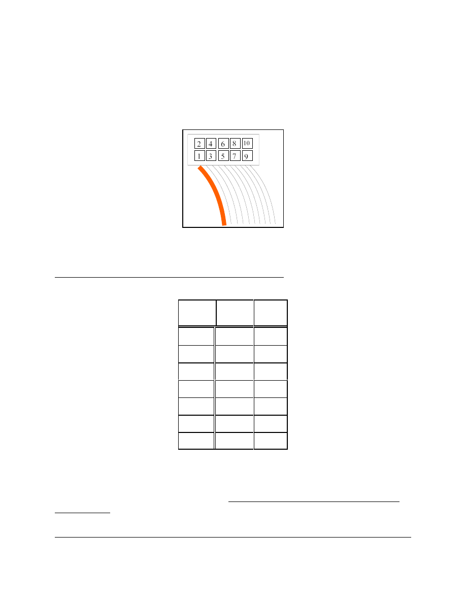
header. Looking at the business end of the header, you should see something like this:
Page 2
05Sep02 L:\Wpdocs\EE 466\Altera Programming.wpd
One side of the ribbon cable has a red wire, while all the others are grey. The red wire (shown
above as a thick line) is tied to pin #1. You will be supplied with an adapter which will allow the
header to be plugged into a breadboard. Remember, the diagram above is looking at the end of
the header. When it’s plugged in, the header will be upside-down from the diagram. Therefore,
the pin locations, when plugged-in, as viewed from the top looking down on the breadboard, will
be:
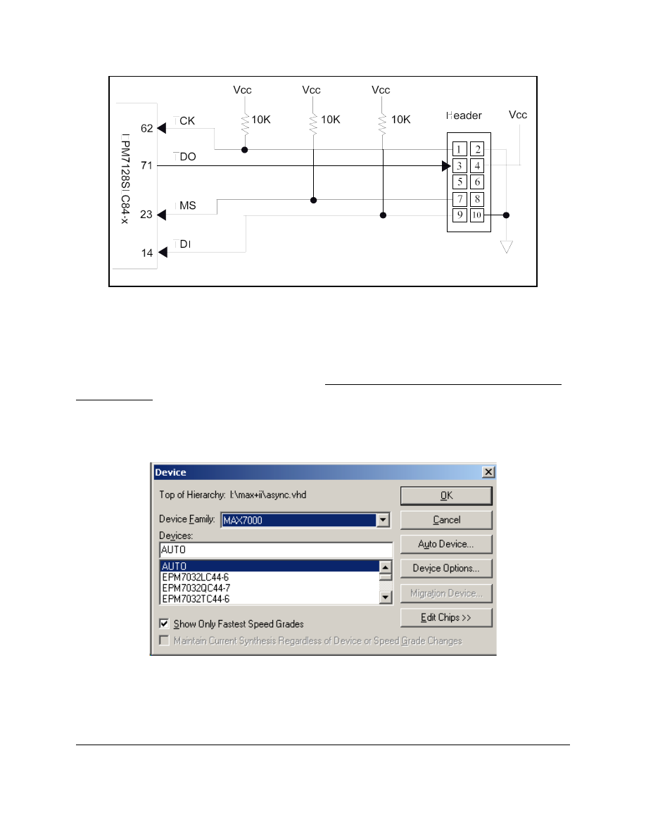
The signals in the header connect to power and the EPLD as shown in the following table. Be
advised this table is specific to the 84 pin PLCC version of the 7128S (EPM7128SLC84-x).
Make all connections to the EPLD while the power is OFF.
Signal
Name
Header
Pin #
EPLD
Pin #
TCK
1
62
GND
2
TDO
3
71
Vcc
4
TMS
5
23
TDI
9
14
GND
10
The three signals which carry information from the computer to the EPLD (TCK, TDI, and
TMS) must be pulled-up to Vcc by 10K resistors. When all is said and done, the circuit should
look like the schematic on the following page. Make all connections to the EPLD while the
power is OFF.
L:\Wpdocs\EE 466\Altera Programming.wpd 06Sep02
Page 3
PROGRAMMING
Before the EPLD can be programmed, the MAX+plus II manager must be configured. Be sure
the ByteBlaster cable is connected at both ends. Make all connections while the power to the
EPLD is OFF.
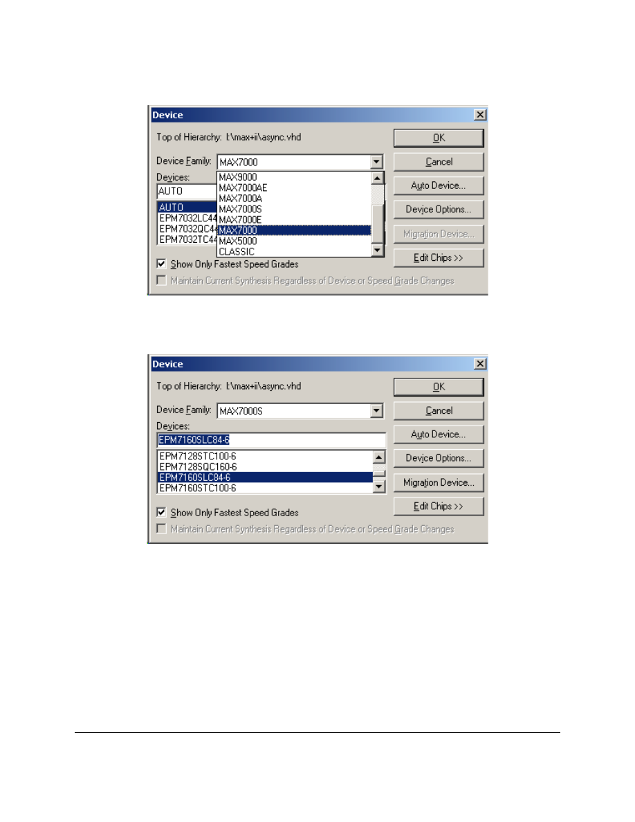
Open the project you wish to program into the EPLD. Pull down the
Assign menu at the top of
the screen and select the
Device option:
Page 4
05Sep02 L:\Wpdocs\EE 466\Altera Programming.wpd
Pull down the
Device Family list in the dialog box:
Select
MAX7000S and then scroll down the devices list in the dialog box until you find
EPM7128SLC84-x, where x is some digit representing the speed of the device:
Select the EPM7128SLC84-x device. If more than one speed grade is shown, select the one with
the largest digit. Now, press the
Device Options button in the dialog box:
L:\Wpdocs\EE 466\Altera Programming.wpd 06Sep02
Page 5
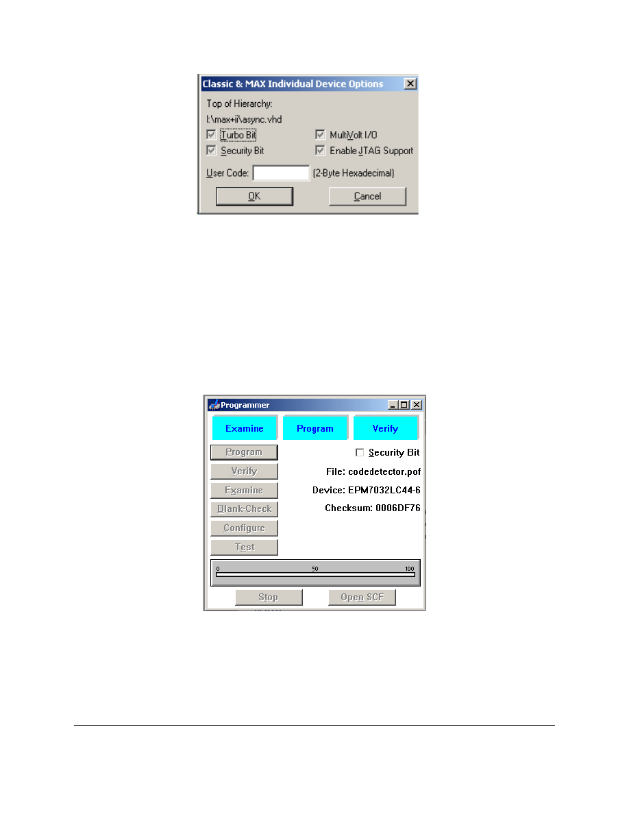
Be sure the
Enable JTAG Support box is checked. Press the OK button to return to the Device
dialog box. You may enter an optional User Code at this point. The User Code will be reported
when the chip is later Examined, see below. If you don’t enter a User Code, the system will
assign one for you. Press the
OK in this box to return to the project window.
Now that your project knows the target device, you should compile and simulate it. Once you’re
satisfied with the results, pull down the
MAX+plus II menu at the top of the screen and select
the
Programmer option:
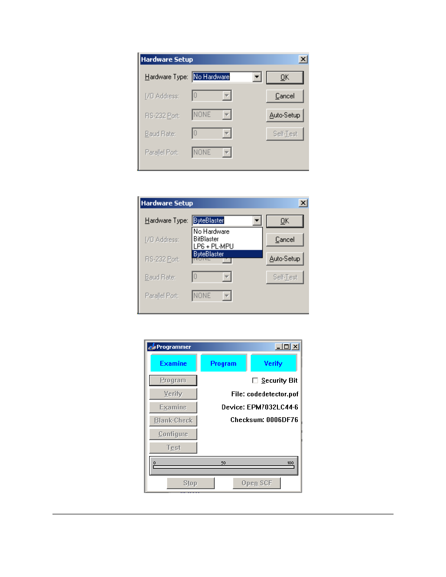
While the Programmer Dialog Box is open, pull down the
Options menu at the top of the screen
and select the
Hardware Setup option:
Page 6
05Sep02 L:\Wpdocs\EE 466\Altera Programming.wpd
Pull down the
Hardware Type list in the dialog box:
and select
ByteBlaster. Press the OK button to return to the Programmer dialog box:
L:\Wpdocs\EE 466\Altera Programming.wpd 06Sep02
Page 7
Turn on the power to the EPLD and associated circuit. Press the
Examine button in the dialog
box. The software will respond with either the contents of the IDCODE register (the User Code
which you may have entered above) or an error message. The error messages are:
ByteBlaster not present The computer can’t find the ByteBlaster. This is usually the result of
an improperly configured parallel port: IRQ, I/O address, or enhanced
setting.
Device not in socket
The ByteBlaster is present, but the software can’t find an EPLD. This
is usually due to not having the JTAG interface enabled, a partially or
improperly seated EPLD (yes- it is possible to force it into the socket
incorrectly), or a bad chip.
If the examination returned a User Code, the chip is ready to program! Just push the
Program
button in the dialog box. Have fun.
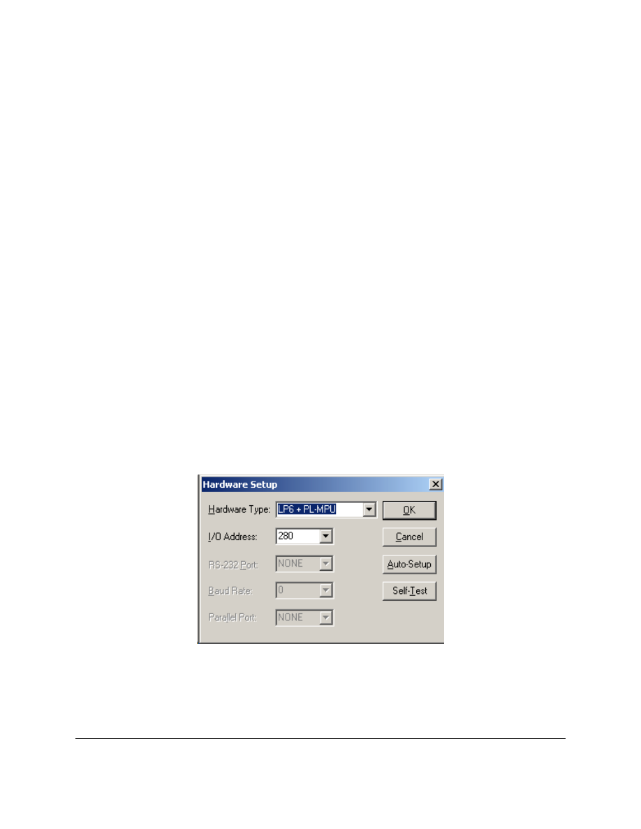
DISABLING THE JTAG INTERFACE
New EPLDs are shipped with the JTAG interface enabled. It can be disabled in the Device
Options dialog (Assign -> Device -> Device Options -> Enable JTAG Support). When the
JTAG interface is disabled there are four more pins available for general I/O assignment. Of
course, the price you pay is having to program the chip out-of-circuit. Out-of-circuit
programming is similar to the procedure described above except for the choice made in the
Hardware Setup dialog (MAX+plus II -> Programmer, Options -> Hardware Setup -> Hardware
Type). Choose
LP6 + PL-MPU instead of ByteBlaster:
Once the JTAG interface is disabled, it can be enabled again only by using the out-of-circuit
programmer.
Wyszukiwarka
Podobne podstrony:
Program The Gateway, Metody pracy
Aktualizacja kart przy użyciu tunera na Linuxie i programu The Last Drakkar
Programing from the Ground Up [PL]
Programming from the Ground Up
Fuck the programme Kees Christiaanse
how to program kess v2 tokens chip
SHSBC377 THE CLASSIFICATION AND GRADATION PROGRAM
CSharp Introduction to C# Programming for the Microsoft NET Platform (Prerelease)
Li Yadav Lin Exploring the role of privacy programs on initial online trust formation
Generics in the Java Programming Language
zedbull transponder clone key programmer transponder chip list
Fuck the programme Kees Christiaanse
Darwin, a Game of Survival of the Fittest among Programs
The Linux Kernel Module Programming Guide
The best Affiliate Program with Life time commision
Chip Off the Old Block
The Problem Of Order In Society, And The Program Of An Analytical Sociology Talcott Parsons,
więcej podobnych podstron