
DATA SHEET
Product specification
Supersedes data of 1995 Apr 28
File under Discrete Semiconductors, SC07
1997 Oct 28
DISCRETE SEMICONDUCTORS
Ideas for design
Small-signal Field-effect
Transistors
1997 Oct 28
2
Philips Semiconductors
Product specification
Small-signal Field-effect Transistors
Ideas for design
JFET CONSTANT-CURRENT SOURCES
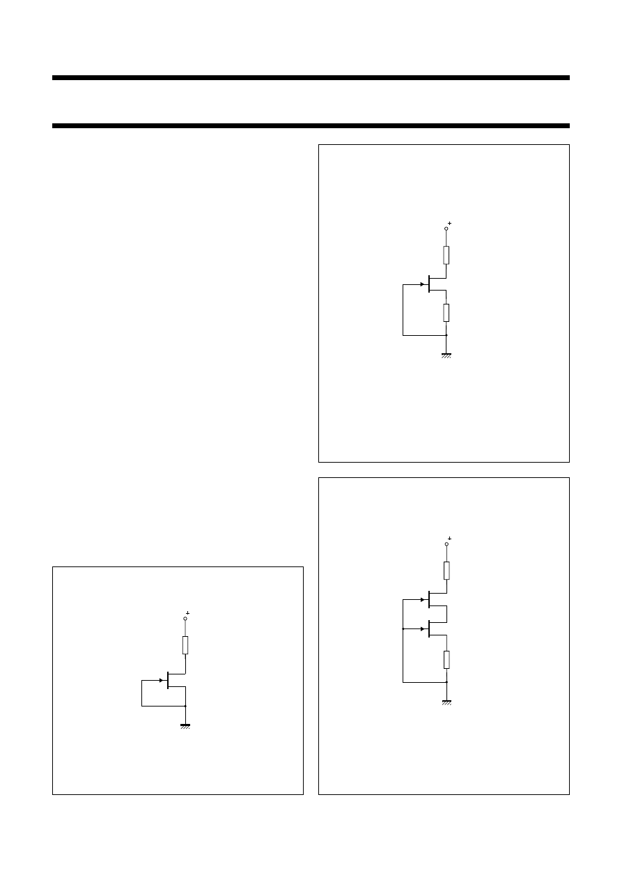
The simplest JFET current source is shown in Fig.1.
The JFET has been selected rather than a MOS-FET
because it does not require gate bias (depletion mode).
The current will be reasonably constant for a V
DS
larger
than several volts. However, because of I
DSS
spread, the
current is unpredictable. This can be seen, for example,
with the 2N5484 which has a specified I
DSS
of 1 to 5 mA.
The circuit is attractive because of its simplicity. (Current
regulator diodes are JFETs with the gate tied to the
source, sorted according to current).
With a small variation this circuit gives an adjustable
current source (see Fig.2). Resistor R back-biases the
gate by V = I
D
×
R, thus reducing I
D
. The value of R can be
calculated from the I
D
/V
G
characteristic for that particular
JFET. This circuit makes it possible to set the current
(must be less than I
DSS
) as well as to make this current
more predictable.
A JFET current source always shows some variation of
output current with output voltage because of its finite
output impedance, even if built with source resistor.
An improvement can be made by using a second JFET to
hold the drain-source voltage of the current source
constant (see Fig.3). The JFET Q2 has a larger I
DSS
and is
connected in series with the current source. It passes the
(constant) drain current from Q1 through to the load, whilst
holding the drain at Q1 at a fixed voltage; namely the
gate-source voltage that makes Q2 operate at the same
current as Q1. Q2 therefore shields Q1 from voltage
swings at its output, and since Q1 is not subject to drain
voltage variations, it provides constant current.
Fig.1 Simple JFET current source.
load
V
MGC451
Fig.2 Adjustable JFET current source.
load
R
V
MGC452
Fig.3
Adjustable JFET current source with high
output impedance.
load
R
Q1
Q2
V
MGC453
1997 Oct 28
3
Philips Semiconductors
Product specification
Small-signal Field-effect Transistors
Ideas for design
JFET SOURCE FOLLOWERS AND AMPLIFIERS
There are normally three major considerations to be taken
into account when designing amplifiers: voltage gain,
distortion and noise, and the importance of each of these
depends on the application. This is also true for the type of
circuit configuration used. There are three basic circuit
configurations for JFETs:
•
Common source configuration (CSC)
•
Common gate configuration (CGC)
•
Common drain configuration (CDC).
The choice of circuit configuration depends on the design
requirements with respect to:
•
Input impedance (high in CSC and CDC)
•
Impedance matching to signal source and load
•
Distortion (lowest in CGC).
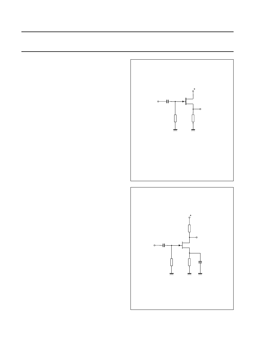
Common-drain amplifiers, or source followers, and
common-source amplifiers are analogous to emitter
followers and common-emitter amplifiers in bipolar
transistors. However, the absence of DC gate current
makes it possible to realize very high input impedances.
Such amplifiers are essential when dealing with the
high-impedance signal sources encountered in
measurement and instrumentation.
It is convenient to use a self-biasing scheme with a single
gate-biasing resistor to ground.
Figure 4 shows a source follower, Fig.5 a common- source
amplifier. The gate-biasing resistor can be quite large
(at least 1 M
Ω
), because the gate leakage current is in the
order of nA.
Matched FETs can be used to construct high input
impedance front-end stages for bipolar differential
amplifiers, op-amps and comparators.
There are many applications in which the signal source
impedance is intrinsically high, e.g. capacitor
microphones, pH probes, charged particle detectors, or
microelectrode signals in biology and medicine. In these
cases a FET input stage is ideal.
Within some circuits there are situations where the
following stage must draw little or no current. Common
examples are analog ‘sample and hold’ and ‘peak
detector’ circuits, in which the level is stored in a capacitor
and will ‘droop’ if the next amplifier draws significant input
current. In all these applications the negligible input
current of a FET is an important feature.
Fig.4 JFET source follower circuit.
out
in
C
Q1
Rg
Rs
V
MGC443
Fig.5 Common-source amplifier circuit.
out
in
C1
Rg
Rs
C2
Q1
Rd
V
MGC442
1997 Oct 28
4
Philips Semiconductors
Product specification
Small-signal Field-effect Transistors
Ideas for design
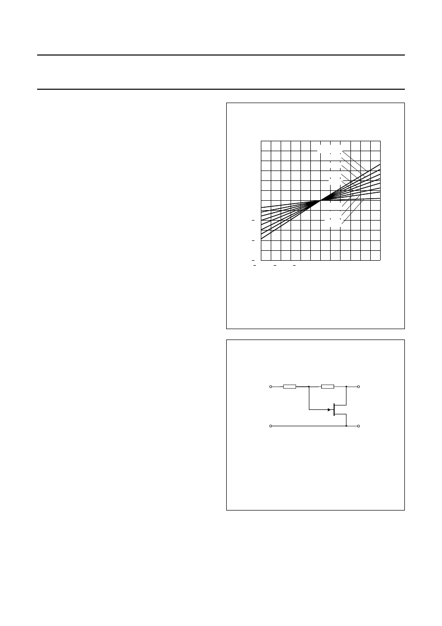
JFET VOLTAGE CONTROLLED RESISTORS
Under certain biasing conditions, the on-resistance of the
JFET is a function of the gate source voltage alone, so that
the JFET will behave as an almost pure ohmic resistor.
Figure 6 shows the output characteristics of a PMBF4416
for relatively small positive and negative values of V
DS
in
the linear or triode region, where V
DS
< V
GS
−
V
GSth
. It can
be seen that all characteristics pass through the origin (no
offset) and are symmetrical and relatively linear. This
means that the JFET can be used as a variable resistance
in voltage controlled attenuators, analog multipliers,
amplitude modulators, bandwidth controlled filters,
automatic gain control circuits, and so on.
The channel resistance in the linear region is the inverse
of the transconductance in the saturated region:
R
DS
= 1/g
m
at a given V
GS
.
In the first quadrant, the boundaries are set by V
GS
= 0 and
V
GD
=
−
V
GSth
, in the third quadrant by V
GS
=
−
V
GSth
and
V
GD
= 0.
In the first quadrant, as V
DS
increases towards
V
DSsat
= V
GS
−
V
GSth
, the value of R
DSon
changes, causing
distortion in voltage-controlled-resistor circuits. The same
thing happens in the third quadrant, as the negative drain
voltage exceeds the negative gate voltage and causes the
gate-channel diode to start conducting.
This signal distortion must be as low as possible, while at
the same time a large signal handling capability is
desirable. The linearity can be improved by means of
feedback from the drain to the gate (see Fig.7).
Now, part of the drain signal is applied to the gate. In the
case of a positive V
DS
signal, this reduces the gate
voltage, increasing the drain current and pushing the bias
line into the more linear part of the operating region.
When V
DS
is negative, V
GS
will go more negative, causing
a reduction in drain current. This reduces the conduction
of the gate channel diode, resulting in a more linear bias
line.
The value of R1 and R2 should be equal, to maintain
symmetry between the first and third quadrants.
Feedback is essential for a reasonably linear
characteristic, and high values of I
DSS
and V
GSth
are
preferred.
Fig.6 Output characteristics; PMBF4416.
0
0.3
0.3
0.2
0.2
3
3
(mA)
ID
VDS (V)
2
2
1
1
0
MGC458
0.1
0.1
VGS = 0V
−
0.5 V
−
1 V
−
1.5 V
−
2 V
−
3 V
−
2.5 V
−
3.5 V
Fig.7 JFET voltage controlled resistor.
RDSon
Vctrl
R2
R1
MGC454
1997 Oct 28
5
Philips Semiconductors
Product specification
Small-signal Field-effect Transistors
Ideas for design
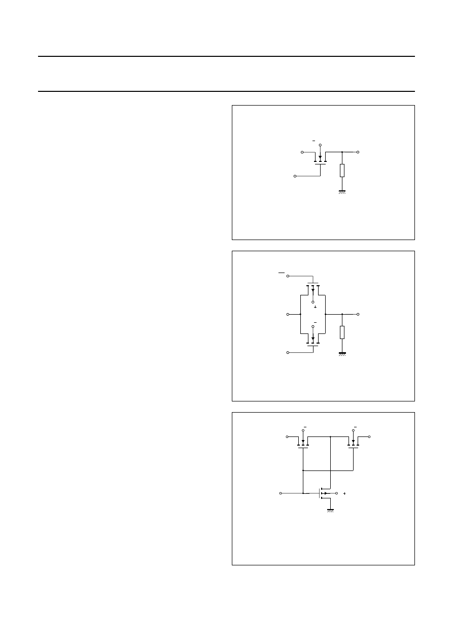
MOS-FET ANALOG SWITCHES
The combination of low on-resistance, extremely high
off-resistance, low leakage current and low capacitance,
makes FETs, particularly lateral MOS-FETs, ideal as
voltage-controlled switching elements for analog signals.
Like mechanical switches, the FET switch is a
bi-directional device; signals can go either way through it.
The circuit as shown in Fig.8 will switch signals in the
−
10
to +10 V range if the gate has been driven from
−
15 V (off)
to +15 V (on); the body (back-gate) should then be tied to
−
15 V.
With any FET switch it is important to provide a load
resistance in the 1 to 100 k
Ω
range in order to reduce
capacitive feed-through of the input signal, that would
otherwise occur during the off-state. If it is necessary to
switch signals that may nearly reach the supply voltages,
the simple N-channel switch shown in Fig.8 will not work,
since the gate is not forward biased at the peak of the
signal swing.
The solution is to use paralleled complementary MOS-FET
switches (Fig.9). In this case the gate-drive is somewhat
more complicated, since the N-channel FET needs to be
positive biased with respect to the back-gate and the
P-channel negative biased. This switch is also
bidirectional; either terminal can be the input.
A useful application of FET analog switches is the
‘multiplexer’, a circuit that allows you to select any of
several inputs, as specified by a control signal. The analog
signal present on the selected input will be passed through
to the output.
Because analog switches are bidirectional, an analog
multiplexer is also a ‘demultiplexer’; a signal can be fed
into the output and will appear on the selected input.
Voltage-controlled analog switches form essential building
blocks for op-amps, integrators, sample-and-hold circuits
and peak detectors.
Another application is in switchable RC low-pass filters.
A multiplexer is used to select one out of a series of
resistors, or independent switches are used to select one
or more resistors in parallel.
As stated before, a load resistor is necessary to reduce
capacitive feed-through (cross-talk).
If a switch that has really low cross-talk performance is
needed, the circuit shown in Fig.10 could be used. When
switches Q1 and Q2 are off, Q3 is on and will prevent any
capacitive feed-through.
Fig.8 MOS-FET analog switch.
15 V
in
control
out
MGC456
Fig.9
Paralleled complementary MOS-FET
switches.
V
V
in
ctrl
ctrl
out
MGC455
Fig.10 MOS-FET analog switch with low cross talk
performance.
V
V
in
Q1
Q2
Q3
ctrl
out
MGC457
V
Wyszukiwarka
Podobne podstrony:
SC07 98 REPLACEMENT 1
SC07 98 GENERAL 1
SC07 MARKING 98 1
(Art 98 a 100)
98 37 WE id 48795 Nieznany (2)
97 98
98
Opara S, Filozofia Współczesne kierunki i problemy, s 98 111
Fringe Tips and Ideas
133 SC DS300 R VW BORA A 98 XX
98 Kwiaty dla dziadka
Instalacja Windows 98
98 o dozorze technicznym id 487 Nieznany (2)
Blanchard European Unemployment The Evolution of Facts and Ideas
PE Nr 05 98
98 91
husserl2, 98
więcej podobnych podstron