
DATA SHEET
Product specification
File under Discrete Semiconductors, SC07
1997 Nov 26
DISCRETE SEMICONDUCTORS
General section
Small-signal Field-effect
Transistors

1997 Nov 26
2
Philips Semiconductors
Product specification
Small-signal Field-effect Transistors
General section
QUALITY
Total Quality Management
Philips Semiconductors is a Quality Company, renowned
for the high quality of our products and service. We keep
alive this tradition by constantly aiming towards one
ultimate standard, that of zero defects. This aim is guided
by our Total Quality Management (TQM) system, the basis
of which is described in the following paragraphs.
Q
UALITY ASSURANCE
Based on ISO 9000 standards, customer standards such
as Ford TQE and IBM MDQ. Our factories are certified to
ISO 9000 by external inspectorates.
P
ARTNERSHIPS WITH CUSTOMERS
PPM co-operations, design-in agreements, ship-to-stock,
just-in-time and self-qualification programmes, and
application support.
P
ARTNERSHIPS WITH SUPPLIERS
Ship-to-stock, statistical process control and ISO 9000
audits.
Q
UALITY IMPROVEMENT PROGRAMME
Continuous process and system improvement, design
improvement, complete use of statistical process control,
realization of our final objective of zero defects, and
logistics improvement by ship-to-stock and just-in-time
agreements.
Advanced quality planning
During the design and development of new products and
processes, quality is built-in by advanced quality planning.
Through failure-mode-and-effect analysis the critical
parameters are detected and measures taken to ensure
good performance on these parameters. The capability of
process steps is also planned in this phase.
Product conformance
The assurance of product conformance is an integral part
of our quality assurance (QA) practice. This is achieved by:
•
Incoming material management through partnerships
with suppliers.
•
In-line quality assurance to monitor process
reproducibility during manufacture and initiate any
necessary corrective action. Critical process steps are
100% under statistical process control.
•
Acceptance tests on finished products to verify
conformance with the device specification. The test
results are used for quality feedback and corrective
actions. The inspection and test requirements are
detailed in the general quality specifications.
•
Periodic inspections to monitor and measure the
conformance of products.
Product reliability
With the increasing complexity of Original Equipment
Manufacturer (OEM) equipment, component reliability
must be extremely high. Our research laboratories and
development departments study the failure mechanisms of
semiconductors. Their studies result in design rules and
process optimization for the highest built-in product
reliability. Highly accelerated tests are applied to the
products reliability evaluation. Rejects from reliability tests
and from customer complaints are submitted to failure
analysis, to result in corrective action.
Customer responses
Our quality improvement depends on joint action with our
customer. We need our customer’s inputs and we invite
constructive comments on all aspects of our performance.
Please contact our local sales representative.
Recognition
The high quality of our products and services is
demonstrated by many Quality Awards granted by major
customers and international organizations.
PRO ELECTRON TYPE NUMBERING SYSTEM
Basic type number
This type designation code applies to discrete
semiconductor devices (not integrated circuits), multiples
of such devices, semiconductor chips and Darlington
transistors.
F
IRST LETTER
The first letter gives information about the material for the
active part of the device.
A
germanium or other material with a band gap of
0.6 to 1 eV
B
silicon or other material with a band gap of 1 to 1.3 eV
C
gallium arsenide (GaAs) or other material with a band
gap of 1.3 eV or more
R
compound materials, e.g. cadmium sulphide

1997 Nov 26
3
Philips Semiconductors
Product specification
Small-signal Field-effect Transistors
General section
S
ECOND LETTER
The second letter indicates the function for which the
device is primarily designed. The same letter can be used
for multi-chip devices with similar elements.
In the following list low power types are defined by
R
th j-mb
> 15 K/W and power types by R
th j-mb
≤
15 K/W.
A
diode; signal, low power
B
diode; variable capacitance
C
transistor; low power, audio frequency
D
transistor; power, audio frequency
E
diode; tunnel
F
transistor; low power, high frequency
G
multiple of dissimilar devices/miscellaneous devices;
e.g. oscillators. Also with special third letter; see under
Section “Serial number”.
H
diode; magnetic sensitive
L
transistor; power, high frequency
N
photocoupler
P
radiation detector; e.g. high sensitivity
photo-transistor; with special third letter
Q
radiation generator; e.g. LED, laser; with special third
letter
R
control or switching device; e.g. thyristor, low power;
with special third letter
S
transistor; low power, switching
T
control or switching device; e.g. thyristor, low power;
with special third letter
U
transistor; power, switching
W surface acoustic wave device
X
diode; multiplier, e.g. varactor, step recovery
Y
diode; rectifying, booster
Z
diode; voltage reference or regulator, transient
suppressor diode; with special third letter.
S
ERIAL NUMBER
The number comprises three figures running from
100 to 999 for devices primarily intended for consumer
equipment, or one letter (Z, Y, X, etc.) and two figures
running from 10 to 99 for devices primarily intended for
industrial or professional equipment.
(1)
(1) When the supply of these serial numbers is exhausted, the
serial number may be expanded to three figures for industrial
types and four figures for consumer types.
Version letter
A letter may be added to the basic type number to indicate
minor electrical or mechanical variants of the basic type.
RATING SYSTEMS
The rating systems described are those recommended by
the IEC in its publication number 134.
Definitions of terms used
E
LECTRONIC DEVICE
An electronic tube or valve, transistor or other
semiconductor device. This definition excludes inductors,
capacitors, resistors and similar components.
C
HARACTERISTIC
A characteristic is an inherent and measurable property of
a device. Such a property may be electrical, mechanical,
thermal, hydraulic, electro-magnetic or nuclear, and can
be expressed as a value for stated or recognized
conditions. A characteristic may also be a set of related
values, usually shown in graphical form.
B
OGEY ELECTRONIC DEVICE
An electronic device whose characteristics have the
published nominal values for the type. A bogey electronic
device for any particular application can be obtained by
considering only those characteristics that are directly
related to the application.
R
ATING
A value that establishes either a limiting capability or a
limiting condition for an electronic device. It is determined
for specified values of environment and operation, and
may be stated in any suitable terms. Limiting conditions
may be either maxima or minima.
R
ATING SYSTEM
The set of principles upon which ratings are established
and which determine their interpretation. The rating
system indicates the division of responsibility between the
device manufacturer and the circuit designer, with the
object of ensuring that the working conditions do not
exceed the ratings.
Absolute maximum rating system
Absolute maximum ratings are limiting values of operating
and environmental conditions applicable to any electronic

1997 Nov 26
4
Philips Semiconductors
Product specification
Small-signal Field-effect Transistors
General section
device of a specified type, as defined by its published data,
which should not be exceeded under the worst probable
conditions.
These values are chosen by the device manufacturer to
provide acceptable serviceability of the device, taking no
responsibility for equipment variations, environmental
variations, and the effects of changes in operating
conditions due to variations in the characteristics of the
device under consideration and of all other electronic
devices in the equipment.
The equipment manufacturer should design so that,
initially and throughout the life of the device, no absolute
maximum value for the intended service is exceeded with
any device, under the worst probable operating conditions
with respect to supply voltage variation, equipment
component variation, equipment control adjustment, load
variations, signal variation, environmental conditions, and
variations in characteristics of the device under
consideration and of all other electronic devices in the
equipment.
Design maximum rating system
Design maximum ratings are limiting values of operating
and environmental conditions applicable to a bogey
electronic device of a specified type as defined by its
published data, and should not be exceeded under the
worst probable conditions.
These values are chosen by the device manufacturer to
provide acceptable serviceability of the device, taking
responsibility for the effects of changes in operating
conditions due to variations in the characteristics of the
electronic device under consideration.
The equipment manufacturer should design so that,
initially and throughout the life of the device, no design
maximum value for the intended service is exceeded with
a bogey electronic device, under the worst probable
operating conditions with respect to supply voltage
variation, equipment component variation, variation in
characteristics of all other devices in the equipment,
equipment control adjustment, load variation, signal
variation and environmental conditions.
Design centre rating system
Design centre ratings are limiting values of operating and
environmental conditions applicable to a bogey electronic
device of a specified type as defined by its published data,
and should not be exceeded under normal conditions.
These values are chosen by the device manufacturer to
provide acceptable serviceability of the device in average
applications, taking responsibility for normal changes in
operating conditions due to rated supply voltage variation,
equipment component variation, equipment control
adjustment, load variation, signal variation, environmental
conditions, and variations in the characteristics of all
electronic devices.
The equipment manufacturer should design so that,
initially, no design centre value for the intended service is
exceeded with a bogey electronic device in equipment
operating at the stated normal supply voltage.
LETTER SYMBOLS
The letter symbols for transistors detailed in this section
are based on IEC publication number 148.
Basic letters
In the representation of currents, voltages and powers,
lower-case letter symbols are used to indicate all
instantaneous values that vary with time. All other values
are represented by upper-case letters.
Electrical parameters
(1)
of external circuits and of circuits
in which the device forms only a part are represented by
upper-case letters. Lower-case letters are used for the
representation of electrical parameters inherent in the
device. Inductances and capacitances are always
represented by upper-case letters.
The following is a list of basic letter symbols used with
semiconductor devices:
B, b susceptance (imaginary part of an admittance)
C
capacitance
G, g conductance (real part of an admittance)
H, h hybrid parameter
I, i
current
L
inductance
P, p
power
R, r
resistance (real part of an impedance)
V, v
voltage
X, x reactance (imaginary part of an impedance)
Y, y
admittance
Z, z
impedance
(1) For the purpose of this publication, the term ‘electrical
parameters’ applies to four-pole matrix parameters, elements
of electrical equivalent circuits, electrical impedances and
admittances, inductances and capacitances.

1997 Nov 26
5
Philips Semiconductors
Product specification
Small-signal Field-effect Transistors
General section
Subscripts
Upper-case subscripts are used for the indication of:
•
continuous (DC) values (without signal), e.g. I
D
•
instantaneous total values, e.g. i
D
•
average total values, e.g. I
D(AV)
•
peak total values, e.g. I
DM
•
root-mean-square total values, e.g. I
D(RMS)
.
Lower-case subscripts are used for the indication of values
applying to the varying component alone:
•
instantaneous values, e.g. i
b
•
root-mean-square values, e.g. I
d(rms)
•
peak values, e.g. I
dm
•
average values, e.g. I
d(av)
.
The following is a list of subscripts used with basic letter
symbols for semiconductor devices:
A, a
anode
amb
ambient
(AV), (av)
average value
B, b
base
(BO)
breakover
(BR)
breakdown
case
case
C, c
collector
C
controllable
D, d
drain
E, e
emitter
F, f
fall, forward (or forward transfer)
G, g
gate
H
holding
h
heatsink
I, i
input
j-a
junction to ambient
j-mb
junction to mounting base
K, k
cathode
L
load
M, m
peak value
(min)
minimum
(max)
maximum
mb
mounting base
O, o
as third subscript: the terminal not
mentioned is open-circuit
Applications and examples
T
RANSISTOR CURRENTS
The first subscript indicates the terminal carrying the
current (conventional current flow from the external circuit
into the terminal is positive).
Examples: I
D
, i
D
, i
d
, I
dm
.
T
RANSISTOR VOLTAGES
A voltage is indicated by the first two subscripts: the first
identifies the terminal at which the voltage is measured
and the second the reference terminal or the circuit node.
The second subscript may be omitted when there is no
possibility of confusion.
Examples: V
GS
, v
GS
, v
gs
, V
gsm
.
S
UPPLY VOLTAGES OR CURRENTS
Supply voltages or supply currents are indicated by
repeating the appropriate terminal subscript.
Examples: V
DD
, I
SS
.
(OV)
overload
P, p
pulse
Q, q
turn-off
R, r
as first subscript: reverse (or reverse
transfer), rise. As second subscript:
repetitive, recovery. As third subscript:
with a specified resistance between the
terminal not mentioned and the
reference terminal
(RMS), (rms)
root-mean-square value
S, s
as first subscript: series, source,
storage, stray, switching. As second
subscript: surge (non-repetitive). As third
subscript: short circuit between the
terminal not mentioned and the
reference terminal
stg
storage
th
thermal
TO
threshold
tot
total
W
working
X, x
specified circuit
Z, z
reference or regulator (zener)
1
input (four-pole matrix)
2
output (four-pole matrix).

1997 Nov 26
6
Philips Semiconductors
Product specification
Small-signal Field-effect Transistors
General section
A reference terminal is indicated by a third subscript.
Example: V
DDS
.
D
EVICES WITH MORE THAN ONE TERMINAL OF THE SAME KIND
If a device has more than one terminal of the same kind,
the subscript is formed by the appropriate letter for the
terminal, followed by a number. Hyphens may be used to
avoid confusion in multiple subscripts.
Examples:
M
ULTIPLE DEVICES
For multiple unit devices, the subscripts are modified by a
number preceding the letter subscript. Hyphens may be
used to avoid confusion in multiple subscripts.
Examples:
E
LECTRICAL PARAMETERS
The upper-case variant of a subscript is used for the
designation of static (DC) values.
Examples:
The static value is the slope of the line from the origin to
the operating point on the appropriate characteristic curve,
i.e. the quotient of the appropriate electrical quantities at
the operating point.
I
G2
continuous (DC) current flowing into the
second gate terminal
V
G2-S
continuous (DC) voltage between the
terminals of second gate and source.
I
2D
continuous (DC) current flowing into the drain
terminal of the second unit
V
1D-2D
continuous (DC) voltage between the drain
terminals of the first and second units.
g
FS
static value of forward transconductance in
common-source configuration (DC current
gain)
R
DS
DC value of the drain-source resistance.
The lower-case variant of a subscript is used for the
designation of small-signal values.
Examples:
If more than one subscript is used, subscripts for which a
choice of style is allowed, the subscripts chosen are all
upper-case or all lower-case.
Examples: h
FE
, y
RE
, h
fe
, g
FS
.
F
OUR
-
POLE MATRIX PARAMETERS
The first letter subscript (or double numeric subscript)
indicates input, output, forward transfer or reverse
transfer.
Examples: h
i
(or h
11
), h
o
(or h
22
), h
f
(or h
21
), h
r
(or h
12
).
A further subscript is used for the identification of the circuit
configuration. When no confusion is possible, this further
subscript may be omitted.
Examples: h
fe
(or h
21e
), h
FE
(or h
21E
).
D
ISTINCTION BETWEEN REAL AND IMAGINARY PARTS
If it is necessary to distinguish between real and imaginary
parts of electrical parameters, no additional subscripts are
used. If basic symbols for the real and imaginary parts
exist, these may be used.
Examples: Z
i
= R
i
+ jX
i
, y
fe
= g
fe
+ jb
fe
.
If such symbols do not exist or are not suitable, the
notation shown in the following examples is used.
Examples:
Re (h
ib
) etc. for the real part of h
ib
.
Im (h
ib
) etc. for the imaginary part of h
ib
.
g
fs
small-signal value of the short-circuit
forward transconductance in
common-source configuration
Z
i
= R
i
+ jX
i
small-signal value of the input
impedance.
1997 Nov 26
7
Philips Semiconductors
Product specification
Small-signal Field-effect Transistors
General section
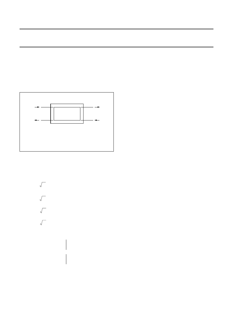
S-PARAMETER DEFINITIONS
The S-parameter symbols in this section are based on IEC
publication 747-7.
S-parameters (return losses or reflection coefficients) of a
module can be defined as the S
11
and the S
22
of a two-port
network (see Fig.1).
(1)
(2)
where:
(3)
(4)
From (1) and (2) formulae for the return losses can be
derived:
(5)
(6)
In (5), a
2
= 0 means output port terminated with Z
o
(derived from formula (4)).
In (6), a
1
= 0 means input port terminated with Z
o
(derived from formula (3)).
Fig.1
Two-port network with reflection coefficients
S11 and S22.
D.U.T.
S11
S 22
a 1
b 1
b 2
a 2
MLB335
b
1
S
11
a
1
S
12
a
2
⋅
+
⋅
=
b
2
S
21
a
1
S
22
a
2
⋅
+
⋅
=
a
1
1
2
Z
o
⋅
------------------
V
1
Z
o
i
1
⋅
+
(
)
⋅
signal into port 1
=
=
a
2
1
2
Z
o
⋅
------------------
V
2
Z
o
i
2
⋅
+
(
)
⋅
signal into port 2
=
=
b
1
1
2
Z
o
⋅
------------------
V
1
Z
o
i
1
⋅
+
(
)
⋅
signal out port 1
=
=
b
2
1
2
Z
o
⋅
------------------
V
1
Z
o
i
2
⋅
+
(
)
⋅
signal out port 2
=
=
S
11
b
1
a
1
------ a
2
0
=
=
S
22
b
2
a
2
------ a
1
0
=
=
Measurement
The return losses are measured with a network analyzer
after calibration, where the influence of the test jig is
eliminated. The necessary termination of the other port
with Z
o
is done automatically by the network analyzer.
The network analyser must have a directivity of at least
40 dB to obtain an accuracy of 0.5 dB when measuring
return loss figures of 20 dB. A full two-port correction
method can be used to improve the accuracy.
TAPE AND REEL PACKING
Tape and reel packing meets the feed requirements of
automatic pick and place equipment (packing conforms to
IEC publication 286-2 and 286-3). Additionally, the tape is
an ideal shipping container.
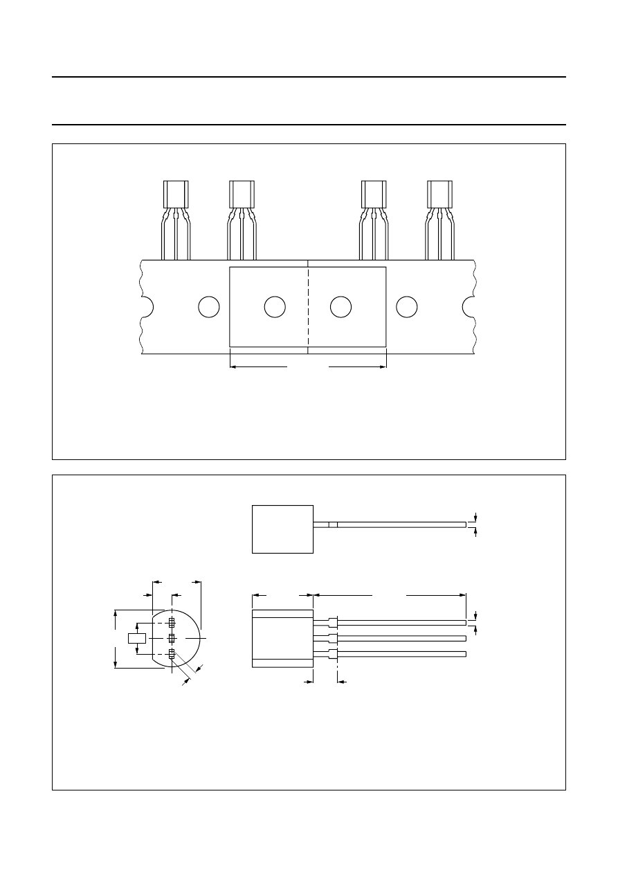
Packing (TO-92 leaded types)
The transistors are supplied on tape in boxes (ammopack)
or on reels. The number per reel and per ammopack is
2000. The ammopack has 80 layers of 25 transistors
each. Each layer contains 25 transistors, plus one empty
position in order to fold the layer correctly. The ammopack
is accessible from both sides, enabling the user to choose
between ‘normal’ (see Fig.3) and ‘reverse’ tape. ‘Normal’
is indicated by a plus sign (+) on the ammopack and
‘reverse’ by a minus sign (
−
). In the European version, the
leading pin is the source.
1997 Nov 26
8
Philips Semiconductors
Product specification
Small-signal Field-effect Transistors
General section
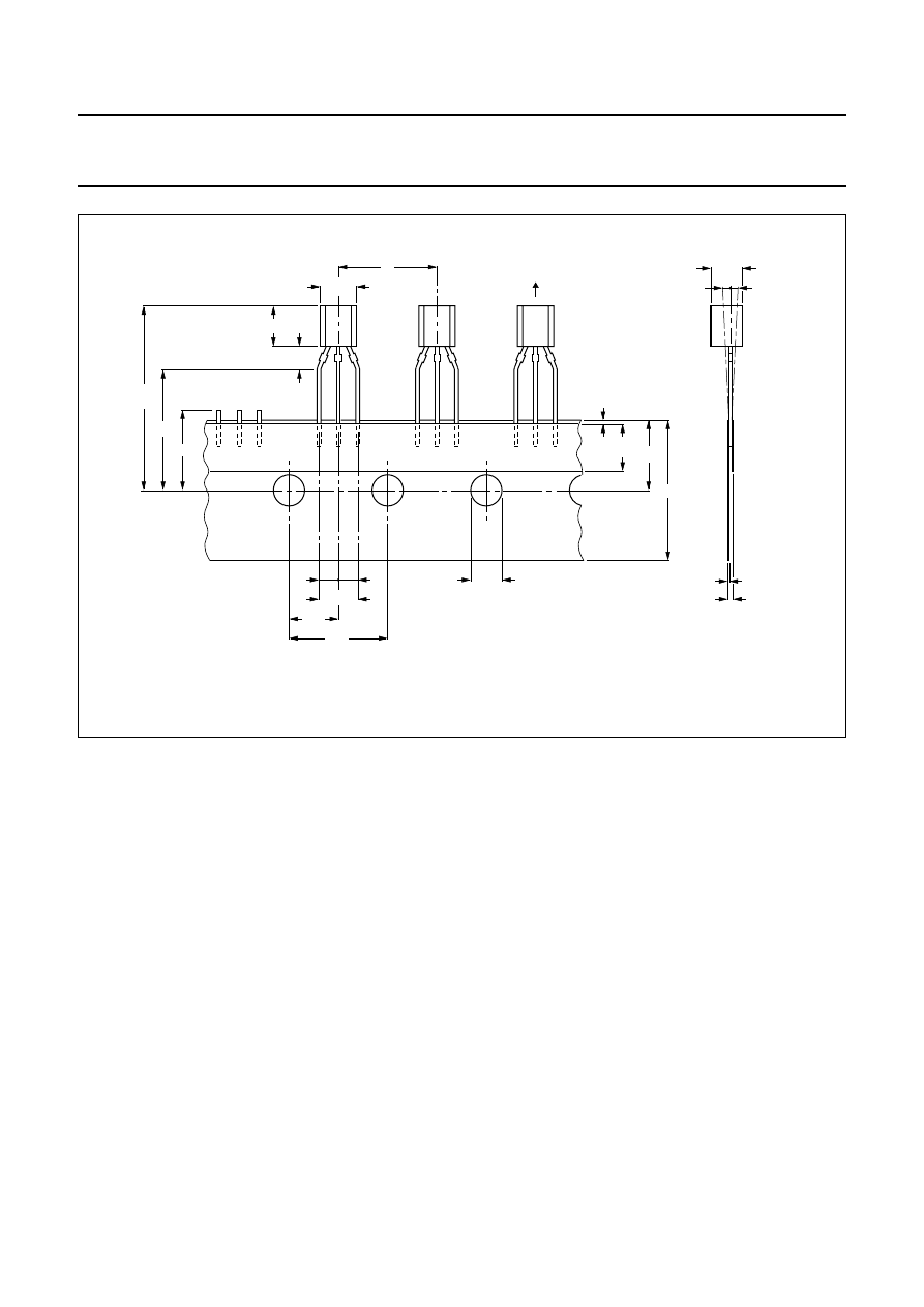
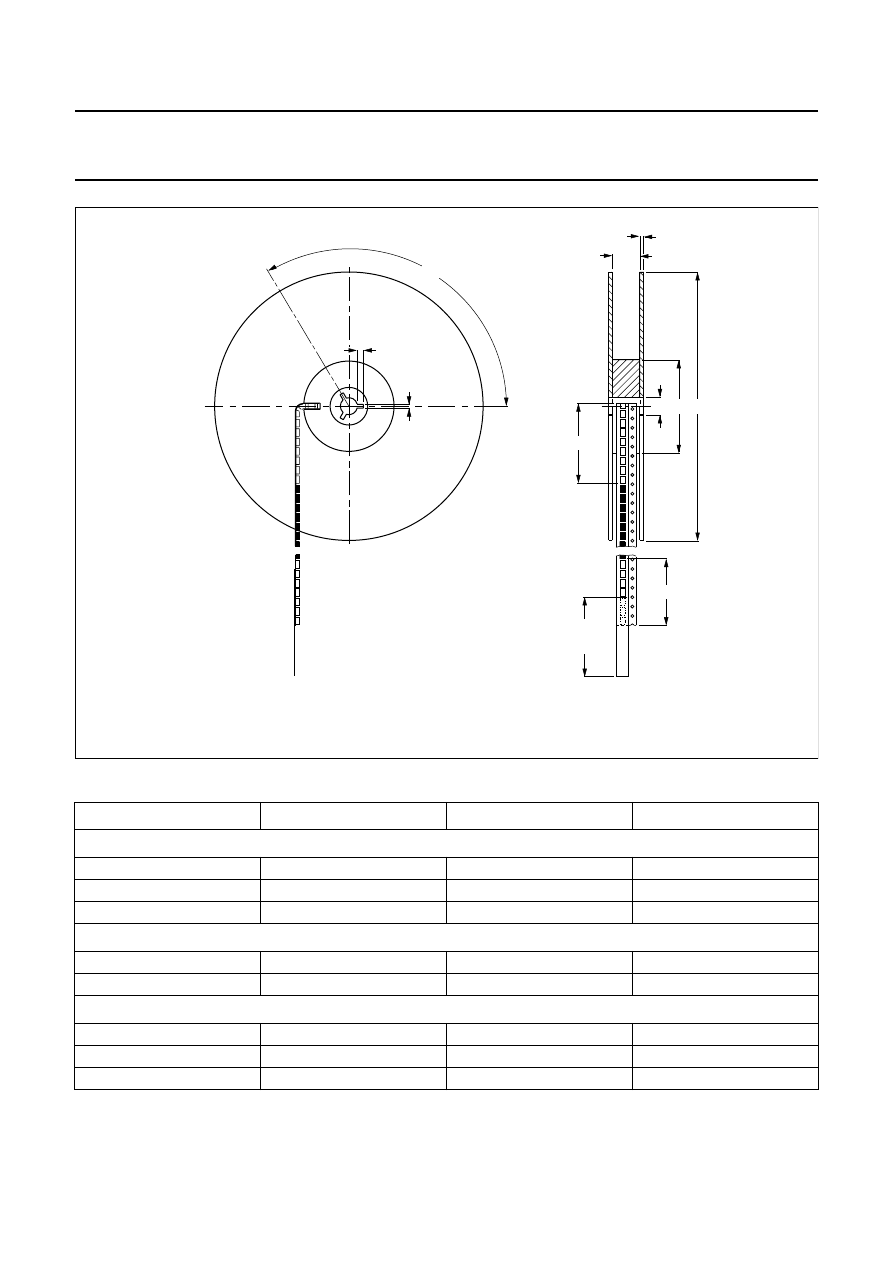
Fig.2 TO-92 transistors on tape.
handbook, full pagewidth
MEA940
(p)
A1
H2
W1
t1
W0
D0
F1
F2
P2
P0
W2
H1
H0
P
A
L
F
W
t
∆
h
∆
h
T
1997 Nov 26
9
Philips Semiconductors
Product specification
Small-signal Field-effect Transistors
General section
Table 1
Tape specification (TO-92 leaded types)
Note
1. Measured over 20 devices.
SYMBOL
DIMENSION
SPECIFICATIONS
REMARKS
MIN.
NOM.
MAX.
TOL.
UNIT
A
1
body width
4
−
4.8
−
mm
A
body height
4.8
−
5.2
−
mm
T
body thickness
3.5
−
3.9
−
mm
P
pitch of component
−
12.7
−
±
1
mm
P
0
feed hole pitch
−
12.7
−
±
0.3
mm
cumulative pitch error
−
−
−
±
0.1
note 1
P
2
feed hole centre to component
centre
−
6.35
−
±
0.4
mm
to be measured at bottom
of clinch
F
distance between outer leads
−
5.08
−
+0.6/
−
0.2
mm
∆
h
component alignment
−
0
1
−
mm
at top of body
W
tape width
−
18
−
±
0.5
mm
W
0
hold-down tape width
−
6
−
±
0.2
mm
W
1
hole position
−
9
−
+0.7/
−
0.5
mm
W
2
hold-down tape position
−
0.5
−
±
0.2
mm
H
0
lead wire clinch height
−
16.5
−
±
0.5
mm
H
1
component height
−
−
23.25
−
mm
L
length of snipped leads
−
−
11
−
mm
D
0
feed hole diameter
−
4
−
±
0.2
mm
t
total tape thickness
−
−
1.2
−
mm
t
1
= 0.3 to 0.6
F
1
, F
2
lead-to-lead distance
−
−
−
+0.4/
−
0.2
mm
H
2
clinch height
−
−
−
−
mm
(p)
pull-out force
6
−
−
−
N
Dropouts
A maximum of 0.5% of the specified number of transistors
in each packing may be missing. Up to 3 consecutive
components may be missing provided the gap is followed
by 6 consecutive components.
Tape splicing
Splice the carrier tape on the back and/or front so that the
feed hole pitch (P
0
) is maintained (see Figs 2 and 4).
1997 Nov 26
10
Philips Semiconductors
Product specification
Small-signal Field-effect Transistors
General section
Fig.3 Dimensions of reel and box.
Dimensions in mm.
handbook, full pagewidth
(1)
∅
380
min
∅
15
min
55 max
55 max
350
max
(1)
A
A
MEA473
direction of unreeling
A - A
(1)
packing label
1997 Nov 26
11
Philips Semiconductors
Product specification
Small-signal Field-effect Transistors
General section
Fig.4 Joining tape with splicing patch.
dbook, full pagewidth
MEA941
30 mm min
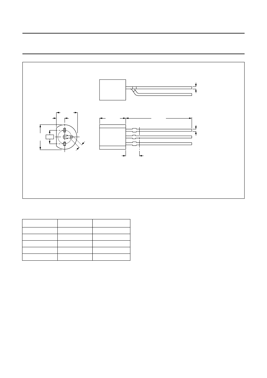
Fig.5 TO-92 with straight leads.
Dimensions in mm.
(1) Terminal dimensions within this zone are uncontrolled to allow for flow of plastic and terminal irregularities.
ndbook, full pagewidth
MBC014 - 1
2.54
4.8
max
4.2 max
1.7
1.4
0.66
0.56
1
2
3
5.2 max
12.7 min
2.0 max
(1)
0.48
0.40
0.40
min
1997 Nov 26
12
Philips Semiconductors
Product specification
Small-signal Field-effect Transistors
General section
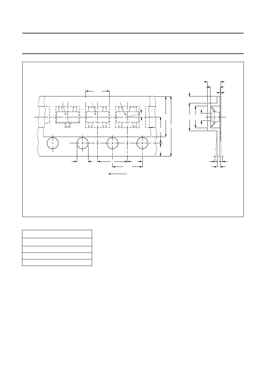
Fig.6 TO-92 with delta pinning.
Dimensions in mm.
(1) Terminal dimensions within this zone are uncontrolled to allow for flow of plastic and terminal irregularities.
ok, full pagewidth
MBC015 - 1
2.54
4.8
max
4.2 max
0.66
0.56
1
2
3
5.2 max
12.7 min
2.5 max
(1)
0.48
0.40
0.40
min
1.7
1.4
Packing SMD types
Table 2
Packing quantities per reel (SMD types)
PACKAGE
180 mm REEL
330 mm REEL
SOT23
3000
10000
SOT143
3000
10000
SOT143R
3000
10000
SOT343
3000
10000
SOT343R
3000
10000
1997 Nov 26
13
Philips Semiconductors
Product specification
Small-signal Field-effect Transistors
General section
Table 3
Carrier tape widths for packages
CARRIER TAPE
8 mm
SOT23
SOT143(R)
SOT343(R)
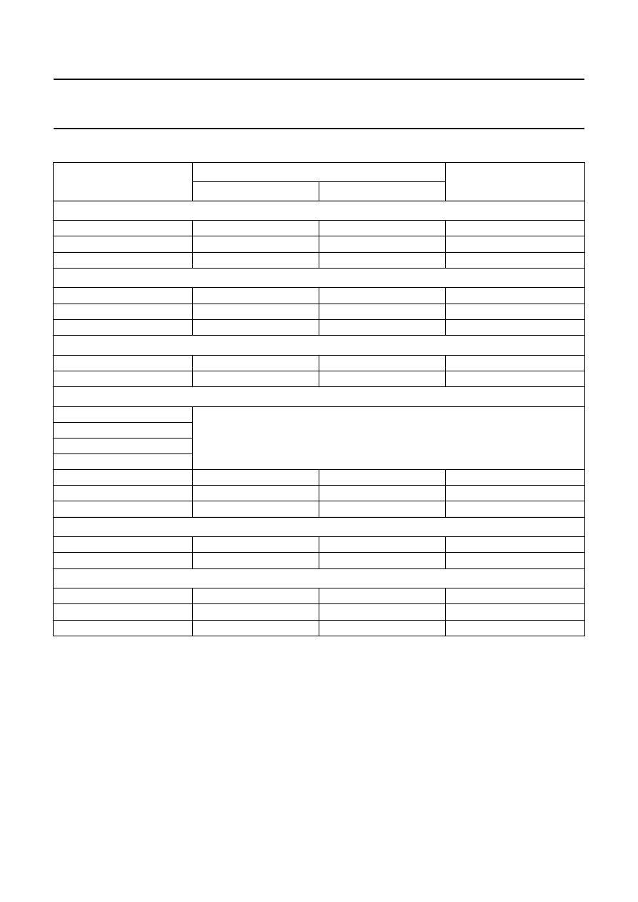
Fig.7 Specification for 8 mm tape (SOT23, SOT143, SOT143R, SOT343 and SOT343R).
For dimensions see Table 4.
(1) Tolerance over any 10 pitches:
±
0.2 mm.
andbook, full pagewidth
MBE547 - 1
E
P
D 0
P0
P2
F
W1
W
direction of unreeling
,,,
,,,
,,,
,,,
,,,
,,,
,
,
,
,
,
T
δ
δ
B1 B0 D1
K
K 0
SOT143R/343R
SOT143/343
A 0
θ
T1
SOT23
G
(1)
1997 Nov 26
14
Philips Semiconductors
Product specification
Small-signal Field-effect Transistors
General section
Table 4
SMD packages: tape dimensions (in mm)
Notes
1. Tolerance over any 10 pitches
±
0.2 mm.
2. The cover tape shall not overlap the tape or sprocket holes.
DIMENSION
(Figs 7 to 10)
CARRIER TAPE
TOLERANCE
8 mm
12 mm
Overall dimensions
W
8.0
12.0
±
0.2
K
<1.5
<2.4
−
G
>0.75
>0.75
−
Sprocket holes; note 1
D
0
1.5
1.5
+0.1/
−
0
E
1.75
1.75
±
0.1
P
0
4.0
4.0
±
0.1
Relative placement compartment
P
2
2.0
2.0
±
0.1
F
3.5
5.5
±
0.05
Compartment
A
0
Compartment dimensions depend on package size. Maximum clearance between
device and compartment is 0.3 mm; the minimum clearance ensures that the device
is not totally restrained within the compartment.
B
0
B
1
K
0
D
1
>1.0
>1.5
−
P
4.0
8.0
±
0.1
θ
<15
°
<15
°
−
Cover tape; note 2
W
1
<5.4
<9.5
−
T
1
<0.1
<0.1
−
Carrier tape
W
8.0
12.0
±
0.2
T
<0.2
<0.2
−
δ
<0.3
<0.3
−
1997 Nov 26
15
Philips Semiconductors
Product specification
Small-signal Field-effect Transistors
General section
Table 5
Reel dimensions (in mm)
Note
1. Large reel diameter depends on individual package (286 or 350).
DIMENSION (see Fig.8)
8 mm TAPE
12 mm TAPE
TOLERANCE
Flange
A
180
(1)
−
286 or 330
180 or 330
±
0.5
t
1.5
1.5
+0.5/
−
0.1
W
8.4
12.4
18.0+0.2
Hub
B
62
62
±
1.5
C
12.75
12.75
+0.15/
−
0.2
Key slot
E
2
2
±
0.2
U
4
4
±
0.5
O
120
°
120
°
−
Fig.8 Reel specification.
For dimensions see Table 5.
handbook, full pagewidth
MEA942
O
E
U
leader
fixing
tape
trailer
C
B
A
W
t

1997 Nov 26
16
Philips Semiconductors
Product specification
Small-signal Field-effect Transistors
General section
MOUNTING AND SOLDERING
Mounting methods
There are two basic forms of electronic component
construction, those with leads for through-hole mounting
and microminiature types for surface mounting (SMD).
Through-hole mounting gives a very rugged construction
and uses well established soldering methods. Surface
mounting has the advantages of high packing density plus
high-speed automated assembly. Surface mounting
techniques are complex and this chapter gives only a
simplified overview of the subject.
Although many electronic components are available as
surface mounting types, some are not and this often leads
to the use of through-hole as well as surface mounting
components on one substrate (a mixed print). The mix of
components affects the soldering methods that can be
applied. A substrate having SMDs mounted on one or both
sides but no through-hole components is likely to be
suitable for reflow or wave soldering. A double sided mixed
print that has through-hole components and some SMDs
on one side and densely packed SMDs on the other
normally undergoes a sequential combination of reflow
and wave soldering. When the mixed print has only
through-hole components on one side and all SMDs on the
other, wave soldering is usually applied.
Reflow soldering
S
OLDER PASTE
Most reflow soldering techniques utilize a paste that is a
mixture of flux and solder. The solder paste is applied to
the substrate before the components are placed. It is of
sufficient viscosity to hold the components in place and,
therefore, an application of adhesive is not required.
Drying of the solder paste by preheating increases the
viscosity and prevents any tendency for the components to
become displaced during the soldering process.
Preheating also minimizes thermal shock and drives off
flux solvents.
Screen printing
This is the best high-volume production method of solder
paste application. An emulsion-coated, fine mesh screen
with apertures etched in the emulsion to coincide with the
surfaces to be soldered is placed over the substrate. A
squeegee is passed across the screen to force solder
paste through the apertures and on to the substrate. The
layer thickness of screened solder paste is usually
between 150 and 200
µ
m.
Stencilling
In this method a stencil with etched holes to pass the paste
is used. The thickness of the stencil determines the
amount of amount of solder paste that is deposited on the
substrate. This method is also suited to high-volume work.
Dispensing
A computer-controlled pressure syringe dispenses small
doses of paste to where it is required. This method is
mainly suitable for small production runs and laboratory
use.
Pin transfer
A pin picks up a droplet of solder paste from a reservoir
and transfers it to the surface of the substrate or
component. A multi-pin arrangement with pins positioned
to match the substrate is possible and this speeds up the
process time.
R
EFLOW TECHNIQUES
Thermal conduction
The prepared substrates are carried on a conveyor belt,
first through a preheating stage and then through a
soldering stage. Heat is transferred to the substrate by
conduction through the belt. Figure 9 shows a theoretical
time/temperature relationship for thermal conduction
reflow soldering. This method is particularly suited to thick
film substrates and is often combined with infrared
heating.

1997 Nov 26
17
Philips Semiconductors
Product specification
Small-signal Field-effect Transistors
General section
Infrared
An infrared oven has several heating elements giving a
broad spectrum of infrared radiation, normally above and
below a closed loop belt system. There are separate zones
for preheating, soldering and cooling. Dwell time in the
soldering zone is kept as short as possible to prevent
damage to components and substrate. A typical heating
profile is shown in Fig.10. This reflow method is often
applied in double-sided prints.
Vapour phase
A substrate is immersed in the vapours of a suitable boiling
liquid. The vapours transfer latent heat of condensation to
the substrate and solder reflow takes place. Temperature
is controlled precisely by the boiling point of the liquid at a
given pressure. Some systems employ two vapour zones,
one above the other. An elevator tray, suspended from a
hoist mechanism passes the substrate vertically through
the first vapour zone into the secondary soldering zone
and then hoists it out of the vapour to be cooled. A
theoretical time/temperature relationship for this method is
shown in Fig.11.
Fig.9
Theoretical time / temperature curve for a
typical thermal conductive reflow cycle.
MBC938
250
0
T
( C)
o
200
150
100
50
0
50
100
150
200
t (s)
Fig.10 Typical temperature profile of an infrared
oven operating at a belt speed of
0.41 mm / min.
MBC937
preheating
max. 45 s
soldering
8 s
cooling
20 / s
o
75 / s
o
250
175
0
T
( C)
o
Fig.11 Theoretical time / temperature curve
relationship for dual vapour reflow soldering.
MBC939
215
48
0
T
( C)
o
20 s
25
10 - 30 s
45 s
free air
cooling
entering phase
60 % of time in
soldering zone
soldering zone
removal phase
150 % of time in
soldering zone

1997 Nov 26
18
Philips Semiconductors
Product specification
Small-signal Field-effect Transistors
General section
Wave soldering
This soldering technique is not recommended for SOT89.
A
DHESIVE APPLICATION
Since there are no connecting wires to retain them,
leadless and short-leaded components are held in place
with adhesive for wave soldering. A spot of adhesive is
carefully placed between each SMD and the substrate.
The adhesive is then heat-cured to withstand the forces of
the soldering process, during which the components are
fully immersed in solder. There are several methods of
adhesive application.
Pin transfer method
A pin is used to transfer a droplet of adhesive from a
reservoir to a precise position on the surface where it is
required. The size of the droplet depends on pin diameter,
depth to which the pin is dipped in the reservoir, rheology
of the adhesive, and the temperature of adhesive and
surrounds. The pin can be part of a pin array (bed of nails)
that corresponds exactly with the required adhesive
positions on the substrate. With this method, adhesive can
be applied to the whole of one side of a substrate in one
operation and is therefore suitable for high-volume
production and can be used with pre-loaded mixed prints.
Alternatively, pins can be used to transfer adhesive to the
components before they are placed on the substrate. This
adds flexibility to production runs where variations in
layout must be accommodated.
Screen printing method
A fine mesh screen is coated with emulsion except in the
positions where the adhesive is required to pass. The
screen is placed on the substrate and a squeegee passing
across it forces adhesive through the uncoated parts of the
screen. The amount of adhesive printed-through depends
on the size of the uncoated screen areas, the thickness of
the screen coating, the rheology of the adhesive and
various machine parameters. With this method, the
substrate must be flat and pre-loaded mixed prints cannot
be accommodated.
Pressure syringe method
A computer-controlled syringe dispenses adhesive from
an enclosed reservoir by means of pulses of compressed
air. The adhesive dot size depends on the size of the
syringe nozzle, the duration and pressure of the pulsed air
and the viscosity of the adhesive. This method is most
suited to low volume production. An advantage is the
flexibility provided by computer programmability.
F
LUXING
The quality of the soldered connections between
components and substrate is critical for circuit
performance and reliability. Flux promotes solderability of
the connecting surfaces and is chosen for the following
attributes:
•
removal of surface oxides
•
prevention of reoxidation
•
transference of heat from source to joint area
•
residue that is non-corrosive or, if residue is corrosive,
should be easy to clean away after soldering
•
ability to improve wettability (readiness of a metal
surface to form an alloy at its interface with the solder)
to ensure strong joints with low electrical resistance
•
suitability for the desired method of flux application.
In wave soldering, liquified flux is usually applied as a
foam, a spray or in a wave.
Foam
Flux foam is made by forcing low-pressure, water-free
clean air through an aerator immersed in liquid flux. Fine
bubbles of flux are directed onto the substrate/component
surfaces where they burst and form a thin, even layer. The
flux also penetrates any plated-through holes. The flux has
to be chosen for its foaming capabilities.
Spray
Several methods of spray fluxing exist, the most common
involves a mesh drum rotating in liquid flux. Air is blown
into the drum which, when passing through the fine mesh,
directs a spray of flux onto the underside of the substrate.
The amount of flux deposited is controllable by the speed
of the substrate passing through the spray, the speed of
rotation of the drum and the density of the flux.
Wave
A wave fluxer creates a double flowing wave of liquid flux
which adheres to the surface as the substrate passes
through. Wave height control is essential and a soft
wipe-off brush is usually incorporated to remove excess
flux from the substrate.
1997 Nov 26
19
Philips Semiconductors
Product specification
Small-signal Field-effect Transistors
General section
P
RE
-
HEATING
Pre-heating of the substrate and components is performed
immediately before soldering. This reduces thermal shock
as the substrate enters the soldering process, causes the
flux to become more viscous and accelerates the chemical
action of the flux and so speeds up the soldering action.
S
OLDERING
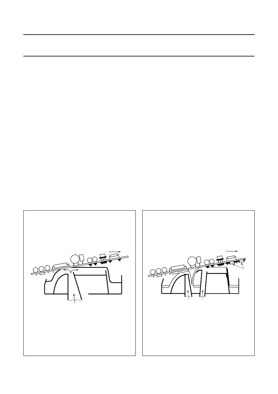
Wave soldering is usually the best method to use when
high throughput rates are required. The single-wave
soldering principle (see Fig.12) is the most straight forward
method and can be used on simple substrates with
two-terminal SMD components. More complex substrates
with increased circuit density and closer spacing of
conductors can pose the problems of nonwetting (dry
joints) and solder bridging. Bridging can occur across the
closely spaced leads of multi-leaded devices as well as
across adjacent leads on neighbouring components.
Nonwetting is usually caused by components with plastic
bodies. The plastic is not wetted by solder and creates a
depression in the solder wave, which is augmented by
surface tension. This can cause a shadow behind the
component and prevent solder from reaching the joint
surfaces. A smooth laminar solder wave is required to
avoid bridging and a high pressure wave is needed to
completely cover the areas that are difficult to wet. These
conflicting demands are difficult to attain in a single wave
but dual wave techniques go a long way in overcoming the
problem.
In a dual wave machine (see Fig.13), the substrate first
comes into contact with a turbulent wave which has a high
vertical velocity. This ensures good solder contact with
both edges of the components and prevents joints from
being missed. The second smooth laminar wave
completes the formation of the solder fillet, removes
excess solder and prevents bridging. Figure 14 indicates
the time/temperature relationship measured at the
soldering site in dual wave soldering.
New methods of wave soldering are developing
continually. For example, the Omega System is a single
wave agitated by pulses, which combines the functions of
smoothness and turbulence. In another, a lambda wave
injects air bubbles in the final part of the wave. A further
innovation is the hollow jet wave in which the solder wave
flows in the opposite direction to the substrate.
Fig.12 Single wave soldering principle.
board travel
MBC935
solder
Fig.13 Dual wave soldering principle.
handbook, halfpage
board travel
MBC934
solder
SMDs
1997 Nov 26
20
Philips Semiconductors
Product specification
Small-signal Field-effect Transistors
General section
Fig.14 Typical time-temperature curve measured
at the soldering site.
handbook, halfpage
0
300
200
100
0
50
100
150
MBC936
time (s)
T
o
( C)
250
150
50
200 K/s
1 K/s
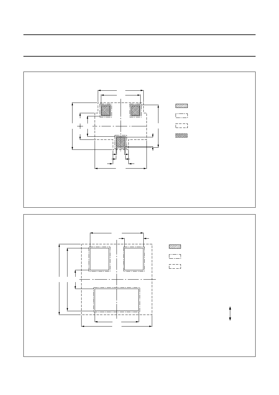
Footprint design
The footprint design of a component for surface mounting
is influenced by many factors:
•
features of the component, its dimensions and
tolerances
•
circuit board manufacturing processes
•
desired component density
•
minimum spacing between components
•
circuit tracks under the component
•
component orientation (if wave soldering)
•
positional accuracy of solder resist to solder lands
•
positional accuracy of solder paste to solder lands
(if reflow soldering)
•
component placement accuracy
•
soldering process parameters
•
solder joint reliability parameters.
1997 Nov 26
21
Philips Semiconductors
Product specification
Small-signal Field-effect Transistors
General section
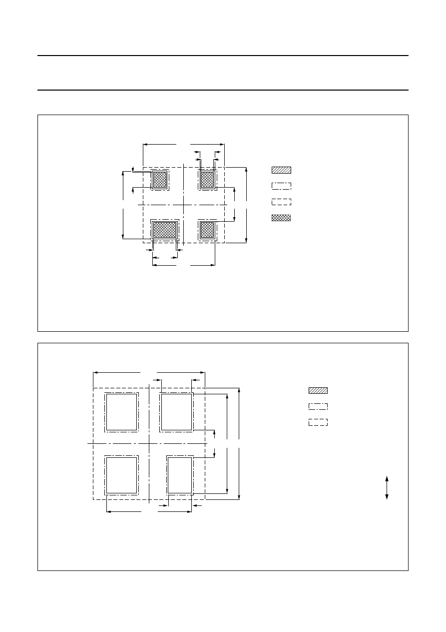
SOT23
FOOTPRINTS
Fig.15 Reflow soldering footprint for SOT23; typical dimensions.
Dimensions in mm.
Placement accuracy:
±
0.25 mm.
handbook, full pagewidth
,
,
MSA439
1.00
0.60
(3x)
1.30
1
2
3
2.50
3.00
0.85
2.70
,,
,,
,,
,,
2.90
0.50 (3x)
0.60 (3x)
3.30
0.85
solder lands
solder resist
occupied area
solder paste
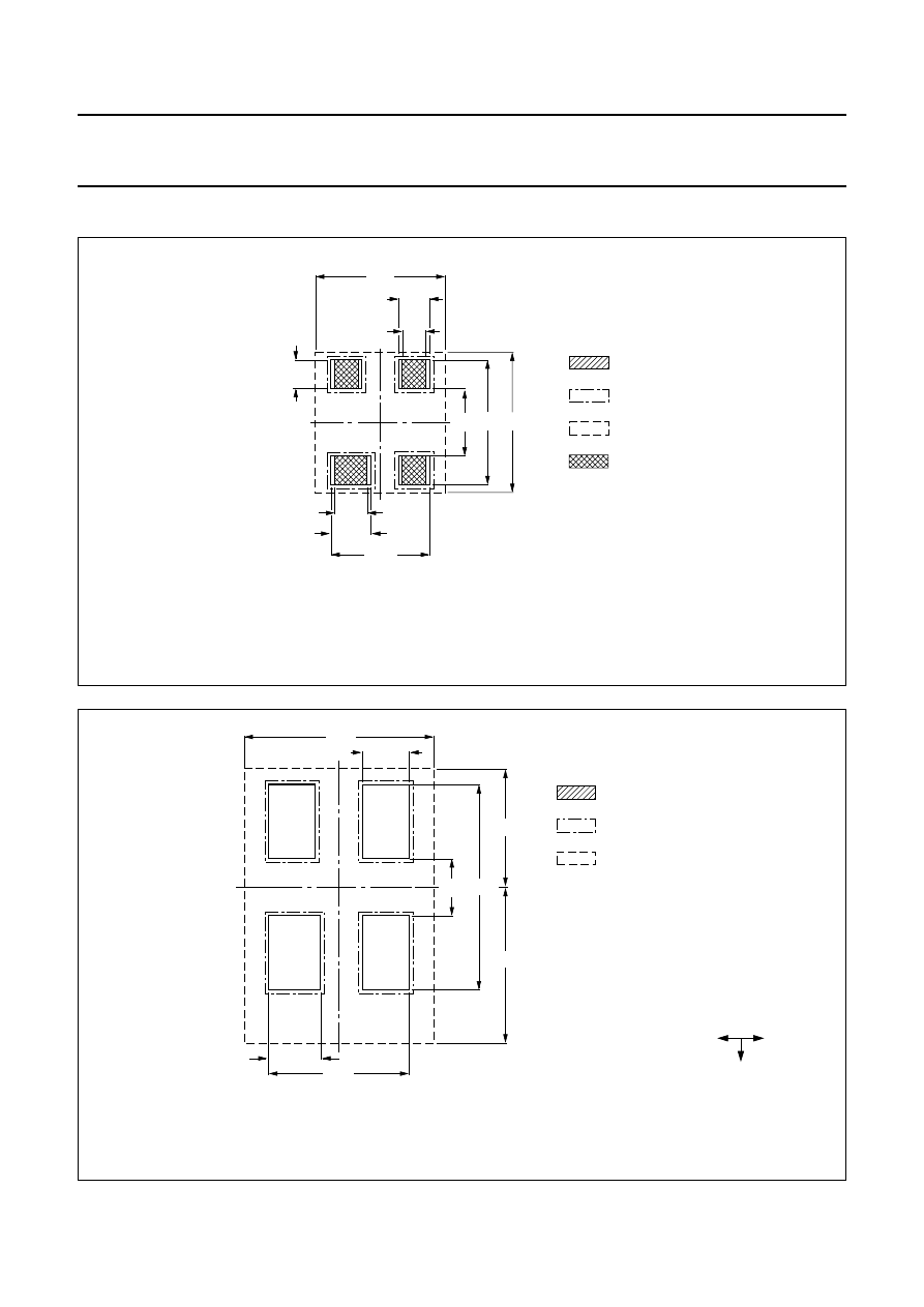
Fig.16 Wave soldering footprint for SOT23; typical dimensions.
Dimensions in mm.
Placement accuracy:
±
0.25 mm.
handbook, full pagewidth
MSA427
4.00
4.60
2.80
4.50
1.20
,,,,
,,,,
,,,,
,,,
,,,
,,,
,,,
,,,
,,,
3.40
3
2
1
1.20 (2x)
preferred transport direction during soldering
solder lands
solder resist
occupied area
1997 Nov 26
22
Philips Semiconductors
Product specification
Small-signal Field-effect Transistors
General section
SOT143/SOT143R
FOOTPRINTS
Fig.17 Reflow soldering footprint for SOT143; typical dimensions.
Dimensions in mm.
Placement accuracy:
±
0.25 mm.
handbook, full pagewidth
,,
,,
MSA441
0.60
(4x)
1.30
2.50
3.00
2.70
0.50 (3x)
0.60 (3x)
3.25
4
3
2
1
,,
,,
,,
,,
,,
,,
0.90
1.00
solder lands
solder resist
occupied area
solder paste
Fig.18 Wave soldering footprint for SOT143; typical dimensions.
Dimensions in mm.
Placement accuracy:
±
0.25 mm.
handbook, full pagewidth
MSA422
4.00 4.60
1.20 (3x)
4.45
1
2
3
4
1.15
,,
,,
,,
3.40
1.00
preferred transport direction during soldering
,,
,,
,,
,,
,,
,,
,,
,,
,,
solder lands
solder resist
occupied area
1997 Nov 26
23
Philips Semiconductors
Product specification
Small-signal Field-effect Transistors
General section
SOT343
FOOTPRINTS
Fig.19 Reflow soldering footprint for SOT343; typical dimensions.
Dimensions in mm.
Placement accuracy:
±
0.25 mm.
handbook, full pagewidth
MSA430
2.50
3
4
2
1
0.55
(4x)
2.40
,,
,,
,,
1.30
0.50
(3x)
1.90
,,
,,
,,
2.70
0.70
0.80
0.60
(3x)
solder lands
solder resist
occupied area
solder paste
Fig.20 Wave soldering footprint for SOT343; typical dimensions.
Dimensions in mm.
Placement accuracy:
±
0.25 mm.
handbook, full pagewidth
MSA421
4.00
3.00
2.30
0.90 (3x)
3.65
1
2
4
3
1.15
,,
,,
,,
2.70
1.00
transport direction during soldering
,,
,,
,,
,,
,,
,,
,,
,,
,,
solder lands
solder resist
occupied area

1997 Nov 26
24
Philips Semiconductors
Product specification
Small-signal Field-effect Transistors
General section
Hand soldering microminiature components
It is possible to solder microminiature components with a
light-weight hand-held soldering iron, but this method has
obvious drawbacks and should be restricted to laboratory
use and/or incidental repairs on production circuits:
•
hand-soldering is time-consuming and therefore
expensive.
•
the component cannot be positioned accurately and the
connecting tags may come into contact with the
substrate and damage it.
•
there is a risk of breaking the substrate and internal
connections in the component could be damaged.
•
the component package could be damaged by the iron.
THERMAL CONSIDERATIONS
Thermal resistance
Circuit performance and long-term reliability are affected
by the temperature of the transistor die. Normally, both are
improved by keeping the die temperature (junction
temperature) low.
Electrical power dissipated in any semiconductor device is
a source of heat. This increases the temperature of the die
about some reference point, normally an ambient
temperature of 25
o
C in still air. The size of the increase in
temperature depends on the amount of power dissipated
in the circuit and the net thermal resistance between the
heat source and the reference point.
Devices lose most of their heat by conduction when
mounted on a a printed board, a substrate or heatsink.
Referring to Fig.21 (for surface mounted devices mounted
on a substrate), heat conducts from its source (the
junction) via the package leads and soldered connections
to the substrate. Some heat radiates from the package into
the surrounding air where it is dispersed by convection or
by forced cooling air. Heat that radiates from the substrate
is dispersed in the same way.
The elements of thermal resistance shown in Fig.22 are
defined as follows:
R
th j-mb
thermal resistance from junction to mounting
base
R
th j-c
thermal resistance from junction to case
R
th j-s
thermal resistance from junction to soldering
point
R
th s-a
thermal resistance from soldering point to
ambient
R
th c-a
thermal resistance from case to ambient (R
th s-a
and R
th c-a
are the same for most packages)
R
th j-a
thermal resistance from junction to ambient.
The temperature at the junction depends on the ability of
the package and its mounting to transfer heat from the
junction region to the ambient environment. The basic
relationship between junction temperature and power
dissipation is:
T
j max
= T
amb
+ P
tot max
(R
th j-s
+ R
th s-a
)
= T
amb
+ P
tot max
(R
th j-a
)
where:
T
j max
is the maximum junction temperature
T
amb
is the ambient temperature
P
tot max
is the maximum power handling capability of the
device, including the effects of external loads
when applicable.
In the expression for T
j max
, only T
amb
and R
th s-a
can be
varied by the user. The package mounting technique and
the flow of cooling air are factors that affect R
th s-a
. The
device power dissipation can be controlled to a limited
extent but under recommended usage, the supply voltage
and circuit loading dictate a fixed power maximum. The
R
th j-s
value is essentially independent of external
mounting method and cooling air; but is sensitive to the
materials used in the package construction, the die
bonding method and the die area, all of which are fixed.
1997 Nov 26
25
Philips Semiconductors
Product specification
Small-signal Field-effect Transistors
General section
Values of T
j max
and R
th j-s
, or R
th j-c
or R
th j-a
are given in
the device data sheets. For applications where the
temperature of the case is stabilized by a large or
temperature-controlled heatsink, the junction temperature
can be calculated from
T
j
= T
case
+ P
tot
×
R
th j-c
or, using the soldering point
definition, from T
j
= T
solder
+ P
tot
×
R
th j-s
.
Thermal resistance (R
th s-a
and R
th c-a
)
The thermal resistance from soldering point to ambient
(SMDs), and that from case to ambient depends on the
mounting technique, the shape and material of the tracks
and substrate. Standard mounting conditions to set the
maximum power ratings of the various packages are
shown in Figs 23 to 37?. Each figure shows single-sided
35
µ
m copper-clad epoxy fibre-glass print, 1.5 mm thick,
the tracks are fully solder-tinned and the shaded areas
shown are copper or ceramic (Al
2
O
3
) 0.7 mm thick.
R
th s-a
for SMDs mounted on ceramic substrate
The thermal resistance R
th s-a
for devices in SOT23, 89,
143 and 223 packages mounted on ceramic substrate is a
function of the substrate area as shown in Fig.28.
The thermal resistance R
th j-a
can then be calculated by:
R
th j-a
(substrate) = R
th j-a
(PCB)
−
R
th s-a
(PCB)
+ R
th s-a
(substrate)
The R
th s-a
(PCB) is:
SOT23 and
SOT143
150 K/W
SOT89
140 K/W
SOT223
a function of pad area as shown in Fig.27.
Heat radiates from the package ‘1’ to ambient.
Heat conducts via leads ‘2’, solder joints ‘3’ to the substrate ‘4’.
Fig.21 Heat losses.
handbook, halfpage
,
,
,
MBB438
,
,
,,
,,
1
2
3
2
3
4
Fig.22 Representation of thermal resistance paths
of a device mounted on a substrate or
printed board.
handbook, halfpage
MBB439
R th j–s
ambient
junction
soldering
point or
case
R th j–a
R th c–a
R th j–mb R th j–c
=
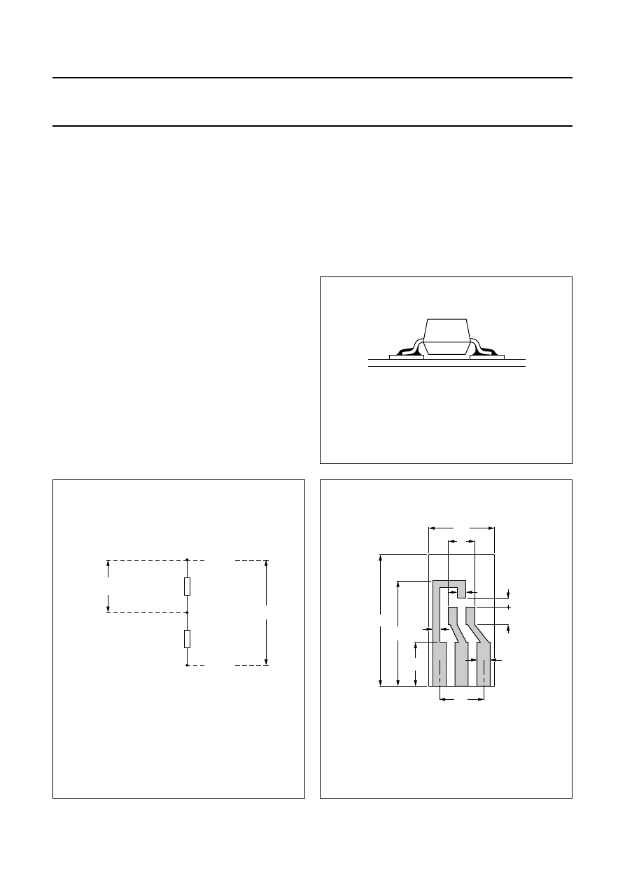
Fig.23 Standard mounting conditions for SOT23.
Dimensions in mm.
handbook, halfpage
MBB444
5.1
1.5
1
2
7.5
0.8
5
12
15
3
1
1997 Nov 26
26
Philips Semiconductors
Product specification
Small-signal Field-effect Transistors
General section
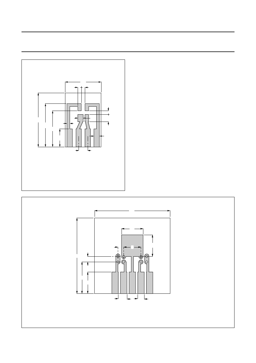
Fig.24 Standard mounting conditions for SOT143.
Dimensions in mm.
handbook, halfpage
MBB443
2.5
1.5
1
2
1.5
10
1
1
0.8
5
10
12
15
Fig.25 Standard mounting conditions for SOT54, higher dissipation option.
Dimensions in mm.
handbook, full pagewidth
MBE241
10
18
2.54
2.54
35
10
10
3
4
35
8
1997 Nov 26
27
Philips Semiconductors
Product specification
Small-signal Field-effect Transistors
General section
Fig.26 Standard mounting conditions for SOT54.
Dimensions in mm.
handbook, full pagewidth
MBE242
10
18
2.54
2.54
35
3
4
35
8
Fig.27 Thermal resistance (R
th j-a
) as a function of
FR4 epoxy fibre-glass circuit board.
handbook, halfpage
0
150
100
50
0
2
4
6
MGC124
R th j-a
Fcu(cm )
2
(K/W)
Fig.28 Thermal resistance (R
th s-a
) as a function of
area of ceramic substrate.
handbook, halfpage
10
MBB447
1
10
10
3
10
2
10
−
1
area (cm )
2
Rth s-a
(K/W)

1997 Nov 26
28
Philips Semiconductors
Product specification
Small-signal Field-effect Transistors
General section
ELECTROSTATIC CHARGES
Electrostatic charges can exist in many things; for
example, man-made-fibre clothing, moving machinery,
objects with air blowing across them, plastic storage bins,
sheets of paper stored in plastic envelopes, paper from
electrostatic copying machines, and people. The charges
are caused by friction between two surfaces, at least one
of which is non-conductive. The magnitude and polarity of
the charges depend on the different affinities for electrons
of the two materials rubbing together, the friction force and
the humidity of the surrounding air.
Electrostatic discharge is the transfer of an electrostatic
charge between bodies at different potentials and occurs
with direct contact or when induced by an electrostatic
field. Our devices can be damaged if the following
precautions are not taken.
WORK STATION
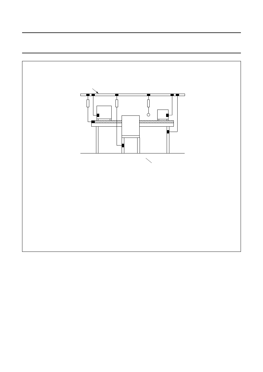
Figure 29 shows a working area suitable for safely
handling electrostatic sensitive devices. It has a work
bench, the surface of which is conductive or covered by an
antistatic sheet. Typical resistivity for the bench surface is
between 1 and 500 k
Ω
per cm
2
. The floor should also be
covered with antistatic material.
The following precautions should be observed:
•
Persons at a work bench should be earthed via a wrist
strap and a resistor.
•
All mains-powered electrical equipment should be
connected via an earth leakage switch.
•
Equipment cases should be earthed.
•
Relative humidity should be maintained between 50 and
65%.
•
An ionizer should be used to neutralize objects with
immobile static charges.
RECEIPT AND STORAGE
Our devices are packed for dispatch in
antistatic/conductive containers, usually boxes, tubes or
blister tape. The fact that the contents are sensitive to
electrostatic discharge is shown by warning labels on both
primary and secondary packing.
The devices should be kept in their original packing whilst
in storage. If a bulk container is partially unpacked, the
unpacking should be performed at a protected work
station. Any devices that are stored temporarily should be
packed in conductive or antistatic packing or carriers.
ASSEMBLY
The devices must be removed from their protective
packing with earthed component pincers or short-circuit
clips. Short-circuit clips must remain in place during
mounting, soldering and cleansing/drying processes. Do
not remove more devices from the storage packing than
are needed at any one time. Production/assembly
documents should state that the product contains
electrostatic sensitive devices and that special precautions
need to be taken.
All tools used during assembly, including soldering tools
and solder baths, must be earthed. All hand tools should
be of conductive or antistatic material and, where possible,
should not be insulated.
Measuring and testing of completed circuit boards must be
done at a protected work station. Place the soldered side
of the circuit board on conductive or antistatic foam and
remove the short-circuit clips. Remove the circuit board
from the foam, holding the board only at the edges. Make
sure the circuit board does not touch the conductive
surface of the work bench. After testing, replace the circuit
board on the conductive foam to await packing.
Assembled circuit boards should be handled in the same
way as unmounted devices. They should also carry
warning labels and be packed in conductive or antistatic
packing.
1997 Nov 26
29
Philips Semiconductors
Product specification
Small-signal Field-effect Transistors
General section
,,,,,,,,,,
handbook, full pagewidth
(1)
(2)
(3)
(4)
(2)
(6)
(2)
(7)
(8)
MLB049
(5)
(9)
Fig.29 Protected work station.
(1) Earthing rail.
(2) Resistor (500 k
Ω ±
10%, 0.5 W).
(3) Ionizer.
(4) Work bench.
(5) Chair.
(6) Wrist strap.
(7) Electrical equipment.
(8) Conductive surface/antistatic sheet.
(9) Antistatic floor.
Wyszukiwarka
Podobne podstrony:
SC07 98 IDEAS 1
SC07 98 REPLACEMENT 1
SC07 MARKING 98 1
SC17 GENERAL ROT 98 1
SC17 GENERAL MAG 98 1
(Art 98 a 100)
15 Sieć Następnej Generacjiid 16074 ppt
Solid Edge Generator kół zębatych
37 Generatory Energii Płynu ppt
98 37 WE id 48795 Nieznany (2)
40 0610 013 05 01 7 General arrangement
Eksploatowanie częstościomierzy, generatorów pomiarowych, mostków i mierników RLC
Biomass Fired Superheater for more Efficient Electr Generation From WasteIncinerationPlants025bm 422
Instrukcja generator sinusoidalny
97 98
98
F2A GENERALMATIC
General Electric
Opara S, Filozofia Współczesne kierunki i problemy, s 98 111
więcej podobnych podstron