Fusing Current
When Traces Melt Without a Trace
Douglas Brooks
This article appeared in Printed Circuit Design, a Miller Freeman publication, December, 1998
1998 Miller Freeman, Inc.
1998 UltraCAD Design, Inc.
Many people have contacted me regarding my column
“Trace Currents and Temperatures: How Hard Can We
Drive ‘Em?” in the May, 1998, issue. In that column I talked
about the possibilities and the problems associated with
developing a set of equations for the current/temperature
curves we all have occasion to reference.
But many of you posed a different question. It typically
went something like this: “I need the trace to carry 5 Amps
for only about .5 seconds before…“ something catastrophic
happens. “Then I don’t care if the trace melts or not. What
size trace do I need?”
My first reaction was that this is a fuse question, some-
thing I’ve never seen discussed. When enough of you asked
me about it I began digging for information. What I found
was there isn’t much to be found! But thanks to some
direction from a few experts in the field (Note 1) I discovered
that there is some very interesting theory to draw from.
CAUTION: The information that follows is based on
theory and, to my knowledge, has never been tested on
printed circuit boards. Designs based on this theoretical
discussion should be significantly derated and/or tested be-
fore being committed to production.
Preece’s Investigation:
W. H. Preece investigated the fusing (melting) current of
a wire. He developed Equation 1 for fusing current (Note 2):
I = a*d
3/2
Eq. 1
where I is the fusing current, d is the diameter of the
wire in inches, and a is a constant that depends on the
material. He determined that a = 10,244 for copper.
A little algebra transforms this equation to:
I = 12,277*A
.75
Eq. 2
where I = fusing current in Amps and A = the cross
sectional area of the wire in square inches.
Validation:
In my previous article I started with the relationship
I = k*DT
B1
*A
B2
where I = Current in Amps, DT = change in temperature
in
o
C., and A = cross sectional area in square mils.
Although I demonstrated that results could be improved
if Area were broken into its component parts of width and
thickness, the data still fit this model well and produced an
empirical “best fit” equation:
I = .04*DT
.45
A
.69
Now the melting point of copper is about 1083
o
C, result-
ing in a DT from room temperature of about 1063
o
C.
Plugging this value for DT into the equation and converting A
to square inches leads to
I = 12,706*A
.69
Eq. 3
These two results (Equations 2 and 3) are remarkably
close considering how different is their source and approach!
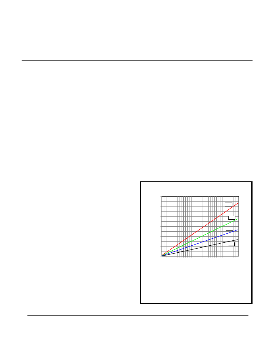
Onderdonk’s Investigation:
I. M. Onderdonk developed a fairly complicated equation
that relates current and the time it takes for a wire to melt
(Note 3). Using the melting point of copper for Tm and
converting area to square mils, his equation reduces to:
I = .188*A/t
.5
Eq. 4
In this equation, I is the amount of current (Amps) that
can be applied to a trace of cross sectional area A square mils
for t seconds before the trace melts. Figure 1 graphs this
relationship.
0
20
40
60
80
100
120
Current, Amps
50
100 150 200 250 300 350 400
Area, Sq. Mils
Fusing Current Vs Area
T=.5
T=1
T=2
T=5
Figure 1.
Relationship between fusing current, cross-
sectional area and time for PCB traces, based on
Onderdonl’s equation.
Example:
Assume a 1 oz. (1.35 mil thick) copper trace must carry
20 Amps for 5 seconds. How wide must it be? Equation 4
leads to 176 mils in width. (Remember, there is NO safety
margin in this calculation!)
Discussion:
Trace current/temperature studies we are familiar with
have tried to discover the equilibrium temperature a trace
will reach when a current is applied. Equilibrium occurs
when the heating of the trace (I
2
R) is the same as the
cooling of the trace through convection and conduction.
Preece’s equation reportedly assumes no heat loss except
through radiation; i.e. no heat is conducted away from the
wire. In practice on a PCB, there is heat conducted away
from the trace by the board material itself, and by pads and
components, etc. On the other hand, heat loss would be
minimal in most applications in the first few seconds,
especially in the first few fractions of a second. In this
regard, Preece’s assumption appears to be a good one for a
PCB application.
It is possible to calculate an “implied” time to failure
for Preece’s equation by setting it equal to Onderdonk’s and
solving for time. When this is done, the implied “time” for
Preece’s equation to reach the melting point is purely a
function of area and is given by:
T = .233*A
.5
where A is the cross sectional area of the trace in
square mils. Table 1 shows this relationship.
Summary:
Preece’s and Onderdonk’s equations seem to be
straightforward ways to calculate fusing time and current
for PCB traces when it is only necessary that the trace not
fail (melt) within a defined period of time (say 10 seconds
or less.) But they are not meant to be applied to longer
periods of time. And remember, they have not been verified
empirically on PCBs, so use them with caution and derate
them appropriately.
Area, Sq. Mils
Time, Secs
10
0.7
20
1.0
50
1.6
100
2.3
200
3.3
500
5.2
1000
7.4
Table 1
Implied fusing time for Preece's equation
based on Onderdonk's equation.
Notes:
1 I am indebted to Ralph Hersey, Ralph Hersey and Asso-
ciates, Livermore, CA., and then Rich Nute, Hewlett
Packard, San Diego, CA. for pointing me toward
Onderdonk’s and Preece’s equations.
2. See “Standard Handbook for Electrical Engineers,” 12
Ed., McGraw-Hill, p. 4-74
3. Ibid. Onderdonk’s equation is
I = A*(log(1 + (Tm-Ta)/(234+Ta))/33*s)
.5
Where I = current in Amps, A = cross sectional area
in circular mils, Tm = melting temperature of the
material in
o
C, Ta = ambient temperature, also in
o
C,
and s = time in seconds.
Wyszukiwarka
Podobne podstrony:
O’Hurley 04 Without A Trace
Roberts, Nora O Hurleys 4 Without a Trace
fusingsilver
Current Clinical Strategies, Psychiatry History Taking (2004) BM OCR 7 0 2 5
Power Source Current Flow Chart
Immunonutrition in clinical practice what is the current evidence
Current Clinical Strategies, Physicians' Drug Resource (2005) BM OCR 7 0 2 5
How and When to Be Your Own Doctor
Nyambe When Giraffes Attack
Constant current driving of the RGB LED
glossary current
Aleister Crowley Magick Without Tears
Marketing Without Advdertising eBook EEn
when september ends
Without you
M 5521 Dress without shoulder straps
jednostki weterynaryjne w systemie TRACES
Gigerentzer, Hertwig The Priority Heuristic Making Choices Without Trade Offs
Guide To Currency Trading Forex
więcej podobnych podstron